Pole Position SP-218 3rd Printing
Pole Position (World) (Namco, 1982) · Schematic Package · 32 pages · 73 sections · original scan
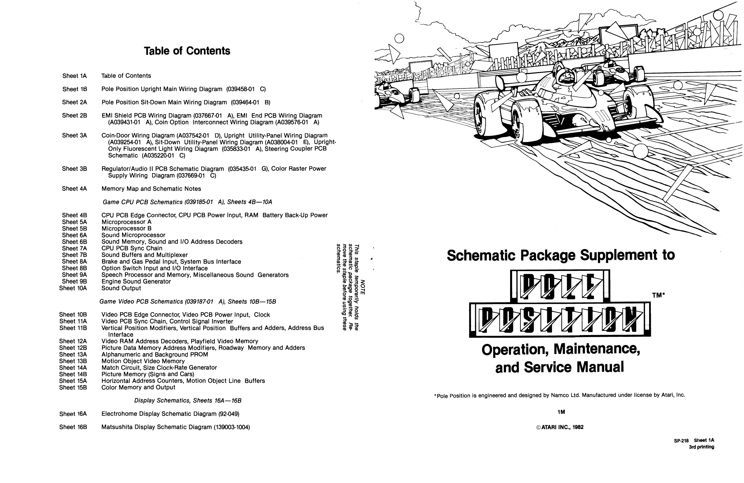
Sheet 1A
Sheet 1B
Sheet 2A
Sheet 2B
Sheet 3A
Sheet 3B
Sheet 4A
Sheet 4B Sheet 5A Sheet 5B Sheet 6A Sheet 6B Sheet 7A Sheet 7B Sheet 8A Sheet 8B Sheet 9A Sheet 9B Sheet 10A
Sheet 10B Sheet 11A Sheet 11B
Sheet 12A Sheet 12B Sheet 13A Sheet 13B Sheet 144 Sheet 14B Sheet 15A Sheet 15B
Sheet 16A
Sheet 16B Table of Contents
Table of Contents
Pole Position Upright Main Wiring Diagram (039458-01 C)
Pole Position Sit-Down Main Wiring Diagram (039464-01 B)
EMI Shield PCB Wiring Diagram (037667-01 A), EMI End PCB Wiring Diagram (A039431-01 A), Coin Option Interconnect Wiring Diagram (A039576-01 A)
Coin-Door Wiring Diagram (A037542-01 D), Upright Utility-Panel Wiring Diagram (A039254-01 A), Sit-Down Utility-Panel Wiring Diagram (A038004-01 &), Upright- Only Fluorescent Light Wiring Diagram (035833-01 A), Steering Coupler PCB Schematic (A035220-01 C)
Regulator/Audio Il PCB Schematic Diagram (035435-01 G), Color Raster Power Supply Wiring Diagram (037669-01 C)
Memory Map and Schematic Notes
Game CPU PCB Schematics (039185-01 A), Sheets 4B—10A
CPU PCB Edge Connector, CPU PCB Power Input, RAM Battery Back-Up Power Microprocessor A Microprocessor B Sound Microprocessor Sound Memory, Sound and I/O Address Decoders CPU PCB Sync Chain Sound Buffers and Multiplexer Brake and Gas Pedal Input, System Bus Interface Option Switch Input and I/O Interface Speech Processor and Memory, Miscellaneous Sound Generators Engine Sound Generator Sound Output
Game Video PCB Schematics (039187-01 A), Sheets 10B—15B
Video PCB Edge Connector, Video PCB Power Input, Clock Video PCB Sync Chain, Control Signal Inverter Vertical Position Modifiers, Vertical Position Buffers and Adders, Address Bus Interface Video RAM Address Decoders, Playfield Video Memory Picture Data Memory Address Modifiers, Roadway Memory and Adders Alphanumeric and Background PROM Motion Object Video Memory Match Circuit, Size Clock-Rate Generator Picture Memory (Signs and Cars) Horizontal Address Counters, Motion Object Line Buffers Color Memory and Output
Display Schematics, Sheets 16A—16B
Electrohome Display Schematic Diagram (92-049)
Matsushita Display Schematic Diagram (139003-1004) “soneweyos asay; Buysn asojaq ajdeys ay) anow ey 4843960} abeyoed onewayos ay} spjoy Ajjsesodwa} ajdeys siyt
ALON
Operation, Maintenance, and Service Manual
*Pole Position is engineered and designed by Namco Ltd. Manufactured under license by Atari, Inc.
1M
©ATARI INC., 1982
SP-218 Sheet 1A ‘3rd printing
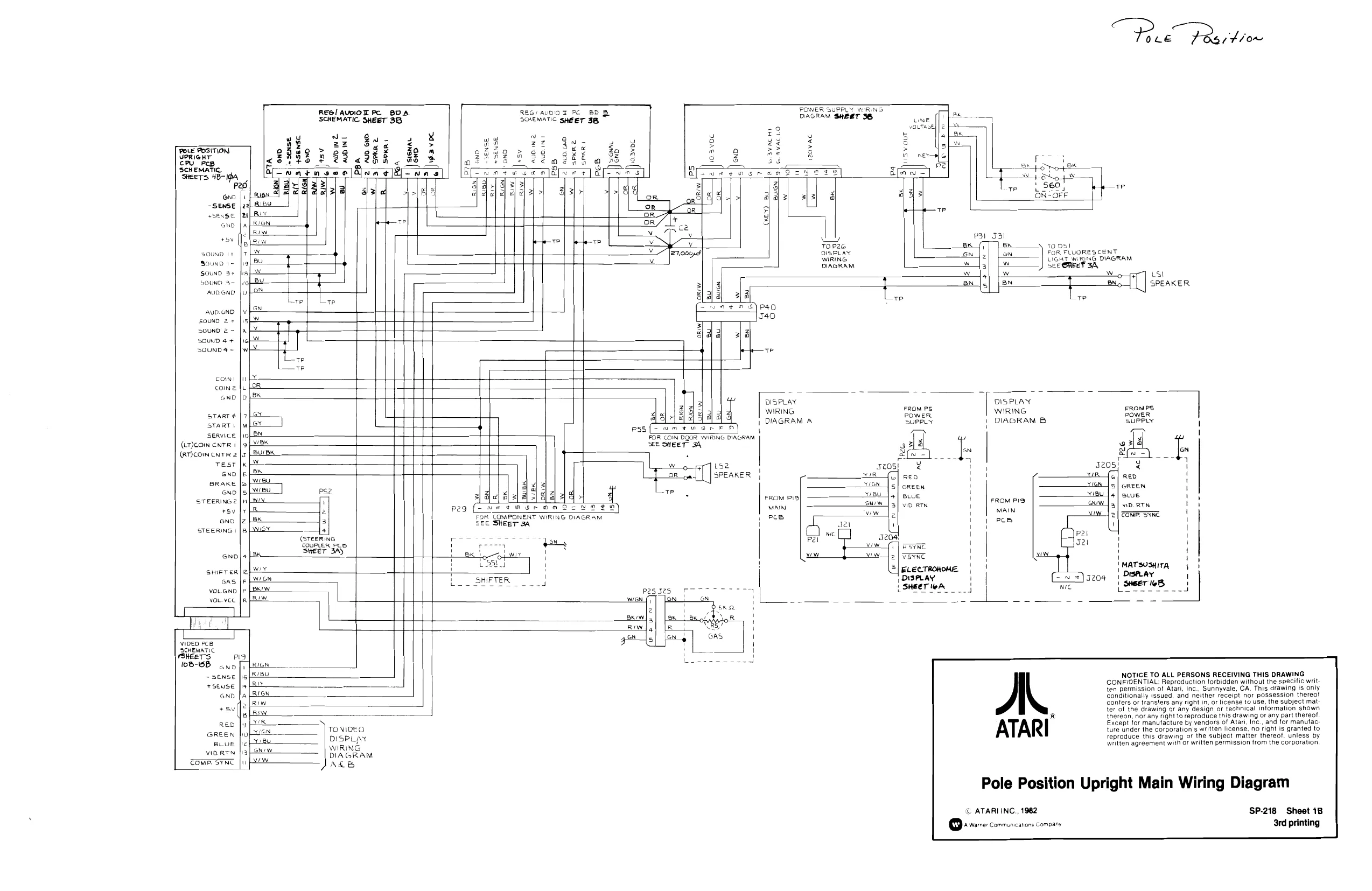
This page is a drawing, shown as the original scan.
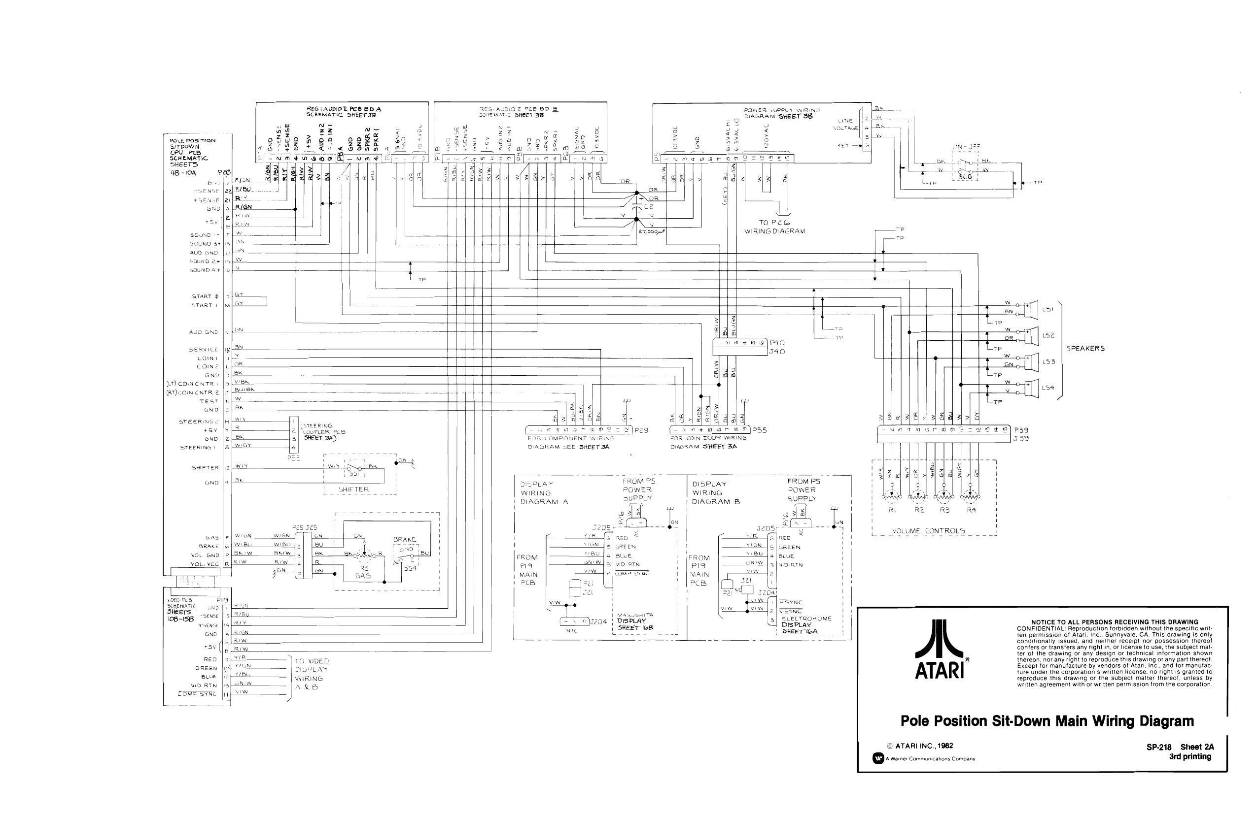
This page is a drawing, shown as the original scan.
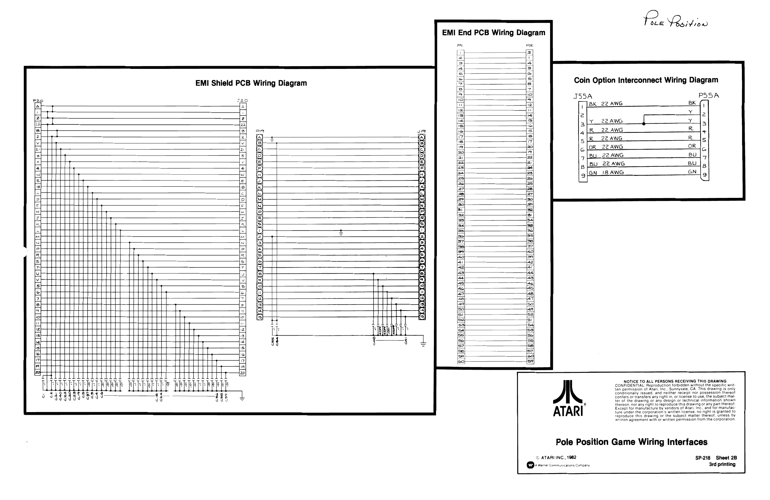
This page is a drawing, shown as the original scan.
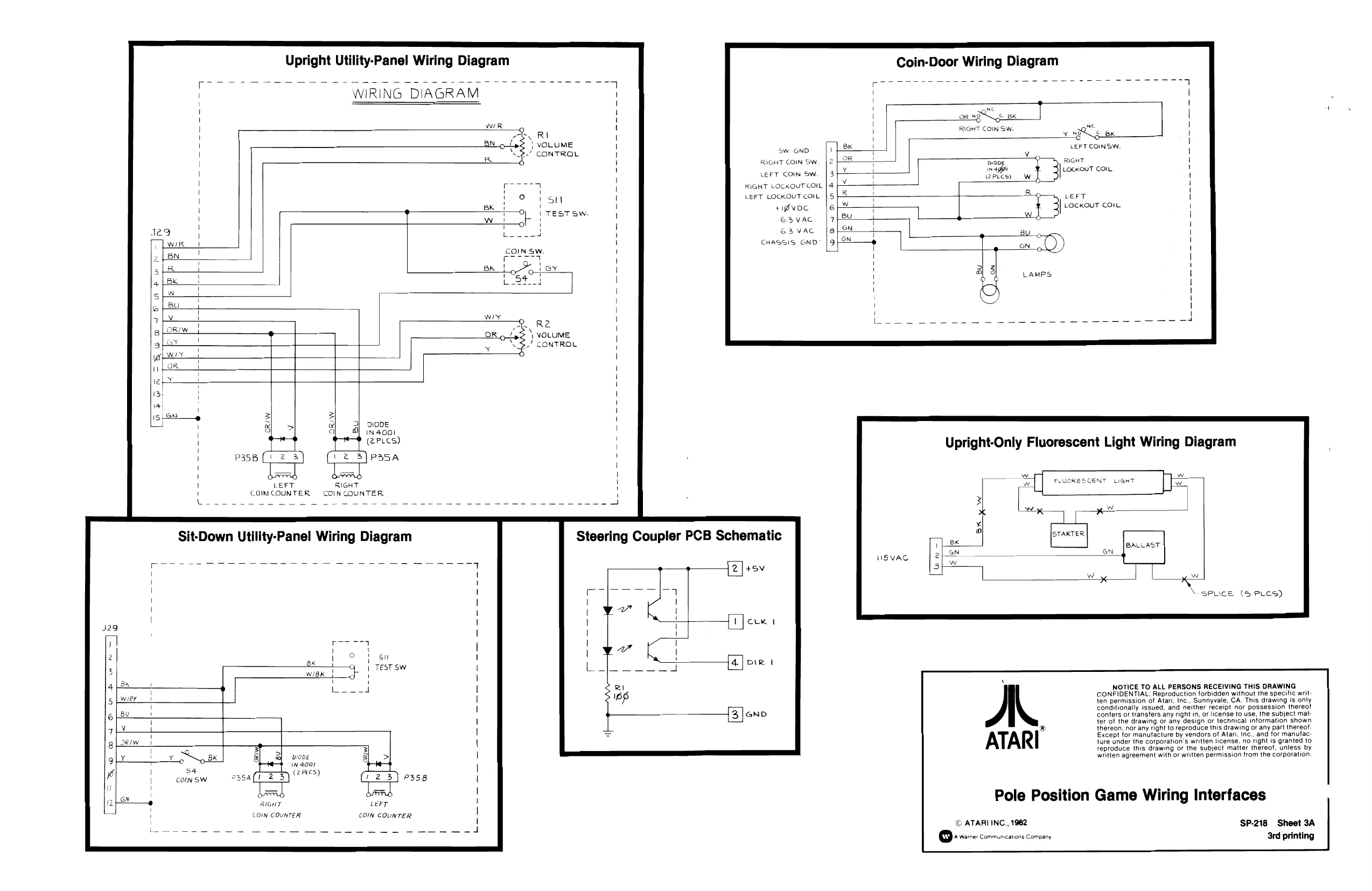
Upright Utility-Panel Wiring Diagram
WIRING DIAGRAM
ERI } VOLUME CONTROL
Re + OR 4/49 ) VOLUME, 3-1 CONTROL
DIODE q IN 4001 (2PLcs) p35B (1 2 3 23) P35a Bu
LEFT RIGHT COINCOUNTER COIN COUNTER,
Coin-Door Wiring Diagram
RIGHT COIN SW. + NIA ak
Sw. GND.
RIGHT COIN SW.
LEFT COIN SW.
RIGHT LOCKOUT COIL
LEFT LOCKOUT COIL +1GNDC
63 VAC
63 VAC
CHASSIS GND DIODE ror (pecs) WW.
R Seaearon-] wt “8 LEFT COINSW. RIGHT | LoceouT com,
Lert LOCKOUT COIL,
Upright-Only Fluorescent Light Wiring Diagram
RESCENT Light
STARTER
ia Sy Bk
COIN SW
RIGHT
COIN COUNTER LEFT
COIN COUNTER V5 VAC f
ATARI
© ATARI INC., 1982 0S PLER):
NOTICE TO ALL PERSONS RECEIVING THIS DRAWING CONFIDENTIAL: Reproduction forbidden without the specific writ: ten permission of Atari, Inc., Sunnyvale, CA. This drawing is only conditionally issued, and neither receipt nor possession thereot confers or transters any right in, or license to use, the subject mat. ter of the drawing or any design or technical information shown thereon, nor any right to reproduce this drawing or any part thereof. Except for manufacture by vendors of Atari, Inc.. and for manufac: ture under the corporation's written license. no right is granted to reproduce this drawing or the subject matter thereof. unless by written agreement with or written permission from the corporation.
Pole Position Game Wiring Interfaces
‘SP-218 Sheet 3A
3rd printing
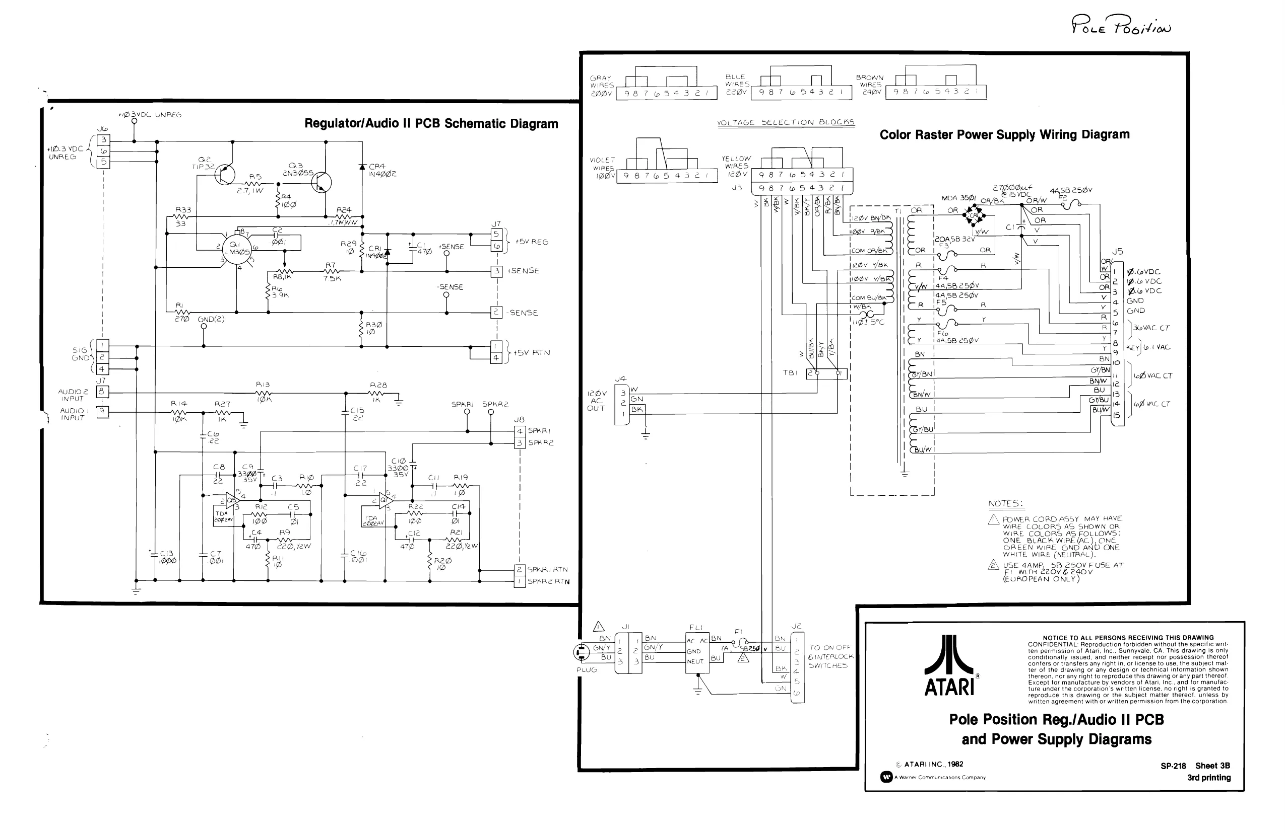
This page is a drawing, shown as the original scan.
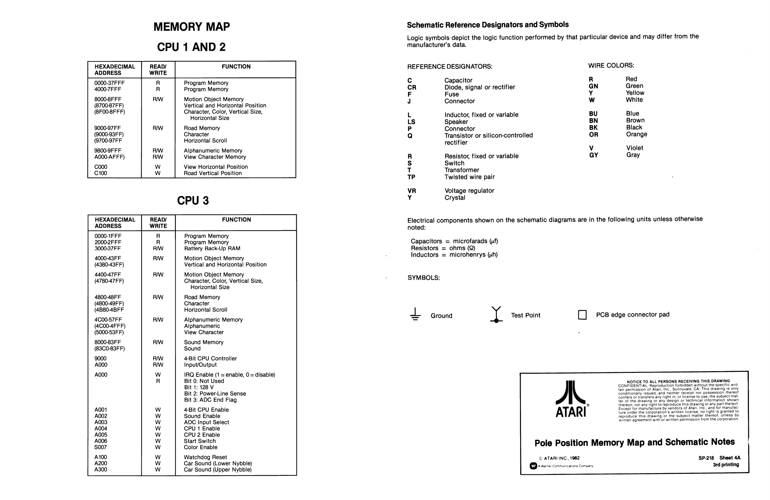
MEMORY MAP Schematic Reference Designators and Symbols
Logic symbols depict the logic function performed by that particular device and may differ from the CPU 1 AND 2 manufacturer's data.
HEXADECIMAL FUNCTION REFERENCE DESIGNATORS: WIRE COLORS: 0000-37FFF Program Memory Cc Capacitor R Red
ADDRESS
4000-7F FF Program Memory CR Diode, signal or rectifier GN Green
| F | Fuse | Y | Yellow |
| 8000-8F FF | Motion Object Memory | i |
e700 87FF) Vertical and Horizontal Position J Connector w White ‘ 9 Horizontal Size —— L Inductor, fixed or variable BU Blue (9700-97FF Horizontal Scroll Q ital or silicon-controlled OR Orang
FO0-8F F: Chi ter, Color, Vertical Size, .
| Ls | Speaker | BN | Brown | ||
| pei | Goad ial | Pp | Connector | BK | Black |
5 laracter + an 7 range
| 9800-9F FF | Alphanumeric Memory | Vv | Violet | ||
| A000-AFFF) | View Character Memory | R | Resistor, fixed or variable | GY | Gray |
000 View Horizontal Position s Switch
| C100 | Road Vertical Position | T | Transformer | | |
TP Twisted wire pair
Voltage regulator Crystal <<
HEXADECIMAL ADDRESS
0000-1FFF 2000-2FFF 3000-37FF 4000-43FF FUNCTION Electrical components shown on the schematic diagrams are in the following units unless otherwise noted: Program Memory Program Memory Battery Back-Up RAM Capacitors = microfarads (uf) Resistors = ohms (2) Inductors = microhenrys (uh) Motion Object Memory (4380-43FF) Vertical and Horizontal Position 4400-47FF Motion Object Memory
| (4780-47FF) | Character, Color, Vertical Size, | SYMBOLS: |
Horizontal Size 4800-48FF Road Memory (4800-49F F) Character
| (4B80-4BFF | Horizontal Scroll | tL | ||||
| 4C00-57FF | Alphanumeric Memory | Ground | a¢ | Test Point | oO | PCB edge connector pad |
(4C00-4FFF) Alphanumeric (6000-53FF) View Character 8000-83FF Sound Memory (83C0-83FF) Sound 9000 4-Bit CPU Controller A000 Input/Output A000 IRQ Enable (1 = enable, 0 = disable) Bit 0: Not Used Bit 1: 128 V Bit 2: Power-Line Sense Bit 3: ADC End Flag NOTICE TO ALL PERSONS RECEIVING THIS DRAWING CONFIDENTIAL: Reproduction forbidden without the specific writ ten permission of Atari, Inc., Sunnyvale, CA. This drawing is only Conditionally issued, and neither receipt nor possession thereof conters or transfers any right in, of license to use, the subject mat. ® ter of the drawing or any design or technical information shown thereon, nor any right to reproduce this drawing or any part thereof, 4-Bit CPU Enable ATARI Except for manuiacture by vendors of Ata Inc, and for manulac ture under the corporation's written license, no right is grante ADC Input Select written agreement with or written permission from the corporation. CPU 1 Enable CPU 2 Enable Start Switch Pole Po:
© ATARI INC., 1982 ‘SP-218 Sheet 4A + ve20: conmuncanons Company 3rd printing Color Enable n Memory Map and Schematic Notes
Watchdog Reset Car Sound (Lower Nybble) Car Sound (Upper Nybble) SSS SSSSSSE
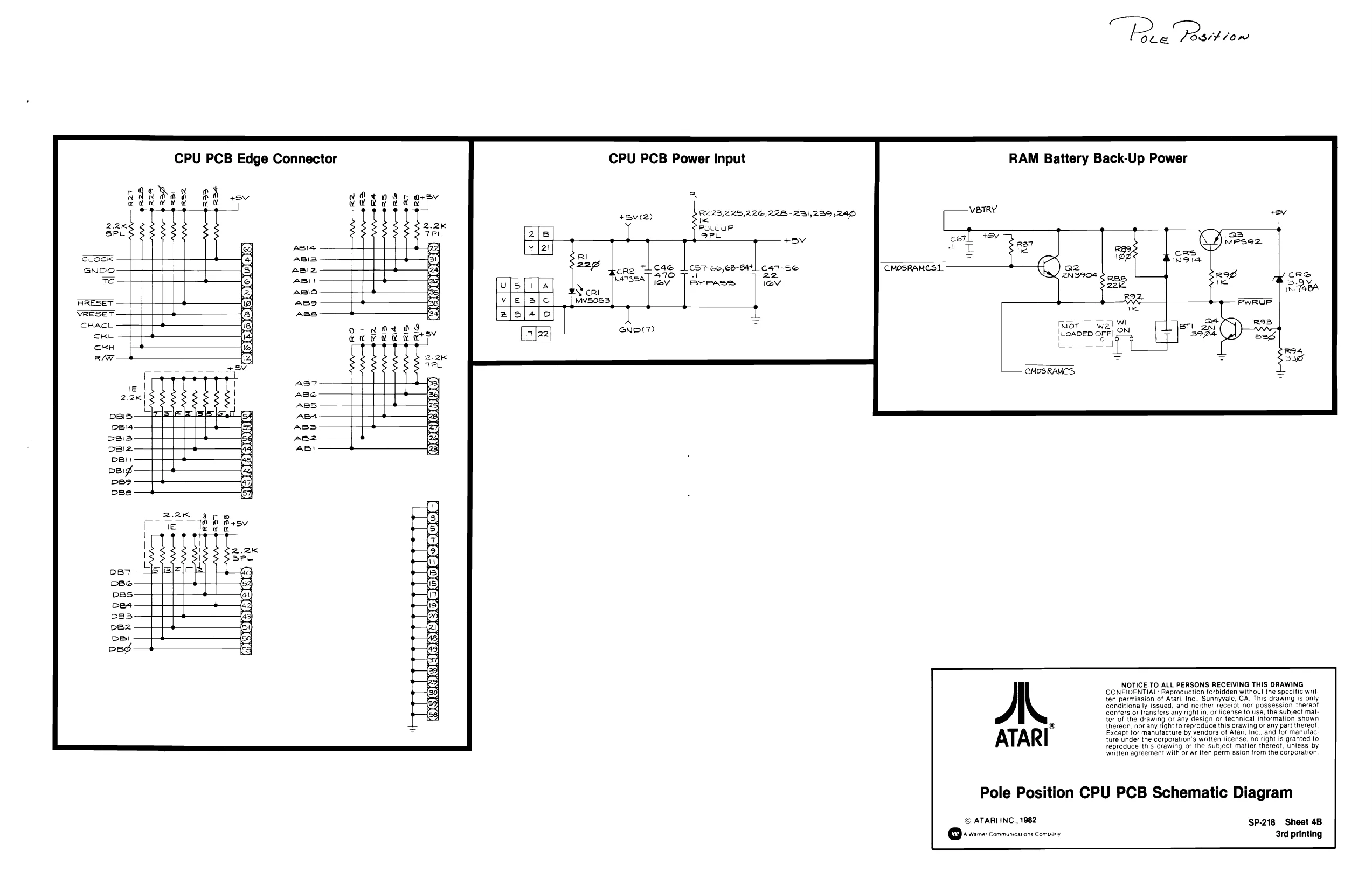
“Be 7 OStA On
RAM Battery Back-Up Power
CPU PCB Edge Connector CPU PCB Power Input
P BA wv R2 Re Re -——-VeTRY R2Z23,225,226,228-23),239,240 he PULLUP 2|8 aru +5v(2) +5V coal tev: aia we cRS BNol4
Ree 22K Roz.
Me oT wal Wh \Scaben OFFI bo ee od 57-60, 68-644] c47-5e 470 7 22 neennueel: tev | Brreass lov 2N3904 INQT354\
ziS|4/0 I @ND(7)
NOTICE TO ALL PERSONS RECEIVING THIS DRAWING CONFIDENTIAL: Reproduction forbidden without the specific writ ten permission of Atari, Inc., Sunnyvale, CA, This drawing is only Conditionally issued, and neither receipt nor possession thereo!
confers of transfers any right in, or license to use, the subject mat
ter of the drawing or any design or technical information shown
thereon, nor any right to reproduce this drawing or any part thereot
Except for manufacture by vendors of Atari, Inc,, and for manufac: ture under the corporation's written license. no right is granted to reproduce this drawing or the subject matter thereof, untess by written agreement with or written permission from the corporation
Pole Position CPU PCB Schematic Diagram
© ATARI INC., 1982 SP-218 Sheet 4B + Ware: Communcanors Company 3rd printing
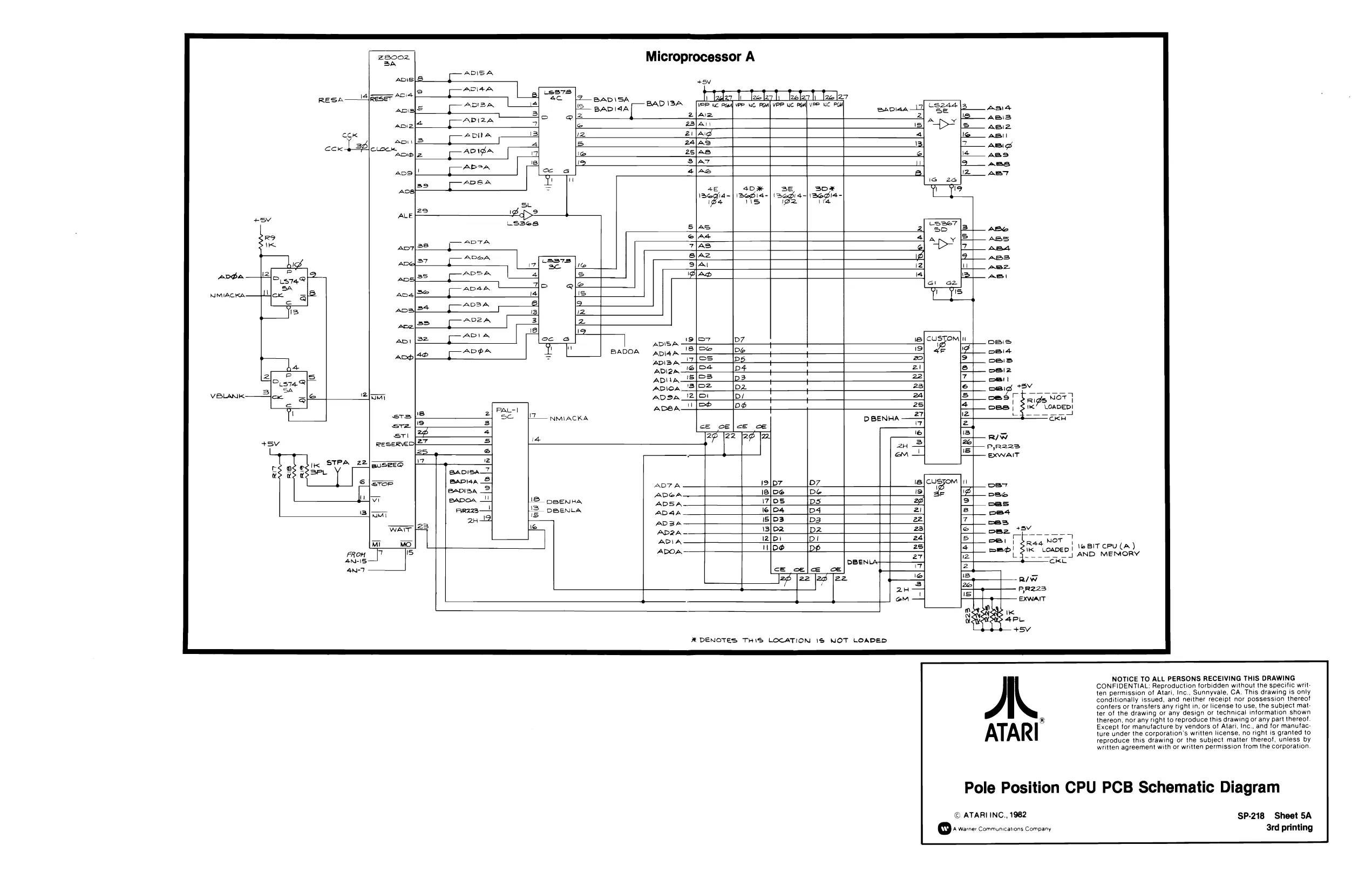
}2—BADISA H2— Bapiaa
Microprocessor A
+5
Part fi BAD ISA. We Ne Fa
lo
lx STPA 22 NMIACKA oss custom ae a cas
cai eel cag *SV
% w2Pk
© oBeNHA
DBENLA ‘5
Ie DBENHA Re FF] <P] R=
Rw PyRe2S mwa
CST pao pes ces ces +sv pee SY
DENOTES THIS LOCATION 1S NOT LOADED
ATARI
Canal 1K LOADED | 6-t >For 2E8 fT Saige NOT] pee 31? Loan! a
| We BIT CPU(A) | AND MEMORY
NOTICE TO ALL PERSONS RECEIVING THIS DRAWING CONFIDENTIAL; Reproduction forbidden without the specitic writ: ten permission of Atari, Inc., Sunnyvale, CA. This drawing is only conditionally issued, and neither receipt nor possession thereof
confers or transters any right in, or license to use, the subject mat
ter of the drawing or any design or technical information shown
thereon, nor any right to reproduce this drawing or any part thereot,
Except for manufacture by vendors of Atari, Inc., and for manufac. ture under the corporation's written license, no right is granted to reproduce this drawing or the subject matter thereof, unless by written agreement with or written permission from the corporation.
Pole Position CPU PCB Schematic Diagram
© ATARIINC., 1982 SP-218 Sheet 5A 3rd printing
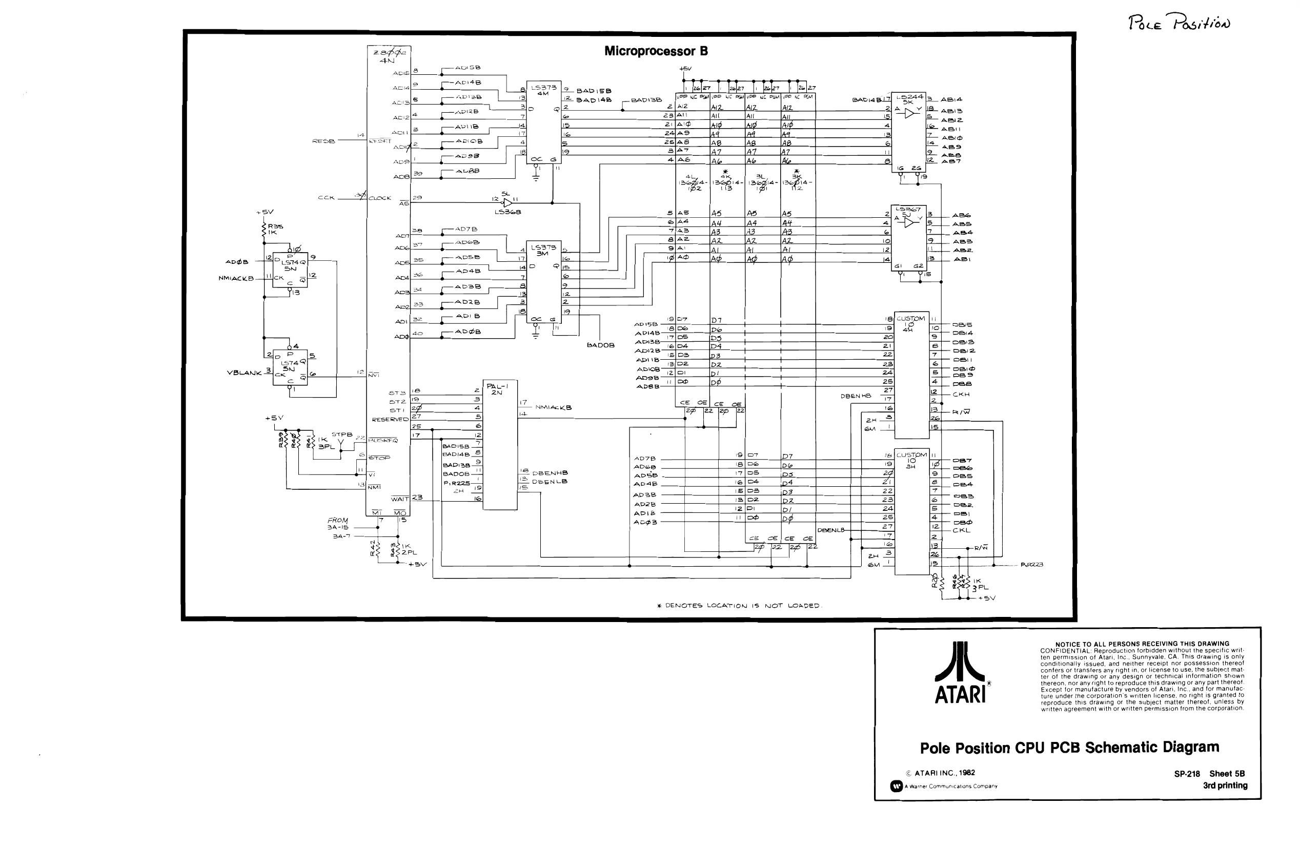
[eshge} AN ave[s SAPS s An4e Acid f S373, }2 Bapise
Microprocessor B
7 |) [aeler a ara Ree “Position
| 5 | Apres | 12 BaDiae | ou S244] | neia | ||
| ADI | 2] | " | Al | alan | y lie | ae: |
| soft | e | it —— | gps | |||
| son [2 | Pe | E | ie | __iay | 4 | be nei |
| A | Eve | 1; |
RESB ——J er St ADIOB Aad
| acg2 | [= | ; | aa | lap | P | ls nes |
; ares im ase
| a | bo | Ae | Iz ner |
" - \s_26 & Fe opis f
reac)
te[custom | 1S PRE BPP PPPS
- DENOTES LOCATION 1S NOT LOADED
NOTICE TO ALL PERSONS RECEIVING THIS DRAWING CONFIDENTIAL: Reproduction forbidden without the specific writ: ten permission of Atari, Inc., Sunnyvale, CA. This drawing is only conditionally issued, and neither receipt nor possession thereot Confers or transters any right in, or license to use, the subject mat ter of the drawing or any design or technical information shown
a thereon, nor any right to reproduce this drawing or any part thereot
Except for manufacture by vendors of Atari, Inc., and for manutac. ture under the corporation's written license, no right is granted to reproduce this drawing or the subject matter thereof. unless by written agreement with or written permission from the corporation.
Pole Position CPU PCB Schematic Diagram
© ATARI INC., 1982 SP-218 Sheet 5B + H2r06: Communicatons Company 3rd printing
This page is a drawing, shown as the original scan.
This page is a drawing, shown as the original scan.
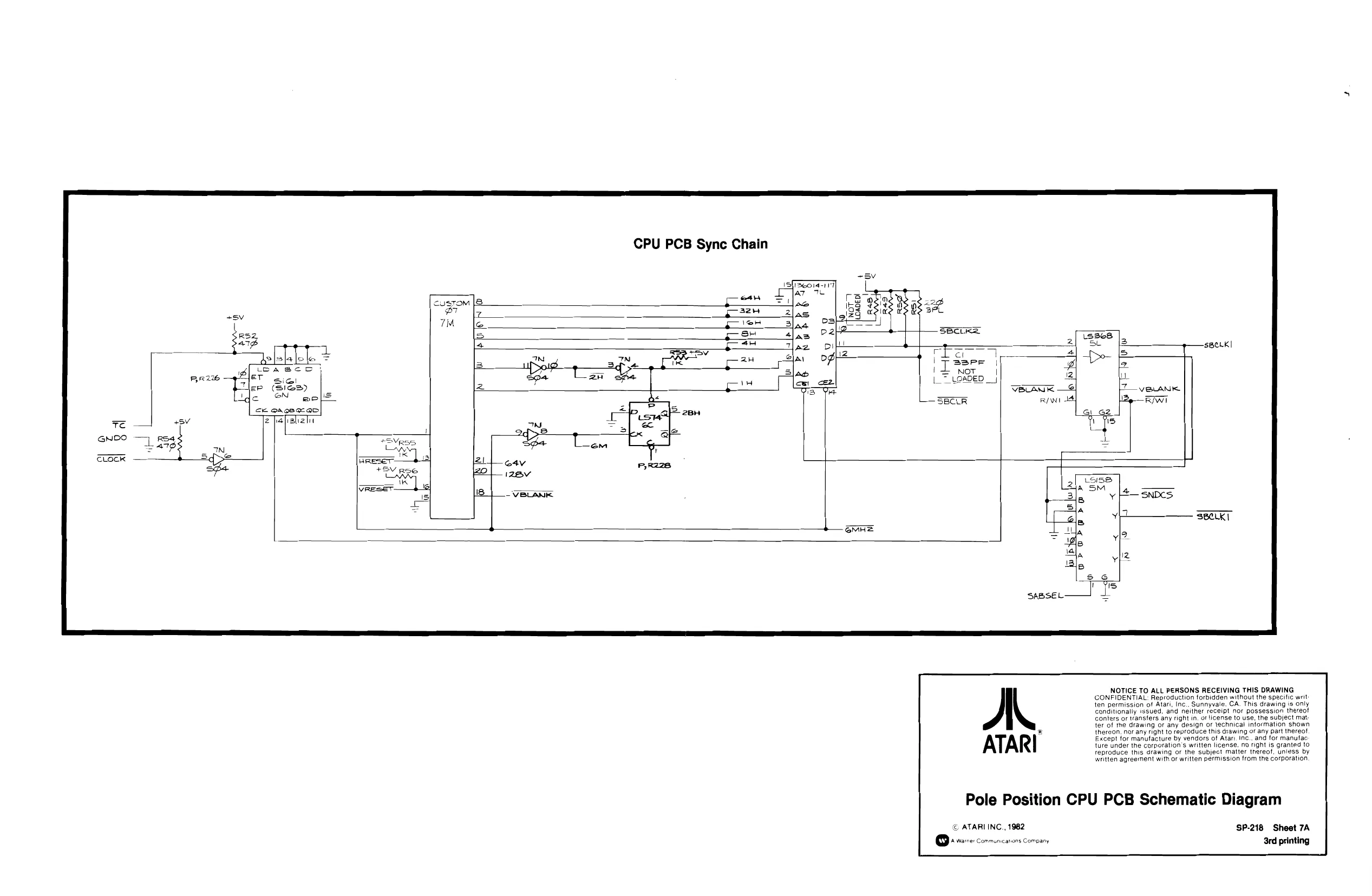
This page is a drawing, shown as the original scan.
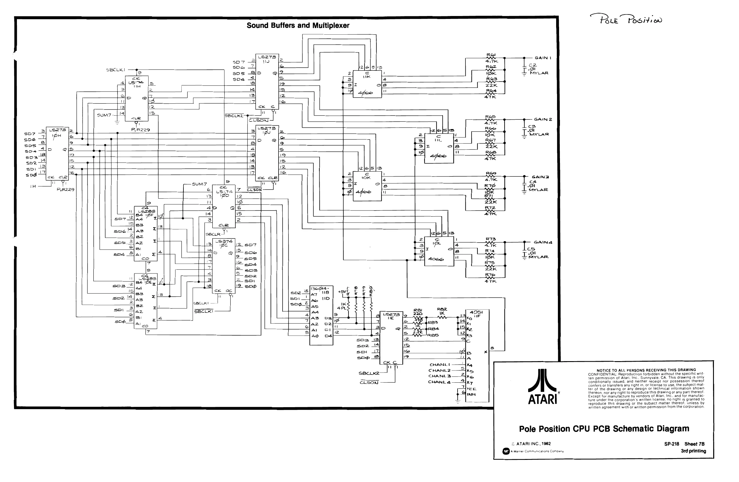
This page is a drawing, shown as the original scan.
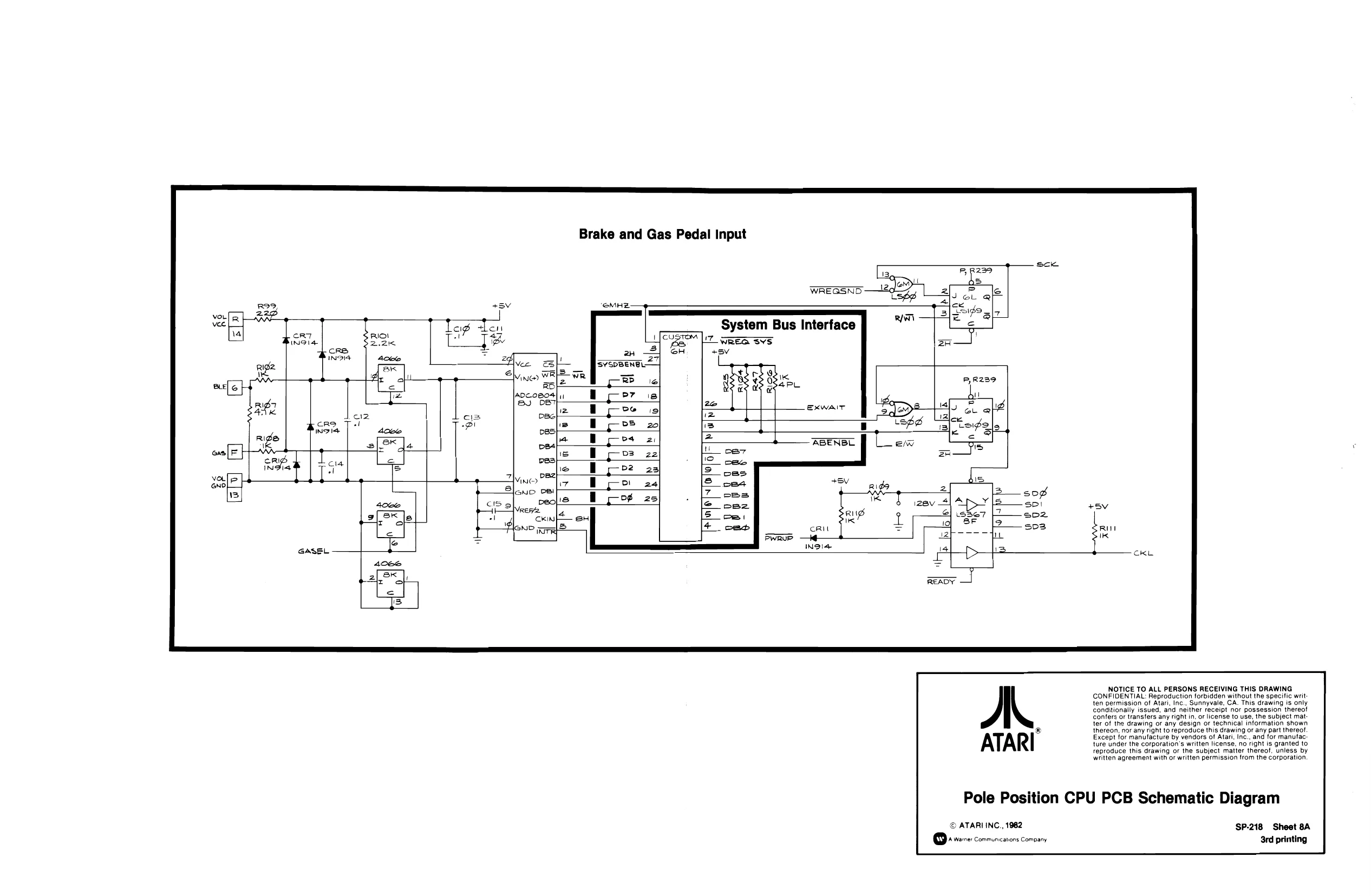
Brake and Gas Pedal Input
sv
log ston System Bus Interface
ew YE |? REG SVS cRe + +sv INDIA z Mec SS |SYSDBENBLing) WRI a iis) s— JADc. 0804 D7 BJ 08 =
De
oes
bes!
pes} ExXwait
confers or transfers any right in, or license to use, the subject matter of the drawing or any design or technical information shown ® thereon, nor any right to reproduce this drawing or any part thereof. Except for manufacture by vendors of Atari, Inc., and for manufac: ture under the corporation's written license, no right is granted to reproduce this drawing or the subject matter thereof, unless by written agreement with or written permission from the corporation. NOTICE TO ALL PERSONS RECEIVING THIS DRAWING CONFIDENTIAL: Reproduction forbidden without the specific writ ten permission of Atari, Inc., Sunnyvale, CA. This drawing is only Conditionally issued, and neither receipt nor possession thereo!
®
Pole Position CPU PCB Schematic Diagram
© ATARI INC., 1982 SP-218 Sheet 8A + ter: Communeations Company 3rd printing
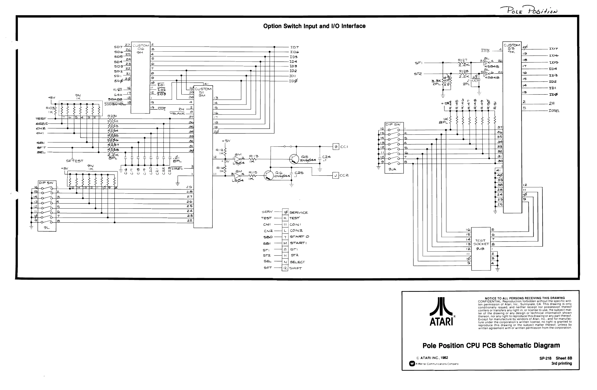
Tiiith Topaens_ S| R231 Option Switch Input and I/O Interface
0/0 |S], aTs] ys
(y Lafcustom sl
Res2
R2s3 R2s4 Poce Poe stian
C B.3K om i 4 con pot 3K Sit rp2 ZPL ont 2PL a -——— rp
RSs Rese yf fff fe Me Ue J Joo fs
BTU] ~]o] so]
confers or transfers any right in, or license to use, the subject mat ter of the drawing or any design or technical information shown
thereon, nor any right to reproduce this drawing or any part thereo!
Except for manufacture by vendors of Atari, Inc., and for manufac:
ture Under the corporation's written license, no right is granted to reproduce this drawing or the subject matter thereof, unless by written agreement with or written permission from the corporation. NOTICE TO ALL PERSONS RECEIVING THIS DRAWING CONFIDENTIAL: Reproduction forbidden without the specific writ: ten permission of Atari, Inc., Sunnyvale, CA. This drawing is only conditionally issued, and neither receipt nor possession thereot
@
Pole Position CPU PCB Schematic Diagram
© ATARI INC., 1982 SP-218 Sheet 8B A were: communcatons Company 3rd printing
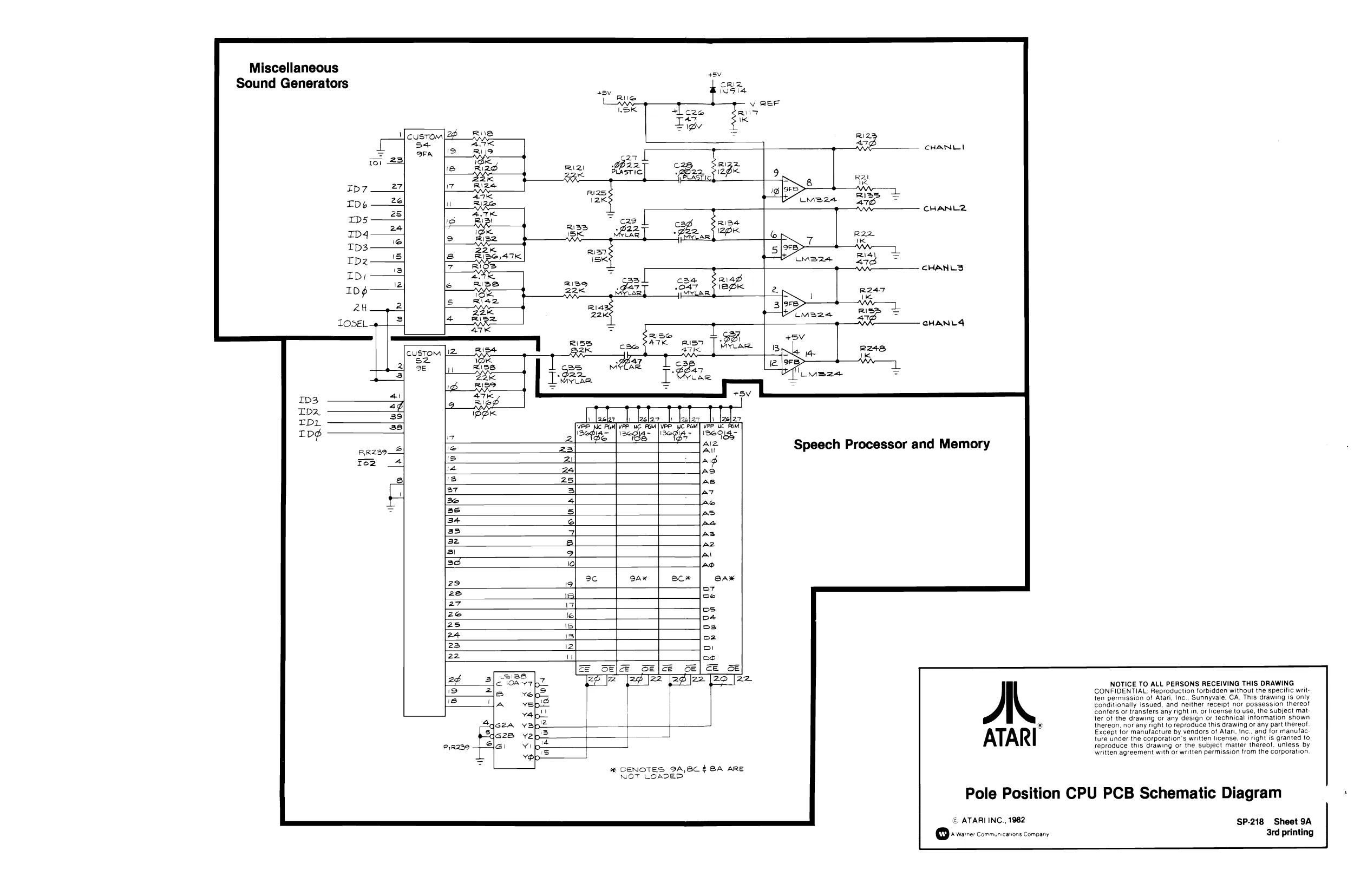
Miscellaneous Sound Generators
custom|2e SYS LT [s+ a4E OFA CHANLI
| cael | 34 | SRiad |
R130
| ga | O47 | 218DK | ||
| He | eee | AAG | oP | a |
5 Rae Ria: 22K
MYLAR Tt ass BRP ass 1%
| custom [2 | St, | RI | oe. | red |
| SZ | VO | T | war | lcs |
| 3E | as | Meta | 3p. |
daa : L8eSe Teitce
| 35] | b | feeler | falas I | Iochar | hs | Loelen |
TEP pe Pol Pvc Pad] VBP e Pan] VPP Ue
| Ip¢é | ; | 2 Sepia | Bepie~ | [odie | [Sees |
a Rie Speech Processor and Memory
confers or transfers any right in, or license to use, the subject mat:
ter of the drawing or any design or technical information shown NOTICE TO ALL PERSONS RECEIVING THIS DRAWING CONFIDENTIAL: Reproduction forbidden without the specific writ: ten permission of Atari, Inc., Sunnyvale, CA. This drawing is only conditionally issued, and neither receipt nor possession thereot
a thereon, nor any right to reproduce this drawing or any part thereot. Except for manufacture by vendors of Atari. Inc.. and for manufac: ture under the corporation's written license. no right is granted to reproduce this drawing or the subject matter thereof. unless by written agreement with or written permission from the corporation % CENOTES 9A,8C ¢ BA ARE NOT LOADED
Pole Position CPU PCB Schematic Diagram
€ ATARI INC., 1982 SP-218 Sheet 9A +2106: Communications Comany 3rd printing
This page is a drawing, shown as the original scan.
This page is a drawing, shown as the original scan.
TT
TI ©.
we
w wee eeee
TF 1D
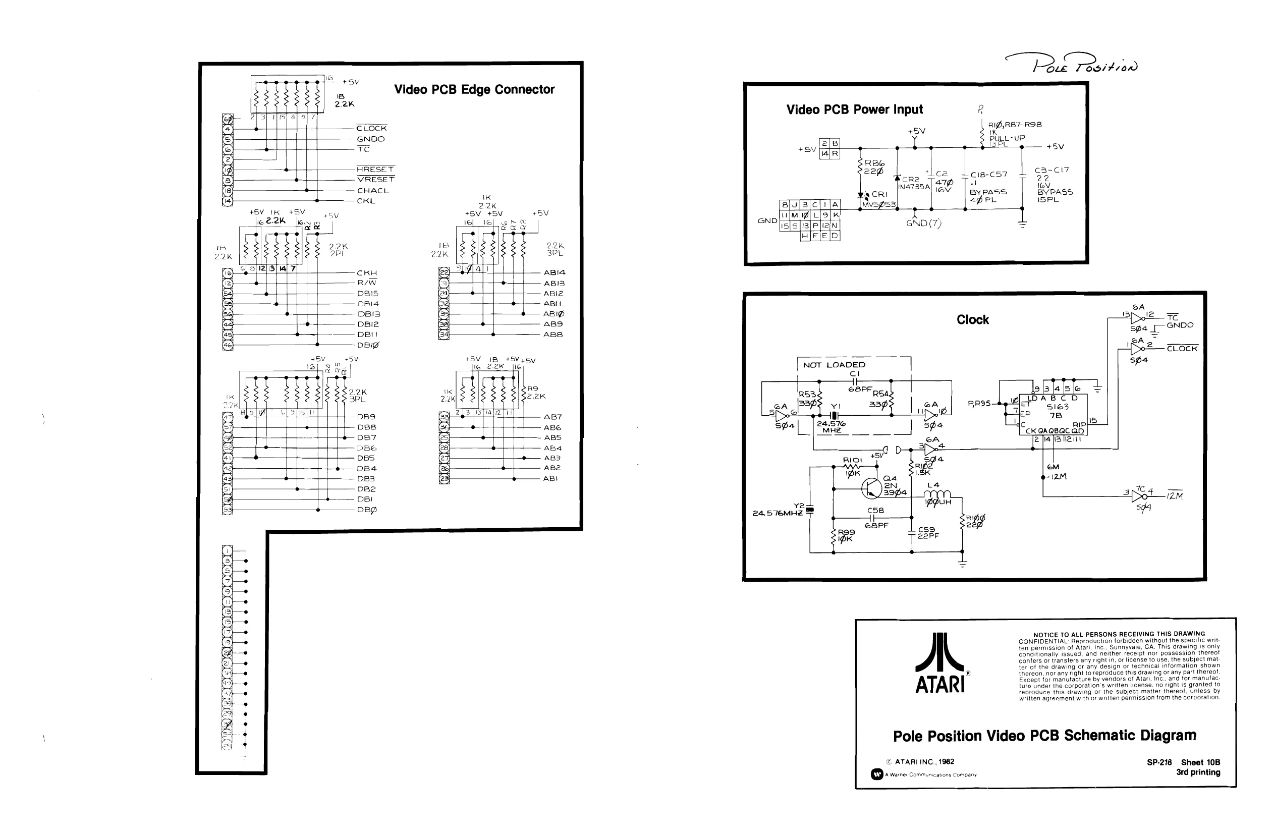
Video PCB Edge Connector
Gj
G
S GNDO fe} . Te B q HRESET 8 VRESET
© - CHACL 4 cKL 25K
| HV IK | HSV | lay | +5V 45V | +8V |
| Wwe22Kh | lew | 16 | 16l | ora |
| - | a | SER |
?
2.2
PPM PERE IANH AB7 . ABE + ~ ABS
——e Aba OOOO0OO! PRE Pesidian
Video PCB Power Input i
Rupe -ve Pie
c1a-C57 al BYPASS agree RIf,RB7-ROB
NOT LOADED
lola +
tee 7B ABCD eT 163
Ic RI ‘CK QAQBGC QD E haps henry
v2
- 576MHE
A
ATARI
eM 12M
3 pe 4 SA
NOTICE TO ALL PERSONS RECEIVING THIS DRAWING CONFIDENTIAL: Reproduction forbidden without the specific writ ten permission of Atari, Inc., Sunnyvale, CA. This drawing is only Conditionally issued, and neither receipt nor possession thereot Confers or transfers any right in, or license to use. the subject matter of the drawing or any design or technical information shown thereon, nor any right to reproduce this drawing or any part thereof. Except for manufacture by vendors of Atari, Inc., and for manufac. ture under the corporation's written license. no right is granted to reproduce this drawing or the subject matter thereof, unless by written agreement with or written permission from the corporation
Pole Position Video PCB Schematic Diagram
© ATARI INC., 1982 SP-218 Sheet 108 3rd printing
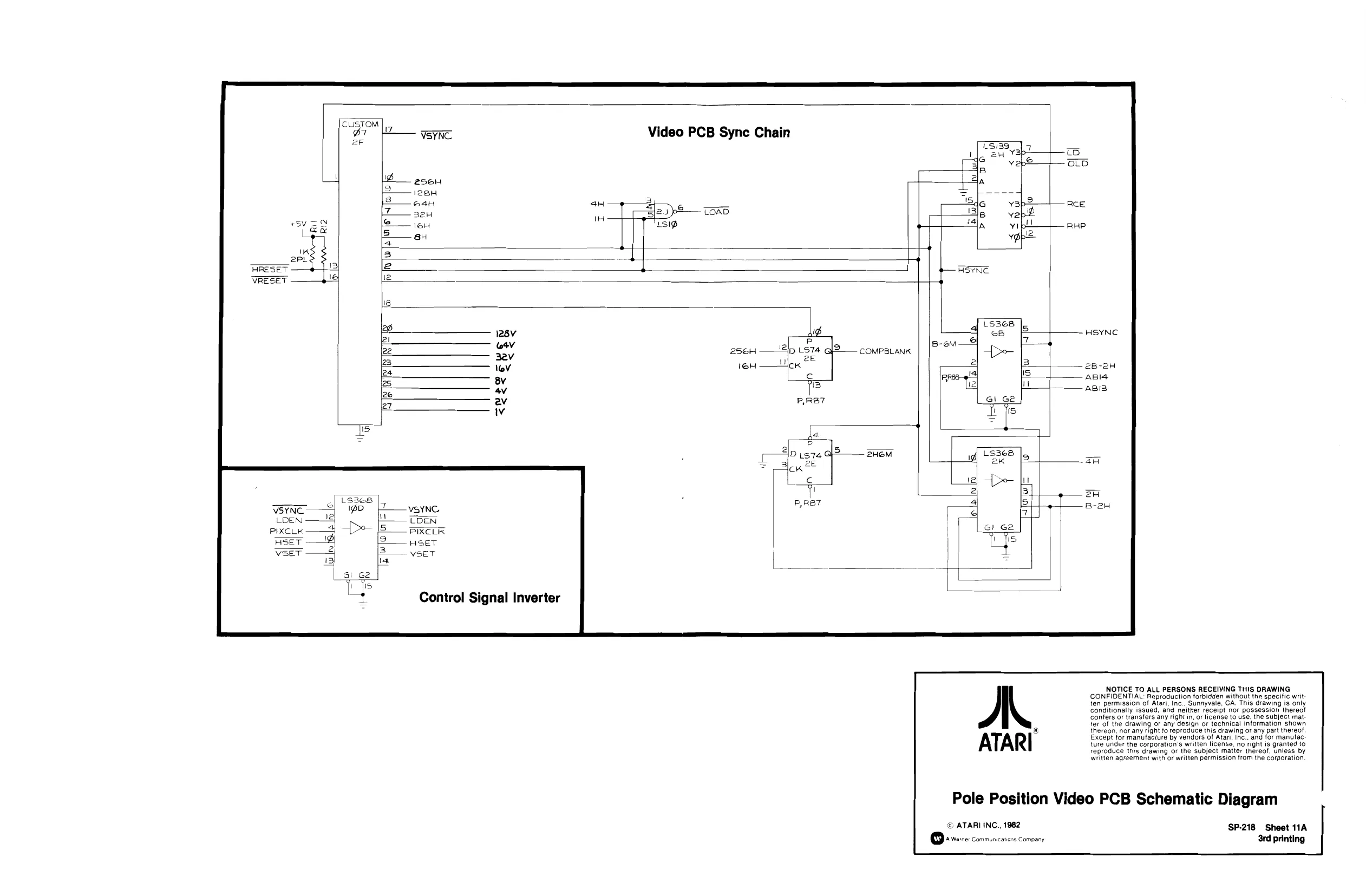
This page is a drawing, shown as the original scan.
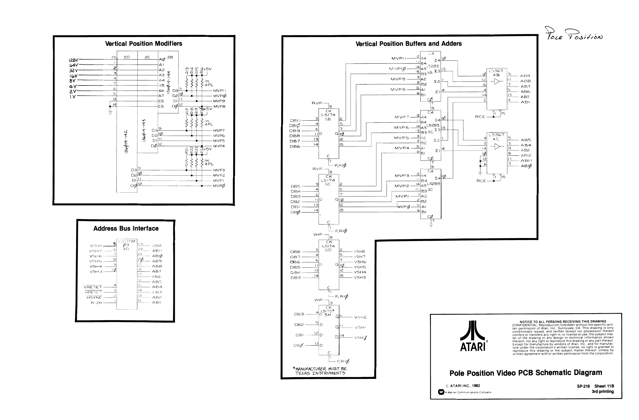
OLe VY oS/47dn Vertical Position Buffers and Adders Vertical Position Modifiers
2D 2c 2B rg Al
Az 1Bepiq- 144
iv} Z
136914 142.
Wo aye fj — MVPI
- + — veg
Address Bus Interface
VRESET
SYNE B-2H
pei ——4/p Confers or transters any right in, or license to use, the subject mat. ter of the drawing or any design or technical information shown
' thereon, nor any right to reproduce this drawing or any part thereot,
Except for manufacture by vendors of Atari, Inc... and for manufac: ture under the corporation's written license. no right is granted to reproduce this drawing or the subject matter thereof, unless by wntten agreement with or written permission from the corporation. NOTICE TO ALL PERSONS RECEIVING THIS DRAWING CONFIDENTIAL: Reproduction forbidden without the specific writ ten permission of Atari, Inc., Sunnyvale, CA. This drawing is only Conditionally issued, and neither receipt nor possession thereot
a
cod ee XMANUFACTURER MUST BE TEXAS INSTRUMENTS
Pole Position Video PCB Schematic Diagram
ATARI INC., 1982 ‘SP-218 Sheet 11B © + Warr: Communications Comoany 3rd printing
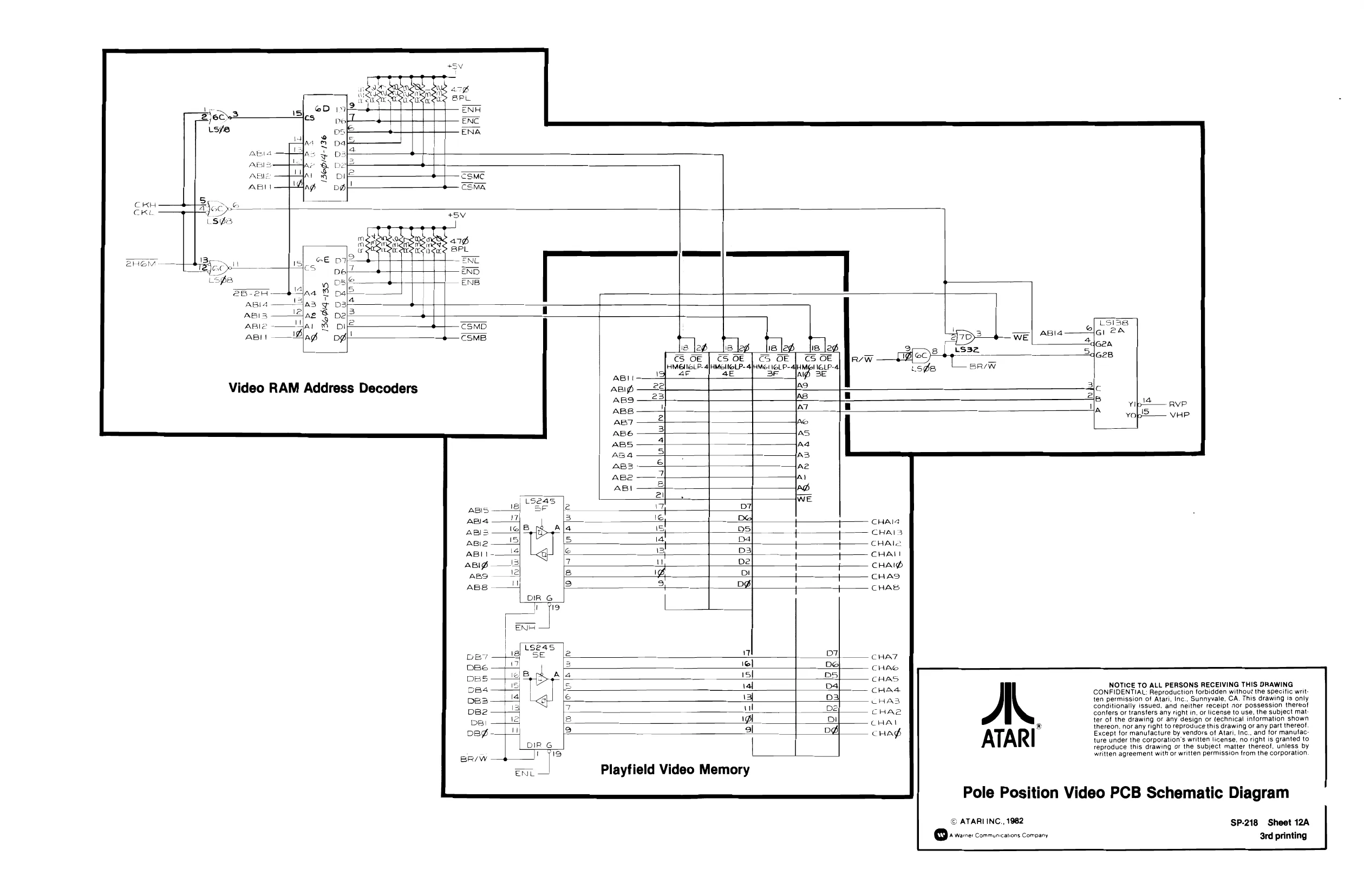
This page is a drawing, shown as the original scan.
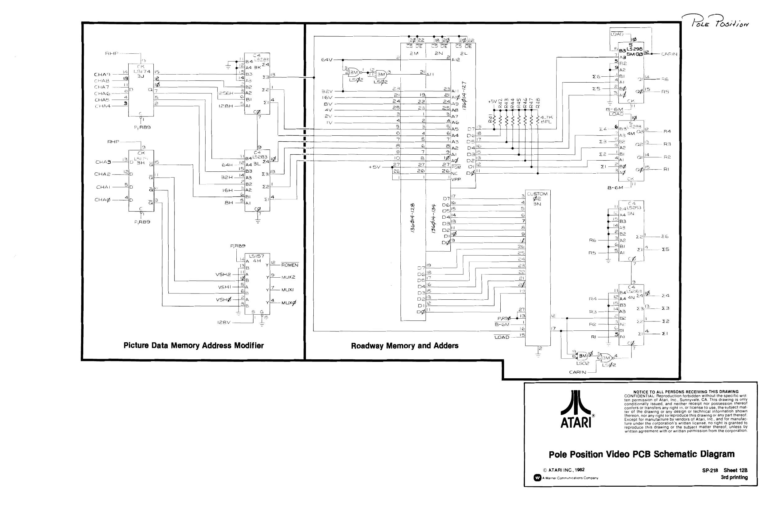
This page is a drawing, shown as the original scan.
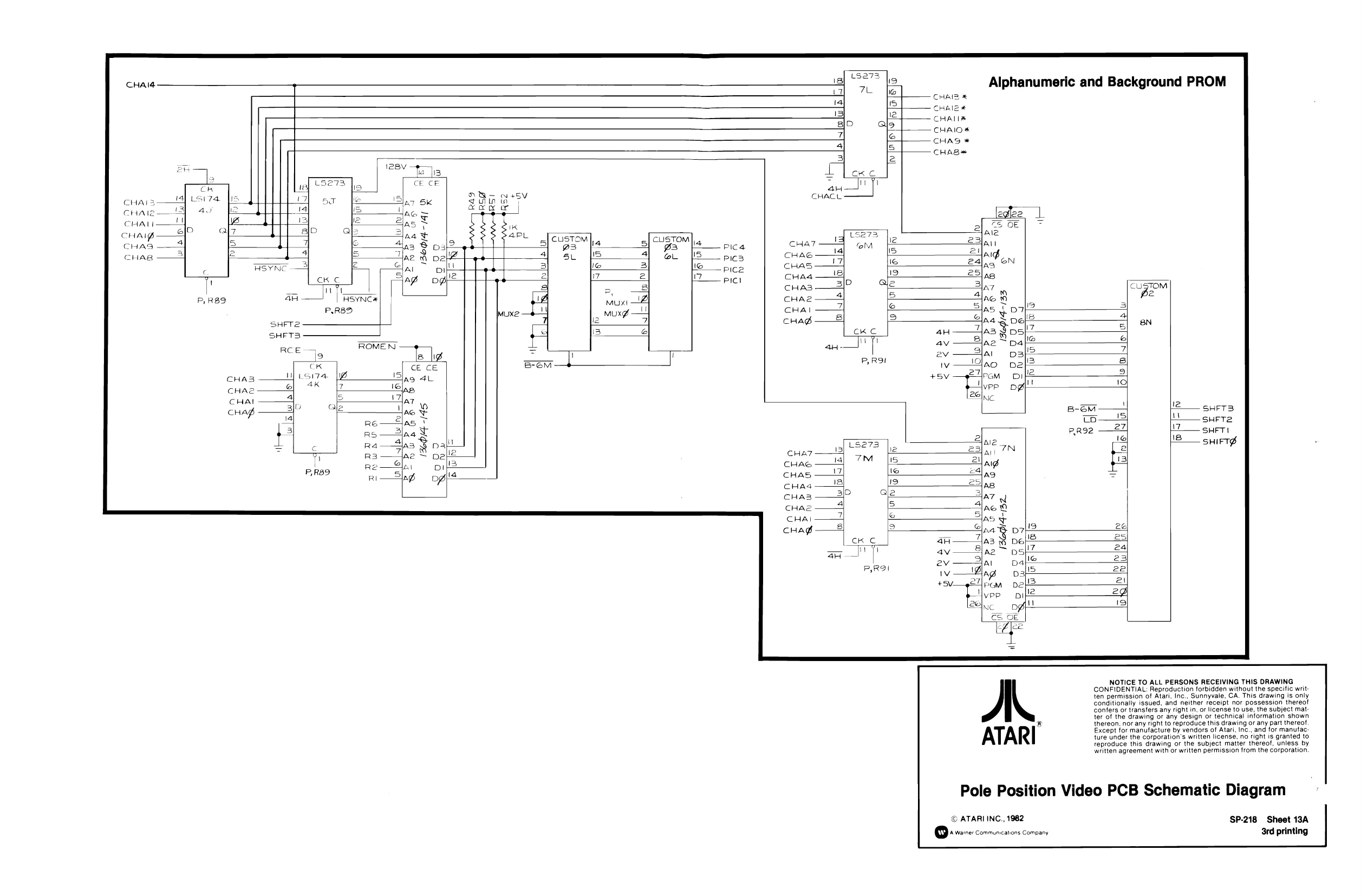
This page is a drawing, shown as the original scan.
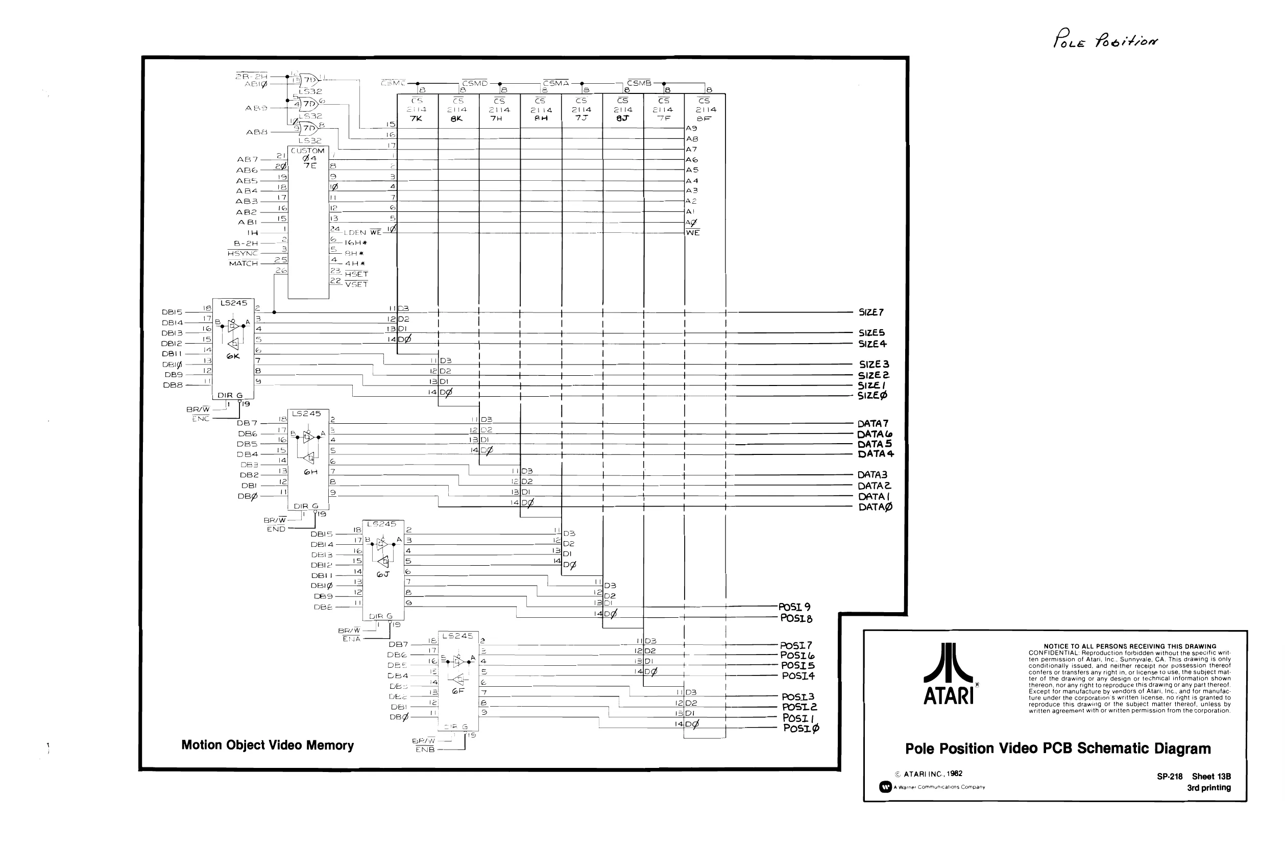
This page is a drawing, shown as the original scan.
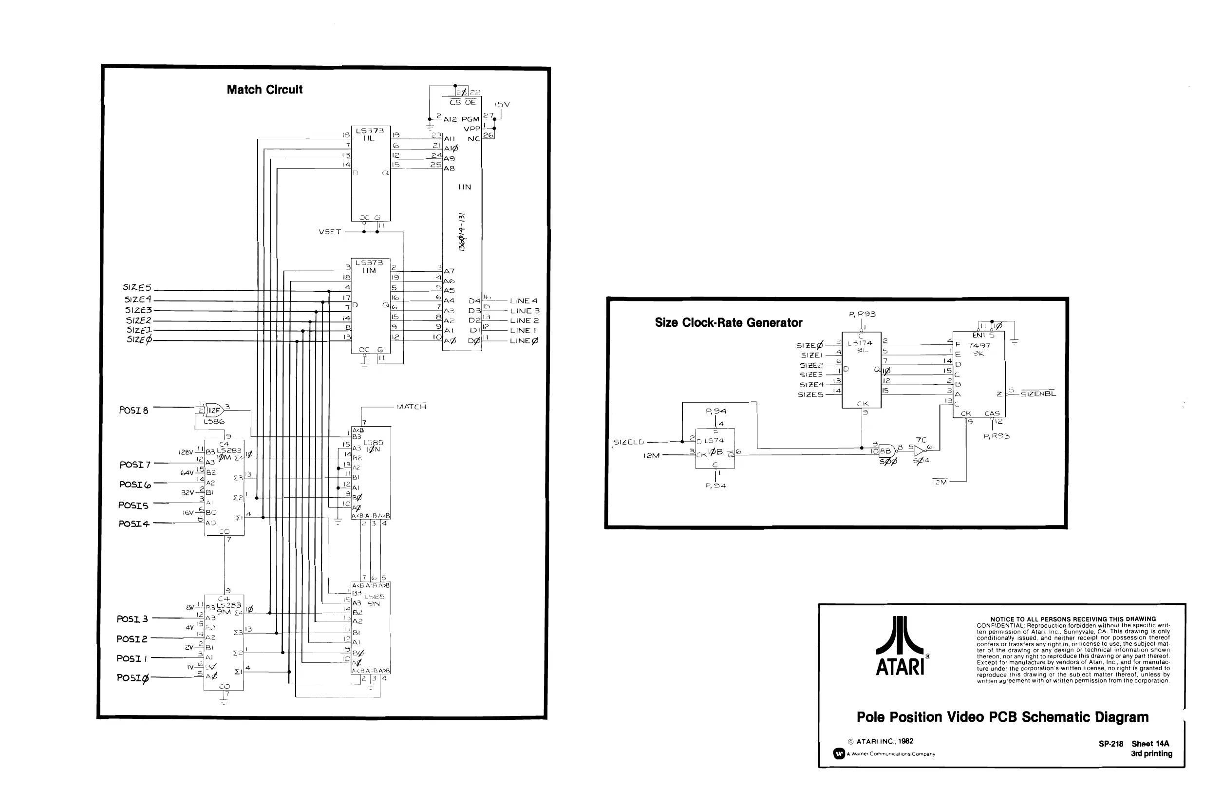
This page is a drawing, shown as the original scan.
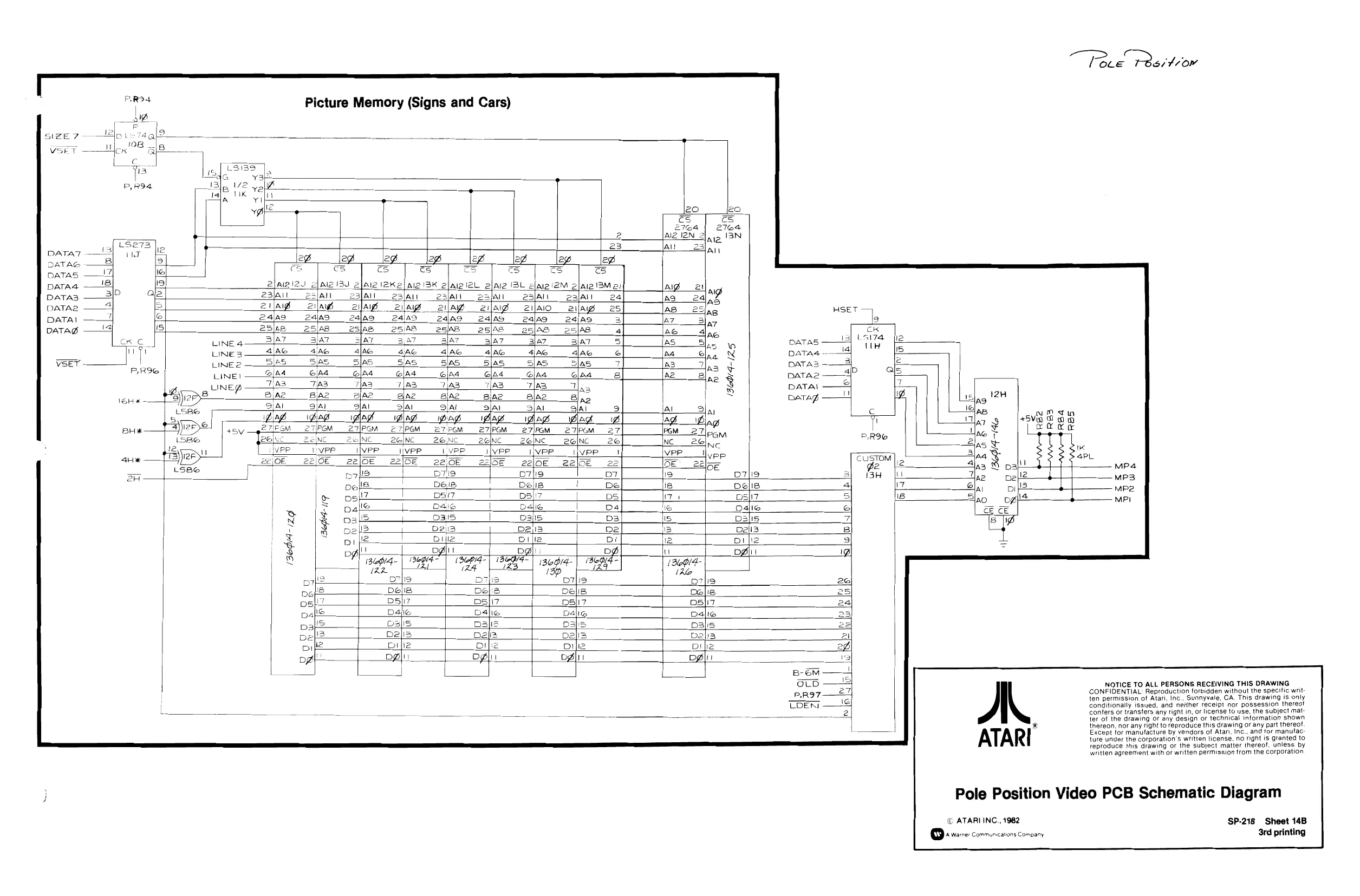
This page is a drawing, shown as the original scan.
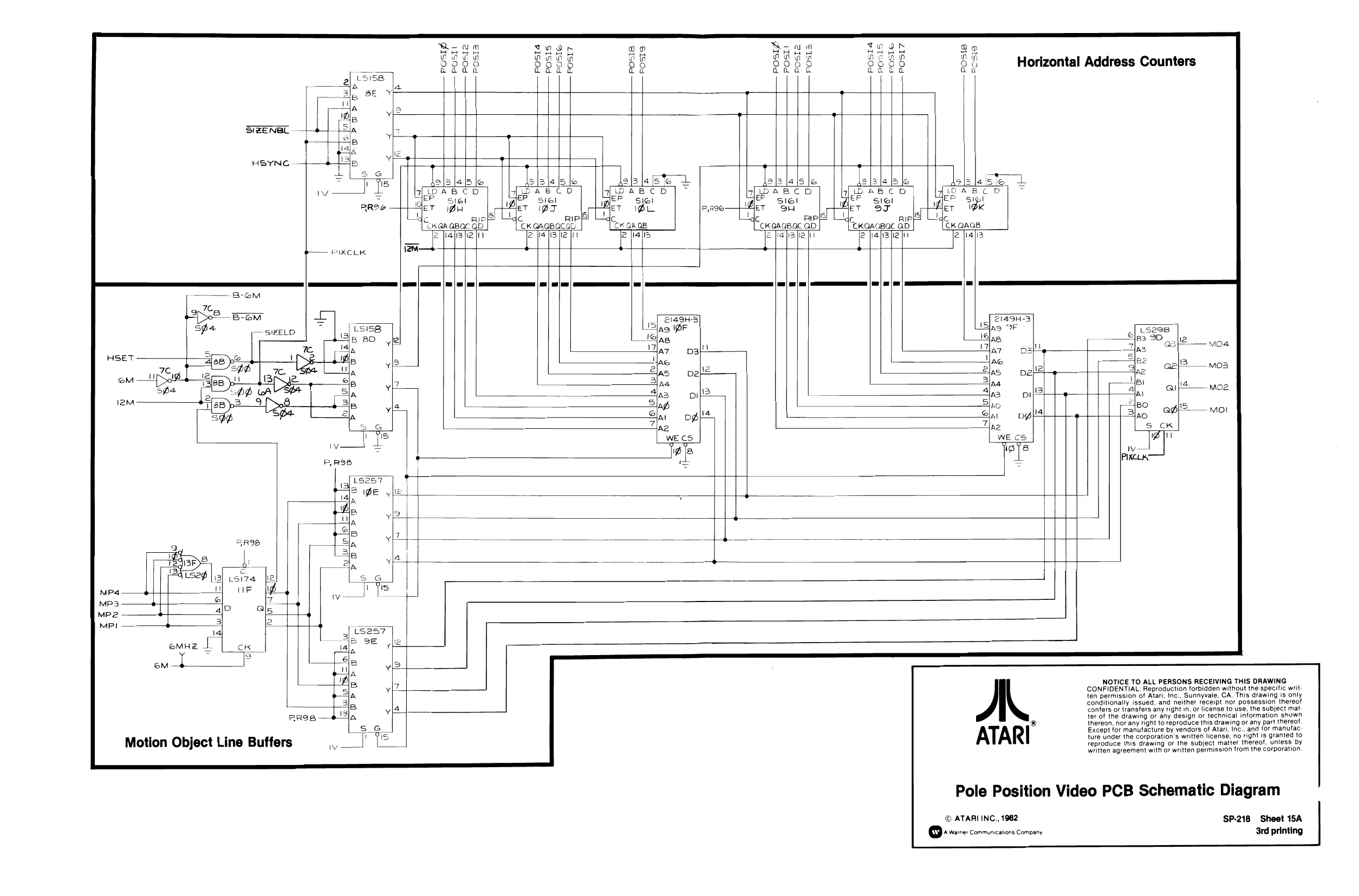
SZENBL
HSYNG POSsI4 POsI5, Posts Posia POSIG
—POSI7
$e PIKCLK
le i lag IDF al Si Horizontal Address Counters
IAT BI
e R safe fons lw fo | Esk |
JO [ur Js [tw Irv
Motion Object Line Buffers
RRIB OS a A.
ATARI
© ATARI INC., 1982
Pole Position Video PCB Schematic Diagram
NOTICE TO ALL PERSONS RECEIVING THIS DRAWING CONFIDENTIAL: Reproduction forbidden without the specitic writ ten permission of Atari, Inc., Sunnyvale, CA. This drawing is only conditionally issued, and neither receipt nor possession thereof conters or transfers any right in, or license to use, the subject mat ter of the drawing or any design or technical intormation shown
thereon, nor any right to reproduce this drawing or any part thereof,
Except for manutacture by vendors of Atari, Inc.. and for manufac. ture under the corporation's written license, no right is granted to feproduce this drawing or the subject matter thereof, unless by written agreement with or written permission from the corporation.
SP-218 Sheet 15A 3rd printing
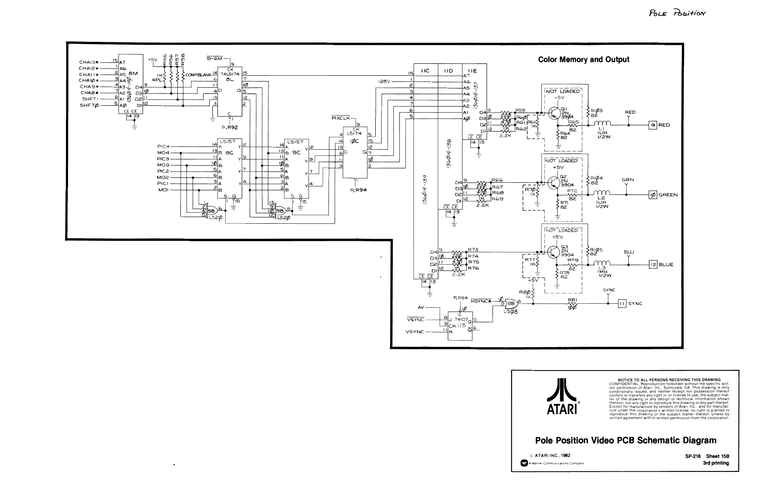
This page is a drawing, shown as the original scan.
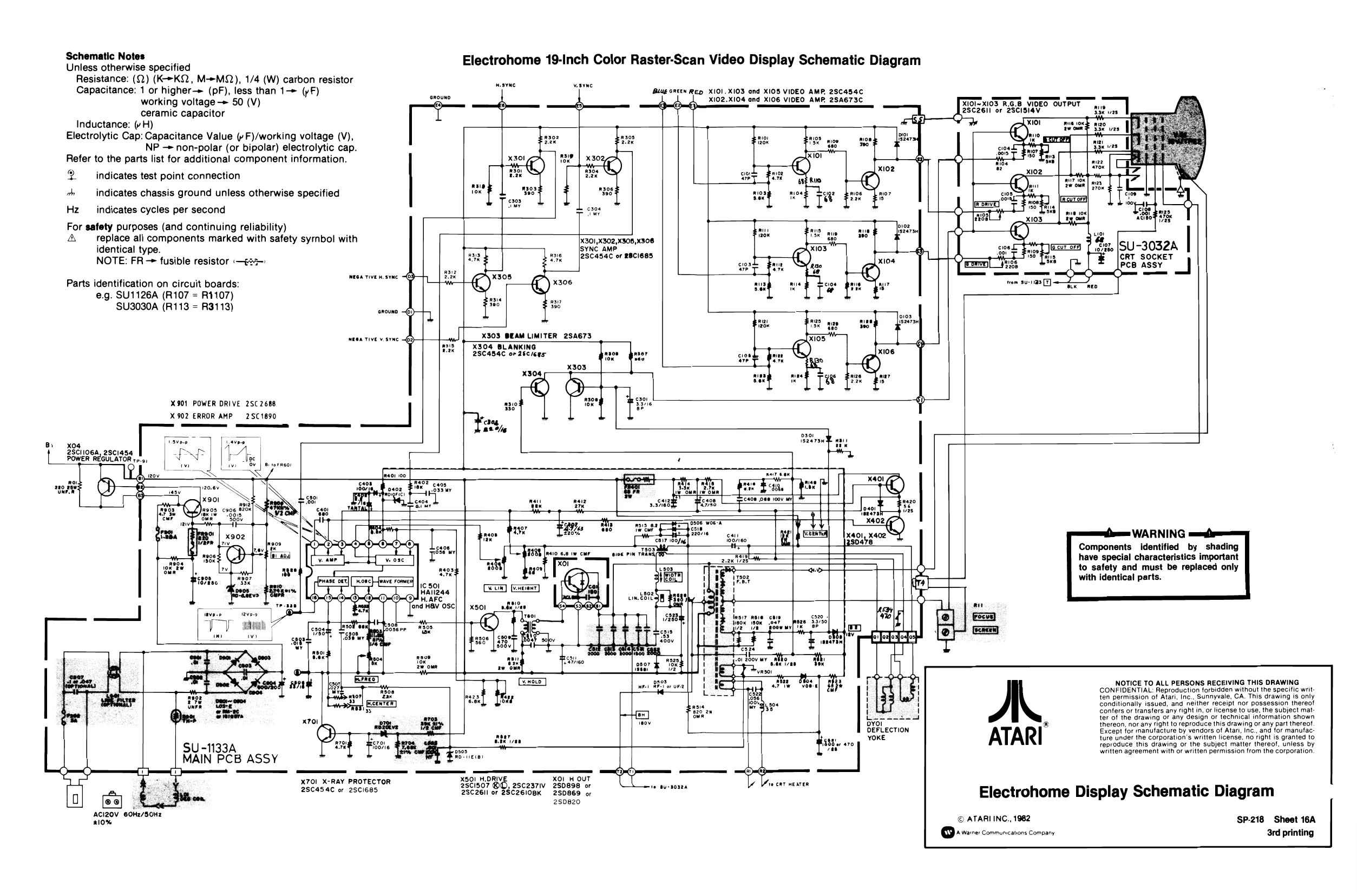
Schematic Notes Unless otherwise specified Resistance: (Q) (K->KQ, M-MQ), 1/4 (W) carbon resistor eevee ceyve Capacitance: 1 or higher-» (pF), less than 1-> (pF) "| " Blug cREEN RED X101.XI03 and XI05 VIDEO AMP, 2SC454c working voltage -» 50 (V) ~~ —_4 a 3-6) ceramic capacitor Inductance: ( H) Electrolytic Cap: Capacitance Value (y F)/working voltage (V), NP non-polar (or bipolar) electrolytic cap. Refer to the parts list for additional component information. | Electrohome 19-Inch Color Raster-Scan Video Display Schematic Diagram
Xl0l~X103 R.G.B VIDEO OUTPUT ,,., 28C26ll or 2SCISI4V. aes Te
|g 1
2 indicates test point connection ane Tox oh indicates chassis ground unless otherwise specified Hz indicates cycles per second For satety purposes (and continuing reliability) AN replace ali components marked with safety syrnbol with X301,X302,X308,x306 identical type. SYNC AMP.
Parts identification on circuit boards: x56, e.g. SU1126A (R107 = R1107) $U3030A (R113 = R3113) aroun
X303 BEAM LIMITER 2SA673 X304 BLANKING 23C484C oF 28c/68s ns0e prior Ton’ Wise X303 x304
X901 POWER DRIVE 2S 2686 net X 902 ERROR AMP 251890 | —— ‘choy. ate
x04 2Scil06a, 2sci4sq
POWER REGULATOR rp,
nay san, Ean Ecce pe8 100 a on nee nx
me Pe
{ 188% [roo oo w cur Pry : m0 ae) ai (Cece) Eenerent)
2.20 gm
even ; ee)
co w i cara
r NOTICE TO ALL PERSONS RECEIVING THIS DRAWING t CONFIDENTIAL: Reproduction forbidden without the specific writ i t ten permission of Atari, Inc., Sunnyvale, CA. This drawing is only Conditionally issued, and neither receipt nor possession thereof! Confers or transfers any right in, or license to use, the subject mat- RereleS ter of the drawing or any design or technical information shown Ovo! ' thereon, nor any right to reproduce this drawing or any part thereof. DEFLECTION Except for manufacture by vendors of Atari, Inc., and for manufac: YOKE ture under the corporation's written license, no right is granted to reproduce this drawing or the subject matter thereof, unless by written agreement with or written permission trom the corporation SU -1133A MAIN PCB ASSY
- X50! H.DRIVI XO1_H OUT ¢ i RTO! A RAY PROTECTOR 28CI507 OO, 2sc237iv 280898 or te aveaoaza ne-EaT WERTER 28C454C or 25ci685 28C26Il or 2SC2610BK 20869 or 280820
Electrohome Display Schematic Diagram
ey acreoe GOHz/SOHz © ATARI INC., 1962 SP-218 Sheet 16A Qrvere: Communications Company 3rd printing
Fece Foss tion
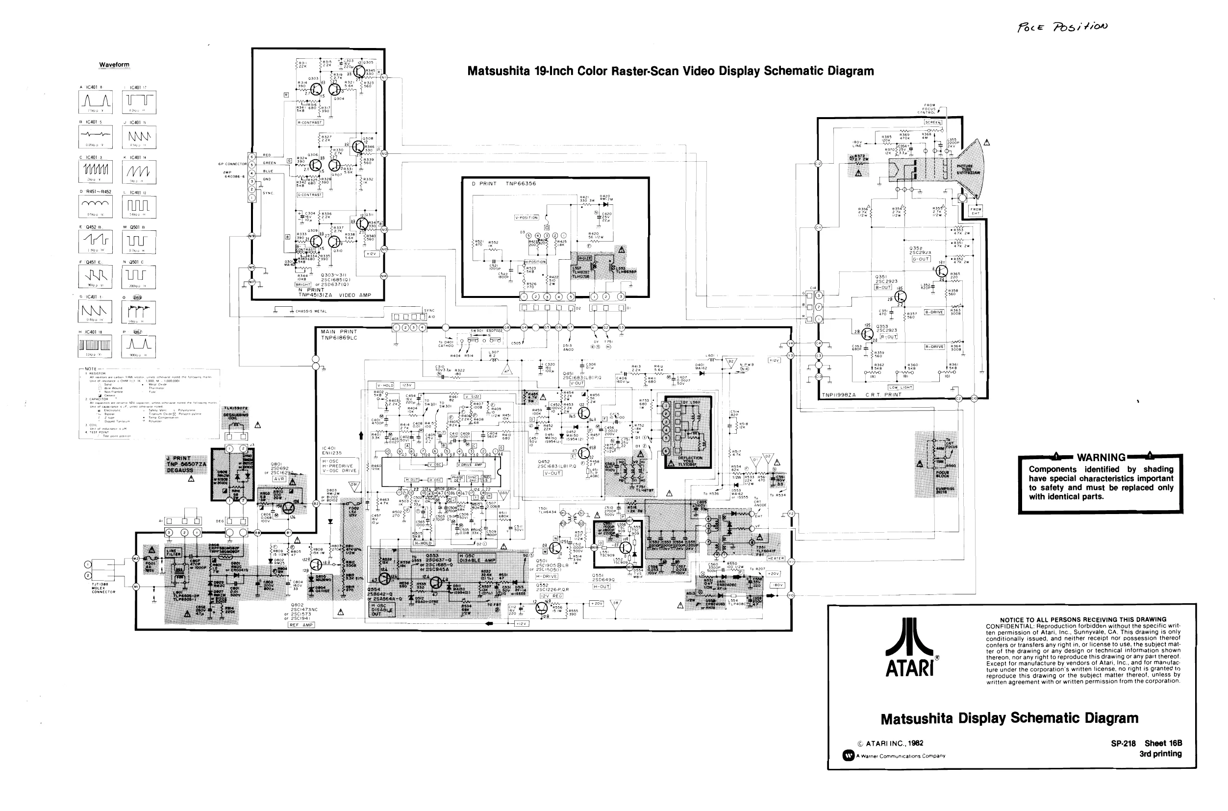
Waveform wees Matsushita 19-Inch Color Raster-Scan Video Display Schematic Diagram
AAl [TF]
eas gs aae te D PRINT TNP6G356 9 RASI~REB? Joan
Foie
mye” gzoxcau | a [pcr ox Sebearish NPR sca Tueagisiza VIDEO Ame
WAIN PRINT h 1c40r TNP6IB69LC ba me |
CRT PRINT TNPN99828, aoe haa BT ao 295 BY, oe: ag
= \7 or 8ciaar [er awe) NOTICE TO ALL PERSONS RECEIVING THIS DRAWING CONFIDENTIAL: Reproduction forbidden without the specitic writ: ten permission of Atari, Inc., Sunnyvale, CA, This drawing is only conditionally issued, and neither receipt nor possession thereof confers or transfers any right in, oF license to use, the subject matter of the drawing or any design or technical information shown thereon, nor any right to reproduce this drawing or any part thereof, Except for manufacture by vendors of Atari, Inc., and for manufac. ture under the corporation's written license. no right is granted to reproduce this drawing or the subject matter thereof, unless by written agreement with or written permission from the corporation.
Matsushita Display Schematic Diagram
© ATARI INC., 1982 SP-218 Sheet 16B A 3rd printing Warnes Communications Company