Gravitar SP-206 1st Printing
Gravitar (version 3) (Atari, 1982) · Schematic Package · 24 pages · 75 sections · original scan
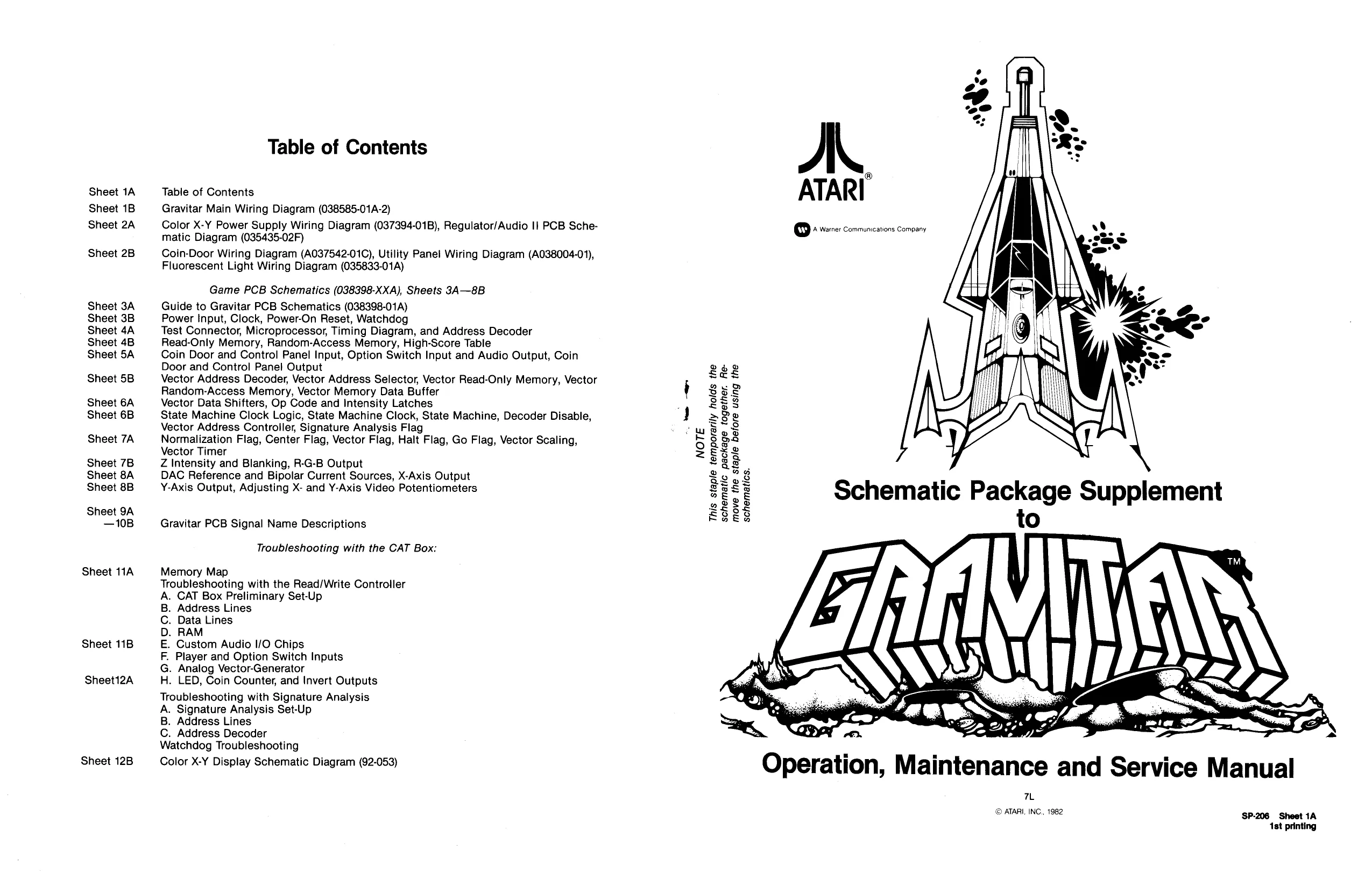
Table of Contents
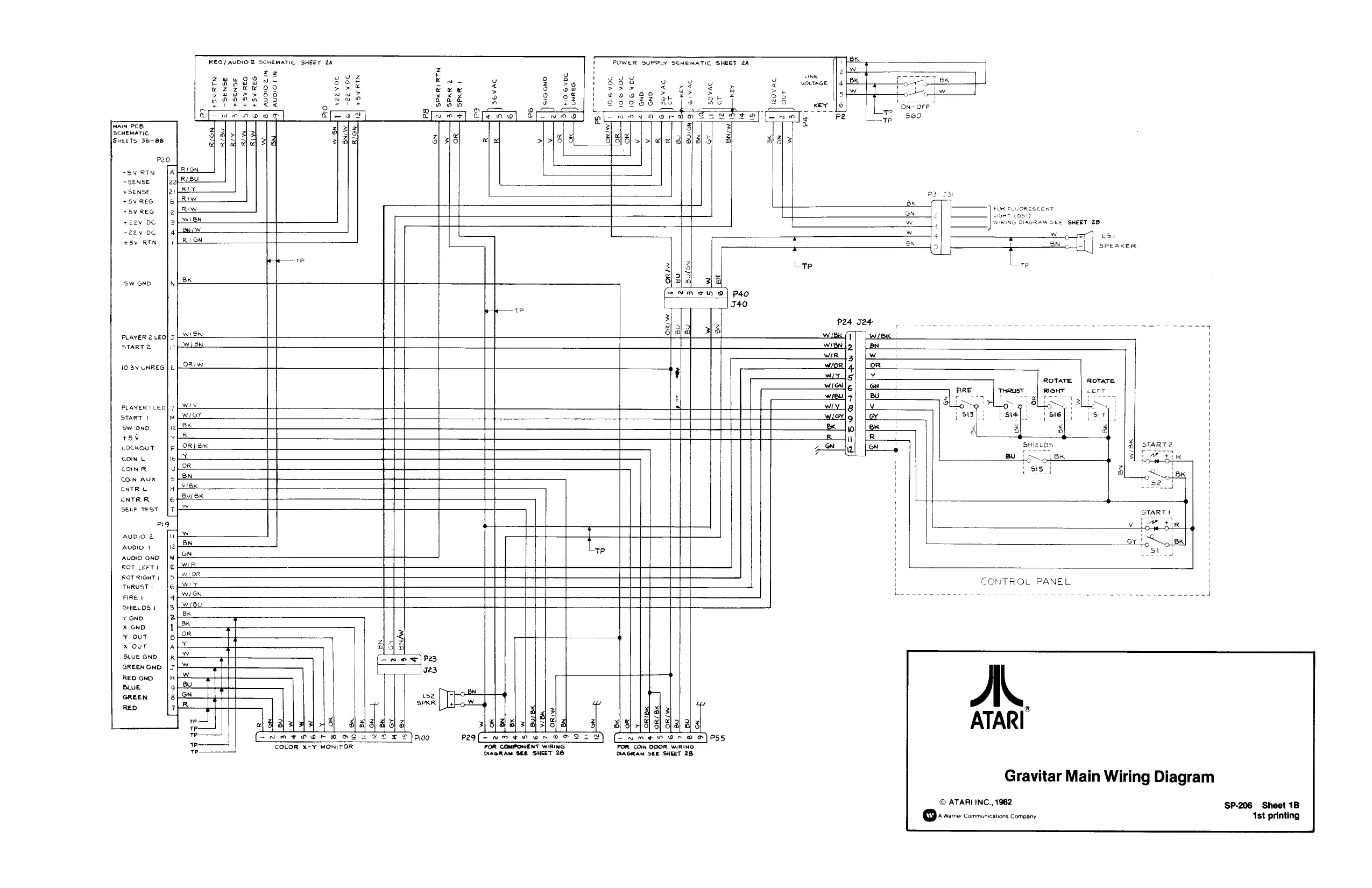
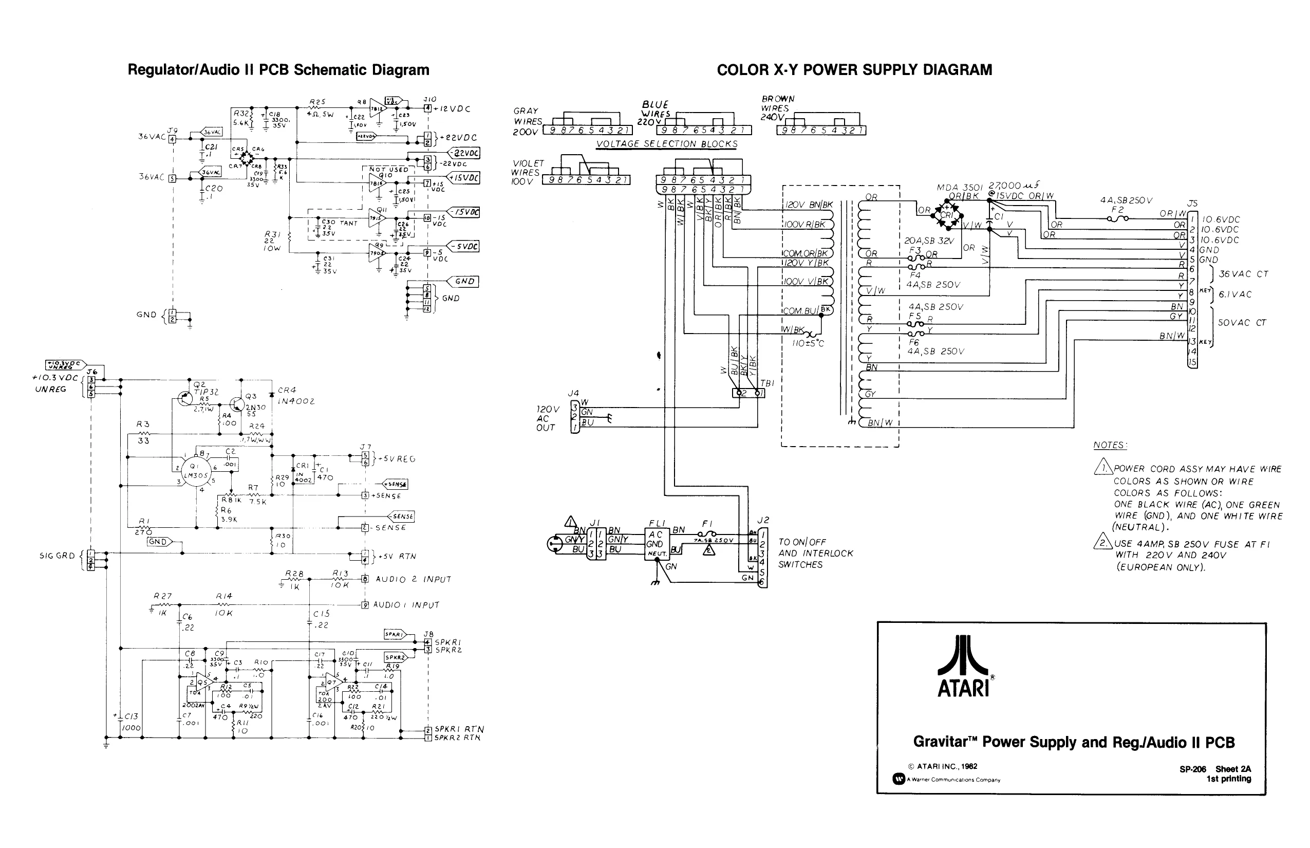
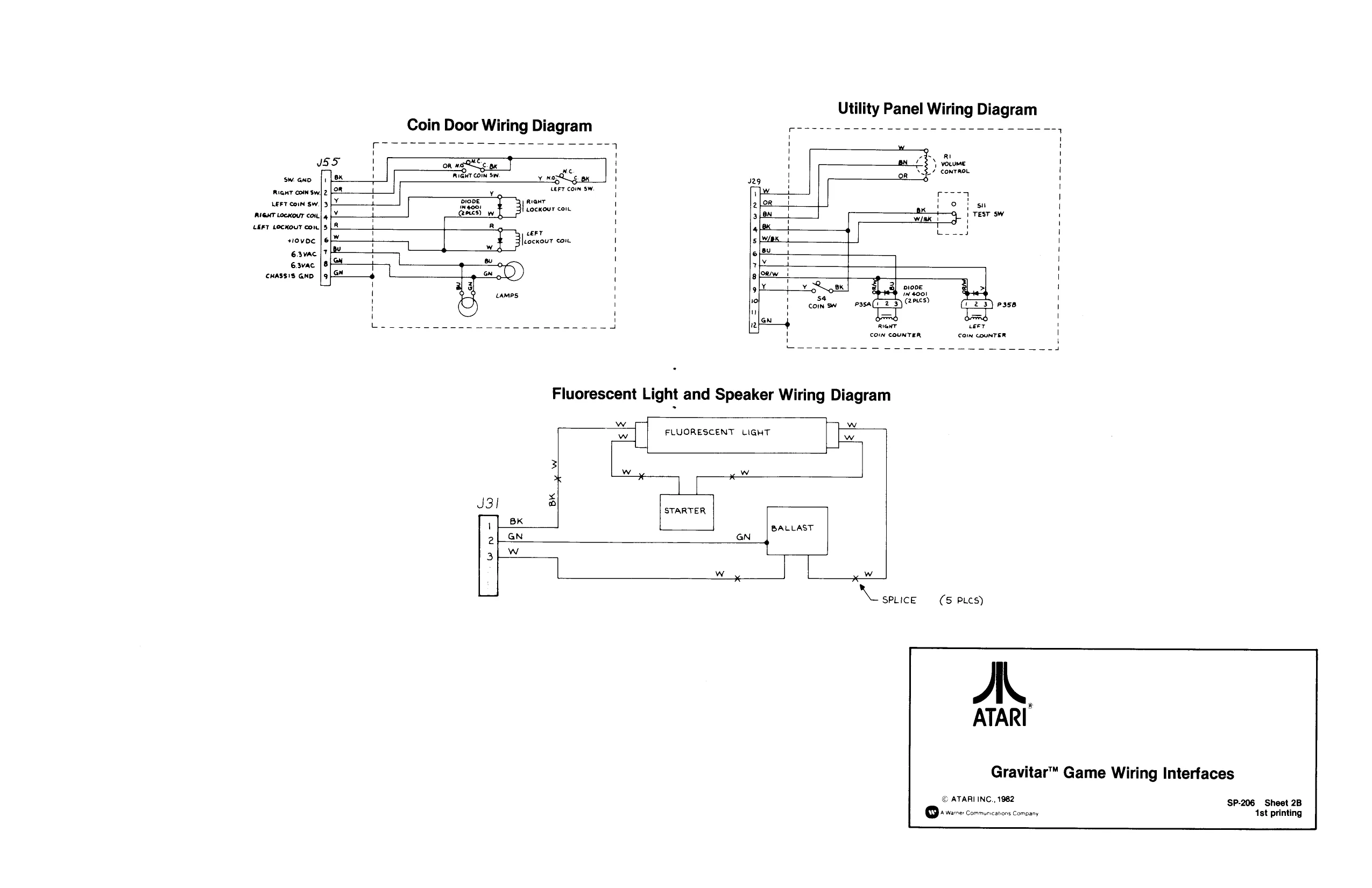
Sheet 1A Table of Contents Sheet 1B Gravitar Main Wiring Diagram (038585-01A-2) Sheet 2A Color X-Y Power Supply Wiring Diagram (037394-01B), Regulator/Audio Il PCB Schematic Diagram (035435-02F) Sheet 2B Coin-Door Wiring Diagram (A037542-01C), Utility Panel Wiring Diagram (A038004-01), Fluorescent Light Wiring Diagram (035833-01A)
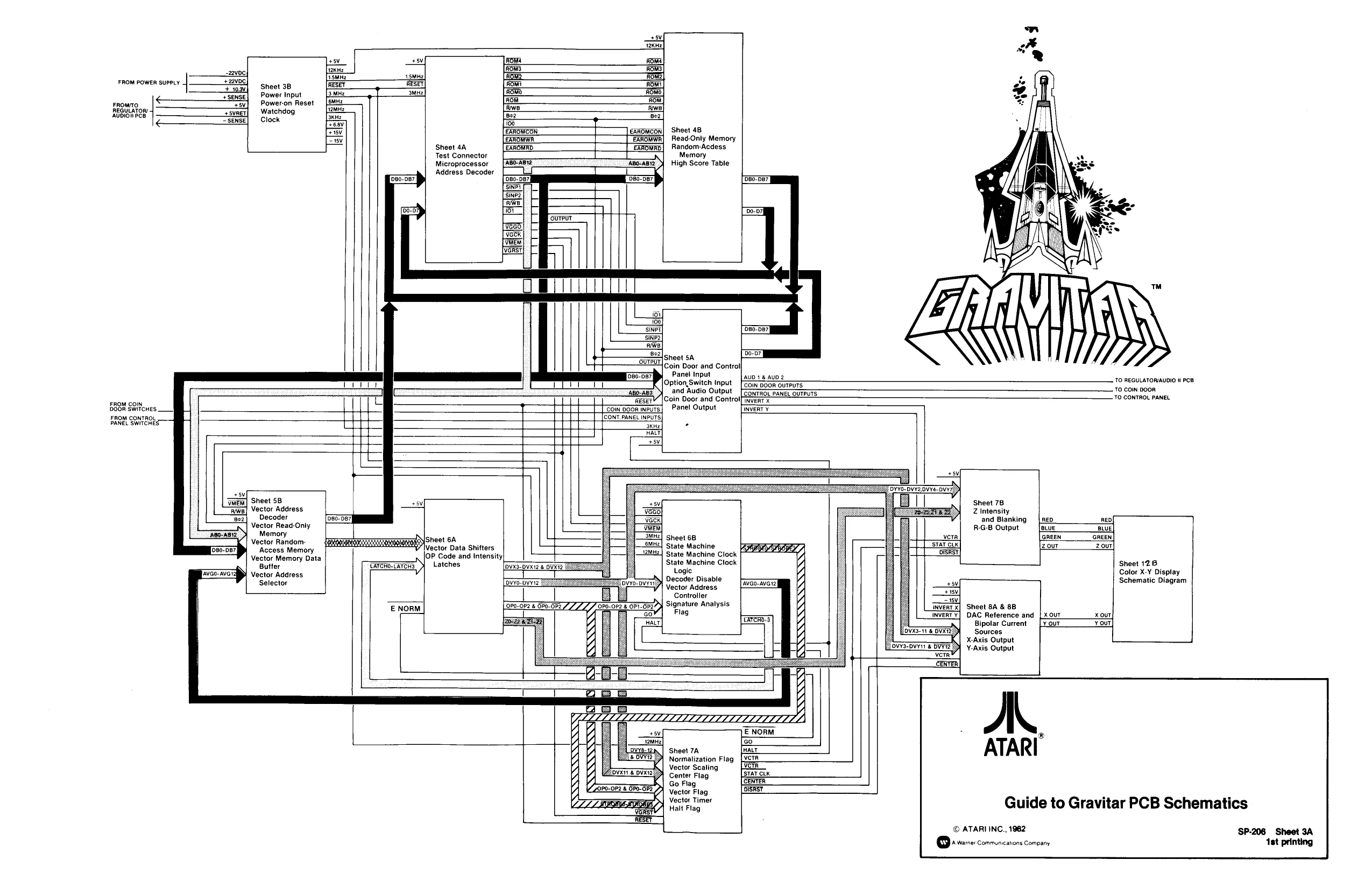
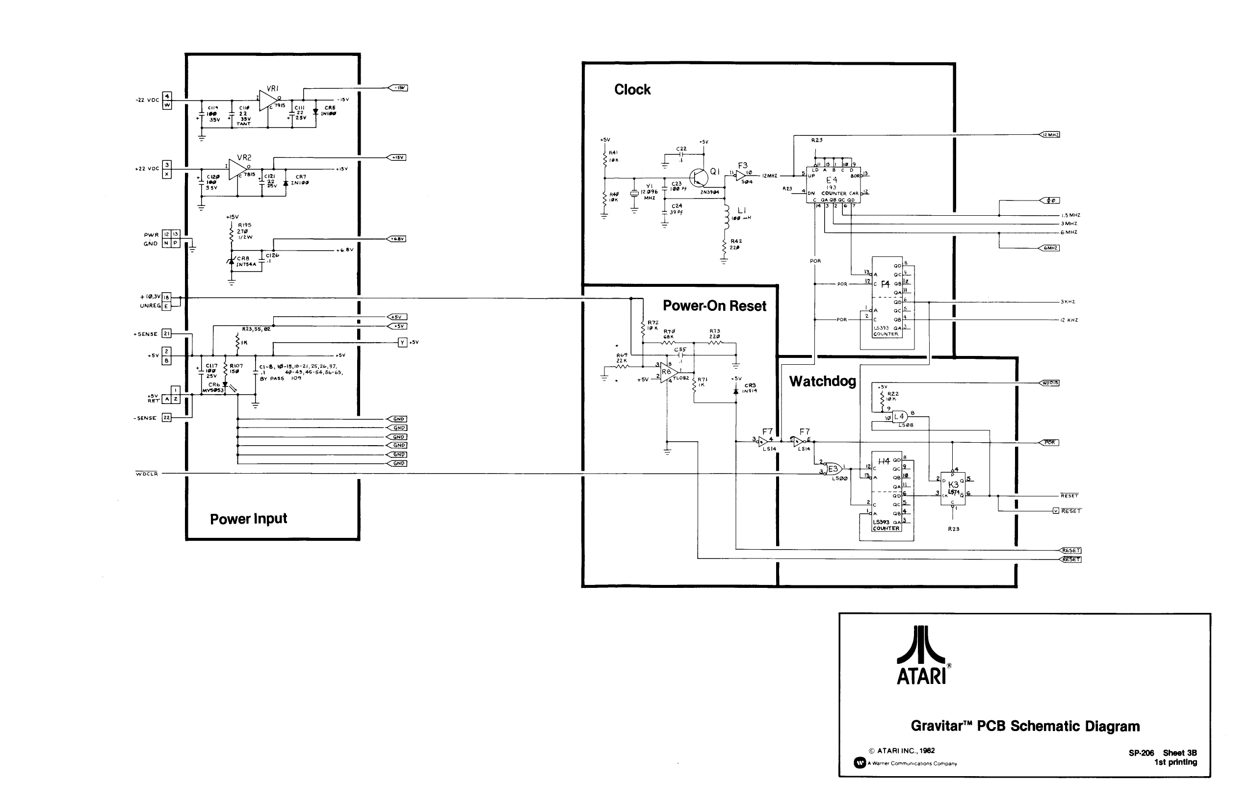
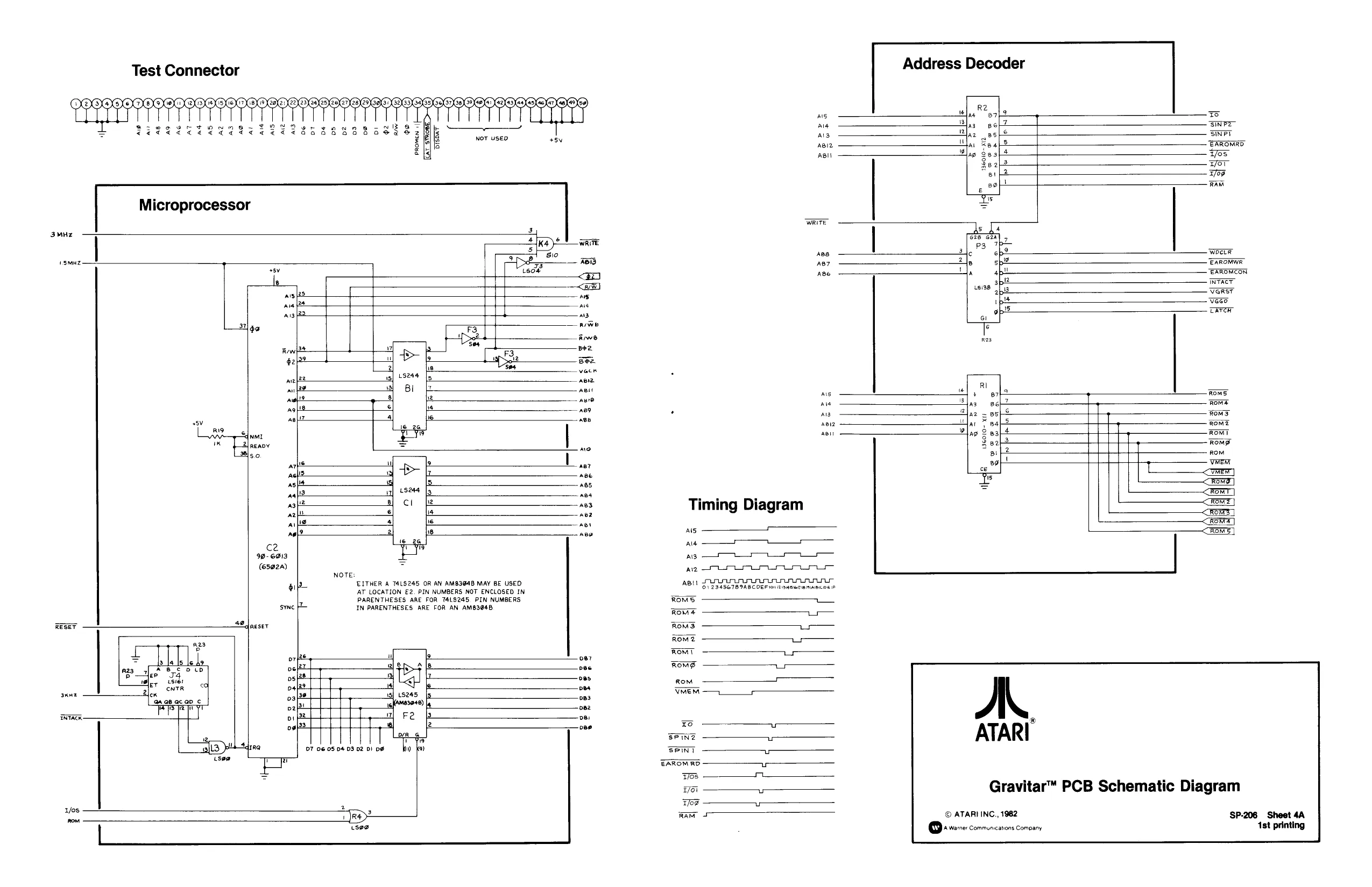
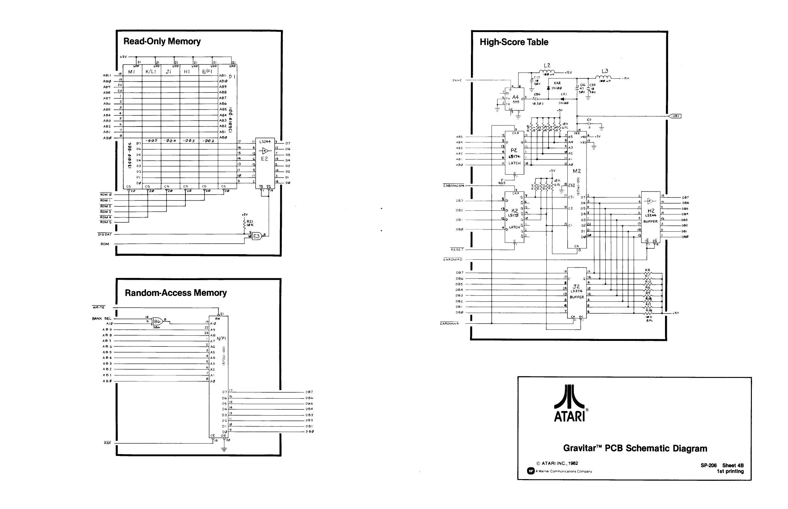
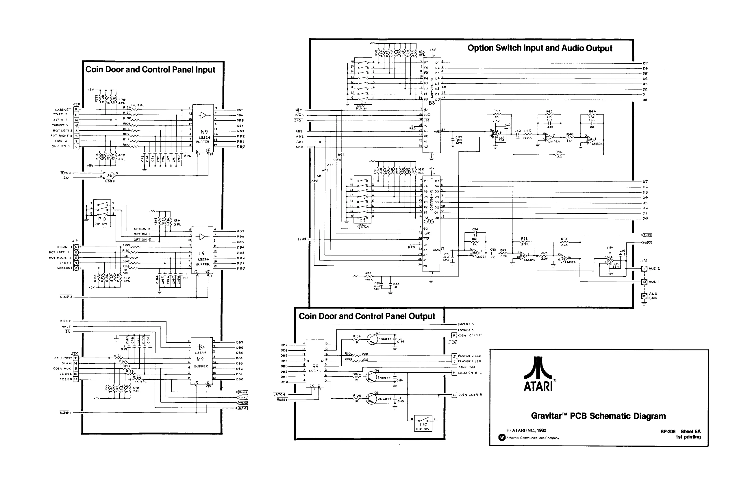
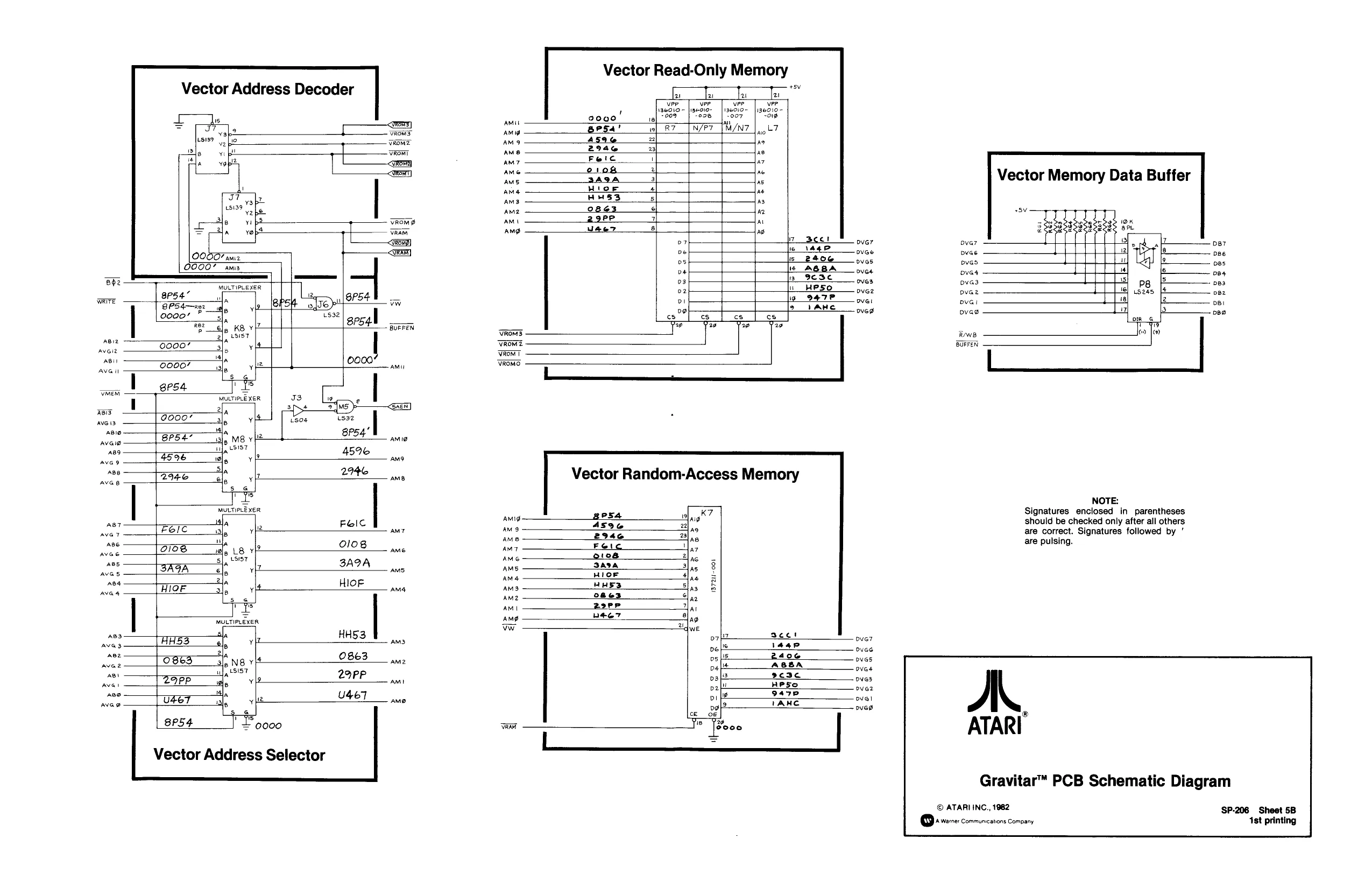
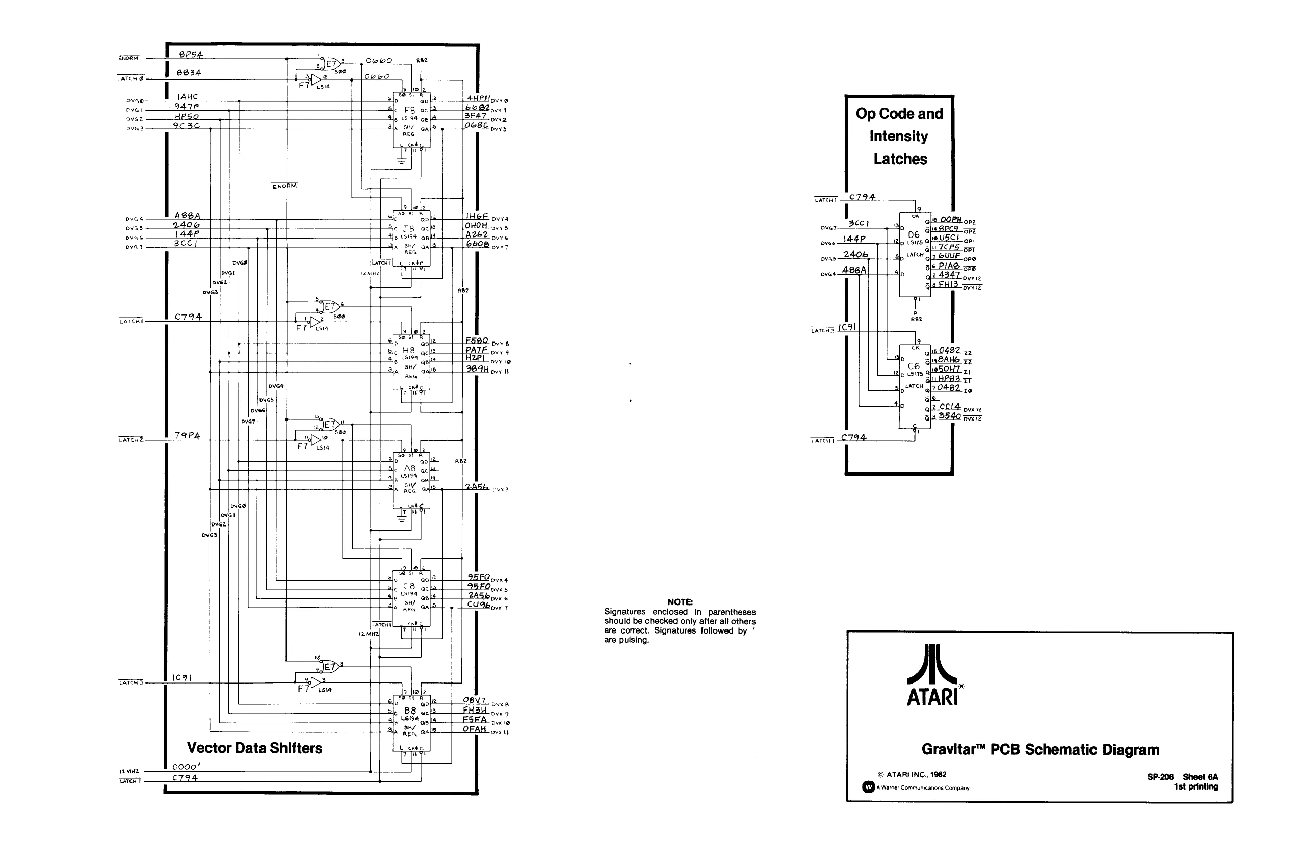
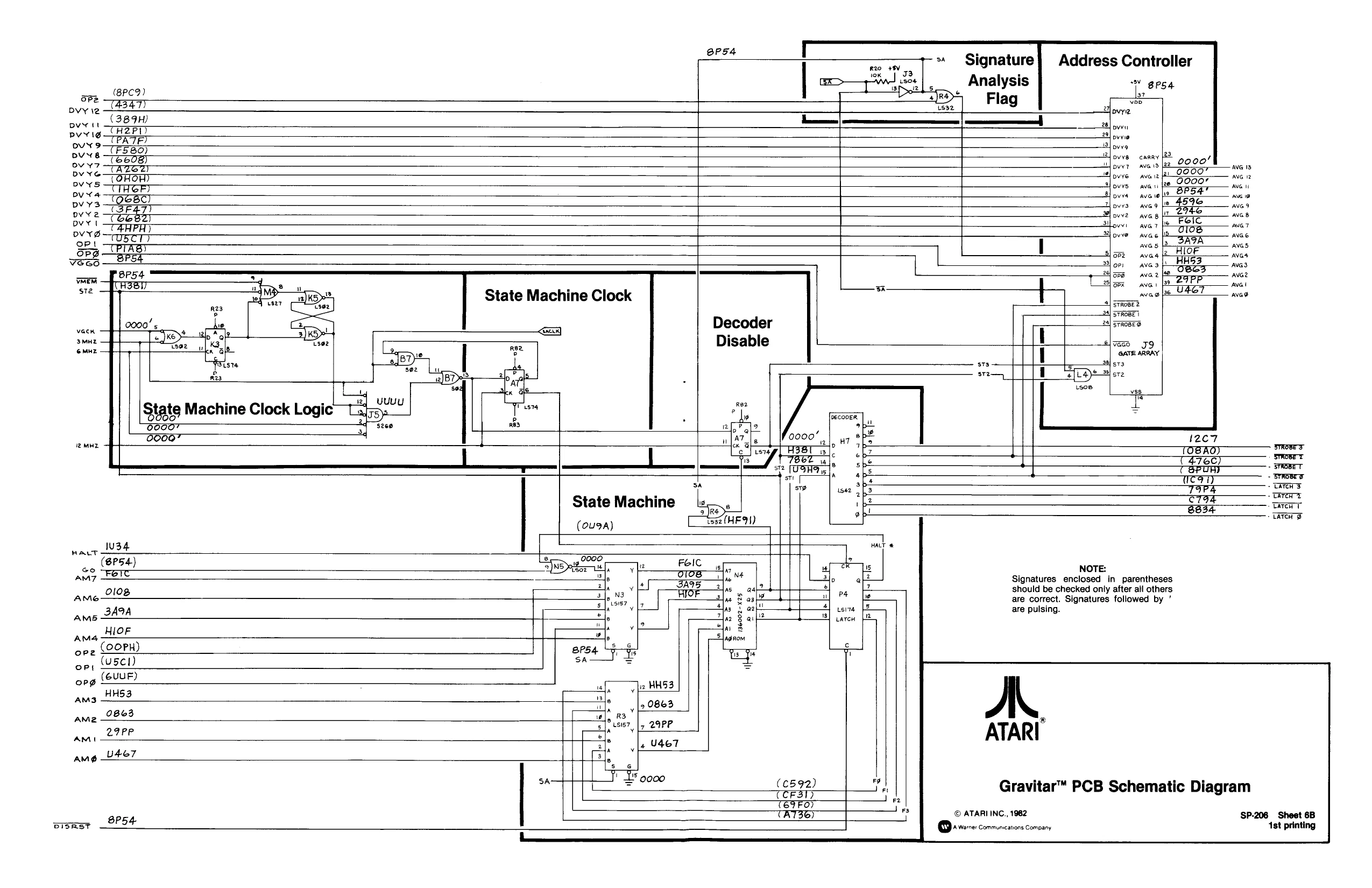
Game PCB Schematics (038398-XXA), Sheets 3A—8B Sheet 3A Guide to Gravitar PCB Schematics (038398-01A) Sheet 3B Power Input, Clock, Power-On Reset, Watchdog Sheet 4A Test Connector, Microprocessor, Timing Diagram, and Address Decoder Sheet 4B Read-Only Memory, Random-Access Memory, High-Score Table Sheet 5A Coin Door and Control Panel Input, Option Switch Input and Audio Output, Coin Door and Control Panel Output Sheet 5B Vector Address Decoder, Vector Address Selector, Vector Read-Only Memory, Vector Random-Access Memory, Vector Memory Data Buffer ' Sheet 6A Vector Data Shifters, Op Code and Intensity Latches Sheet 6B State Machine Clock Logic, State Machine Clock, State Machine, Decoder Disable, ! Vector Address Controller, Signature Analysis Flag : Sheet 7A Normalization Flag, Center Flag, Vector Flag, Halt Flag, Go Flag, Vector Scaling, Vector Timer Sheet 7B Z Intensity and Blanking, R-G-B Output Sheet 8A DAC Reference and Bipolar Current Sources, X-Axis Output Sheet 8B Y-Axis Output, Adjusting X- and Y-Axis Video Potentiometers
Sheet 9A —10B Gravitar PCB Signal Name Descriptions move the staple before using the
schematics.
Troubleshooting with the CAT Box:
Sheet 11A Memory Map Troubleshooting with the Read/Write Controller . CAT Box Preliminary Set-Up . Address Lines Data Lines RAM . Custom Audio I/O Chips Player and Option Switch Inputs . Analog Vector-Generator LED, Coin Counter, and Invert Outputs Troubleshooting with Signature Analysis A. Signature Analysis Set-Up B. Address Lines C. Address Decoder Watchdog Troubleshooting Sheet 128 Color XY Display Schematic Diagram (92.053) Operation, Maintenance and Service Manual
7L © ATARI, INC., 1982 Sheet 11B ronmoom> Sheet12A
SP-206 Sheet 1A
This page is a drawing, shown as the original scan.
This page is a drawing, shown as the original scan.
This page is a drawing, shown as the original scan.
suf | “KH
+5 sv
-z2v06
Power Input
| FRowto | Power-on Reset | fais |
| REGULATOR | Watehdc | ccna |
| Aubioitrce | bila | SKM |
ry jexcrd Sheet 48 =v Read-Only Memory Sheet 4A Random-Acdess Test Connector Memory
Microprocessor High Score Table
Address Decoder
[Sheet 5A [Coin Door and Control} [586-Dar By. Panel Input AUD 18 AvD2
| lOption,Switch input | [Som-abomconnaTS | TO REGULATORIAUDIO M PCB |
and Audio Output AOL PANEL OUTPUTS 70 CoN B00R
| nom con | FeV | |coin Door and Control Sate 7 | v | TO CONTROL PANEL |
| DOOR SwiTcHES, | CONOR NPUTS| | Panel Output | INVERT |
FROM CONTROL, [EONT.PANEL INPUTS| PANEL Swircnes ae : HALT +5
| Sheet 58 | su | | | +s] | Sheet 78 | |||
| Vector Address | Vaao) | Z Intensity | |||||
| Verne | eee Gah | wack] | and Blanking | {neo | neo | ||
| Merno at | Only | wen] | R-G-B Output | fauve | BLUE] | ||
| 4 Vector Random: | Sheet 6A. | 3M] Sheet 6B | vera | GREEN | GREEN | ||
| ‘Access Memory | | | Vector Data Shifters | SE State Machine | ‘STAT CLK] | [z our, | Zour, | |
| Vector Memory Data | OP Code and Intensity | : | State Machine Clock | Sissi] | |||
| S| | Butter | THCHCLATER | Latches | Due | ova 8 OWE | State Machine Clock | Sheet 126 |
| Vector Address | wee: — | Color X-Y Display | |||||
| Selector | Due ovre | ETE | . | Fi | + | Schematic Diagram | |
| z | Venraddeee | AVGD-AVGTE | sv | iagh |
Controller
| Signature Analysis | invERTx] | Sheet 8A & 8B | |
| Flag | INVERT] | DAC Reference and | x our | x our |
Bipolar Current [your Your] Sources X-Axis Output OWSOVTE DWE Y-axis Output voTR|
AK
ATARI
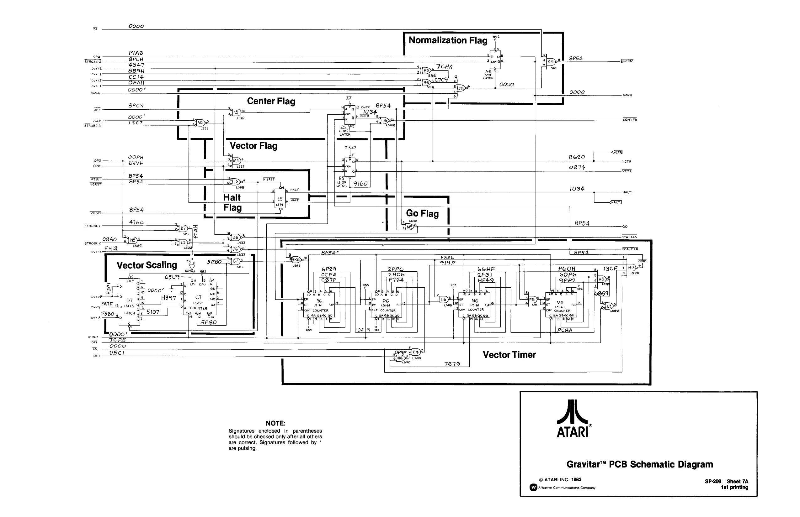
Sheet 7A Normalization Flag Vector Scaling Center Flag Go Flag Vector Flag Vector Timer Halt Flag
Guide to Gravitar PCB Schematics
© ATARI INC., 1982 SP-206 Sheet 3A a viere: commumcarons Comoany 1st printing
This page is a drawing, shown as the original scan.
This page is a drawing, shown as the original scan.
This page is a drawing, shown as the original scan.
This page is a drawing, shown as the original scan.
This page is a drawing, shown as the original scan.
This page is a drawing, shown as the original scan.
This page is a drawing, shown as the original scan.
This page is a drawing, shown as the original scan.
This page is a drawing, shown as the original scan.
This page is a drawing, shown as the original scan.
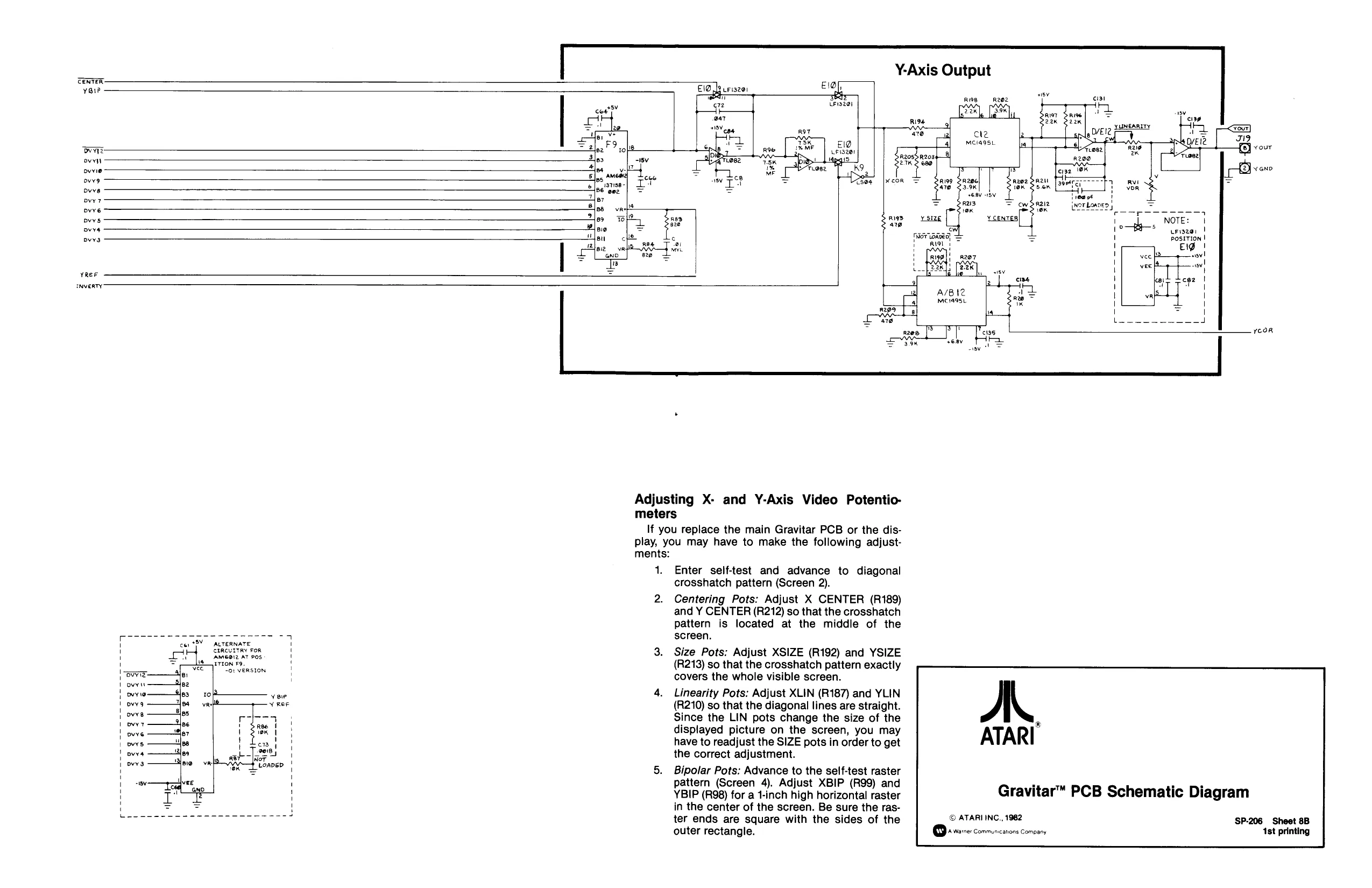
Y-Axis Output
ENTER: 1? ye Rive R202
aaa Ride =, wal cle am 4] MciagS. De owt owe ows. owe bv? ovve pvys pvy4 pvys fe fos fo [a fo fon fa few [rs
z
- + oes ' crises POSITION |
yREE INVERTY
yeoR
Adjusting X- and Y-Axis Video Potentiometers If you replace the main Gravitar PCB or the display, you may have to make the following adjustments:
- Enter self-test and advance to diagonal crosshatch pattern (Screen 2).
- Centering Pots: Adjust X CENTER (R189) and Y CENTER (R212) so that the crosshatch pattern is located at the middle of the peeceeen--- srocccsocct “4 screen.
4 Giecltt ron ' 3. Size Pots: Adjust XSIZE (R192) and YSIZE
= tie tron Fs ‘ (R213) so that the crosshatch pattern exactly aa vee, 01 VERSION owvig———4} covers the whole visible screen.
- Linearity Pots: Adjust XLIN (R187) and YLIN (R210) so that the diagonal lines are straight. Since the LIN pots change the size of the a
displayed picture on the screen, you may ATARI
have to readjust the SIZE pots in order to get the correct adjustment.
- Bipolar Pots: Advance to the self-test raster pattern (Screen 4). Adjust XBIP (R99) and .
YBIP (R98) for a 1-inch high horizontal raster Gravitar™ PCB Schematic Diagram ter ends are square with the sides of the © ATARI INC., 1962 ‘SP-206 Sheet 8B
in the center of the screen. Be sure the ras-
outer rectangle. QA wiarres Communcations Company 1st printing
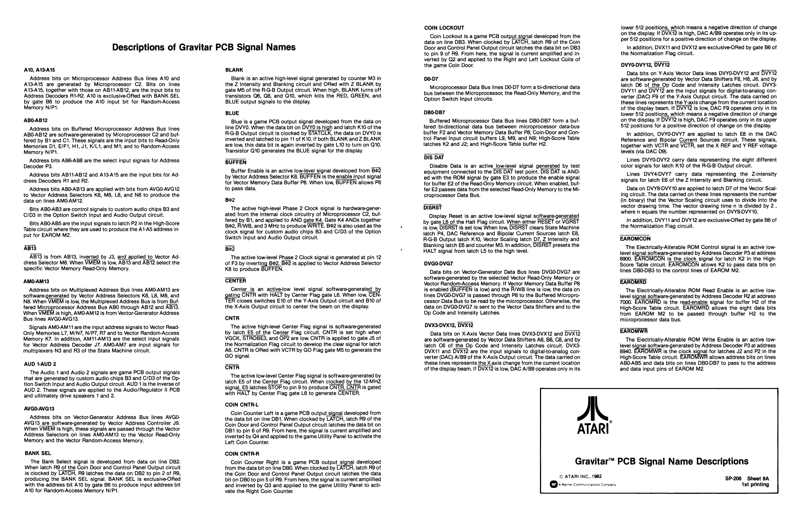
Descriptions of Gravitar PCB Signal Names
A10, A13-A15. Address bits on Microprocessor Address Bus lines A10 and A13-A15 are generated by Microprocessor C2. Bits on lines A13-A15, together with those on AB11-AB12, are the input bits to Address Decoders R1-R2. A10 is exclusive-ORed with BANK SEL by gate B6 to produce the A10 input bit for Random-Access Memory N/P1.
ABO-AB12 Address bits on Buffered Microprocessor Address Bus lines ABO-AB12 are software-generated by Microprocessor C2 and buffered by B1 and C1. These signals are the input bits to Read-Only Memories D1, E/F1, H1, J1, K/L1, and M1; and to Random-Access Memory N/P1. Address bits AB6-AB8 are the select input signals for Address Decoder P3. Address bits AB11-AB12 and A13-A15 are the input bits for Address Decoders R1 and R2. Address bits ABO-AB13 are applied with bits from AVGO-AVG12 to Vector Address Selectors K8, M8, L8, and N8 to produce the data on lines AMO-AM12. Bits ABO-AB3 are control signals to custom audio chips B3 and C/D3 in the Option Switch Input and Audio Output circuit. Bits ABO-AB5 are the input signals to latch P2 in the High-Score Table circuit where they are used to produce the A1-A5 address input for EAROM M2.
ABI3 AB13 is from AB13, inverted by J3, and applied to Vector Address Selector M8. When VMEM is low, AB13 and AB12 select the specific Vector Memory Read-Only Memory.
AMO-AM13, Address bits on Multiplexed Address Bus lines AMO-AM13 are software-generated by Vector Address Selectors K8, L8, M8, and N8. When VMEM is low, the Multiplexed Address Bus is from Buffered Microprocessor Address Bus ABO through AB12 and AB13. When VI is high, AMO-AM12 is from Vector-Generator Address Bus lines AVGO-AVG13. Signals AMO-AM11 are the input address signals to Vector Read- ‘Only Memories L7, M/N7, N/P7, R7 and to Vector Random-Access Memory K7. In addition, AM11-AM13 are the select input signals for Vector Address Decoder J7. AMO-AM7 are input signals for multiplexers N3 and R3 of the State Machine circuit.
AUD 1-AUD 2 The Audio 1 and Audio 2 signals are game PCB output signals that are generated by custom audio chips B3 and C/D3 of the Option Switch Input and Audio Output circuit. AUD 1 is the inverse of AUD 2. These signals are applied to the Audio/Regulator Il PCB and ultimately drive speakers 1 and 2.
AVGO-AVG13 Address bits on Vector-Generator Address Bus lines AVGO- AVG13 are software-generated by Vector Address Controller J9. When VMEM is high, these signals are passed through the Vector Address Selectors on lines AMO-AM13 to the Vector Read-Only Memory and the Vector Random-Access Memory.
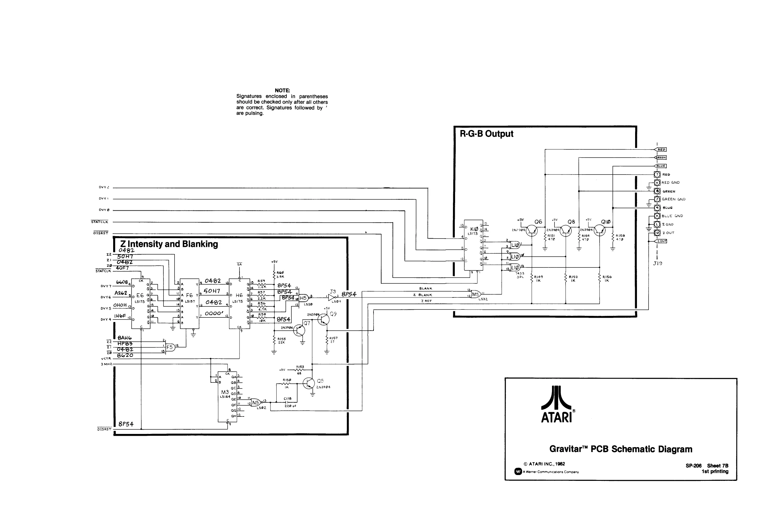
BANK SEL The Bank Select signal is developed from data on line DB2. When latch R9 of the Coin Door and Control Panel Output circuit is clocked by LATCH, R9 latches the data on DB2 to pin 2 of R9, producing the BANK SEL signal. BANK SEL is exclusive-ORed with the address bit A10 by gate B6 to produce input address bit A10 for Random-Access Memory N/P1. BLANK Blank is an active high-level signal generated by counter M3 in the Z Intensity and Blanking circuit and ORed with Z BLANK by gate M5 of the R-G-B Output circuit. When high, BLANK turns off transistors Q6, Q8, and Q10, which kills the RED, GREEN, and BLUE output signals to the display.
BLUE Blue is a game PCB output signal developed from the data on line DVYO. When the data bit on DVY0 is high and latch K10 of the R-G-B Output circuit is clocked by STATCLK, the data on DVYO is inverted and latched to pin 11 of K10. If both BLANK and Z BLANK are low, this data bit is again inverted by gate L10 to turn on Q10. Transistor Q10 generates the BLUE signal for the display.
BUFFEN Buffer Enable is an active low-level signal developed from BO2 by Vector Address Selector K8. BUFFEN is the enable input signal for Vector Memory Data Buffer P8. When low, BUFFEN allows P8 to pass data.
Bo2 The active high-level Phase 2 Clock signal is hardware-generated from the internal clock circuitry of Microprocessor C2, buffered by B1, and applied to AND gate K4. Gate K4 ANDs together Bo2, R/WB, and 3 MHz to produce WRITE. B42 is also used as the clock signal for custom audio chips B3 and C/D3 of the Option Switch Input and Audio Output circuit.
Bo2 The active low-level Phase 2 Clock signal is generated at pin 12 of F3 by inverting BO2. Bé2 is applied to Vector Address Selector K8 to produce BUFFEN.
CENTER Center_is an active-low level signal software-generated_b) gating CNTR with HALT by Center Flag gate L6. When low, CEN. TER closes switches E10 of the Y-Axis Output circuit and B10 of the X-Axis Output circuit to center the beam on the display.
CNTR The active high-level Center Flag signal is software-generated by latch E5 of the Center Flag circuit. CNTR is set high when VGCK, STROBES, and OP2 are low CNTR is applied to gate J5 of the Normalization Flag circuit to develop the clear signal for latch A6. CNTR is ORed with VCTR by GO Flag gate M5 to generate the GO signal.
CNTR The active low-level Center Flag signal is software-generated by latch E5 of the Center Flag circuit. When clocked by the 12-MHZ signal, E5 latches STOP to pin 9 to produce CNTR. CNTR is gated with HALT by Center Flag gate L6 to generate CENTER.
COIN CNTR-L Coin Counter Left is a game PCB output signal developed from the data bit on line DB1, When clocked by LATCH, latch R9 of the Coin Door and Control Panel Output circuit latches the data bit on DB1 to pin 6 of R9. From here, the signal is current amplified and inverted by Q4 and applied to the game Utility Panel to activate the Left Coin Counter.
COIN CNTR-R Coin Counter Right is a game PCB output_signal developed from the data bit on line DBO. When clocked by LAI |, latch R9 of the Coin Door and Control Panel Output circuit latches the data bit on DBO to pin 5 of R9. From here, the signal is current amplified and inverted by Q3 and applied to the game Utility Panel to activate the Right Coin Counter. COIN LOCKOUT Coin Lockout is a game PCB output signal developed from the data on line DB3. When clocked by LATCH, latch R9 of the Coin Door and Control Panel Output circuit latches the data bit on DB3. to pin 9 of R9. From here, the signal is current amplified and inverted by Q2 and applied to the Right and Left Lockout Coils of the game Coin Door.
D0-D7 Microprocessor Data Bus lines DO-D7 form a bi-directional data bus between the Microprocessor, the Read-Only Memory, and the Option Switch Input circuits.
DBO-DB7 Buffered Microprocessor Data Bus lines DBO-DB7 form a buffered bi-directional data bus between microprocessor data-bus buffer F2 and Vector Memory Data Buffer P8; Coin-Door and Control Panel Input circuit buffers L9, M9, and N9; High-Score Table latches K2 and J2; and High-Score Table buffer H2.
DIS DAT Disable Data is an active_low-level signal generated by test equipment connected to the DIS DAT test point. DIS DAT is ANDed with the ROM signal by gate E3 to produce the enable signal for buffer E2 of the Read-Only Memory circuit. When enabled, buffer E2 passes data from the selected Read-Only Memory to the Microprocessor Data Bus.
DISRST Display Reset is an active low-level signal software-generated by gate L6 of the Halt Flag circuit. When either RESET or VGRST is low, DISRST i8 set low When low, DISRST clears State Machine latch P4, DAC Reference and Bipolar Current Sources latch E8, R-G-B Output latch K10, Vector Scaling latch D7, Z Intensity and Blanking latch E6 and counter M3. In addition, DISRST presets the HALT signal from latch L5 to the high level.
DVGO-DVG7 Data bits on Vector-Generator Data Bus lines DVGO-DVG7 are software-generated by the selected Vector Read-Only Memory or Vector Random-Access Memory. If Vector Memory Data Buffer P8 is enabled (BUFFEN is iow) and the R/WB line is low, the data on lines DVGO-DVG7 is passed through P8 to the Buffered Microprocessor Data Bus to be read by the microprocessor. Otherwise, the data on DVGO-DVG7 is sent to the Vector Data Shifters and to the Op Code and Intensity Latches.
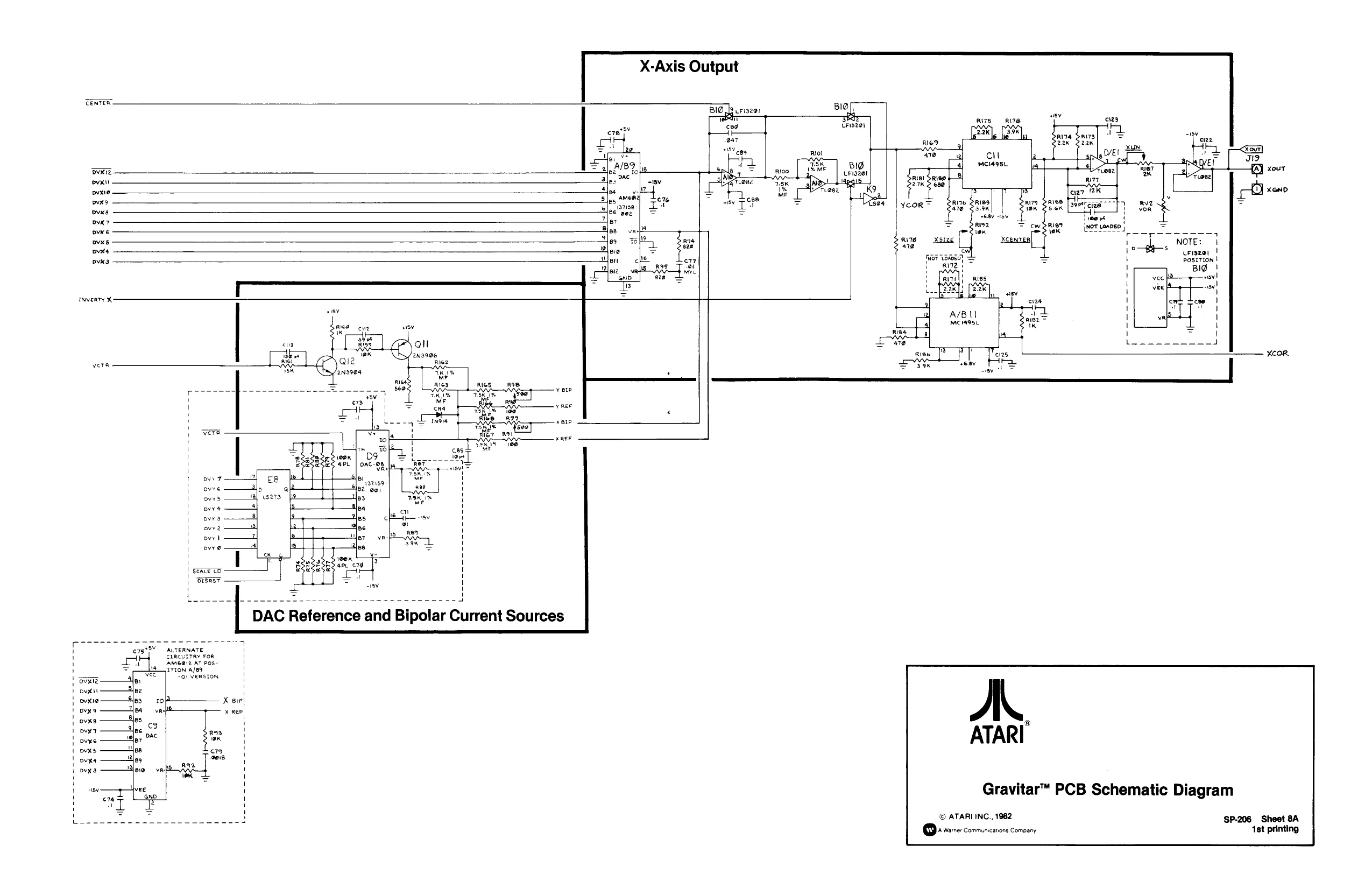
DVX3-DVX12, DVX12 Data bits on X-Axis Vector Data lines DVX3-DVX12 and DVX12 are software-generated by Vector Data Shifters A8, B8, C8, and by latch C6 of the Op Code and Intensity Latches circuit. DVX3- DVX11 and DVX12 are the input signals to digital-to-analog converter (DAC) A/B9 of the X-Axis Output circuit. The data carried on these lines represents the X-axis change from the current location of the display beam. If DVX12 is tow, DAC A/B9 operates only in its
A. ®
ATARI
lower 512 positions, which means a negative direction of change on the display. If DVX12 is high, DAC A/B9 operates only in its upper 512 positions for a positive direction of change on the display. In addition, DVX11 and DVX12 are exclusive-ORed by gate B6 of the Normalization Flag circuit.
DVYO-DVY12, DVY12 Data bits on Y-Axis Vector Data lines DVYO-DVY12 and DVY12 are software-generated by Vector Data Shifters F8, H8, J8, and by latch D6 of the Op Code and Intensity Latches circuit. DVY3- DVY11 and DVY12 are the input signals for digital-to-analog converter (DAC) F9 of the Y-Axis Output circuit. The data carried on these lines represents the Y-axis change from the current location of the display beam. If DVY12 is low, DAC F9 operates only in its lower 512 positions, which means a negative direction of change on the display. If DVY12 is high, DAC F9 operates only in its upper 512 positions for a positive direction of change on the display. In addition, DVYO-DVY7 are applied to latch E8 in the DAC Reference and Bipolar Current Sources circuit. These signals, together with VCTR and VCTR, set the X REF and Y REF voltage levels (via DAC D9). Lines DVYO-DVY2 carry data representing the eight different color signals for latch K10 of the R-G-B Output circuit. Lines DVY4-DVY7 carry data representing the Z-intensity signals for latch E6 of the Z Intensity and Blanking circt Data on DVY8-DVY10 are applied to latch D7 of the Vector Scaling circuit. The data carried on these lines represents the number (in binary) that the Vector Scaling circuit uses to divide into the vector drawing time. The vector drawing time n is divided by 2 , where n equals the number represented on DVY8-DVY10. In addition, DVY11 and DVY12 are exclusive-ORed by gate B6 of the Normalization Flag circuit.
EAROMCON The Electrically-Alterable ROM Control signal is an active lowlevel signal software-generated by Address Decoder P3 at address 8900. EAROMCON is the clock signal for latch K2 in the High- Score Table circuit. EAROMCON allows K2 to pass data bits on lines DBO-DB3 to the control lines of EAROM M2.
EAROMRD The Electrically-Alterable ROM Read Enable is an active lowlevel signal software-generated by Address Decoder R2 at address. 7000. EAROMRD is the read-enable signal for buffer H2 of the High-Score Table circuit. EAROMRD allows the eight data bits from EAROM M2 to be passed through buffer H2 to the microprocessor data bus.
EAROMWR The Electrically-Alterable ROM Write Enable is an active lowlevel signet software-generated by Address Decoder P3 at address.
8940. is the clock Signal for latches J2 and P2 in the
High-Score Table circuit. allows address bits on lines ABO-AB5 and data bits on lines DBO-DB7 to pass to the address and data input pins of EAROM M2.
Gravitar™ PCB Signal Name Descriptions
© ATARI INC., 1982 ‘SP-206 Sheet 9A
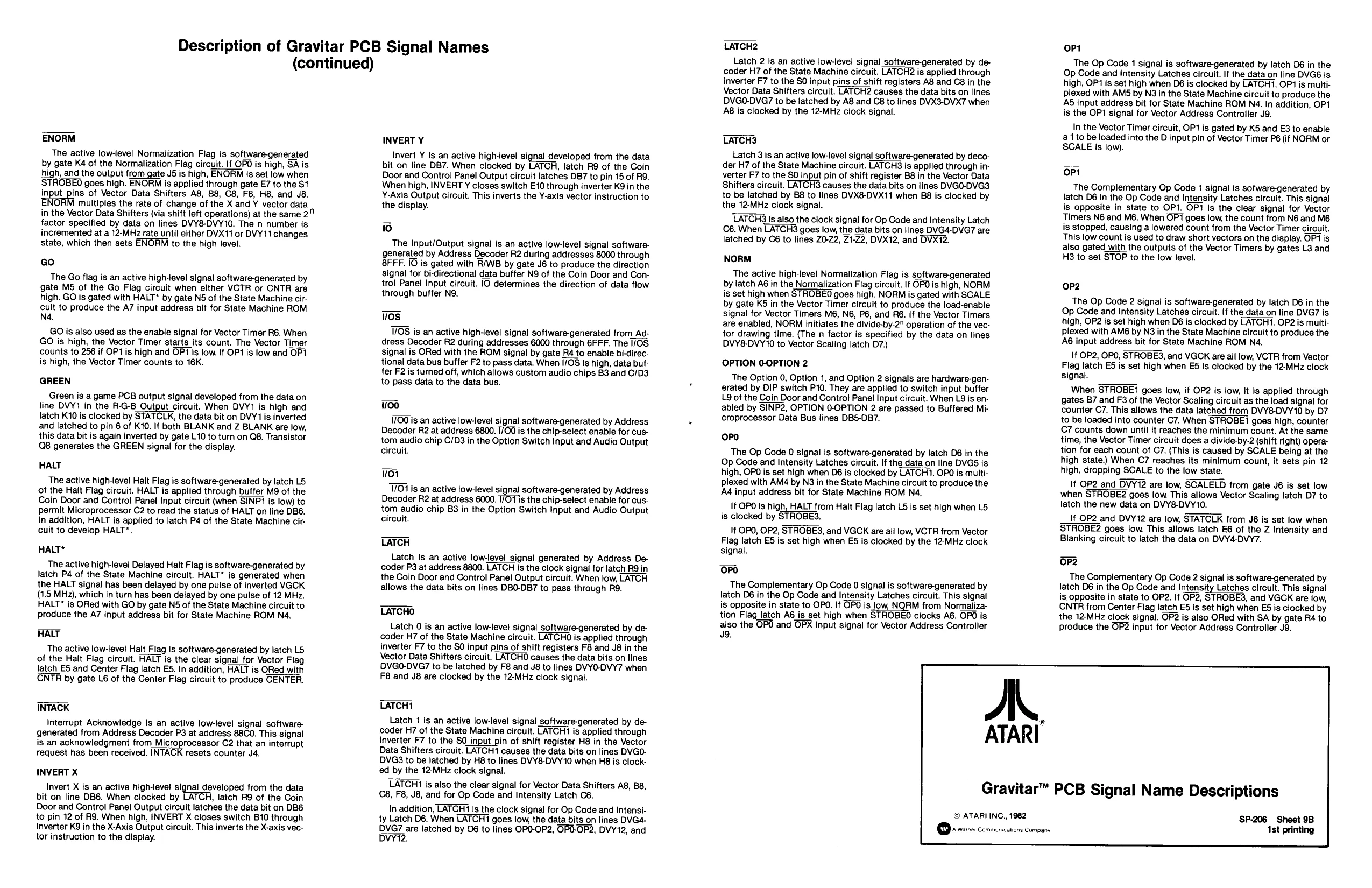
Description of Gravitar PCB Signal Names
(continued)
ENORM The active low-level Normalization Fiag is software-generated by gate K4 of the Normalization Flag circuit. If OPO is high, SA is high, and the output from gate J5 is high, ENORM is set low when STROBEO goes high. ENORM is applied through gate E7 to the S1 input_pins of Vector Data Shifters A8, B8, C8, F8, H8, and J8. ENORM multiples the rate of change of the X and Y vector data in the Vector Data Shifters (via shift left operations) at the same 2 factor specified by data on lines DVY8-DVY10. The n number is incremented at a 12-MHz rate until either DVX11 or DVY11 changes ‘state, which then sets ENORM to the high level.
Go The Go flag is an active high-level signal software-generated by gate M5 of the Go Flag circuit when either VCTR or CNTR are high. GO is gated with HALT* by gate N5 of the State Machine circuit to produce the A7 input address bit for State Machine ROM N4. GO is also used as the enable signal for Vector Timer R6. When GO is high, the Vector Timer starts its count. The Vector Timer counts to 256 if OP1 is high and OP1 is low. If OP1 is low and OP1 is high, the Vector Timer counts to 16K.
GREEN Green is a game PCB output signal developed from the data on line DVY1 in the R-G-B Output circuit. When DVY1 is high and latch K10 is clocked by STATCLK, the data bit on DVY1 is inverted and latched to pin 6 of K10. If both BLANK and Z BLANK are low, this data bit is again inverted by gate L10 to turn on Q8. Transistor Q8 generates the GREEN signal for the display.
HALT The active high-level Halt Flag is software-generated by latch L5 of the Halt Flag circuit. HALT is applied through buffer M9 of the Coin Door and Control Panel Input circuit (when SINP1 is low) to Permit Microprocessor C2 to read the status of HALT on line DB6. In addition, HALT is applied to latch P4 of the State Machine circuit to develop HALT*.
HALT* The active high-level Delayed Halt Flag is software-generated by latch P4 of the State Machine circuit. HALT* is generated when the HALT signal has been delayed by one pulse of inverted VGCK (1.5 MH2), which in turn has been delayed by one pulse of 12 MHz. HALT* is ORed with GO by gate NS of the State Machine circuit to Produce the A7 input address bit for State Machine ROM N4.
HALT The active low-level Halt Flag is software-generated by latch L5
of the Halt Flag circuit. HALT is the clear signal for Vector Flag
latch ES and Center Flag latch E5. In addition, HALT is ORed with CNTR by gate L6 of the Center Flag circuit to produce CENTER.
INTACK Interrupt Acknowledge is an active low-level signal softwaregenerated from Address Decoder P3 at address 88C0. This signal is an acknowledgment from Microprocessor C2 that an interrupt request has been received. INTACK resets counter J4.
INVERT X Invert X is an active high-level signal developed from the data bit on line DB6. When clocked by LATCH, latch R9 of the Coin Door and Control Panel Output circuit latches the data bit on DB6 to pin 12 of R9. When high, INVERT X closes switch B10 through inverter K9 in the X-Axis Output circuit. This inverts the X-axis vector instruction to the display. INVERT Y Invert Y is an active high-level signal developed from the data bit on line DB7. When clocked by LATCH, latch R9 of the Coin Door and Control Panel Output circuit latches DB7 to pin 15 of R9. When high, INVERT Y closes switch E10 through inverter K9 in the Y-Axis Output circuit. This inverts the Y-axis vector instruction to the display.
The Input/Output signal is an active low-level signal softwaregenerated by Address Decoder R2 during addresses 8000 through 8FFF. IO is gated with R/WB by gate J6 to produce the direction signal for bi-directional data buffer N9 of the Coin Door and Control Panel Input circuit. [0 determines the direction of data tlow through buffer N9.
vos W/OS is an active high-level signal software-generated from Address Decoder R2 during addresses 6000 through 6FFF. The /OS. signal is ORed with the ROM signal by gate R4 to enable bi-directional data bus buffer F2 to pass data. When I/OS is high, data buffer F2 is turned off, which allows custom audio chips B3 and C/D3 to pass data to the data bus.
1100 1/00 is an active low-level signal software-generated by Address Decoder R2 at address 6800. I/O0 is the chip-select enable for custom audio chip C/D3 in the Option Switch Input and Audio Output circuit.
1/01 is an active low-level signal software-generated by Address Decoder R2 at address 6000. T/OTis the chip-select enable for custom audio chip B3 in the Option Switch Input and Audio Output circuit,
LATCH Latch is an active low-level signal generated by Address Decoder P3 at address 8800. LATCH is the clock signal for latch R9 in the Coin Door and Control Panel Output circuit. When low, LATCH allows the data bits on lines DBO-DB7 to pass through R9.
LATCHO Latch 0 is an active low-level signal_software-generated by decoder H7 of the State Machine circuit. LATCHO is applied through inverter F7 to the SO input pins of shift registers F8 and J8 in the Vector Data Shifters circuit. LATCHO causes the data bits on lines DVG0-DVG7 to be latched by F8 and J8 to lines DVYO-DVY7 when F8 and J8 are clocked by the 12-MHz clock signal.
LATCH1 Latch 1 is an active low-level signal_software-generated by decoder H7 of the State Machine circuit. LATCH1 is applied through inverter F7 to the SO_input pin of shift register H8 in the Vector Data Shifters circuit. LATCH1 causes the data bits on lines DVGO- DVG3 to be latched by H8 to lines DVY8-DVY10 when H8 is clocked by the 12-MHz clock signal. LATCH is also the clear signal for Vector Data Shifters A8, B8, C8, F8, J8, and for Op Code and Intensity Latch C6. In addition, LATCH1 is the clock signal for Op Code and Intensity Latch D6. When LATCH goes low, the data bits on lines DVG4- DVG7 are latched by D6 to lines OPO-OP2, OPO-OP2, DVY12, and LATCH2 Latch 2 is an active low-level signal software-generated by decoder H7 of the State Machine circuit. LATCH2 is applied through inverter F7 to the SO input pins of shift registers A8 and C8 in the Vector Data Shifters circuit. LATCH2 causes the data bits on lines DVGO-DVG7 to be latched by A8 and C8 to lines DVX3-DVX7 when A8 is clocked by the 12-MHz clock signal.
LATCH3 Latch 3 is an active low-level signal software-generated by decoder H7 of the State Machine circuit. LATCH3 is applied through inverter F7 to the SO input pin of shift register B8 in the Vector Data
Shifters circuit. LAI CHS causes the data bits on lines DVGO-DVG3
to be latched by B8 to lines DVX8-DVX11 when B8 is clocked by the 12-MHz clock signal. LATCH is also the clock signal for Op Code and Intensity Latch C6. When LATCHS goes low, the data bits on lines DVG4-DVG7 are latched by C6 to lines Z0-22, 21-22, DVX12, and DVX12.
NORM The active high-level Normalization Flag is software-generated by latch A6 in the Normalization Flag circuit. |f OPO is high, NORM is set high when STROBEO goes high. NORM is gated with SCALE by gate K6 in the Vector Timer circuit to produce the load-enable signal for Vector Timers M6, N6, P6, and R6. If the Vector Timers are enabled, NORM initiates the divide-by-2" operation of the vector drawing time. (The n factor is specified by the data on lines DVY8-DVY10 to Vector Scaling latch D7.)
OPTION 0-OPTION 2 The Option 0, Option 1, and Option 2 signals are hardware-generated by DIP switch P10. They are applied to switch input buffer L9 of the Coin Door and Control Panel Input circuit. When L9 is enabled by SINP2, OPTION O-OPTION 2 are passed to Buffered Microprocessor Data Bus lines DB5-DB7.
OPO The Op Code 0 signal is software-generated by latch D6 in the Op Code and Intensity Latches circuit. If the data on line DVGS is high, OPO is set high when D6 is clocked by LATCH1. OP0 is multiplexed with AM4 by N3 in the State Machine circuit to produce the A4 input address bit for State Machine ROM N4. |f OPO is high, HALT from Halt Flag latch L5 is set high when L5 is clocked by STROBES. If OPO, OP2, STROBES, and VGCK are all low, VCTR from Vector Flag latch ES is set high when ES is clocked by the 12-MHz clock signal.
OPO The Complementary Op Code 0 signal is software-generated by latch D6 in the Op Code and Intensity Latches circuit. This signal is opposite in state to OPO. If OPO is low, NORM from Normalization Flag latch A6 is set high when STROBEO clocks A6. OPO is also the OPO and OPX input signal for Vector Address Controller J9.
ATARI
OP1 The Op Code 1 signal is software-generated by latch D6 in the Op Code and Intensity Latches circuit. If the data on line DVG6 is high, OP1 is set high when D6 is clocked by LATCH1. OP1 is multiplexed with AMS by N3 in the State Machine circuit to produce the AS input address bit for State Machine ROM N4. In addition, OP1 is the OP1 signal for Vector Address Controller J9. In the Vector Timer circuit, OP1 is gated by K5 and E3 to enable a1 to be loaded into the D input pin of Vector Timer P6 (if NORM or SCALE is low).
OP1 The Complementary Op Code 1 signal is sofware-generated by latch D6 in the Op Code and Intensity Latches circuit. This signal is opposite in state to OP1. OP1 is the clear signal for Vector Timers N6 and M6. When OP1 goes low, the count from N6 and M6 is stopped, causing a lowered count from the Vector Timer circuit. This low count is used to draw short vectors on the display. OP1 is also gated_with the outputs of the Vector Timers by gates L3 and H3 to set STOP to the low level.
OP2 The Op Code 2 signal is software-generated by latch D6 in the Op Code and Intensity Latches circuit. If the data on line DVG7 is high, OP2 is set high when D6 is clocked by LATCH1. OP2 is muitiplexed with AM6 by N3 in the State Machine circuit to produce the A6 input address bit for State Machine ROM N4. If OP2, OPO, STROBES, and VGCK are all low, VCTR from Vector Flag latch ES is set high when ES is clocked by the 12MHz clock signal. When STROBE1 goes low, if OP2 is low, it is applied through gates B7 and F3 of the Vector Scaling circult as the load signal for counter C7. This allows the data latched from DVY8-DVY10 by D7 to be loaded into counter C7. Wnen STROBE! goes high, counter C7 counts down until it reaches the minimum count. At the same time, the Vector Timer circuit does a divide-by-2 (shift right) operation for each count of C7. (This is caused by SCALE being at the high state.) When C7 reaches its minimum count, it sets pin 12 high, dropping SCALE to the low state. If OP2 and DVY12 are low, SCALELD from gate J6 is set low when STROBE2 goes low This allows Vector Scaling latch D7 to latch the new data on DVY8-DVY10. If OP2 and DVY12 are low, STATCLK from J6 is set low when STROBE2 goes low This allows latch E6 of the Z Intensity and Blanking circuit to latch the data on DVY4-DVY7.
OP2 The Complementary Op Code 2 signal is software-generated by latch D6 in the Op Code and Intensity Latches circuit. This signal is opposite in state to OP2. If OP2, STROBES, and VGCK are low, CNTR from Center Flag latch E5 is set high when E5 is clocked by the 12-MHz clock signal. OP2 is also ORed with SA by gate R4 to produce the OP2 input for Vector Address Controller J9.
Gravitar™ PCB Signal Name Descriptions
© ATARI INC., 1982 SP-206 Sheet 9B
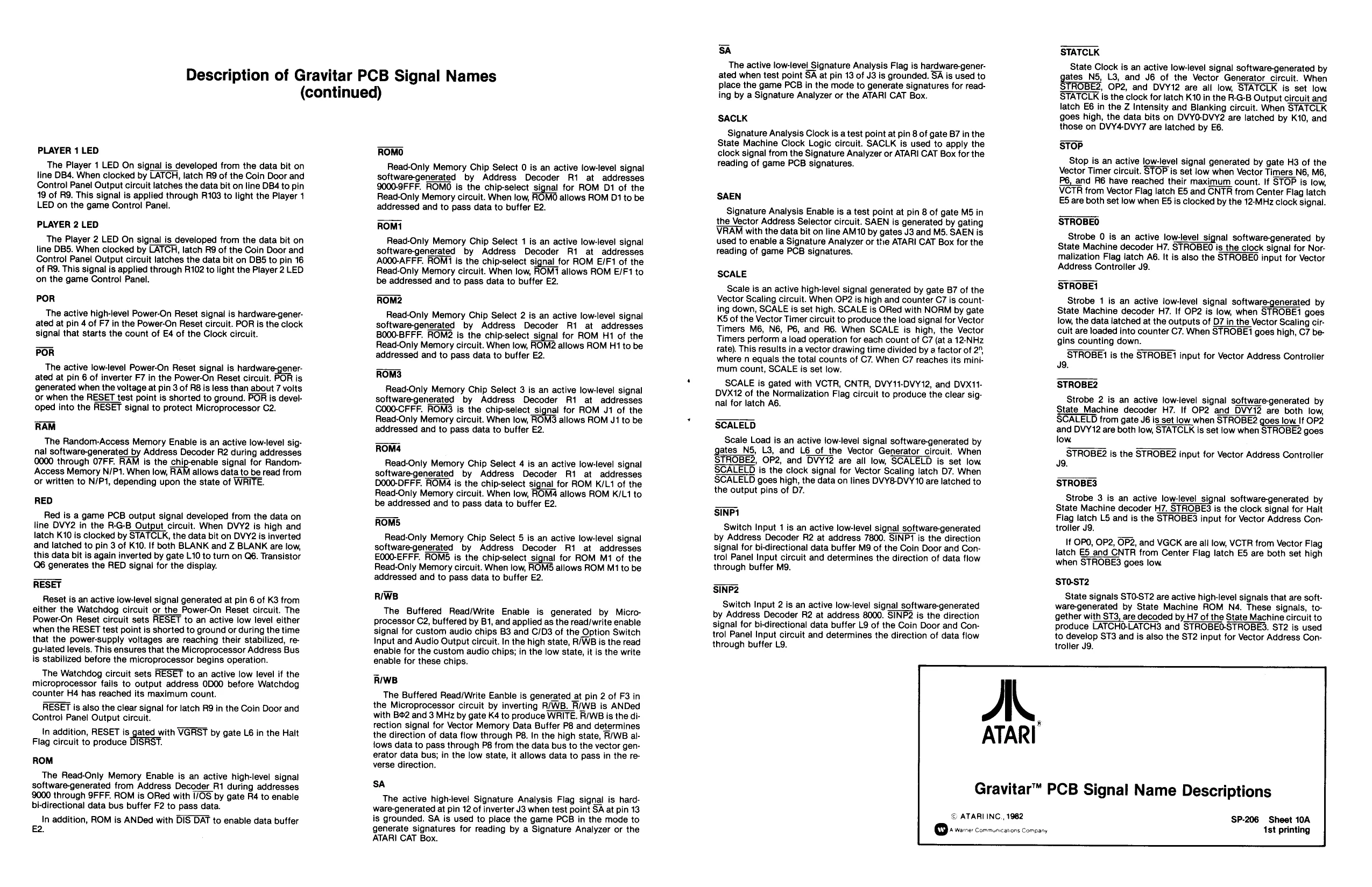
Description of Gravitar PCB Signal Names
(continued)
PLAYER 1LED The Player 1 LED On signal is developed from the data bit on
line DB4, When clocked by LATCH, latch R9 of the Coin Door and
Control Panel Output circuit latches the data bit on line DB4 to pin 19 of R9. This signal is applied through R103 to light the Player 1 LED on the game Control Panel.
PLAYER 2 LED The Player 2 LED On signal is developed from the data bit on line DBS. When clocked by LATCH, latch R9 of the Coin Door and Control Panel Output circuit latches the data bit on DBS5 to pin 16 of R9. This signal is applied through R102 to light the Player 2 LED ‘on the game Controi Panel.
POR The active high-level Power-On Reset signal is hardware-generated at pin 4 of F7 in the Power-On Reset circuit. POR is the clock signal that starts the count of E4 of the Clock circuit.
POR The active low-level Power-On Reset signal is hardware-generated at pin 6 of inverter F7 in the Power-On Reset circuit. POR is generated when the voltage at pin 3 of R8 is less than about 7 volts or when the RESET test point is shorted to ground. POR is developed into the RESET signal to protect Microprocessor C2.
RAM The Random-Access Memory Enable is an active low-level signal software-generated by Address Decoder R2 during addresses 0000 through 07FF. RAM is the chip-enable signal for Random- Access Memory N/P1. When low, RAM allows data to be read from or written to N/P1, depending upon the state of WRITE.
Red is a game PCB output signal developed from the data on line DVY2 in the R-G-B Output circuit. When DVY2 is high and latch K10 is clocked by STATCLK, the data bit on DVY2 is inverted and latched to pin 3 of K10. If both BLANK and Z BLANK are low, this data bit is again inverted by gate L10 to turn on Q6. Transistor Q6 generates the RED signal for the display.
RESET Reset is an active low-level signal generated at pin 6 of K3 from either the Watchdog circuit or the Power-On Reset circuit. The Power-On Reset circuit sets RESET to an active low level either when the RESET test point is shorted to ground or during the time that the power-supply voltages are reaching their stabilized, regu-lated levels. This ensures that the Microprocessor Address Bus is stabilized before the microprocessor begins operation. The Watchdog circuit sets RESET to an active low level if the microprocessor fails to output address 0D00 before Watchdog counter H4 has reached its maximum count. RESET is also the clear signal for latch R9 in the Coin Door and Control Panel Output circuit. In addition, RESET is gated with VGRST by gate L6 in the Halt Flag circuit to produce DI. xT.
ROM The Read-Only Memory Enable is an active high-level signal software-generated from Address Decoder R1 during addresses 9000 through 9FFF. ROM is ORed with I/0S by gate R4 to enable bi-directional data bus buffer F2 to pass data. In addition, ROM is ANDed with DIS DAT to enable data buffer £2. ROMO Read-Only Memory Chip Select 0 is an active low-level signal
| software-generated | by | Address | Decoder | Ri | at | addresses |
9000-9FFF. ROMO is the chip-select signal for ROM D1 of the Read-Only Memory circuit. When low, allows ROM D1 to be addressed and to pass data to buffer E2.
ROM1 Read-Only Memory Chip Select 1 is an active low-level signal
| software-generated | by | Address | Decoder | R1 | at | addresses |
AO00-AFFF. ROM1 is the chip-select signal for ROM E/F1 of the Read-Only Memory circuit. When low, ROM? allows ROM E/F1 to be addressed and to pass data to buffer E2.
ROM2 Read-Only Memory Chip Select 2 is an active low-level signal
| software-generated | by | Address | Decoder | R1 | at | addresses |
B000-BFFF. ROM2 is the chip-select signal for ROM H1 of the Read-Only Memory circuit. When low, ROM2 allows ROM H1 to be addressed and to pass data to buffer E2.
ROM3 Read-Only Memory Chip Select 3 is an active low-level signal
| software-generated | by | Address | Decoder | R1 | at | addresses |
CO00-CFFF. ROMS is the chip-select, sone! for ROM J1 of the
Read-Only Memory circuit. When low, ROMS allows ROM J1 to be addressed and to pass data to buffer E2.
ROM4 Read-Only Memory Chip Select 4 is an active low-level signal
| software-generated | by | Address | Decoder | R1 | at | addresses |
D000-DFFF. ROM4 is the chip-select Signal for ROM K/L1 of the Read-Only Memory circuit. When low, ROM4 allows ROM K/L1 to be addressed and to pass data to buffer E2.
ROM5. Read-Only Memory Chip Select 5 is an active low-level signal
| software-generated | by | Address | Decoder | R1 | at | addresses |
£000-EFFF. ROMS is the chip-select signal for ROM M1 of the Read-Only Memory circuit. When low, ROMS allows ROM M1 to be addressed and to pass data to buffer £2.
RIWB The Buffered Read/Write Enable is generated by Microprocessor C2, buffered by B1, and applied as the read/write enable signal for custom audio chips B3 and C/D3 of the Option Switch Input and Audio Output circuit. In the high state, R/WB is the read enable for the custom audio chips; in the low state, it is the write enable for these chips.
RWB The Buffered Read/Write Eanble is generated at pin 2 of F3 in the Microprocessor circuit by inverting R/WB. RWB is ANDed with B¢2 and 3 MHz by gate K4 to produce WRITE. R/WB is the direction signal for Vector Memory Data Buffer P8 and determines the direction of data flow through P8. In the high state, R/WB allows data to pass through P8 from the data bus to the vector generator data bus; in the low state, it allows data to pass in the reverse direction.
SA The active high-level Signature Analysis Flag signal is hardware-generated at pin 12 of inverter J3 when test point SA at pin 13 is grounded. SA is used to place the game PCB in the mode to generate signatures for reading by a Signature Analyzer or the ATARI CAT Box. SA The active low-level Signature Analysis Flag is hardware-generated when test point SA at pin 13 of J3 is grounded. SA is used to place the game PCB in the mode to generate signatures for reading by a Signature Analyzer or the ATARI CAT Box.
SACLK Signature Analysis Clock is a test point at pin 8 of gate B7 in the State Machine Clock Logic circuit. SACLK is used to apply the clock signal from the Signature Analyzer or ATARI CAT Box for the reading of game PCB signatures.
SAEN Signature Analysis Enable is a test point at pin 8 of gate M5 in the Vector Address Selector circuit. SAEN is generated by gating VRAM with the data bit on line AM10 by gates J3 and M5. SAEN is used to enable a Signature Analyzer or tive ATARI CAT Box for the reading of game PCB signatures.
SCALE Scale is an active high-level signal generated by gate B7 of the Vector Scaling circuit. When OP2 is high and counter C7 is counting down, SCALE is set high. SCALE is ORed with NORM by gate K5 of the Vector Timer circuit to produce the load signal for Vector Timers M6, N6, P6, and R6. When SCALE is high, the Vector Timers perform a load operation for each count of C7 (at a 12-NHz rate). This results in a vector drawing time divided by a factor of 2", where n equals the total counts of C7. When C7 reaches its minimum count, SCALE is set low. SCALE is gated with VCTR, CNTR, DVY11-DVY12, and DVX11- DVX12 of the Normalization Flag circuit to produce the clear signal for latch A6.
SCALELD Scale Load is an active low-level signal software-generated by gates_N5, L3, and L6_of the Vector Generator circuit. When OP2, and DVY12 are ail low, SCALELD is set low SCALELD is the clock signal for Vector Scaling latch D7. When SCALELD goes high, the data on lines DVY8-DVY10 are latched to the output pins of D7.
SINP1 Switch Input 1 is an active low-level signal software-generated by Address Decoder R2 at address 7800. SINPT is the direction signal for bi-directional data buffer M9 of the Coin Door and Control Panel Input circuit and determines the direction of data flow through buffer M9.
SINP2 Switch Input 2 is an active low-level signal software-generated by Address Decoder R2 at address 8000. SINP2 is the direction signal for bi-directional data buffer L9 of the Coin Door and Control Panel Input circuit and determines the direction of data flow through buffer L9.
A
ATARI
STATCLK State Clock is an active low-level signal software-generated by
gies NS, L3, and J6 of the Vector Generator circuit. When
, OP2, and DVY12 are all low, STATCLK is set low STATCLK is the clock for latch K10 in the R-G-B Output circuit and latch E6 in the Z Intensity and Blanking circuit. When STATCLK goes high, the data bits on DVYO-DVY2 are latched by K10, and those on DVY4-DVY7 are latched by E6.
STOP Stop is an active low-level signal generated by gate H3 of the Vector Timer circuit. STOP is set low when Vector Timers N6, M6, P6, and R6 have reached their maximum count. If STOP is low, VCTR from Vector Flag latch E5 and CNTR from Center Flag latch 5 are both set low when ES is clocked by the 12-MHz clock signal.
STROBEO Strobe 0 is an active low-level signal software-generated by State Machine decoder H7. STROBEO is the clock signal for Normalization Flag latch A6. It is also the STROBEO input for Vector Address Controller J9.
STROBE1 Strobe 1 is an active low-level signal software-generated by State Machine decoder H7. If OP2 is low, when STROBE1 goes low, the data latched at the outputs of D7 in the Vector Scaling circuit are loaded into counter C7. When STROBE! goes high, C7 begins counting down. STROBE1 is the STROBE? input for Vector Address Controller Ja,
STROBE2 Strobe 2 is an active low-level signal software-generated by State Machine decoder H7. If OP2 and DVY12 are both low, SCALELD from gate J6 is set low when STROBE2 goes low If OP2 and DVY12 are both low, STATCLK is set low when STROBE2 goes. low STROBE2 is the STROBE2 input for Vector Address Controller J9.
STROBES Strobe 3 is an active low-level_signal software-generated by State Machine decoder H7. STROBES is the clock signal for Halt Flag latch L5 and is the STROBES input for Vector Address Controller J9, If OPO, OP2, OP2, and VGCK are all low, VCTR from Vector Flag latch E5 and CNTR from Center Flag latch E5 are both set high when STROBES goes low
STO-ST2 State signals STO-ST2 are active high-level signals that are software-generated by State Machine ROM N4. These signals, together with ST3, are decoded by H7 of the State Machine circuit to produce LATCHO-LATCH3 and STROBEO-STROBES. ST2 is used to develop ST3 and is also the ST2 input for Vector Address Controller J9.
Gravitar™ PCB Signal Name Descriptions
© ATARI INC. 1982 SP.206 Sheet 10A
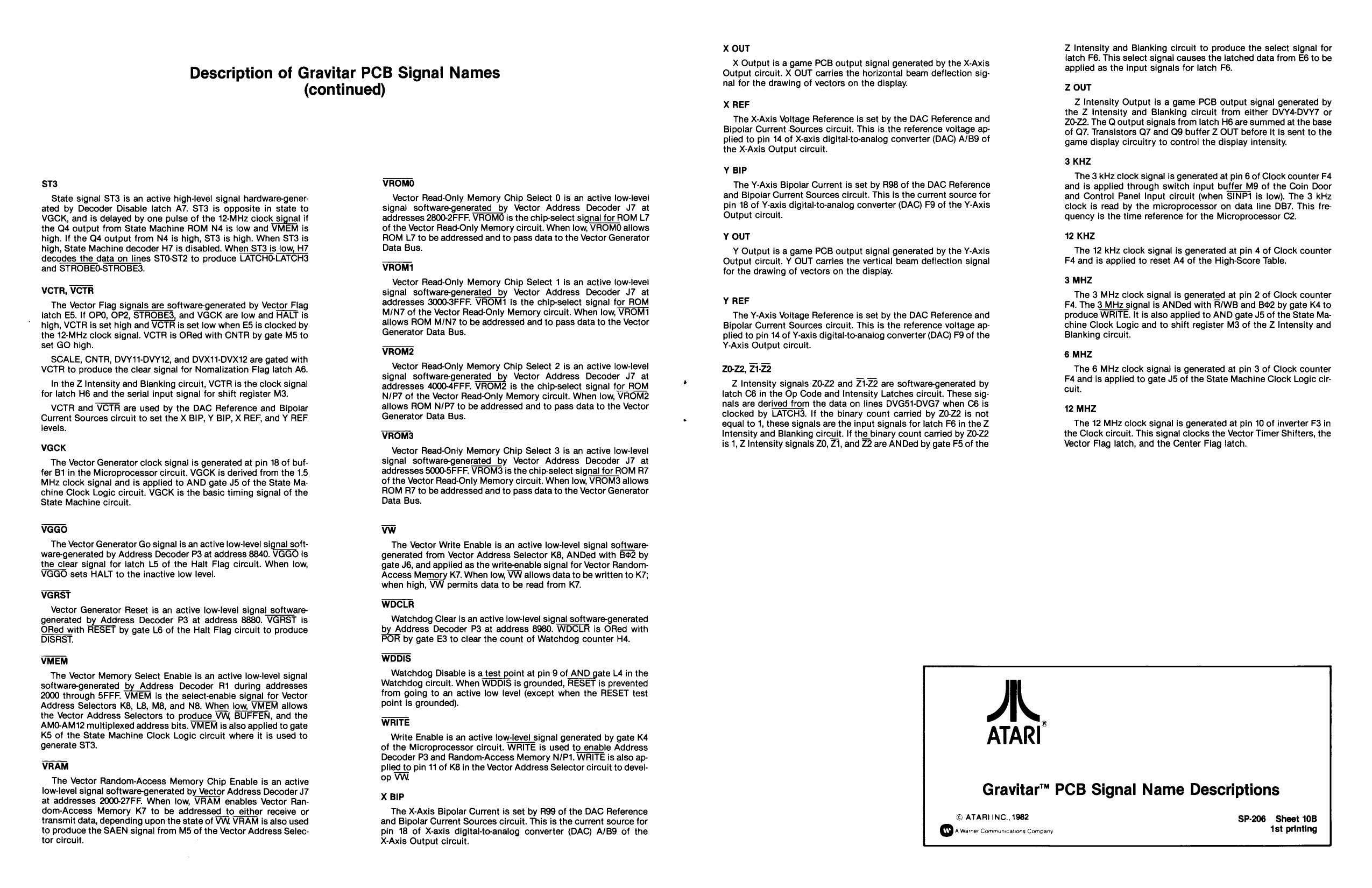
Description of Gravitar PCB Signal Names
(continued)
ST3 State signal ST3 is an active high-level signal hardware-generated by Decoder Disable latch A7. ST3 is opposite in state to VGCK, and is delayed by one pulse of the 12-MHz clock signal if the Q4 output from State Machine ROM N4 is low and VMI is high. If the Q4 output from N4 is high, ST3 is high. When ST3 is high, State Machine decoder H7 is disabled. When ST3 is low, H7 decodes the data on lines STO-ST2 to produce LATCHO-LATCH3 and STROBEO-STROBES.
VCTR, VCTR The Vector Flag signals are software-generated by Vector Flag latch E5. If OPO, OP2, STROBES, and VGCK are low and HALT is high, VCTR is set high and VCTR is set low when E5 is clocked by the 12-MHz clock signal. VCTR is ORed with CNTR by gate M5 to set GO high. SCALE, CNTR, DVY11-DVY12, and DVX11-DVX12 are gated with VCTR to produce the clear signal for Nomalization Flag latch A6. In the Z Intensity and Blanking circuit, VCTR is the clock signal for latch H6 and the serial input signal for shift register M3. VCTR and VCTR are used by the DAC Reference and Bipolar Current Sources circuit to set the X BIP, Y BIP, X REF, and Y REF levels.
VGCK The Vector Generator clock signal is generated at pin 18 of buffer B1 in the Microprocessor circuit. VGCK is derived from the 1.5 MHz clock signal and is applied to AND gate J5 of the State Machine Clock Logic circuit. V@CK is the basic timing signal of the State Machine circuit.
VGGO The Vector Generator Go signal is an active low-level signal software-generated by Address Decoder P3 at address 8840. Vi is the clear signal for latch L5 of the Halt Flag circuit. When low, VGGO sets HALT to the inactive low level.
VGRST Vector Generator Reset is an active low-level signal_softwaregenerated by Address Decoder P3 at address 8880. VGRST is Red with by gate L6 of the Halt Flag circuit to produce DISRST.
VMEM The Vector Memory Select Enable is an active low-level signal software-generated by Address Decoder R1 during addresses 2000 through 5FFF. VMEM is the select-enable signal for Vector Address Selectors K8, L8, M8, and N8. When low, VMEM allows the Vector Address Selectors to produce VW, BUFFEN, and the AMO0-AM12 multiplexed address bits. VMEM is also applied to gate KS of the State Machine Clock Logic circuit where it is used to generate ST3.
VRAM The Vector Random-Access Memory Chip Enable is an active low-level signal software-generated by Vector Address Decoder J7 at addresses 2000-27FF. When low, VRAM enables Vector Random-Access Memory K7 to be addressed _to either receive or transmit data, depending upon the state of VW. VRAM is also used to produce the SAEN signal from M5 of the Vector Address Selector circuit. VROMO Vector Read-Only Memory Chip Select 0 is an active low-level signal software-generated by Vector Address Decoder J7 at addresses 2800-2FFF. VROM0 is the chip-select signal for ROM L7 of the Vector Read-Only Memory circuit. When low, VROMO allows. ROM L7 to be addressed and to pass data to the Vector Generator Data Bus.
VROM1 Vector Read-Only Memory Chip Select 1 is an active low-level signal software-generated by Vector Address Decoder J7 at addresses 3000-3FFF. VROM1 is the chip-select signal for ROM MIN7 of the Vector Read-Only Memory circuit. When low, VROM1 allows ROM MIN7 to be addressed and to pass data to the Vector Generator Data Bus.
VROM2 Vector Read-Only Memory Chip Select 2 is an active low-level signal software-generated by Vector Address Decoder J7 at addresses 4000-4FFF. VRON2 is the chip-select signal for ROM N/P7 of the Vector Read-Only Memory circuit. When low, VROM2 allows ROM N/P7 to be addressed and to pass data to the Vector Generator Data Bus.
VROM3 Vector Read-Only Memory Chip Select 3 is an active low-level signal software-generated by Vector Address Decoder J7 at addresses 5000-5FFF. VROM3 is the chip-select signal for ROM R7 of the Vector Read-Only Memory circuit. When low, VROM3 allows ROM R77 to be addressed and to pass data to the Vector Generator Data Bus.
vw The Vector Write Enable is an active low-level signal softwaregenerated from Vector Address Selector K8, ANDed with B62 by gate J6, and applied as the write-enable signal for Vector Random-
Access Memory K7. When low, VW allows data to be written to K7;
when high, VW permits data to be read from K7.
WDCLR Watchdog Clear is an active low-level signal software-generated
By Address Decoder P3 at address 8980. WDCLR is ORed with
by gate E3 to clear the count of Watchdog counter H4.
WDDIS Watchdog Disable is a test point at pin 9 of AND gate L4 in the Watchdog circuit. When WODIS is grounded, RESET is prevented from going to an active low level (except when the RESET test point is grounded).
WRITE Write Enable is an active low-level signal generated by gate K4 of the Microprocessor circuit. WRITE is used to enable Address Decoder P3 and Random-Access Memory N/P1. WRITE is also applied to pin 11 of K8 in the Vector Address Selector circuit to develop WW.
XBIP The X-Axis Bipolar Current is set by R99 of the DAC Reference and Bipolar Current Sources circuit. This is the current source for pin 18 of X-axis digital-to-analog converter (DAC) A/B9 of the X-Axis Output circuit. X OUT X Output is a game PCB output signal generated by the X-Axis Output circuit. X OUT carries the horizontal beam deflection signal for the drawing of vectors on the display.
X REF The X-Axis Voltage Reference is set by the DAC Reference and Bipolar Current Sources circuit. This is the reference voltage applied to pin 14 of X-axis digital-to-analog converter (DAC) A/B9 of the X-Axis Output circuit.
Y BIP The Y-Axis Bipolar Current is set by R98 of the DAC Reference and Bipolar Current Sources circuit. This is the current source for pin 18 of Y-axis digital-to-analog converter (DAC) F9 of the Y-Axis Output circuit.
Y OUT Y Output is a game PCB output signal generated by the Y-Axis Output circuit. Y OUT carries the vertical beam deflection signal for the drawing of vectors on the display.
Y REF The Y-Axis Voltage Reference is set by the DAC Reference and Bipolar Current Sources circuit. This is the reference voltage applied to pin 14 of Y-axis digital-to-analog converter (DAC) F9 of the Y-Axis Output circuit.
20-22, 21-22 Z Intensity signals Z0-22 and Z1-22 are software-generated by latch C6 in the Op Code and Intensity Latches circuit. These signals are derived from the data on lines DVG51-DVG7 when C6 is clocked by LATCHS. If the binary count carried by Z0-22 is not equal to 1, these signals are the input signals for latch F6 in the Z Intensity and Blanking circuit. If the binary count carried by Z0-Z2 is 1, Z Intensity signals ZO, Z1, and Z2 are ANDed by gate F5 of the
A.
ATARI
Z Intensity and Blanking circuit to produce the select signal for latch F6. This select signal causes the latched data from E6 to be applied as the input signals for latch F6.
Z OUT Z Intensity Output is a game PCB output signal generated by the Z Intensity and Blanking circuit from either DVY4-DVY7 or Z0-Z2, The Q output signals from latch H6 are summed at the base of Q7. Transistors Q7 and Q9 buffer Z OUT before it is sent to the game display circuitry to control the display intensity.
3 KHZ The 3 kHz clock signal is generated at pin 6 of Clock counter F4 and is applied through switch input buffer M9 of the Coin Door and Control Panel Input circuit (when SINP1 is low). The 3 kHz clock is read by the microprocessor on data line DB7. This frequency is the time reference for the Microprocessor C2.
12 KHZ The 12 kHz clock signal is generated at pin 4 of Clock counter F4 and is applied to reset A4 of the High-Score Table.
- MHZ The 3 MHz clock signal is generated at pin 2 of Clock counter F4. The 3 MHz signal is ANDed with R/WB and B2 by gate K4 to produce WRITE. It is also applied to AND gate J5 of the State Machine Clock Logic and to shift register M3 of the Z Intensity and Blanking circuit.
6 MHZ The 6 MHz clock signal is generated at pin 3 of Clock counter F4 and is applied to gate J5 of the State Machine Clock Logic circuit.
12 MHZ The 12 MHz clock signal is generated at pin 10 of inverter F3 in the Clock circuit. This signal clocks the Vector Timer Shifters, the Vector Flag latch, and the Center Flag latch.
Gravitar™ PCB Signal Name Descriptions
© ATARI ING., 1982 |A Warner Communications Company ‘SP-206 Sheet 10B
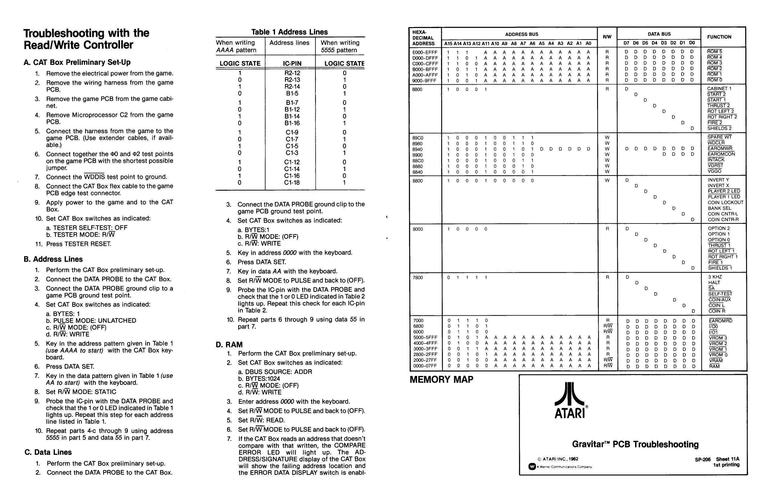
Troubleshooting with the
Read/Write Controller
A. CAT Box Preliminary Set-Up
1. 2.
3.
10.
11. Remove the electrical power from the game. Remove the wiring harness from the game
Remove the game PCB from the game cabinet. Remove Microprocessor C2 from the game PCB. Connect the harness from the game to the game PCB. (Use extender cables, if available.) Connect together the 0 and ©2 test points on the game PCB with the shortest possible jumper. Connect the WDDIS test point to ground. Connect the CAT Box flex cable to the game PCB edge test connector. Apply power to the game and to the CAT Box. Set CAT Box switches as indicated: a. TESTER SELF-TEST: OFF b. TESTER MODE: R/W Press TESTER RESET.
B. Address Lines
1. 2. 3.
10. Perform the CAT Box preliminary set-up. Connect the DATA PROBE to the CAT Box. Connect the DATA PROBE ground clip to a game PCB ground test point. Set CAT Box switches as indicated: a. BYTES: 1 b. PULSE MODE: UNLATCHED c. R/W MODE: (OFF) d. R/W: WRITE Key in the address pattern given in Table 1 (use AAAA to start) with the CAT Box keyboard. Press DATA SET. Key in the data pattern given in Table 1 (use AA to start) with the keyboard. Set R/W MODE: STATIC Probe the IC-pin with the DATA PROBE and check that the 1 or 0 LED indicated in Table 1 lights up. Repeat this step for each address line listed in Table 1. Repeat parts 4-c through 9 using address 55565 in part 5 and data 55 in part 7.
C. Data Lines
1. 2. Perform the CAT Box preliminary set-up. Connect the DATA PROBE to the CAT Box. Table 1 Address Lines When writing Address lines | When writing AAAA pattern 5555 pattern
LOGIC STATE IC-PIN LOGIC STATE
| 1 | R2-12 | 0 |
| 0 | R2-13 | 1 |
| 1 | R2-14 | 0 |
| ie) | B15 | 1 |
| 1 | B17 | 0 |
| 0 | B1-12 | 1 |
| 1 | B1-14 | 0 |
| 0 | B1-16 | 1 |
| 1 | C1-9 | 0 |
| 0 | C1-7 | 1 |
| 1 | C15 | 0 |
| 0 | C13 | 1 |
| 1 | C1-12 | ie) |
| 0 | C1-14 | 1 |
| 1 | C1-16 | 0 |
| 0 | C118 | 1 |
OP MPN
10. Connect the DATA PROBE ground clip to the game PCB ground test point. Set CAT Box switches as indicated:
a. BYTES:1 b. R/W MODE: (OFF) c. R/W: WRITE Key in address 0000 with the keyboard. Press DATA SET. Key in data AA with the keyboard. Set R/W MODE to PULSE and back to (OFF). Probe the IC-pin with the DATA PROBE and
check that the 1 or 0 LED indicated in Table 2
lights up. Repeat this check for each IC-pin in Table 2. Repeat parts 6 through 9 using data 55 in part 7.
D. RAM 1. 2.
NOAA Perform the CAT Box preliminary set-up. Set CAT Box switches as indicated: a. DBUS SOURCE: ADDR b. BYTES:1024 c. R/W MODE: (OFF) d. R/W: WRITE Enter address 0000 with the keyboard. Set R/W MODE to PULSE and back to (OFF). Set R/W: READ. Set R/W MODE to PULSE and back to (OFF). If the CAT Box reads an address that doesn’t compare with that written, the COMPARE ERROR LED will light up. The AD- DRESS/SIGNATURE display of the CAT Box will show the failing address location and the ERROR DATA DISPLAY switch is enabl- HEXA- DECIMAL ADDRESS
E000-EFFF 0000-DFFF C000-CFFF B000-BFFF A000-AFFF 9000-9FFF ADDRESS BUS A15 A14 A13 A12 A11 A10 AQ A8 A7 A6 AS A4 A3 A2 Ai AO DATA BUS
D7 D6 DS D4 D3 D2 Di DO
eloooccce elooccoce
5000-SFFF 4000-4 FF 3000-3FFF 2800-2F FF 2000-27FF 0000-07FF
MEMORY MAP
eloocccceo olooccoce olooccococe olooossaa olosscoss e|scs0404 INVERT Y INVERT X PLAYER 2 LED PLAYER 1 LED COIN LOCKOUT BANK SEL. COIN CNTR-L COIN CNTR-R
OPTION 2 OPTION 1 OPTION 0 THRUST 1 ROT LEFT 1 ROT RIGHT 1 FIRE 1 SHIELDS 1
oo00000000 goo0000000 gvouv00000 oo00000000 goo0000000 go0000000 go0000000 go0000000fo
A.
ATARI
Gravitar™ PCB Troubleshooting
© ATARI INC., 1982 vere conmuncaters Compa SP-206 Sheet 11A
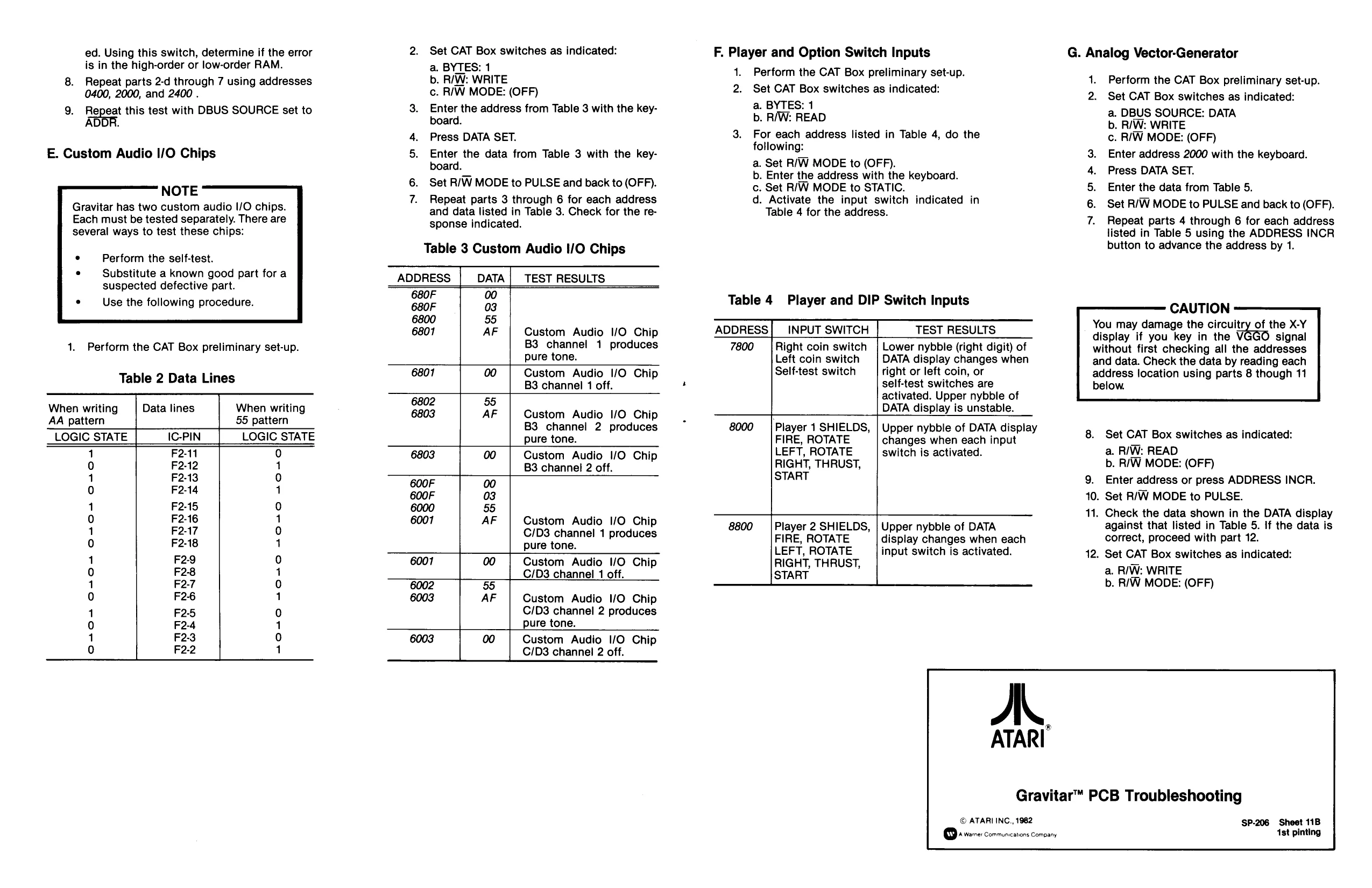
ed. Using this switch, determine if the error is in the high-order or low-order RAM.
- Repeat parts 2-d through 7 using addresses 0400, 2000, and 2400 .
- Repeat this test with DBUS SOURCE set to DOR.
E. Custom Audio I/O Chips
Perform the self-test. Substitute a known good part for a suspected defective part. Use the following procedure.
- Perform the CAT Box preliminary set-up.
Table 2 Data Lines
When writing Data lines When writing AA pattern 55 pattern
LOGIC STATE IC-PIN LOGIC STATE
| 1 | F2-11 | 0 |
| ie) | F2-12 | 1 |
| 1 | F2-13 | 0 |
| 0 | F2-14 | 1 |
| 1 | F2-15 | 0 |
| 0 | F2-16 | 1 |
| 1 | F217 | 0 |
| ie) | F2-18 | 1 |
| 1 | F2-9 | 0 |
| ie) | F2-8 | 1 |
| 1 | F2-7 | 0 |
| (0) | F26 | 1 |
| 1 | F2-5 | 0 |
| 0 | F2-4 | 1 |
| 1 | F2-3 | 0 |
| 0 | F2-2 | 1 |
- Set CAT Box switches as indicated: a. BYTES: 1 b. R/W: WRITE c. RIW MODE: (OFF)
- Enter the address from Table 3 with the keyboard. 4, Press DATA SET.
- Enter the data from Table 3 with the keyboard.
- Set R/W MODE to PULSE and back to (OFF).
- Repeat parts 3 through 6 for each address and data listed in Table 3. Check for the response indicated.
Table 3 Custom Audio I/O Chips
ADDRESS DATA | TEST RESULTS 680F 00 680F 03 6800 55
| 6801 | AF | Custom Audio I/O Chip |
B3 channel 1 produces pure tone.
| 6801 | 00 | Custom Audio I/O Chip |
B3 channel 1 off. 6802 55
| 6803 | AF | Custom Audio I/O Chip |
B3 channel 2 produces pure tone.
| 6803 | 00 | Custom Audio !/O Chip |
B3 channel 2 off. 600F 00 600F 03 6000 55
| 6007 | AF | Custom Audio I/O Chip |
C/D3 channel 1 produces pure tone.
| 6001 | 00 | Custom Audio I/O Chip |
C/D3 channel _1 off. 6002 55
| 6003 | AF | Custom Audio I/O Chip |
C/D3 channel 2 produces pure tone.
| 6003 | 00 | Custom Audio I/O Chip |
C/D3 channel 2 off.
F. Player and Option Switch Inputs
- Perform the CAT Box preliminary set-up.
- Set CAT Box switches as indicated: a. BYTES: 1 b. R/W: READ
- For each address listed in Table 4, do the following: a. Set R/W MODE to (OFF). b. Enter the address with the keyboard. c. Set R/W MODE to STATIC. d. Activate the input switch indicated in Table 4 for the address.
Table 4 Player and DIP Switch Inputs
INPUT SWITCH TEST RESULTS 7800 Right coin switch | Lower nybble (right digit) of Left coin switch DATA display changes when Self-test switch right or left coin, or self-test switches are activated. Upper nybble of DATA display is unstable. 8000 Player 1 SHIELDS, | Upper nybble of DATA display FIRE, ROTATE LEFT, ROTATE RIGHT, THRUST, START changes when each input switch is activated.
Player 2 SHIELDS, FIRE, ROTATE LEFT, ROTATE RIGHT, THRUST, START Upper nybble of DATA display changes when each input switch is activated.
G. Analog Vector-Generator
- Perform the CAT Box preliminary set-up. Set CAT Box switches as indicated: a. DBUS SOURCE: DATA b. R/W: WRITE c. R/W MODE: (OFF) Enter address 2000 with the keyboard. Press DATA SET. Enter the data from Table 5. Set R/W MODE to PULSE and back to (OFF). Repeat parts 4 through 6 for each address listed in Table 5 using the ADDRESS INCR button to advance the address by 1. NOOR w
CAUTION
You may damage the ircultty of the XY
display if you key in the Vi signal without first checking all the addresses and data. Check the data by reading each address location using parts 8 though 11 below.
- Set CAT Box switches as indicated: a. RIW: READ b. RIW MODE: (OFF)
- Enter address or press ADDRESS INCR. 140. Set R/W MODE to PULSE. 11, Check the data shown in the DATA display against that listed in Table 5. If the data is correct, proceed with part 12.
- Set CAT Box switches as indicated: a. RIW: WRITE b. R/W MODE: (OFF)
A
ATARI
Gravitar™ PCB Troubleshooting
© ATARI INC., 1982 SP-206 Sheet 11B Warne: Communications Company ‘1st pinting
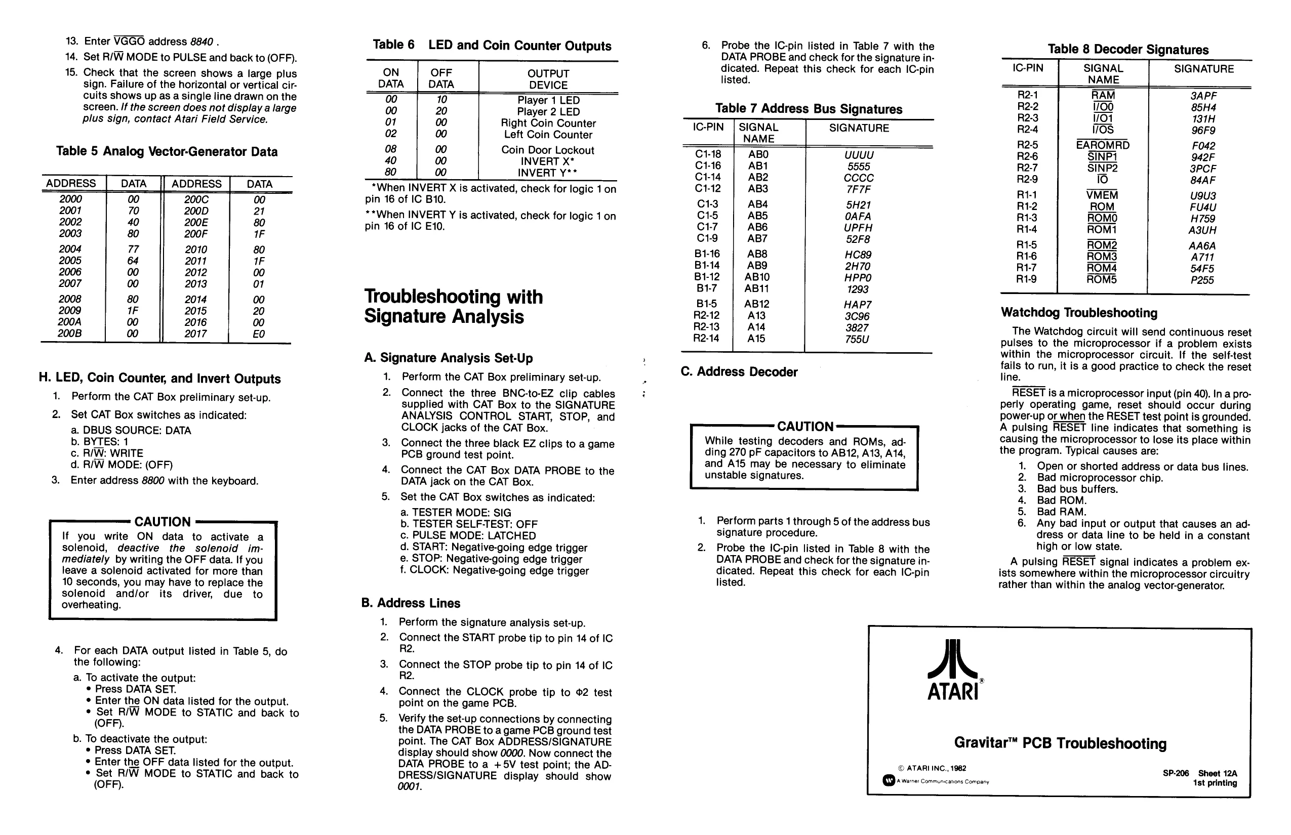
| 13, Enter VGGO address 8840 . | Table 6 | LED and Coin Counter Outputs | 6. | Probe the IC-pin listed in Table 7 with the | Table 8 Decoder Signatures |
DATA PROBE and check for the signature in-
| 14. Set R/W MODE to PULSE and back to (OFF). | dicated. Repeat this check for each IC-pin | IC-PIN | SIGNATURE |
| 15. Check that the screen shows a large plus | OUTPUT | listed. |
sign. Failure of the horizontal or vertical cir- DEVICE R2-1 S3APF
| cuits shows up as a single line drawn on the | Player 1 LED | 5 | |||||
| screen. If the screen does not display a large | Player 2 LED | Table 7 Address Bus Signatures | Fas | 01 | a1 | ||
| plus sign, contact Atari Field Service. | on | Right Coin Counter | IC-PIN | SIGNAL | SIGNATURE | R2-4 | 70S | 96F9 |
02 Left Coin Counter NAME R25 EAROMAD F042
| Table 5 Analog Vector-Generator Data | 08 | Coin Door Lockout | C118 | ABO | UuUU | R2-6 | SINPi | 942F |
| INVERT x’ . | C1-16 | ABI | 5555 | R2-7 | SINP2 | 3PCF | |
| INVERT Y | C1-14 | AB2 | CCCC | R29 | ire) | 84AF | |
| ADDRESS | : | *When INVERT X is activated, check for logic 1 on | C12 | AB3 | 7F7F | R11 | VMEM | ugu3 |
| 00 | pin 16 of IC B10. | c13 | AB4 | 5H21 | R1-2 | ROM. | Fu4au |
70 **When INVERT Y is activated, check for logic 1 on C15 ABS OAFA R13 ROMO H759
| 40 | pin 16 of IC E10. | C17 | AB6 | UPFH | R1-4 | ROM1 | A3UH |
| 80 | C19 | AB7 | 52F8 | R15 | AAGA | ||
| 77 | B1-16 | AB8 | HC89 | R16 | A711 | ||
| 64 | B1-14 | ABS | 2H70 | R1-7 | S4F5 | ||
| 00 | B1-12 | AB10 | HPPO | P255 | |||
| 00 | . | : | B17 | ABI1 | 1293 | ||
| 7 | Troubleshooting with | ets | ABZ | HAP? |
IF Signa ture Analysis R212 AB 3096 Watchdog Troubleshooting
| 00 | R2-13 | Al4 | 3827 | The Watchdog circuit will send continuous reset |
| 00 | R2-14 | AS | 755U | pulses to the microprocessor if a problem exists |
within the microprocessor circuit. If the self-test
| A. Signature Analysis Set-Up | p | ©. Address Decoder | fails to run, it is a good practice to check the reset | |||||
| H. LED, Coin Counter, and Invert Outputs | 1. | Perform the CAT Box preliminary set-up. | : | “RESET | , | ; | in | 40).1 |
| 1 | P | : | 2. Connect the three BNC-to-EZ clip cables | i | R | ls a microprocessor input (pin 40). na pro- | ||
| . | Perform the CAT Box preliminary set-up. | suppli | perly operating game, reset should occur during |
Pplied with CAT Box to the SIGNATURE power-up or when the RESET test point is grounded
| . | i | indi | : | ANALYSIS CONTROL START, STOP, and | - | he | aa | : |
| 2. | Set CAT Box switches as indicated | CLOCK jacks of the CAT Box. | CAUTION | A pulsing RESET line indicates that something is |
a. DBUS SOURCE: DATA causing the microprocessor to lose its place within While testing decoders and ROMs, ad-
| b. BYTES: 1 | 3. Fonnect the nee een EZ clips to a game | ding 270 pF capacitors to AB12, A13, A14, | the program. Typical causes are: | ||
| 6 Rw My ae OF | | ean | eon | and A15 may be necessary to eliminate | 1. Open or shorted address or data bus lines. | |
| . R/W | MODE: | (OFF) | 4. Connect the CAT Box DATA PROBE to the | unstable signatures. | 2. Bad microprocessor chip. |
| 3. | Enter address 8800 with the keyboard. | DATA jack on the CAT Box. | 3. | Bad bus buffers. | |
| 5. Set the CAT Box switches as indicated: | é | ae Fou | |||
| - | . | Ba | |. | ||
| CAUTION | B TESTER Sees OFF | 1. | Perform parts 1 through 5 of the address bus | 6. Any bad input or output that causes an ad- | |
| a | . | c. PULSE MODE: LATCHED | signature procedure. | dress or data line to be held in a constant | |
| sotakee Gamoriie othe ‘solenoid ine | d. START: Negative-going edge trigger | 2. | Probe the IC-pin listed in Table 8 with the | high or low state. | |
| mediately by writing the OFF data. If you | e, STOP: Negative-going edge trigger | DATA PROBE and check for the signature in- | A pulsing RESET signal indicates a problem ex- | ||
| AO seconde: vou ay have to repioce the | ADSI | listed. Post is check for each Ic-pin | rather than within the ansiog vestorgeneratoe |
10 seconds, you may have to replace the solenoid and/or its driver, due to overheating. B. Address Lines
- Perform the signature analysis set-up.
- Connect the START probe tip to pin 14 of IC
| 4. | For each DATA output listed in Table 5, do | R2. |
the following: 3. Connect the STOP probe tip to pin 14 of IC a. To activate the output: R2. 2 ¢ Press DATA SET. 4. Connect the CLOCK probe tip to 62 test ATARI Enter the ON data listed for the output. point on the game PCB.
- Set R/W MODE to STATIC and back to 5. Verify the set-up connections by connecting
| (OFF). | the DATA PROBE to a game PCB ground test | i | . |
| b. To deactivate the output: | point. The CAT Box ADDRESS/SIGNATURE | Gravitar™ | PCB Troubleshooting |
- Press DATA SET. display should show 0000. Now connect the
- Enter the OFF data listed for the output. DATA PROBE to a +5V test point; the AD- © ATARIINC,, 1982 SP-206 Sheet 12A
| ¢ Set R/W MODE to STATIC and back to | DRESS/SIGNATURE display should show | Qa wierrer Communications Company | ‘1st printing |
(OFF). 0001.
This page is a drawing, shown as the original scan.