Centipede DP-182-3rd-02B
Centipede (revision 4) (Atari, 1980) · Drawing Package · 1 pages · original scan
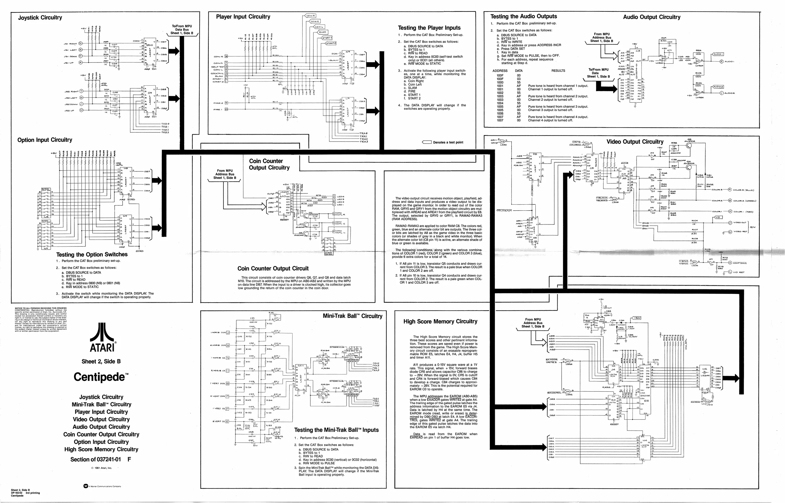
Joystick Circuitry
TolFrom MPU Data Bus Sheet 1, Side 8
Option Input Circuitry
HE
ERED ERE
Testing the Option Switches
Perform the GAT Box preliminary setup.
- Set the CAT Box switches as follows: ‘a. DBUS SOURCE to DATA b. BYTES to1 ©. RIW to READ d. Key in address 0800 (N9) or 0801 (NB) @, RW MODE to STATIC
- Activate the switch while monitoring the DATA DISPLAY. The DATA DISPLAY will change Ifthe switch is operating properly.
Player Input Circuitry
nin aa
rae B =
i
Testing the Player Inputs
- Perform the CAT Box Preliminary Setup.
- Set the CAT Box switches as follows: ‘a. DBUS SOURCE to DATA . BYTES 101 ©. ROW to READ
- Key in address 0000 (self-test switch ‘oniy) oF 0601 fall others). RIW MODE to STATIC
- Activate the following player input switchfs, one at a time, while monitoring the DATA DISPLAY: ‘Coin Right ». Coin Lett . SLAM
- FIRE fe. START
- START2.
- The DATA DISPLAY will change if the ‘switches are operating propery
< Denotes a test point
Testing the Audio Outputs
- Perform the GAT Box preliminary set-up.
2, Sat the CAT Box switches as follows Audio Output Circuitry
- DBUS SOURCE to DATA From MPU b. BYTES tot Address Bus . RAV to WRITE Shoot 4, Side B
- Key in adress or press ADDRESS INCR €. Press DATA SET i Key in data g. Set RAW MODE to PULSE, then to OFF. I. For each address, repeat sequence stating at Stop d ADDRESS DATA RESULTS TolFrom MPU
| 100F | 0 | c. | |
| 100 | 0 | Shoot | 1, Side 8 |
4000 5
| soot | AF | Pure tone is heard from channe! 1 outpu |
| ‘ot | 0) | Channel 1 outputs tuned oft. |
002 3
| 4003. | AF | Pure tone is heard from channel 2output. |
| 1003 | (00 | Channel 2 output is tured oft |
{008 55
| 1005 | AP. | Pure tones near from channel output |
| 108 | (00 | Channel 3 output is tured oft |
+008 5
| 1007 | AP | Pure tones heard from channel 4 output |
| 007 | 0) | Channel ¢ outputs tumed oft |
Coin Counter Output Circuit This circuit consists of coin counter drivers 06, Q7, and Q8 and data latch M10. The circuit is addressed by the MPU on ABO-AB2 and written by the MPU ‘on data line DB7. When the input to a driver is clocked high, its collector goes low grounding the return of the coin counter In the coin door. ‘The video output circuit receives motion object, playfield, address and data Inputs and produces a video output to be displayed on the game monitor. In order to read out of the color AM, GRYO and GRY1 from the motion object circuitry are mut tiplexed with AREAO and AREA from the playfield ciroult by E. The output, selected by GRYO or GRY%, is RAMA-RAMAS (RAM ADDRESS)
RAMAO- RAMAS are applied to color RAM C8. The colors red, ‘green, blue and an alternate colo bit are outputs. The three col Or bits are latched by AB as the game video in the three basic Colors (or shades of gray in a black and white monitor). When the alternate color bit (C8 pin tt) is active, an alternate shade of blue or green is availabe.
‘The following conditions, along with the various combinations of COLOR 1 (eed), COLOR 2 (green) and COLOR 3 (dive), provide 6 extra colors for a total of 14
- 18 pin 1s low, transistor Q5 conducts and draws cur. rent from COLOR 3. The result is apale blue when COLOR, ‘Vand COLOR 2 are off.
- IF AB pin 10is low, transistor Q4 conducts and draws cur- Font from COLOR 2. The result is a pale green when COL- OF 1 and COLOR S are off
A, ATARI
Sheet 2, Side B
Centipede”
Mini-Trak Ball™ Circuitry
Video Output Circuitry Audio Output Circuitry Coin Counter Output Circuitry
High Score Memory Circuitry
Section of 03724101 F
Orme connncnescneny sea, ste @ Seles Se pining Sentnde Mini-Trak Ball™ Circuitry
ct Teo |
sew oj Testing the Mini-Trak Ball™ Inputs
- Perform the CAT Box Preliminary Setup.
- Sat the CAT Box switches as follows: ‘a. DBUS SOURCE to DATA b. BYTES to1 ©. RIW to READ 4d. Key in address 0000 (vertical) or 0602 (horizontal) fe. RW MODE to PULSE ‘3, Spin the MiniTrak Ball™ while monitoring the DATA DIS- PLAY. The DATA DISPLAY will change It the Min-Trak Ball input is operating propery. Ih Score Memory Circuitry
‘The High Score Memory circuit stores the three best scores and other pertinent information. These scores are saved even if power Is. emoved from the game. The High Score Mem Cory circuit consists of an erasable reprogram ‘mable ROM 5, latches E4, H4, J4, buffer HS and timer Att
AAtl_produces a 0-15V square wave at a 1V rate. This signal, when + 15V, forward biases. diode CRS and allows capacitor C86 to charge to ~28V. When the signal is OV, CRS Is cutoff ‘and ORé is forward-biased which causes C84 to develop a charge. C84 charges to approxi: mately ~ 28V. This ts the potential required for EAROM CO to operate.
‘The MPU addresses the EAROM (ABO-AB5) when a low EAADOR gates WRITE2 at gate Ad ‘The trailing edge of the gated pulse latches the ‘address information to the EAROM ES via J Data is latched by Hé at the same time, The EAROM mode (read, write or erase) is deter: ‘mined by DB0-DBS at latch E4. A low EACONates WRITE? at gate Ad. The talling edge of this gated pulse latches the data into the EAROM €5 via latch Ha.
Data_is read from the EAROM when ‘on pin of buffer Hé goes low. Address Bus Sheet 1, Side B