Exterminator
Exterminator (Premier Technology, 1989) · Manual · 47 pages · 19 sections · original scan
GoIHOE,
INSTRUCTION MANUAL
EXTERMINATOR (GAME #V101) © INSTRUCTION MANUAL
TABLE OF CONTENTS
SEC. PAGE lL _ INSTALLATION... we 1+2 We INITIALIZATION. «20200 2 WL = GAME OPERATION........0000.000.000000ccceee 3 IV. SOUND/SPEECH 0.000.002... .00.ccccccceceeteees 3 V. GAMEPLAY AND SCORING... 4-7
VI. GAME ADJUSTMENTS/OPTIONS ................ 8
VI BOOKKEEPING AND SELF TEST ................. 9-11
Vill. GENERAL INFORMATION .........0.......... 12-13
IX THEORY OF OPERATION... 14-24 X. WIRING AND SCHEMATIC DIAGRAMS .......... 25-47 Xl PARTS INFORMATION .....00..0 0 48-49 WELLS GARDNER MONITOR, SERVICE AND OPERATION MANUAL (Attached)
Premier Technology 759 INDUSTRIAL DRIVE BENSENVILLE, IL 60106 1-708-350-0400 TELEX 215009 PRMR FAX: 1-708-350-1097
THE PREMIER HOTLINE 1-800-444-0761
©1989 PREMIER TECHNOLOGY COPYRIGHT ALL RIGHTS RESERVED
“WARNING: This equipment generates, uses, and can radiate radio frequency energy and if not installed and used in accordance with the instructions manual, may cause interference to radio communications. It has been tested and found to comply with the limits for a Class A computing device pursuant to Subpart J of Part 15 of FCC Rules, which are designed to provide reasonable protection against such interference when operated in a commercial environment. Operation of this equipment in a residential area is likely to cause interference in which case the user at his own expense will be required to take whatever measures may be required to correct the interference.”
Premier Technology VIDEO SYSTEM OVERVIEW
The Exterminator video system is a state of the art video graphic system utilizing the latest in video graphics technology to provide color resolution never before seen in a video game!
The heart of the system is two Texas Instruments 34010 Graphics System Processor chips (GSPs) running at 40Mhz. these general purpose micro-processors control the game flow and the video timing.
There are 2 bitmapped video planes, a foreground and a background. The foreground plane has a pixel resolution of 256 X 240 pixels at 8 bits per pixel (or 256 colors). The background plane has the same pixel resolution as the foreground, but with a color resolution of 16 bits per pixel (or 32,768 colors). The foreground plane is strictly color-mapped, while in the background, each pixel has the option of containing its own color map of up to 2048 colors.
Images and program are stored in ROMS with a total potential capacity of 2MB of storage.
One GSP is used as a Master. This GSP controls the game logic as well as the background plane. All ROM is available to the Master GSP, along with 512 KB of scratch RAM. The other GSP functions as a Slave, controlling only the foreground screen. This GSP has 1 MB of RAM available to it. All program and image data is downloaded to the Slave GSP from the Master before the Slave can function.
Backup memory is provided by a EEPROM chip which retains all bookkeeping information along with coin counts and game adjustments when power is shut off. No batteries are needed.
A JAMMA connector supplies all the standard JAMMA signals, while separate ports allow for additional signals to be supplied to the processor. In all, 30 player input lines are available.
A diagnostic connector is supplied to enable a host computer to download diagnostic programs and perform tests on the video board in the field. (This feature will be made available some time in the future).
Il. INSTALLATION
SET-UP
1. Carefully inspect the exterior of the game for any damage which might have occurred during shipment.
Unlock and open the rear cabinet door.
Check that all plug-in connectors are seated firmly. The connectors are keyed so they will only go in one way.
Remove the binding strap from the line cord, and install the line cord plate in the groove provided.
Adjust the (4) attached cabinet levelers as required.
CHECK-UP
1. Check that all cables are free of moving parts.
Check for any loose wires.
Check for loose solder or foreign matter on switches and power supply assemblies.
Be certain all fuses are seated firmly.
Be sure transformer wiring corresponds to the supply voltage.
Refer to section VI to make all the necessary game adjustments.
Reassemble the game.
Plug the line cord into a properly grounded 3-wire receptacle ONLY! ! CONTROL PANEL REMOVAL
Unplug the game.
Unlock and open the coin chute door.
Reach in through the coin chute door and unsnap the (2) latches located on the left and right sides. Grasp the two joysticks and with a concurrent motion of pushing the control panel forward 1/8" and lifting up at the rear of the panel while it pivots on the front edge of the control panel to clear the lockdown bracket. Disconnect cable connectors A9P1/A9J1 and A9P2/A9J2.
Remove the entire control panel assembly from the game.
The joystick and micro | switches now accessible for removal or cleaning.
MONITOR REMOVAL
Unplug the game.
Perform the control panel assembly removal procedure (Section C).
Unlock and open the rear cabinet door.
Lift up the video glass 1/4" to clear the retaining slot and set aside.
Remove the (6) Phillips head screws and carefully remove and set aside the monitor mask.
lL INSTALLATION,
- NOTE: the color monitor contains HIGH VOLTAGES delivering LETHAL quantities of energy. Do not attempt to service the monitor until you have shorted the anode plug on the picture tube to ground.
- Disconnect the two cable connectors A10P4/A10J4 and A12P9/A12J9 mounted on the rear walls of the cabinet.
- Disconnect A3J1 from the monitor PC board and cable connector A12P3/A1233. Remove the ground straps mounted on the monitor frame. Remove the monitor front I. INITIALIZATION
control board mounted on the lower right side.
- Remove the (4) Hex nuts and washers attached to the carriage bolts mounted on each side of the cabinet. Carefully grasp the monitor assembly which includes the wood front mounting and slide it down the wood rails being careful to clear the cables mounted on each side of the cabinet walls
MARQUEE ACCESS
- Remove the (3) button head allen screws to detach the marquee support bracket, remove the screened marquee and set aside.
Il. INITIALIZATION
POWER ON...
The power on process normally takes about 5 seconds. During this time, the screen will show an indeterminate pattern. After a successful initialization, the demo portion of the attract mode will begin.
If there is a problem with the backup memory (EEPROM), then one of 3 things may occur...
- If the EEPROM socket is empty (that is, no EEPROM chip is present) a message will be displayed saying "WARNING! NO EEPROM CHIP IS PRESENT. BOOKKEEPING TOTALS AND GAME ADJUSTMENTS WILL BE LOST WHEN GAME IS POWERED DOWN." The game will function normally, but any information normally stored in EEPROM is initialized 2) to default values. section on EEPROM) (See
If some adjustment parameter is found to be invalid, the message "WARNING! ADJUSTMENTS NEED TO BE RESET. TURN GAME OFF, THEN ON, THEN INFORM SERVICEMAN." will appear. Turning the game off and on should allow the game to start normally, however, should check the game adjustments to make sure they are set the way you want. you
If the EEPROM is found to have invalid data, or if a new EEPROM has just been installed, the message "INITIALIZING EEPROM....PLEASE WAIT" will appear. The initialization will take about 12 seconds and then the demo part of the attract mode will begin.
A. . GAME OPERATION, IV. SOUND/SPEECH
Hl, GAME OPERATION
GAME START
1. Insert coins into coin chute. a. Coin chute sound is played. b. Total credits are displayed on the screen.
Press either start button to start a game. a. Total credits are decreased by one or two depending on the game adjustment setting. b. A demonstration scene is displayed on the screen. This demonstration can be cut short by pressing the start button again. c. The game begins. B. SECOND PLAYER
- A second player may enter the game at any time by pressing the manual start button.
Cc GAME CONTINUATION
Lew A player has ten seconds to continue his game after his bug juice has run dry. Pressing the start button within this time will allow him to proceed with play from his current house and room.
IV. SOUND/SPEECH
ATTRACT MODE
SOUND
Theme music
Typewriter
Assorted sounds
SPEECH
"Help me"
When the Exterminator logo is built on the screen.
When the bug crawls back and forth leaving game instructions.
During the sample play scene in the kitchen.
OCCURRENCE
Speaks every other time the word "Help" appears by a house.
The above attract mode sounds can be turned off by setting the attract sound game adjustment to "No".
GAME MODE
SPEECH
“Ouch" OCCURRENCE
Whenever the hand gets stung, bitten or shot.
GAME PLAY AND SCORING
Bina
In this game, you are a Pest Control Expert sent to a neighborhood to rid it of assorted pests. You are a disembodied hand with a number of skills at your disposal...you can squish enemies by getting them in your palm and closing your hand, you can pound enemies on the ground, and you can shoot enemies by squirting a toxic pesticide out of your finger.
The neighborhood consists of 7 houses, each house having 5 rooms. The combination of rooms is different in each house, and the combinations of enemies are different in each house.
Enemies which cannot harm you are the flies, ants, spiders, gubbers (green bats), nuts, cans, and tomatoes. Enemies which CAN harm you are the wasp, dragonflies, toads, mosquitoes, tanks and squirt bottle. Some enemies appear only on the ground. Others appear only in the air. You can only pound ground enemies, and you can either shoot or squish flying enemies. Table 1 shows the wave structure of the game.
When the game begins, your "JUICE" gauge reads full. Any number of things can rob you of juice. Some things can restore your juice. The game ends when you run out of juice. If you want to continue playing, you can drop in another coin and receive full JUICE again. The only time you cannot immediately continue playing when you run out of juice is during the Ultimate Challenge, which is explained later. Dangerous enemies each have different characteristics and need to be handled differently. All flying enemies can be shot. All ground enemies can be pounded.
WASP - The wasp will seek out your hand and then sting you. If you squish it, you will get stung anyway. Being stung will rob you of some juice. If a wasp is hovering around you, shake your hand (by shaking the joystick) to make it go away. Shooting it will delay another wasp from seeking you. MOSQUITOES - The mosquitoes seek you out and bite you. This also robs you of your juice. Shaking has no effect on them, but you can squish them without harm. DRAGONFLIES - Dragonflies can be squished without harm also, but they randomly drop bombs which zap you (and take away some juice) when they explode. If you grab a bomb BEFORE it explodes you RECEIVE a small amount of juice. TOY TANKS - The tanks fire live ammo. If your hand is hit, you lose some juice. Tanks can be pounded. TOADS - The toads will shoot their tongues out and suck you into their mouths. This will also cause a loss of juice. Toads can also be pounded. SQUIRT BOTTLE - The squirt bottle shoots juice back at you. If you get hit, you lose some juice. It never shoots while it is
V. GAME PLAY AND SCORING
moving, and it only moves when you move towards it. If you CAN grab it, you receive some juice.
In addition to all the enemies, there is a glowing dodecahedron which (if grabbed) will supply you with some extra juice. This dodecahedron is not harmful to you -in any way.
You always have the choice of which skill to use at any given time. To shoot, make sure your hand is all the way over to your side of the screen (Left for the left player, Right for the right player). When this is done, the hand moves into a shooting position (forefinger pointing only). Now when the joystick button is pressed, the hand will fire. Rotating the stick and moving it up and down will allow aiming to every part of the room except directly across to where the other player is.
Moving the hand toward the center of the screen while the button is released causes the hand to open. Now when the joystick button is pressed, the hand will close, squishing anything in its grasp.
The pound button will cause the hand to pound onto the ground. The hand must. be at a certain minimum height for pounding to work. If the hand is too low, a message flashes on saying "TOO LOW TO POUND".
The floor of each room contains 6 lanes of tiles. When you squish, pound of shoot anything in the air (EXCEPT THE SQUIRT BOTTLE) it falls to the ground and changes the color of the tile it lands on. If the left (red) player shot it, the tile turns red. If the right (blue) player shot it, it turns blue. When an entire lane of tiles (from front to back) contains a single color, then that player has completed the room and won that wave. The next room is determined by which lane was completed. (Each lane is labelled with a room name depending on which rooms are left to be completed in that house).
When an enemy falls on a tile directly under your hand, the game will rotate that lane so the next tile which is NOT YOUR COLOR appears underneath your hand in that lane. This is done to make all your pounds and squishes work to your advantage.
BONUS ROUNDS
Some basement and kitchen waves are bonus rounds. Whichever player completes these rooms is entitled to 20 seconds of free gameplay to earn extra points. In the kitchen, the player can pound as many bugs and food items as possible within the 20 seconds. The basement gets turned into a shooting gallery with rats running up and down the shelves.
WARP FEATURE (optional feature)
In the kitchen waves of houses 1 and 3, the freezer door will open momentarily for an instant. If either player is shooting into the open freezer, gameplay will warp to the next house and the player (or players) who made the shot will be awarded 250,000 points.
ULTIMATE WAVE
After seven houses are completed, you find yourself outdoors and faced with an ultimate challenge. You must withstand the attacks of toads, dragonflies, mosquitoes and squirt bottles. In this wave, there are no tiles. Also, when an enemy is killed, it is not replenished (with exception of the squirt bottle, which can be very beneficial since grabbing it will give you juice and extend your life). To complete the wave, you must destroy all the enemies except the squirt bottle. First there is a wave of toads and dragonflies. When the
V. GAME PLAY AND SCORING
dragonflies are all gone, a wave of You must complete the last house mosquitoes appears. If you run out again, before getting another chance of juice during this wave YOU CAN at the ultimate wave. NOT CONTINUE PLAYING IN THIS WAVE!
ROUND PROGRESSION
Kitchen Cans,Flies Bedroom Tanks, Gubbers Attic Ants, Gubbers Garage Ants,Mosquitoes
| Basement | Tanks,Flies | (Bonus |
Garage Frogs, Flies Attic Rats,Dragonflies
| Basement | Rats,Spiders | (Bonus Round) |
Living Room Ants,Mosquitoes
Kitchen Tomatoes , Dragonflies Round) Bedroom Tanks ,Mosquitoes Living Room Rats, Spiders Attic Frogs,Flies Bathroom Ants, Dragonflies
| Kitchen | Tomatoes, Dragonflies | (Bonus |
Garage Tanks, Mosquitoes Basement Frogs, Dragonflies Bathroom Frogs,Flies Nursery Rats, Mosquitoes
Bedroom Tanks,Gubbers
Attic Tanks, Dragonflies
Living Room Frogs,Mosquitoes Bathroom Ants,Mosquitoes Nursery Frogs, Dragonflies
| Kitchen | Frogs,Mosquitoes | (Bonus Round) |
Bedroom Tanks , Mosquitoes Basement Frogs, Spiders Living Room Tanks, Dragonflies Bathroom Rats, Dragonflies
| Basement | Tanks, Dragonflies | (Bonus Round) |
Garage Tanks , Mosquitoes Attic Rats,Flies
Notes: The Wasp appears in every wave. In House 1, the Spray Bottle appears in the Attic. But if completion of a room takes too long, it may appear in other rooms as well. In all other houses, the spray bottle will appear in all rooms.
V. GAME PLAY AND SCORING
SCORING
Shooting most Flying Enemies 750 Points
Shooting the Wasp 2000 Points
Squishing most Flying Enemies 1250 Points
End of Wave bonus - Winning Player 1000 per Tile of your Color
End of Wave bonus - Losing Player 500 per Tile of you Color
Bonus Round - Basement 2500 per Rat
1000 per Tomato
150 per Can Bonus Round - Kitchen 2000 per Nut
2500 per Ant
VI. GAME ADJUSTMENTS/OPTIONS
Video Board Assembly (Al Switch Adjustments
Switch 1........-..-.- Not Used
Switches Left Chute 2 Bevees ++e-..Credits/Coin off ous ol on 22 off 3 on +4
Switches Right Chute 4 5 Bosses Credits/Coin off Off Off..... on off off.. off on Off.. on On Off.. off Off On.... on Off On... off On On... . . on On ON... eee ee eee 8
Switch 7........Memory Tests Off..... ..-Single pass ONn...-e eee Continuous looping
Normal/Free . Normal game ee ae eee Free play
SOUND ADJUSTMENTS
The audio output is controlled by the potentiometer mounted next to the service switch inside the coin mechanism door.
Turning the potentiometer counter-clockwise will decrease the volume. Turning it clockwise will increase the volume.
MONITOR ADJUSTMENTS
Normally, few if any adjustments are required for proper monitor operation. However, after any major repairs to the monitor chassis, refer to the attached monitor manual.
GAME ADJUSTMENTS
The following game adjustments are available: Attract Sound - Yes or No Credits/play - One or Two Game difficulty - beginner, normal, hard, harder, and killer Skill shot to advance house - Yes of No These settings can be adjusted while in the bookkeeping and diagnostic mode.
Vil. BOOKKEEPING AND SELF TEST
BOOKKEEPING The bookkeeping functions of Exterminator are contained in Self Test step 1. These are in addition to the electromechanical coin counter located inside the cashbox access door. Every time a coin is inserted into either coin slot, the counter is energized to increment the count. The bookkeeping functions are triplicated for error correction and stored in an EEPROM on the video mother board at position U16.
SELF TEST The self test consists of nine major functions which may be used to identify problems in the video and sound systems and to change program parameters.
The self test mode is entered by switching the toggle switch next to the volume control located inside the coin mech door. After a short wait, the menu of available tests is displayed on the monitor. To return to the game mode at any time, simply switch the toggle switch back to its original position while in any menu.
Selection of tests is done by using the left joystick to position the cursor next to the desired test and then momentarily pressing any left pound, start, or fire button. Once a test has been selected, the system will either begin the test or display a "submenu" showing additional test options.
Once a test is completed, the operator can return to the test menu by following the instructions on the monitor screen. The nine major test functions are as follows:
- BOOKKEEPING Selecting the bookkeeping test displays a submenu allowing the operator a choice of five bookkeeping functions or the choice of returning to the main test menu. The subfunctions display the following information:
A. COIN COUNTERS. Seperate coin counters are maintained for the left and right coin chutes. Each coin counter maintains a long term value and a short term value. The short term values can be reset to zero by pressing the right start button together with either right pound button. The long term counts are not resetable and are maintained for the lifetime of the game. The left, right, and EOG adjusters along with EEPROM section pointer and EEPROM pass counter are internal functions and may provide helpful troubleshooting information for the Premier Technical Service Department.
B. WAVES & TIME RECORD. This display shows the highest, lowest, and average time played and waves completed per credit. By definition, a wave is a room in a house. This information can aid the operator in choosing the game difficulty setting. These records can be reset to zero by pressing both the right start and a right pound button together.
Cc. GAME ADJUSTMENTS. This screen shows the available game options and their present settings. The attract sound can be set "yes" or "no". Pricing choices are "1 credit/play" or "2 credits/play". Game difficulty options are “peginner", "normal", "hard", "harder", and “killer". Skill shot to advance house options are "yes" or "no". Game
Vil. BOOKKEEPING AND SELF TEST
adjustments can be changed by using the joystick to select a catagory and then pressing a left button to do the changing.
D. RESET HIGH SCORE TABLE. Resets all the high scores to their default values.
E. RESET ALL BUT HIGHEST SCORE. This choice leaves the highest score untouched and resets all others to their default values.
EPROM TEST This test determines the condition of all EPROMs on the video mother board. The display shows the position of each EPROM on the board, its checksum calculated during the test, and if its calculated checksum is correct. Red indicates a bad EPROM, and green indicates good. A black EPROM position indicates an empty socket.
SCRATCH/STACK RAM TEST Checks both the master and slave RAM. This test performs a very thorough bit test of each RAM address and takes about two minutes to complete. The screen shows the positions of the RAMs under test. Red indicates a bad RAM, and green indicates good.
BACKGROUND/COLOR VIDEO RAM TEST Checks both the background screen video RAM and the color map RAM. The display will begin all white and then change to black from top to bottom. Any bad RAMs will appear in a red message on the screen. Additionally, bad video RAMs will generate a series of tones from the sound board. This will aid the operator or serviceman should the video RAMs be so bad that reading the messages on the screen is impossible. Each bad RAM will first sound a low tone followed by a number of high tones per the following table: RAM u52 uUS1 U50 u49 U28 U26 HIGH TONES AULWNE
- FOREGROUND VIDEO RAM TEST This test checks the foreground screen video RAM. The screen will change colors from top to bottom. Since there are two foreground video screen RAM areas in this system, and only one screen can be displayed at one time, there will be a period of no screen activity even though the test is running. It is simply checking the screen RAM that is not currently being displayed. Bad RAMs will show messages on the screen and also generate tones as explained in step 4. RAM HIGH TONES UST" U56 U55 U54 PONE
- DIP SWITCH SETTINGS Displays the settings and functions of the eight DIP switches on the video mother board. The selected setting
Vil. BOOKKEEPING AND SELF TEST
appears in white on the screen. Any changes to the switch settings are immediately updated on the display.
PLAYER SWITCH TEST This step displays player and coin switches as they are pressed. Also shown is the status of the joystick rotate counters. These counters should always be zero when entering the test and count up as a joystick is rotated clockwise and count down when rotated counterclockwise. The displayed count is a hexadecimal number between 0 and 3F.
SOUND OUTPUT TEST Selecting this test displays a submenu permitting the operator a choice of four test functions or the option of returning to the main menu. The four subfunctions act as follows:
A. OUTPUT PORT BIT WALK. Checks the connections between the video mother board and the sound board. The screen shows the connector pin numbers for all eight interconnecting data wires. The test pulses each data line individually low which creates a tone from the sound board. A properly operating system will repeatedly play an ascending musical scale. A missing note probably means a bad connection. B. SPEECH SOUND CODE. Speaks the phrase "Help me" when a left button is pressed.
C. YAMAHA MUSIC CODE. Plays the “end of wave" music when a left button is pressed.
D. DAC SOUND CODE. The wasp sting (dentist drill) sounds when a left button is pressed.
MONITOR TEST PATTERNS Use this check to assess the adjustments on your monitor. The display shows you a submenu of the following various test patterns:
A. CROSS HAIR. A white pattern used for centering and squaring your picture.
B. RED LINE GRID. Tests the red color gun.
C. GREEN LINE GRID. Tests the green color gun.
D. BLUE LINE GRID. Tests the blue color gun.
—. WHITE LINE GRID. Uses all three color guns.
F. DOT PATTERN. White dots to check convergence.
G. COLOR BARS. Seven vertical stripes from red to violet.
Fl
F2
F3 F4 F5 Vill. GENERAL INFORMATION
A. PRINTED CIRCUIT BOARDS ARE DESIGNATED AS FOLLOWS:
Al VIDEO BOARD ASSEMBLY A2 POWER SUPPLY A5 AUXILIARY POWER SUPPLY A6 SOUND BOARD ASSEMBLY A8 VIDEO CONTROL INTERFACE ASSEMBLY
B. WIRE COLORS ARE SHOWN AS NUMBERS:
Black Brown Red Orange Yellow Green Blue violet Gray White WBIYHURWNHO
For example, 688 is a BLUE- GRAY-GRAY striped wire.
Cc. FUSES
TRANSFORMER PANEL/LINE FILTER
LINE INPUT......+--- 2+ eee ee eee 110V AC...8 AMP SLO-BLO 220V AC...4 AMP SLO-BLO PRIMARY POWER....-------ee-eee 110V AC...5 AMP SLO-BLO 220V AC...2.5 AMP SLO-BLO MONITOR. ..-.- ee eee eee eee eee eee 110V AC...1 AMP SLO-BLO FLUORESCENT LAMP/BALLAST.. .110V AC...1/2 AMP SLO-BLO ILLUMINATION... ..- ee eee cere eee 6.2V AC...1 AMP SLO-BLO
POWER SUPPLY ASSEMBLY (A2)
LINE INPUT........----- rs 100V AC....2 AMP 220V AC....2 AMP
Vill. GENERAL INFORMATION
POWER SUPPLY SPECIFICATIONS
| LOCATION | VOLTAGE | PROTECTION |
| Video Board Assembly | +5V DC | Voltage adjustable. |
Sound/Speech Board 5 Amps with a line fuse Video Control Interface Board inside the switching power supply.
| Sound/Speech Board | +12V DC | 2-1/2 Amps with line fuse |
Auxiliary Power Supply inside the switching Optional Electronic Coin Acceptor power supply. Coin Meter
| Sound/Speech Board | -12V Dc | 500 Milliamps with a |
line fuse inside the switching power supply.
| Coin Chute Lamps | 6.2V AC | Power transformer winding |
with a 1 Amp Slo-Blo fuse (F5).
| Monitor | 115V Ac | Power transformer |
isolation winding with a 1 Amp Slo-Blo fuse (F3).
| Marquee | 115V AC | Power transformer |
isolation winding with a 1/2 Amp Slo-Blo fuse (F4).
NOTES:
- The switching power supply line input voltage is 115V AC. The output voltages are +5V DC @ 5 Amps, +12V DC @ 2-1/2 Amps, and -12V DC @ 1/2 Amps. .
- Converting the game for different input power voltages requires changing the jumpers at connector A12J5 and changing the selectable jumper position in the Switching Power Supply (A2).
IX. THEORY OF OPERATION
The Video Board Assembly (A1) is built with two Graphic System Processors (GSP). The GSP combines the best features of general-purpose processors and graphics controllers to create a powerful and flexible graphics system. Key features of the GSP are its speed, high degree of programmabaility, and efficient manipulation of hardware-supported data types such as pixels and two-dimensional pixel arrays.
The GSP's unique memory interface reduces the time needed to perform tasks such as bit alignment and masking. The 32-bit architecture supplies the large blocks of continuously-addressable memory that are necessary in graphics applications. The GSP supports the use of VRAM (video RAMs, which are used widely in graphics applications) by generating the memory-register cycles necessary to refresh a screen.
The Video Board Assembly (Al) is implemented using Master/Slave interface design features. The Master GSP executes the game program, services input/output ports, displays the background graphics and communicates to the Slave GSP. The Slave GSP performs the foreground graphic animation only (We call it an animation engine).
The screen resolution is 256 pixels across the horizontal scan line and 240 lines vertically. Each pixel of the background is represented with 15 bits which are partitioned with 5 bits of red, green and blue. Therefore it can display any one color out of 32768 total available color palette when the system is configured as direct background display mode. When the system is configured as in-direct background display mode, least 12 bits of pixel data are addressing the color lookup table. Color look up table is 15 bits wide and 4096 deep. Consequently, a pixel of in-direct background display mode can diplay one out of 4096 available colors at one time. The 4096 color palette can be any of 32768 total available colors.
The foreground animation engine uses the double-frame-buffer method. The double-frame-buffer method has 2 sets of frame buffer and it operates while one is refreshing display onto the monitor, the other is updated with the next frame display information. A pixel in foreground is represented with 8 bits. These 8 bits of pixel data are addressing the lower 256 address of the color lookup table. Finally, the foreground color is derived via the content of CLUT( Color Look Up Table), which gives 256 possible color choices out of 4096 available colors at one time.
SECTION 1. Master GSP
A. Master GSP local address interface
The GSP local memory interface consists of a triple-multiplexed address/data bus and associated controls. During a memory cycle, the row address, column address, and data are transmitted over the same bus line. At the start of a cycle, row address is output on MLADO - MLAD15 and is valid before and after MRAS falls. A column address is then output on MLADO - MLAD15. The column address is valid briefly before and after the falling edge of MLAL, but is not valid at the falling edge of MCAS. The column address is clocked into an external transparent latch (U33) on the falling edge of MLAL to provide the hold time on the column address required for DRAMs and VRAMs. A transparent latch (U33) is required so that the row address is available at the latch output during the start of the cycle.
The GSP can be programmed to perform DRAM-refresh cycles at regular intervals and also be programmed to perform screen refresh by scheduling VRAM shift-register transfer cycle to occur at regular
IX. THEORY OF OPERATION
intervals. The Video Board Assembly (Al) uses DRAM that 256 rows are needed to be refreshed within 4 msec., DRAM-refresh cycle is programmed to refresh each row at every 64 local clock periods. Screen refresh is programmed for every horizontal blank time period.
The synchronization and blanking signals to drive a monitor are also generated in the Master GSP.
B. LOCAL DATA BUS
The 16-bit data bus is masked from a triple-multiplexed address/data bus while local data enable signal is low. During this time bidirectional data buffers (U17, U18) are enabled.
C. LOCAL ADDRESS BUS
Two different types of address bus are needed in the design. One is multiplexed row and column addresses to address the memories in the circuit. The other is the latched addresses to address EPROM or EEROM while they are selected. Also, latched higher addresses are for the selection of different types of memory or different banks within the same type of memory.
The multiplexed address bus to address VRAM and DRAM are masked in U33. Higher addresses for decoding purpose are latched and valid at transparent latch U31 and U32.
D. Background frame buffer
It contains 128 Kbytes of dual ported video memories to represent 256 pixels by 256 lines of 16 bits per pixel data. It is located in Master GSP address OH through FFFFFH. Since, the data path of GSP is 16-bit wide, 4 chips of 64K x 4 VRAMsS (u49, uU50, U51, U52) are used in this design and they are accessed at the same time. This VRAM select signal (MVRAS ) is decoded at U46 (PAL 2). The multiplexed lower 8 bits of address are driven from U33 and feed into the VRAMs.
The video memory mapped address are; ------=----- ADDRESS BITS ------~------ 3322 2222 2222 1111 1111 1100 0000 0000 1098 7654 3210 9876 5432 1098 7654 3210
XXXxX xx00 Oxxx SSSS SSSS SSSS SSSS SSSS : Background VRAM block where x: don't care 0/1: fixed value for address decoding s: valid address
E. PROGRAM AND STORAGE MEMORY
The Video Board Assembly (Al) has 512 Kbytes to store programs, table images etc. It is located Master GSP address 800000H through BFFFFFH. The current design uses 256 K x 4 DRAMS(U67, u68, U69, U70). They are selected by the MDRASO signal which is decoded and generated at PAL 1 (U47).
IX. THEORY OF OPERATION
The Master GSP DRAM mapped addresses are;
------------ ADDRESS BITS ------------- 3322 2222 2222 1111 1111 1100 0000 0000 1098 7654 3210 9876 5432 1098 7654 3210
XXxx xx00 1lxsS SSSS SSSS SSSS SSSS sSSS : Master DRAM bank
where x: don't care 0/1: fixed value for address decoding s: valid address
The most significant multiplexed address (MRA 8) of the DRAM bank is not derived from the GSP. Therefore, this address is generated from the latched local address bit 20 and 21 by combining these two addresses in corresponding row and column time. This process is done in PAL 2 and the signal name is called BRA8.
F. PROGRAM EPROM MEMORY
The current design has up to 2 Mbytes Program storage area. This EPROM select signal (ROMS) is decoded at PAL 2 (U46). The signal, ROMS, is further decoded to MRSO ~ MRS15 at U95 and U96.
The EPROM mapped addresses are;
~----------- ADDRESS BITS ------------- 3322 2222 2222 1111 1111 1100 0000 0000 1098 7654 3210 9876 5432 1098 7654 3210
XXxx xx11 0000 ssss ssss SSSS SSSS SSSS MRS 0 XXXX XX11 0001 ssss ssss ssss ssss ssss MRS 1 XXXX XX11 0010 ssss ssss ssss ssss ssss MRS 2 XXXxX XX11 0011 sssS sssS SSSS SSSS SSSS MRS 3 XXXX XX11 0100 ssss ssss ssss ssss sSSS MRS 4 XXxx xxll1 0101 ssss ssss ssss sSSS SSSS MRS 5 XXxXxX XX11 0110 ssss ssss ssss SSSs SSsSS MRS 6 XXxXx XX11 0111 ssss ssss ssss ssss sssS : MRS 7
XXxXxX XxX11 1000 ssss ssss SSSS SSSS SSSS MRS 8 XXXX XX11 1001 ssss ssss ssss ssss SSSS MRS 9 XXxXX XX11 1010 ssss ssss ssss SSSS SsSsS MRS 10 XxXxX XX11 1011 ssss ssss ssss ssss ssss MRS 11 Xxxx xxll1 1100 ssss ssss ssss SSSS SSSS MRS 12 XXxXX xxX11 1101 ssss ssss ssss ssSSS SSSS MRS 13 XXXX XX11 1110 ssss ssss ssss SSSS SSSS MRS 14 XXXxX XX11 1111 ssss ssss ssss SssSS SSSS MRS 15
where x: don't care 0/1: fixed value for address decoding s: valid address
G. EEPROM- Backup MEMORY
The backup memory is to save the status of game, the options of the game, etc. This EEPROMis write protected during power failure through the "Hold-Low". That is to pull the /OE to a logic 0 (low) whenever the supply voltage is below the system threshold. The programmable voltage reference (U6) is sensing a selected voltage threshold and outputs a logic 0 when the supply voltage is below that threshold which is programmed at 4.5 Volt. Conversely, as the
IX. THEORY OF OPERATION
sensed voltage rises above the selected threshold (programmed at 1.56 Volt), it outputs a logic 1 (high) following its supply voltage level.
These EEPROM address are decoded at PAL 2 (U46) and selected by the signal EERS.
The EEPROM mapped address is;
------------ ADDRESS BITS ------------- 3322 2222 2222 1111 1111 i100 0000 0000 1098 7654 3210 9876 5432 1098 7654 3210
XXXX XX10 1xxx xxxx XSSS SSSS SSSS SSSS : EEPROM
where x: don't care 0/1: fixed value for address decoding s: valid address
H. Color Look Up Table
The size of CLUT is 2 Kwords and they are located at addresses 1800000H - 1807FFFH. This color look up table select signal (LUTEN) is decoded at PAL 2 (U46).
Color Look Up Table is addressed from the output of the 4 to 1 multiplexers(U41, U42, U43, U44, U45 and U58). These multiplexers select one out of three different groups of address bus. And, they are Master GSP local address bus to download or read the CLUT, foreground pixel data to drive the foreground display color palette and the background pixel data when it is in-direct background display mode. The two select control signals(TMUXO and TMUX1) are generated at PAL 4(U61). Two bi-directional transceivers (U12, U14) are added to isolate CLUT data bus from the rest of the Master GSP local data bus.
The Color Look Up Table address is;
2----------- “ADDRESS BITS ---~----=----- 3322 2222 2222 1111 1111 1100 0000 0000 1098 7654 3210 9876 5432 1098 7654 3210
XXXX xx01 1xxx xxxx xsss ssss ssss ssss : CLUT
where x: don't care 0/1: fixed value for address decoding s: valid address I. Input Port
There are 3 input ports (IPOS, IP1S, IP2S) are available in this design. The input port select signal (IPEN) is decoded at PAL 1 (U47). IPEN is further decoded at U24. IPOS and IP1S are 16 bits per each channel and used for general purpose game control input ports (IP00 - IP1D). The 2 MSBs of IP1S (IP1E and IP1F) are used for receiving a status of the sound board. All the input port bits are connected through the Fcc filters and RRC noise filters to octal buffers (U3, U4, U7, U9). IP2S is a 8-! bit wide only and it is dedicated for the on-board option switch SWO - SW7, Ul.
IX. THEORY OF OPERATION
The Input Ports addresses are; cetecataneateteratane ADDRESS BITS ------------- 3322 2222 2222 1111 1111 1100 0000 0000 1098 7654 3210 9876 5432 1098 7654 3210
XXxXxX XxX01 0100 00xx xxxx xxxx xxxx 0000 : IPOS XxXXxX Xx01 0100 O1xx xxxx xxxx xxxx 0000 : IPI1S XXxXxX XxX01 0100 10xx xxxx xxxx xxxx 0000 : IP2S
where x: don't care fixed value for address decoding valid address
J. Output Port
The output port select signal (OPEN) is decoded at PAL 1 (U47). OPEN is further decoded at U24. There are 13 general purpose output port bits (OP00 -OPOC) available from the output port latch (OPOS) U8 and U10. The 2 MSBs of OPOS(OPOE and OPOF) are used to drive two coin counters. The 13th bit(OPOD) is to reset the Slave GSP. SOUND port is a byte-wide only and send a messages to the sound board through this output port latch (U11). WDOG port is for the watch dog clear port. Master GSP sends out a pulse to reset the watchdog counter (U35) through the WDOG output port. When it fails to clear the counter for the 16 consecutive frame times, it will reset the Master GSP.
The Output Ports addresses are;
- ADDRESS BITS -- 3322 2222 2222 1111 1111 1100 0000 0000 1098 7654 3210 9876 5432 1098 7654 3210
XXxXX XxX01 0101 OOxx xxxx xxxx xxxx 0000 : OPOS XXxXX XXO1 0101 10xx xxxx xxxx xxxx 0000 : SOUND XxXxxx xXxXO1 0101 11xx xxxx xxxx xxxx 0000 : WDOG
where don't care fixed value for address decoding valid address
K. Slave GSP Interface
The Master GSP communicates with Slave GSP by means of an interface bus consisting of a 16-bit data path and several transfer control signals. The Master and Slave interface provides a master with access to four programmable 16 bit registers (resident on the GSP), which are mapped into four locations in the Master GSP memory address space. Through this interface commands, status information, and data are transferred between the two Master and Slave GSPs.
These four registers are called HSTADRL, HSTADRH, HSTDATA and HSTCTL. The HSTADRL and HSTADRH registers contain the 16 LSBs and 16 MSBs, respectively, of a 32-bit address pointer. A host(Master GSP) processor uses this address to indirectly access GSP local memory. HSTDATA register buffers data that is transferred through the host interface between GSP local memory and a host processor.
L. IX. THEORY OF OPERATION
HSTDATA contains the contents of the address pointed to by the HSTADRL and HSTADRH registers. The HSTCTL register is accessible to the GSP as two separate I/O registers, HSTCTLL and HSTCTLH, but is accessed by a host processor as a single 16-bit register. HSTCTL contains several programmable fields that control host interface functions.
These four register address spacse are decoded at PAL 1 (U47) and selected by the signal SHCS.
The Slave GSPs Four Registers addresses are;
------------ ADDRESS BITS ------------- 3322 2222 2222 1111 1111 1100 0000 0000 1098 7654 3210 9876 5432 1098 7654 3210
XXXX XXO1 0000 OOxx xxxx xxxx xxxx 0000 : HSTADRL XxXxXxX xXxO1 0001 OOxx xxxx xxxx xxxx 0000 : HSTADRH XXXxX Xx01 0010 00xx Xxxx Xxxx xxxx 0000 : HSTDATA XXxxX xx01 0011 00xx xxxx xxxx xxxx 0000 : HSTCTL
where x: don't care 0/1: fixed value for address decoding s: valid address
Summary of Master GSP address decode
------------ ADDRESS BITS ------------- 3322 2222 2222 1111 1111 1100 0000 0000 1098 7654 3210 9876 5432 1098 7654 3210
XxXXX xx00 OXXX SSSS SSSS SSSS SSSS SSSS : Background VRAM
XXXX XX00 1xssS SSSS SSSS SSSS SSSS SSSS : Master DRAM
XXXX XXO1 00sS O00xXxX XXXxX XXXX XxXxx 0000 : Slave GSP
XXxXX Xx01 0100 ssxx xxxX XXxXxX Xxxx 0000 : Input port
xxXxXxX xx01 0101 ssxx XxXxx XxXxxX Xxxx 0000 : Output Port
XXXX xXxX01 1xxx XXxXX XSSS SSSS SSSS SSSS : CLUT
XxxxX XxX10 1xxx xxxx XSSS SSSS SSSS SSSS : EEPROM
XXXX xXx11 SSSS SSSS SSSS SSSS SSSS SSSS : EPROM
where x: don't care 0/1: fixed value for address decoding s: valid address
IX. THEORY OF OPERATION
SECTION 2. Slave GSP
A. Slave GSP host interface
The Master GSP communicates with Slave GSP by means of an interface bus consisting of a 16-bit data path and nine control signals. The four host interface registers are a subset of the I/O registers. These four host interface registers located in Slave GSP are accessed by both Master GSP and Slave GSP. The four registers are memory mapped and they are selected by placing a particular code on the two function select inputs, HFSO and HFS1.
The Master GSP indirectly accesses Slave GSP's local memory by reading from or writing to the HSTDATA register. HSTDATA buffers data written to or read from the local memory. The word in local memory that is accessed is the word pointed to by the 32-bit address contained in the HSTADRL and HSTADRH registers (ADDRESS register). The pointer address is loaded into address register by the Master GSP before performing one or more indirect accesses of local memory using the HSTDATA register (DATA register).
The four LSBs of HSTADRL are forced to 0s internally so that the address formed by ADDRESS register always points to a word boundary in local memory. Between successive indirect accesses of local memory using the DATA register, the local memory address contained in the ADDRESS registers can be autoincremented by 16. This allows the Master GSP to access a block of sequential words in local memory without the overhead of loading a new address prior to each access.
During a sequence of one or more indirect reads of local memory by the Master GSP, the Slave GSP maintains in HSTDATA a copy of the local memory word currently addressed by the ADDRESS register. Reading from DATA register returns the word prefetched from the local memory location pointed to by the ADDRESS register, and causes HSTDATA to be updated from local memory again. Writing to DATA register causes the word written to HSTDATA to subsequently be written to the location in local memory pointed to by the ADDRESS registers.
Loading the pointer address automatically triggers an update of HSTDATA to the contents of the local memory word pointed to. No increment of ADDRESS register takes place at this time regardless of the state of the increment bits. Each subsequent host access of DATA register causes ADDRESS register to be automatically incremented (or decremented) to point to the next word location in the local memory. In this manner, a series of contiguous words in local memory can be accessed following a single load of the ADDRESS register without additional pointer-management overhead.
Host interface read and write cycles are initiated by the Master GSP and are controlled by means cf the /HCS, /HWRITE, /HREAD, /HUDS, and /HUDS signals. At least three contro] signals must be active at the same time to initiate an access. The last of the three signals to become active begins the access, and the first of the three signals to become inactive signals the end of the access. A signal that begins or completes an access is referred to as the strobe signal for the cycle. Any of the five signals listed above may be a strobe.
DX. THEORY OF OPERATION
B. SLAVE GSP LOCAL DATA BUS
The local data enable signal (SDEN) is driven active low to allow 16-bit data to be written to or read from SLADO - SLAD15. The local data direction out signal (SDDOUT) is driven high to enable data to be output on SRDO - SRD15. It is driven low to enable data to be input to the Slave GSP. These two signals control the local data bus transceivers (U37 and U38).
C. LOCAL ADDRESS BUS
The multiplexed address bus to address VRAM and DRAM is generated in U37.. These 8-bit multiplexed address lines (SRAO - SRA7) are addressing all the local memories. The most significant address bit (SRA8) for the 256 K DRAM is driven from PAL 3(U40). The higher addresses to decode the different types of memory bank are latched at U25.
D. Foreground frame buffer
It contains a total of 128 Kbytes of dual ported video memories to represent two sets of 256 pixels by 256 lines by 8 bits per pixel data. The first set of the foreground frame buffer is located in Slave GSP address 0H through 7FFFFH. The other set of the dual frame buffer is located in address 80000H through FFFFFH. Since, the data path of GSP is 16-bit wide, 4 chips of 64K x 4 VRAMs (U54, U55, US6, and U57) are accessed at the same time.
The Slave GSP's VRAM select signal(FRAS) is decoded at PAL 3(U40). The multiplexed lower 8 bits of RAM addresses are driven from U39 and feed into all the VRAMs.
The foreground video memory address is;
------------ ADDRESS BITS ------------- 3322 2222 2222 1111 1111 1100 0000 0000 1098 7654 3210 9876 5432 1098 7654 3210
XXXX XOXX XXXX SSSS SSSS SSSS SSSS SSSS : Foreground VRAM block
where x: don't care 0/1: fixed value for address decoding s: valid address
E. PROGRAM AND STORAGE MEMORY
The Slave GSP has i Mbyte to store program, table, images, etc. It is located in the Slave GSP address FF800000H through FFFFFFFFH. The current design uses two banks of 256 K x 4 DRAMs. The DRAM bank 0 (U71, U73, U75, U77) and DRAM bank 1 (U72, U74, U76, U78) are selected by SDRASO and SDRAS1 signals respectively. These signals are decoded and generated at PAL 3 (U40).
IX. THEORY OF OPERATION
The Slave GSP's DRAM addresses are;
------------ ADDRESS BITS ------------- 3322 2222 2222 1111 1111 1100 0000 0000 1098 7654 3210 9876 5432 1098 7654 3210
XXxXX X1xx x0SS SSSS SSSS SSSS SSSS SSSS : Slave DRAM bank 1 XXXX X1xx X1SS SSSS SsSS SSSS SSSS SSSS : Slave DRAM bank 0
where x: don't care 0/1: fixed value for address decoding s: valid address
The most significant multiplexed RAM address(SRA 8) of DRAM is not drived from the GSP. Therefore, this address is generated from the latched local address bit 20 and 21 (SLA20 and SLA21) by combining these two addresses together in corresponding row and column times. This process is done in PAL 3 and the signal name is called FRA8.
F. Ready Signal to Master GSP
The default state of the bus ready output pin, HRDY, is active high. HRDY is driven inactive low to force the host processor to wait in circumstances in which the Slave GSP is not prepared to allow a host-initiated register access to be completed immediately.
HRDY is always driven low for a brief period at the beginning of a read or write access of the HSTCTL register (CONTROL register). When a Master attempts to read from or write to the CONTROL register, HRDY is driven low at the beginning of the access, and is driven high again after a brief interval of one to two local clock cycles.
When the Master processor performs certain types of host interface register accesses, a local memory cycle results. If the Master GSP attempts to perform an access that initiates a second local memory cycle before the Slave GSP has had sufficient time to complete the first, The Slave GSP drives its HRDY output low to indicate that the Master GSP must wait before completing the access. When the Slave GSP has completed the local memory cycle resulting from the previous access, it drives HRDY high to indicate that the Master GSP can now complete its second access.
The HRDY signal is activated by the /HCS input alone. In other words, HRDY can be active-low only while the Slave GSP is chip-selected by the Master GSP, that is, while /HCS is active low. A high-to-low transition on HRDY follows a high-to-low transition on /HCS. This way HRDY becomes valid as soon as /HCS goes low.
The HRDY output of Slave GSP signal (SRDY) is feed into Master GSP's LRDY input through the U34 and U53 gates.
IX. THEORY OF OPERATION
VIDEO CONTROL INTERFACE ( A8)
The interface board converts pulse information from the joystick's optical rotary encoder into binary information for the video mother board. It also supplies +5 volts and ground to power the optical rotary encoders' LEDs.
The interface board has two identical logic sections (one for each joystick). Each section uses two inverters of U8 (Schmitt inverter) and 1/2 of U4 (D flip flop). The left joystick section consists of U5, U6, and U7. The right section uses U1, U2, and U3. U2, U3, U6, and U7 are binary up/down counters. U1 and U5 are hex buffers.
The orange and yellow wires coming from the rotary encoders pulse high and low as a joystick is rotated. These pulses vary with the speed and direction of rotation, and feed the D and Clock inputs of a D flip flop and the Clock input of an up/down counter. The D flip flop determines whether the counter should count up or down. While in the shooting bug spray mode, the video mother board periodically clears the counters and then reads any count up or count down action and adjusts the hand position accordingly.
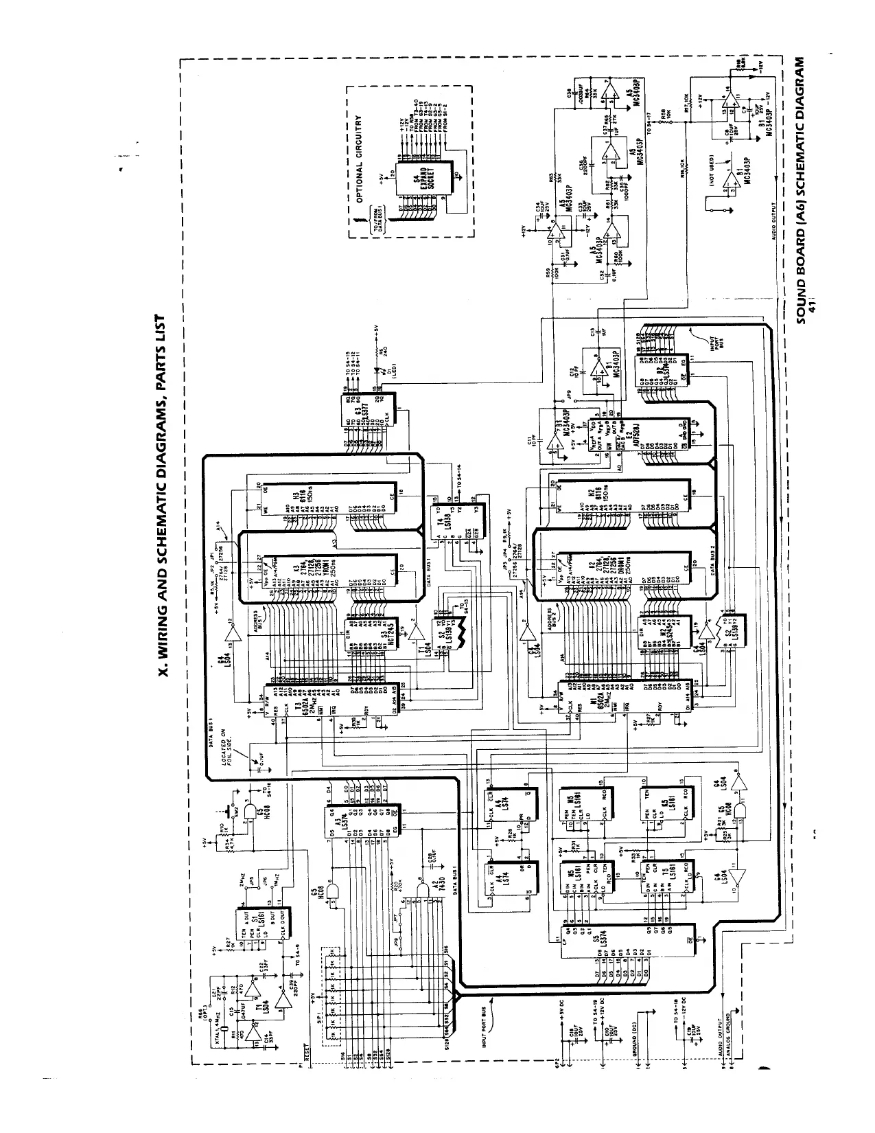
SOUND BOARD (A6) The Sound Board consists of two 6502 microprocessor systems, a dual DAC, input ports to receive commands from the game Control Board, and a low level audio cutput, which is sent to the Auxiliary Power Supply Board for amplification.
The Sound Eoard requires three supply voltages +5V DC, +12V Dc and -12V Dc. In addition a power up reset signal is required from the Control Board.
SYSTEM CLOCK A 4 MHz oscillator is configured with R11, R12, C14, C15, C22, XTAL-1 and Tl. This 4MHz clock is divided py 4 to a 1 or 2 MHz clock for both processors clock input, pin 37 of Nl and T3. A 250 KHz signal from S1 pin 11 is the clock for the programmable timer section consisting of N5, H5, T5 and K5, pin 2.
INPUT CODE LATCH SYSTEM Eight input lines from the Control Board come in on A6P1 and are pulled up by S1Pi and sent to the two input code latches A3 and B2, one for each microprocessor system. A2, pin 8,becomes a logic high when any of it’s inputs are low. this output is connected to pin 11 of the input code latches (A3 and B2). A positive edge at pin 11 causes A3 and B2 to latch the data at their inputs. A2 pin 8 is also connected to the clock inputs of two flip flops, A4 pin 3 and A4 pin 11. When A2 pings goes high, both flip flops are clocked, setting both Q outputs low. The Q outputs, A4 pin 6 and pin 8, are connected to both of the 6502’s active low interrupt request lines, 73 and N1, pin 4. The Q outputs of A4 will stay low until the associated 6502 reads its input port therefore clearing the interrupt.
SYSTEM EPROMS The sound board is designed to accommodate different types of EPROMS. Jumpers JP1, 2, 3, and 4 should be set to the proper position based on the EPROM being used, (See Schematic Diagram).
RESET The Sound Board receives an external reset signal from A1P4 pin 10. This active low reset signal is pulled up by R34 and sent to G5, pin 1 (2-input AND gate). However, if a manual reset is desired, pushing switch sW2 will reset the processor.
MAIN SUMMER The main summer consists of R13 through R17 and Bl, pins 12, 13 and
- Bl pin 14 is the main output from the Sound Board, at A6P2 pin 9, and will swing plus or minus 5V peak to peak.
IX. THEORY OF OPERATION
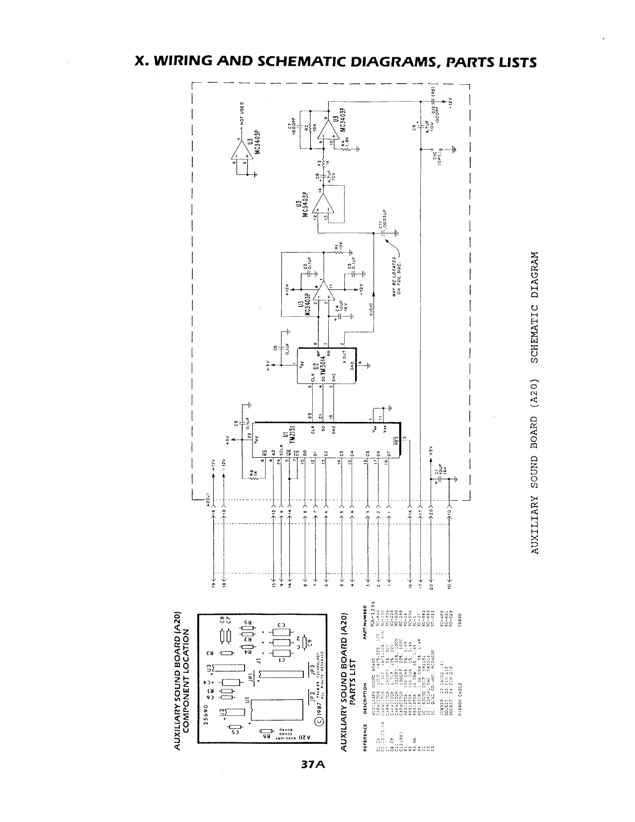
AUXILIARY SOUND BOARD (A20) The Auxiliary Sound Board consists of a YM2151 (U1) sound generator, a YM3014 (U2) DAC, and a LM324 op-amp (U3). The master Sound Board (A6), controls the YM2151 (U1) sound chip by sending commands via the data bus of the master Sound Board’s T3 microprocessor. The YM2151 responds to these commands and serially sends sound data to the YM3014 DAC by means of the CLK, SD, and SH2 lines. The DAC converts this serial data into an analog signal which is buffered and amplified by U3, a LM324 op-amp. This analog signal is then sent back to the main summer of the master Sound Board (A6).
X. WIRING AND SCHEMATIC DIAGRAMS, PARTS LISTS.
TABLE OF CONTENTS
PAGE(S) VIDEO BOARD ASSEMBLY (A1) COMPONENT LOCATION AND PARTS LIST....... 26-27 SCHEMATIC DIAGRAM, SHEETS 1 THRU 8 +28-35
VIDEO CONTROL INTERFACE ASSEMBLY (A8) COMPONENT LOCATION AND PARTS LIST....... 36 SCHEMATIC DIAGRAM sai
AUXILIARY POWER SUPPLY (A5) COMPONENT LOCATION AND PARTS LIST SCHEMATIC DIAGRAM
SOUND BOARD (A6) COMPONENT LOCATION AND PARTS LIST....... 39 SCHEMATIC DIAGRAM. ..-...- esse sees eeeeeee 40-41
CABINET SCHEMATIC/WIRING DIAGRAM SHEET 1 OF 2.. SHEET 2 OF 2. 42-43 ~44-45
TRANSFORMER PANEL SCHEMATIC/WIRING DIAGRAM..... eer 46-47
X. WIRING AND SCHEMATIC DIAGRAMS, PARTS LISTS
VIDEO BOARD ASSEMBLY (A1),
COMPONENT LOCATION
a 7d BWWOr TTPUELTEEET TET HEE PEPE HTLV VMN UHI HH HUH Ke tint boda bot ded ta
VIDEO BOARD ASSEMBLY (Al) PARTS LIST
REFERENCE DESCRIPTION PART NO. Video Board Aesenbly wa-2925 Gapsciter, -0l0P, 480-208, Sov 0-229,
capaci Capacit F, 10%, SOV xo-a34 (UP, 880-208, Sov 40-230 capacitor, 9.20, 20%, 25V 0-127 Octal Transceiver sp" Flip-Flop x0-978 x0-440
X. WIRING AND SCHEMATIC DIAGRAMS, PARTS LISTS
SHEET 1 OF 8 SCHEMATIC DIAGRAM, VIDEO BOARD ASSEMBLY (Ai),
X. WIRING AND SCHEMATIC DIAGRAMS, PARTS LISTS
SCHEMATIC DIAGRAM, SHEET 2 OF 8 VIDEO BOARD ASSEMBLY (A1),
. WIRING AND SCHEMATIC DIAGRAMS, PARTS LISTS
VIDEO BOARD ASSEMBLY (Al), SCHEMATIC DIAGRAM, SHEET 3 OF 8
X. WIRING AND SCHEMATIC DIAGRAMS, PARTS LISTS
ecko ‘22 ey sOLUFXS + ‘cakakskeEtt teat
EE
ipa
VIDEO BOARD ASSEMBLY (Al), SCHEMATIC DIAGRAM, SHEET 4 OF 8
X. WIRING AND SCHEMATIC DIAGRAMS, PARTS LISTS
shisha sii ey iN
VIDEO BOARD ASSEMBLY (Al), SCHEMATIC DIAGRAM, SHEET 5 OF 8
VIDEO BOARD ASSEMBLY (A1), SCHEMATIC DIAGRAM, SHEET 6 OF 8 X. WIRING AND SCHEMATIC DIAGRAMS, PARTS LISTS
X. WIRING AND SCHEMATIC DIAGRAMS, PARTS LISTS
re Ta :
Boy of
gol 42 Esanae
VIDEO BOARD ASSEMBLY (Al), SCHEMATIC DIAGRAM, SHEET 7 OF 8
LE LEIEIIY 22222 aH ze SE eee 8eesss3s
aN> OND eS i Re Ba X. WIRING AND SCHEMATIC DIAGRAMS, PARTS LISTS
SHEET 8 OF 8 SCHEMATIC DIAGRAM, VIDEO BOARD ASSEMBLY (Al),
X. WIRING AND SCHEMATIC DIAGRAMS, PARTS LISTS
VIDEO CONTROL INTERFACE ASSEMBLY (A8) COMPONENT LOCATION
video
CONTROL
INTERFACE
VIDEO CONTROL INTERFACE ASSEMBLY (A8)
REFERENCE
c1,c2
us AgP1 ABP2,A8P3 PARTS LIST
DESCRIPTION PART NUMBER
VIDEO CONTROL INTERFACE ASSEMBLY (A8) MA~1385 CAPACITOR, 0.1UF, +80-20%,50V 0-230 CAPACITOR, 10UF, 16v x0-846 CAPACITOR, .01UF, +90-20%,50V 0-229 RESISTOR, 1K OHM, 5%, 1/4W x RESISTOR PACK, 4.7K OHM X 8 IC, 7418367, HEX BUFFER IC/UP/DOWN COUNTER, 74LS191 Ic, DUAL D FLIP-FLOP, 74LS74 IC, HEX INVERTER SCHMITT TRIGGER HEADER, 16 PIN HEADER, 5 PIN SUPPORT, (4)
X. WIRING AND SCHEMATIC DIAGRAMS, PARTS LISTS
LEFT ROTATE O
LEFT ROTATE
LEFT ROTATE 2
LEFT ROTATE 3
LEFT ROTATE 4
YELLOW LEFT ROTATE 5
LEFT CLEAR
4+5V INPUT
GROUND
RIGHT ROTATE 0
RIGHT ROTATE 1
RIGHT ROTATE 2
RIGHT ROTATE 3
RIGHT ROTATE 4
RIGHT ROTATE 5.
U2 TALSI91
taf Richt cue Loe —A4
VIDEO CONTROL
INTERFACE ASSEMBLY (A8) SCHEMATIC DIAGRAM
This page is a drawing, shown as the original scan.
X. WIRING AND SCHEMATIC DIAGRAMS, PARTS LISTS
| i | ee me i | ee | i | es |
ASPt +12V DC UNREGULATED INPUT
2 ss rr J - - - -- 5 * Our ut i Sy AUDIO | y are AMPLIFIER | 5 LM2002 | cs i i { sogouF ANALOG GROUN: Ra 3 |LOG GROUND 20, 1S
V/2W | s | OnuF |
RS 22 |
aupio oureuT
DC GROUND
LoL ee ne |
AUXILIARY POWER SUPPLY (A5)
COMPONENT LOCATION SCHEMATIC DIAGRAM
PARTS LIST
REFERENCE DESCRIPTION PARTNUMBER AUXILIARY POWER SUPPLY (A5) MA-1395
| c1,c2 | CAPACITOR, 1UF, 10%, 35V, TANT. | x0-715 |
| 3 | CAPACITOR, 1000UF, 25V | X0-874 |
| ca | CAPACITOR, .01UF, +80% -20%, 50V | XO-229 |
| os | CAPACITOR, 0.1UF, +80% -20%, 50V | X0-230 |
| 6 | CAPACITOR, 470UF, 35V | XO~284 |
| RL | RESISTOR, 2.7K Ohm, 5% 1/4W | X0-6 |
| R2,R3 | RESISTOR, 100 Ohm, 5%, 1/4W | X0-28 |
| R4 | RESISTOR, 220 Ohm, 5%, 1/20 | XO-185 |
| RS | RESISTOR, 2.2 Ohm, 5%, 1/4 | X0-595 |
| R6 | RESISITOR, 1 Ohm, 5%, 1/2W | 0-593 |
| UL | AUDIO AMPLIFIER, LM2002 | X0-550 |
HEAT SINK XO~472 12 POSITION CONNECTOR X0-879
X. WIRING AND SCHEMATIC DIAGRAMS, PARTS LISTS
SOUND BOARD (A6) COMPONENT LOCATION
REFERENCE DESCRIPTION
13,037 €8,¢9,c30 18,cis,caa 633/034" AND ‘TaneE ‘UNMARKED CAPACTTORS, eu1,ciz 14,c22 eas ear 28 AND FOURTEEN ONMARKED CAPACITORS e3i,c32 5)
D1 RS, P9,R10, R27, R28, R52 R33, R35, 2S FAL R12 R21, R25, R16, R17, RSS Rie ‘APACITOP,
capactToR, CAPACITOR, CAPACITOR, CAPACITOR, ‘CAPACITOR,
‘caPACITO CAPACITOR, CAPACITOR, ‘CAPACITOR, CAPACITOR, DIODE, HVS: RESISTOR,
RESISTOR, RESISTOR, RESISTOR, RESISTOR, RESISTOR,
PART NUMBER
‘SOUND BOARD ASSEMBLY (AS) Ma-836-Vi01 7 1UF, 20%, S0¥ (NON. POLAR.) X0-746 LovF, 20% 25v (TANTALUM) X0-127
10PF, +80%-208, Sov xo-635 33PF, 108, Loov x0-896 .oa7br, 208, soy xo-638 22PF, 10k, Sov x0-633, O:1UF, +808-208, Sov x0-230
0.30F, 10%, Sov xo-704 1o00rF, 10%, 1007 x0-296 2200PF, 10%, 100v x0-289 00330F, 10%, 00¥ x0-600 220PF," 10%," 100 x0-694 752, (LED, RED) x0-270 1K Ohm, 54, 1/48 x0-5
240 Ohm, 5%, 1/40 xo-173 476 ohm, 58, 1yaH 0-25 3K onm, 5%, 1/40 xO-23 20K ona, 54, 1/40 xO-18 6.aK one, St, 1/40 xo-8 SOUND BOARD (A6) PARTS LIST
REFERENCE DESCRIPTION 20, R94 R61-R62, R63, RES R59, R60 R65, a 23,B2,85 ivy 45,31
SIP 1 sua XTALL AeP1,a6P2 PARTNUMBER RESISTOR, 4.7K ohe, 54, 1/4W x0-7 RESISTOR, 33K ohm, 5%, 1/4 xo-49
RESISTOR, 100K ohm, SM 1/48 x0-45 RESISTOR, 27K ohm, st, 1/4 xO-11 IC, 7430, 8 INPUT NAND GATE 0-649 EC, 7405374, OCTAL "D" FLIP FLOP x0-96 Ic) 740574, ‘DUAL *o" FLIP FLOP xo-434 1G) MC3403P, QUAD OP-AMP xo-333 Ic) 407526), MULTIPLIER oac xo-647 IC, 7418377, OCTAL *D" FUIP FLOP x0-97 Ic) 740s04, HEX INVERTER xonais IC) 74HCOB, QUAD 2 INPUT "AND" GATE x0-872 TC, 6116LP-15, 2K X 8 RAM xo-523 IC) 24LSL61, SYNCHRONOUS PRESETTABLE — x0-440 BINARY COUNTER IC, SPECIFIED PER GAME IC) 74Ls245, OCTAL BUS TRANSCEIVER x0-79 Tc, 6502A, CPU x0-893 Ic, 7418139, OUAL 1 OF 4 DECODER x0-419 TC, 7aHCT245, OCTAL SUS TRANSCEIVER x0-891, IC, 74L5138,'1 OF 8 DECODER x0-437 RESISTOR PACK 8 X 1K O1M 0-493 SWITCH, PUSHBUTTON x0-897 CRYSTAL, 4 MZ x0-366 CONNECTOR x0-879 28 PIN DIP SocKET (2) 0-536 JUMPER, 22 GUAGE (6) x0-469, 20 PIN’ DIP sockET xo-491 m=
My —_—____} roe
LJ
X. WIRING AND SCHEMATIC DIAGRAMS, PARTS LISTS
Black IRD _c1uovRcy IGREEN croswACD VICKET (cert loRANSE «110uRCD ELL caceeneD
ae ineut ‘SOnE/ERZ Becky CIRCUIT GROUND . , 5, PL yorosres wre case dy BRON Goa ERS 200UNC INPUT JUPFERS 2200H0 IREUT JUMPERS [5 _[anarion TRANSFORMER PANEL SCHEMATIC/WIRING DIAGRAM
46 a7
This page is a drawing, shown as the original scan.
sb Z 40 Z MASS ‘WWUOWIG ONIYIM/oTIVNaHOS ZANTEVO sd
precennenny 8 a] fe ¢] Bas ; 000] [ooo] ramus oener—[oool]” | Saset
r Hamer eae)" ne9 exy[' | J ze une Ni09 [ecg] it h te weve | + eran 1 ao 36 s is} |s were ' 6 6] ao 00 . 4 3 3] fs were 0 1 6 é] e020 J) eogeeyr04 an ef fe zeny J
Ls] ae 20 gj ---- 4 |
z| |z + Nae ws! [arg] His] 24°H aunHO wICD) [aud *NG5, We Padi Tee| | le are ue
e| fe — 2078 vo0e og] saner ton eaoTy efoT¥ weeeece-- d
zr ae oath [27
N Naa aaa [sss] ame oA : ab oxiA ANH wot i
"nS “REA
Danse "ORAS “OH
‘anne 20 " si T bso k
e
7 2 10 OTH as ace aaa
s| Sak Wat 31 cvncs [vve]]* | Wot Nr o7on¥
@ wns [eci]|” ‘ab SoM
+ + aos [ezi])* oonei
2 ’ » 2 owes [ind 398] iro orane
1 wes Tas ee]
cw SLSIT SLUWd ‘SINWUDVIC DILWWAHDS GNW DNIUIM *X
This page reads as a drawing: its text was drawn rather than typeset, and comes out in fragments. See the original scan.