Asteroids DP-143-5th-01B
Asteroids (rev 4) (Atari, 1979) · Drawing Package · 1 pages · original scan
CLOCK CIRCUIT
Nore:
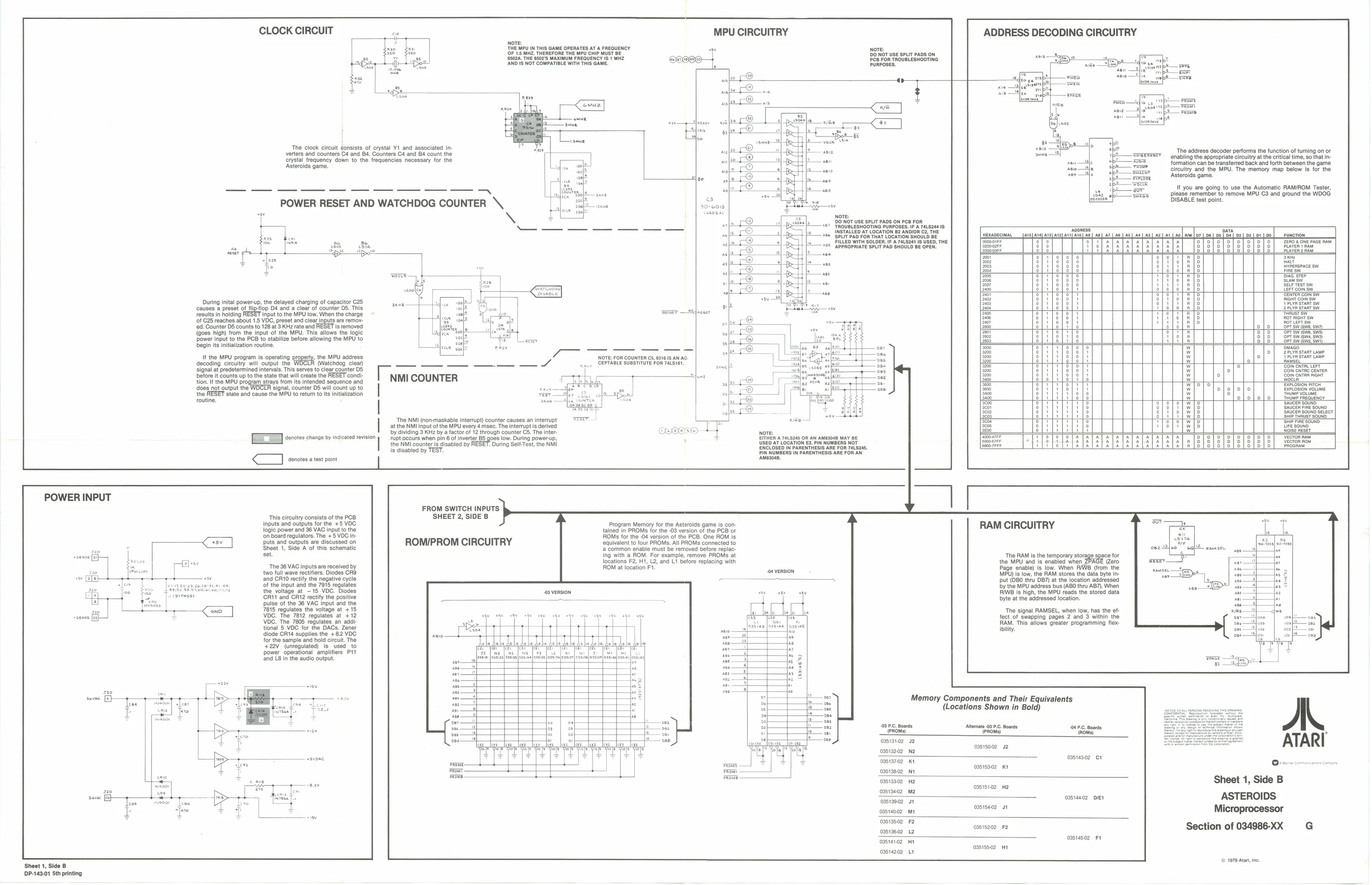
‘The clock circuit consists of crystal Y1 and associated in-
verters and counters C4 and B4, Counters C4 and 64 count the
I frequency down to the frequencies necessary for the Asteroids game.
ee POWER RESET AND WATCHDOG COUNTER \,
wate t i Et Ean
During inital power-up, the delayed charging of capacitor C25 causes a preset of fiptop D¢ and a cla’ of counter DS: This
results in holding input to the MPU low. When the charge =
‘f C25 reaches about 1.5 VOC, preset and clear inputs are remov.
fed. Counter DS counts to 128 at 3 KHz rate and RESET Is removed
{Goes high) from the input of the MPU. This allows the logic Power input to the PCB to stabilize before allowing the MPU to begin its initialization routine.
1 the MPU program is operating propery, the MPU adress decoding circuitry will output the (Watchdog clear)
signal at predetermined intervals. This serves to clear counter DS
before it counts up tot that will create the RESET condi ton the MPU program says from ts intended sequence and does not output the ‘signal, counter D5 will count up to the RESET state and cause the MPU to return to its initialization routine, | ee Tm COUNTER
rer
‘The NMI (non-maskable interrupt) counter causes an interrupt at the NMI input of the MPU every 4 msec. The interrupt is derived by dividing 3 KH2 by a factor of 12 through counter C5. The Inter- ‘upt gecurs when pin of invert BS gos ow. During power up, the NMI countar is disabled by During Self-Test, the NMi is disabled by TEST. ‘denotes change by indicated revision |
onotes a test point ao THE wun Tas QAME oPenaTes AT «FREQUENCY Jr'5 MHZ. THEREFORE THE MPU CMP MUST BE soza, THE 66028 MAXIMUM FREQUENCY IS 1 MHZ ‘AND1S NOT COMPATIBLE WITH THIS GAME” OS MPU CIRCUITRY
Nore: DONOT USE SPLIT PADS ON Pes FoR TROUBLESHOOTING PURPOSES. ADDRESS DECODING CIRCUITRY
Nore EH 7aees on an aMesn4s ay USED AT LOCATION E3 PIN NUMBERS ENCLOSED In PARENTHESIS ARE FOR PLS245, BIN NUMBERS IN PARENTHESIS ARE FOR AN ‘auaaoes. sera 2] ten tie
‘The address decoder performs the function of turing on or enabling the appropriate circutry atthe critical time, so that information can be transferred back and forth between the game circuitry and the MPU. The memory map below is for the Asteroids game.
If you are going to use the Automatic RAMIROM Tester, please remember to remove MPU C3 and ground the WDOG. DISABLE test point.
EEF Con ow
BPLIR START Sw eS oe Sees SSG eefoooe|oooeloooclooo|e eel 3| E|
Ee
‘SAGER sguno stor Star fat SouN lees|eeeeleezaleaealeeze|oa|on2z[>aaanaaa[zzm
POWER INPUT FROM SWITCH INPUTS ‘This circuitry consists of the PCB. SHEET 2, SIDE B Inputs and outputs for the +5 VOC. logic power and 36 VAC Input to the ‘on board regulators. The +5 VDC in- Bbuts and outputs are discussed on Sheet 1, Side A of this schematic set. ROM/PROM CIRCUITRY
The 38 VAC inputs are received by two full wave rectifiers Diodes CRS ‘and CR10 rectly the negative cycle Of the input and the 7815 regulates BRR tte the voltage at ~15 VDC. Diodes oT ovrassy ‘CRI and GAt2 rectly the positive cn pulse of the 36 VAC input and the 7818 regulates the voltage at +15 VOC. The 7812 regulates at +12 VOC. The 7805 regulates an addi tional 5 VDC for the DACs. Zener diode CRTs supplies the +8.2 VOC Program Memory for the Asteroids game is con tained in PROMS for the -03 version of the PCB or OMS for the -04 version of the PCB. One ROM is. equivalent to four PROMS. All PROMS connected to {a common enable must be removed before replacing with a ROM. For example, remove PROMS at locations F2, H1, L2, and Lt before replacing with OM at location F1.
for the sample and hold circuit. The +22V (unregulated) is. used to ower operational amplifiers P11 ‘and LB in the audio output.
are FE pty
Sheet 1, Side B DP-143-01 Sth printing RAM CIRCUITRY
‘The RAM Is the temporary storage space for the MPU and is enabled when Zero, age enable) is low. When RIWB (from the MPU) is low, the RAM stores the data byte input (80 thru OB7) at the location addressed by the MPU address bus (ABO thru ABT). When IWS Is high, the MPU reads the stored data byte at the addressed location.
‘The signal RAMSEL, when low, has the offect of swapping pages 2 and 3 within the RAM. This allows greater programming tlex- ‘bitty,
Memory Components and Their Equivalents (Locations Shown in Bold)
1326, Boats
mai) 2 = aatara toe peceesl [— im wats ng i CT TT o, 03519102 J2 a oxstoce Je
03513702. Kt 03514302 C1
jose
oasis902 He si5102 Ha ossiseoe m2 osstseo2 a1 oasiaeo2 pret ossist02 st oasten02 mt
ossias02 F2 515202 Fe oss19602 2 eng oastes.02 FA osstai02 HY ossisso2 Ht osstez02 Lt Sheet 1, Side B ASTEROIDS Microprocessor
Section of 034986-XX G
© 1679 tat, ne.