Spy Hunter II 2 Player Upright (0B75-00300-0000)
Spy Hunter II (rev 2) (Bally Midway, 1987) · Manual · 36 pages · 30 sections · original scan
SPY HUNTER II U.R.
2 PLAYER
Crelly
MIDWAY MFG. CO.
10601 W. Belmont Avenue Franklin Park, tilinois 60131 / U.S.A. / y
Phone: (312) 451-9200 Cable Address: MIDCO Telex No.: 72-1596
0B75-00300-0000
THIS GAME MUST BE GROUNDED. FAILURE TO DO SO MAY RESULT IN DESTRUCTION TO ELECTRONIC COMPONENTS.
ELECTRICAL BULLETIN: FOR ALL APPARATUS COVERED BY THE CANADIAN STANDARDS ASSOCIATION (CSA) STANDARD C22.2 NO. 1, WHICH EMPLOYS A SUPPLY CORD TERMINATED WITH A POLARIZED 2-PRONG ATTACHMENT PLUG.
CAUTION: TO PREVENT ELECTRIC SHOCK DO NOT USE THIS (POLARIZED)
PLUG WITH AN EXTENSION CORD, RECEPTACLE OR OTHER OUTLET UNLESS THE BLADES CAN BE FULLY INSERTED TO PREVENT BLADE EXPOSURE.
ATTENTION: POUR PREVENIR CHOCS ELECTRIQUES NE PAS UTILISER CETTE FICHE POLARISEE AVEC UN PROLONGATEUR. UNE PRISE DE COURANT OU UNE AUTRE SORTIE DE COURANT, SAUF Si LES LAMES PEUVENT ETRE INSEREES A FOND SANS EN LAISSER AUCUNE PARTIE A DECOUVERT.
CSilly| MIDWAY
OUR TOLL FREE NUMBER FOR
SERVICE INFORMATION CONCERNING THIS GAME, OR ANY OTHER BALLY/MIDWAY™ GAME YOU NOW HAVE ON LOCATION.
CALL US FOR PROMPT, COURTEOUS
ANSWERS TO YOUR PROBLEMS.
Video or Pinball - Continental U.S. 800-323-7182
CS%ally|MIDWAY 10601 West Belmont Avenue Franklin Park, Illinois, 60131 phone (312) 451-9200
©COPYRIGHT MCMLXXXVII BY BALLY MIDWAY MFG. CO. ALL RIGHTS RESERVED.
NO PART OF TH!S PUBLICATION MAY BE REPRODUCED BY ANY MECHANICAL, PHOTOGRAPHIC, OR ELECTRONIC PROCESS, ORIN THE FORM OF A PHONOGRAPHIC RECORDING, NOR MAY IT BE TRANSMITTED, OR OTHERWISE COPIED FOR PUBLIC OR PRIVATE USE, WITHOUT PERMISSION FROM THE PUBLISHER. THIS MANUAL IS FOR SERVICE USE ONLY, AND NOT FOR GENERAL DISTRIBUTION. FOR PERMISSION REQUESTS, WRITE: BALLY MIDWAY MFG. CO., 10601 W. BELMONT AVE., FRANKLIN PARK, IL 60131.
Printed In U.S.A.
BALLY/MIDWAY'S SPY HUNTER II (2 PLYR) U.R. #0B75 ROM/EPROM PART NUMBERS
UNPROGRAMMED 68000 VIDEO BOARD A084-91871-D000 PROGRAMMED 68000 VIDEO BOARD A084-91871-AB75
MIDWAY PART NUMBER
B75A-12610-0000
UNPROGRAMMED SOUNDS GOOD BOARD A084-91863~B000 PROGRAMMED SOUNDS GOOD BOARD A084-91863-AB75
Pos. MIDWAY PART NUMBER U17 B75A-12611-0000 U B75A- = UIs B75A-12613-0000 Us B75A-12614-0000
UNPROGRAMMED TURSO CHEAP SQUEAK A084-91779-B000 PROGRAMMED TURBO CHEAP SQUEAK A084-91779-AB75
M051-00B75-A008 REVISIONS
02-16-87 RELEASE FOR PRODUCTION
SECTION 3
COMPONENT LAYOUTS,
SCHEMATICS & WIRING DIAGRAM
SECTION 3
COMPONENT LAYOUTS, SCHEMATICS & WIRING DIAGRAM
VIDEO INTERFACE AND OUTPUT The red, green, and blue video inputs come into the monitor at P1. Isolation and attenuation is provided by emitter followers Qi, Q2 and Q3. Forced blanking of the video signals 's provided by the circuit of Q4, D5, D6, and D7. The forced blanking causes there to be an interruption in the video signal before it goes to the inputs of IC1. This interruption occurs between scan periods, while retrace is taking place; it is re-
quired by IC1. The forced blanking is not necessary for most
video signals since they already have an interruption cf video (blanking) between scan periods. Some do not; it is to accommodate such signals that the forced blanking circuit is included.
The red, green, and blue signals go into IC1 at pins 2, 4, and
- Their levels are controlled by the gain of separate channels of the contrast amplifier. The gain is controlled by a DC voltage input to pin 11, which varies with the setting of the contrast control.
IC1 provides blanking of the video during retrace in response to blanking pulses at pin 13, derived from the horizontal and vertical sweep circuits. IC1 also requires a gating signal at pin 12 in order to provide red, green, and blue outputs at pins 21, 19, and 17. If the gating signal is not present, IC1 will not provide video output signals. The gating signal comes from IC2, pin 12 and is derived from horizontal sync.
The brightness is varied by varying the DC level of the out-
puts at pins 17, 19, and 21. This is accomplished by varying
the DC voltage input to pin 14. The video outputs from IC1 are provided via R30, R31, and R32 to the neck board where they are amplified by the video output stages Q201, Q202, and Q203 before being applied to the cathodes of the CRT through R10, R11, and R12.
SYNC Sync is applied at P1 (positive sync) or at P2 (negative sync). Composite sync should be applied only to the horizontal syric input of the appropriate polarity. Positive sync is inverted by Q5 and Q6 then applied through D3, D4 and R51 to the sync amplifier Q7. The sync amplifier output is applied through C22, R53, and R55 to pin 14 of IC2. Pin 14 is the sync separation input.
The sync separator extracts the horizontal and vertical sync from each other-providing horizontal sync to the horizontal AFC circuit in the IC. A composite sync output is provided at pin 12. This cutput signal is used for gating IC1 the video interface IC and for triggering the vertical oscillator. HORIZONTAL OSCILLATOR AND OUTPUT The horizontal AFC circuit of C2 receives a horizontal sync input from the sync separator and a feedback signal at pin 1, derived from the horizontal output. Slight differences in frequency and phase of the two signais will cause the AFC to generate a correction voltage at pin 2. The horizontal oscillator inIC2 has its free running frequency determined by the RC time constant of C18, R56, R57, R58, and VR2, the horizontal hold control. The horizonta\ hold control varies the horizontal frequency by varying the RC time constant. Slight correction in frequency is provided by a correction voltage at IC2, pin 3 which comes from pin 2 through R60. The oscillator output at pin 4 is amplified and shaped by the horizontal drive stage Q10. The drive signal is then coupled to the base circuit of the horizontal output transistor Q11 by the horizontal drive transformerT2.T2is used for impedance transformation to provide the Q11 base circuit with the low impedance source that it requires. The horizontal output transistor Q11 is operated as a switch. itis either on or off. It is turned on and off at the scan rate which is determined by the horizontal oscillator frequency which is ultimately determined by the incoming horizontal sync frequency. A yoke current with a sawtooth waveform is needed to deflect the beam linearly across the CRT. The beam begins at the center of the CRT and is deflected from center to right. This center-to-right deflection occurs when Q11 is turned on. The deflection yoke coupling capacitor C38, also known as the S-shaping capacitor, begins to discharge through the yoke; the discharge current causes the beam to be deflected to the right CRT edge. At this time, Q11 is turned off, and the current provided by C38 stops. As the current falls to zero, a voltage is induced across the yoke windings as the magnetic field collapses, an oscillation is produced by the yoke windings and C36, the retrace tuning capacitor. During the first half cycle of oscillation, the induced voltage is impressed on the collector of Q11, C36,
and the primary of they flyback transformer T1. This induced winding. This high voltage is then rectified and applied to the
voltage is stepped up by the flyback transformer’s secondary
high voltage anode of the CRT. When this induced voltage occurs, the electron beam is deflected from the right edge of the CRT face to the left edge. This is called retrace. During the second half cycle of the oscillation (of C36 and the yoke windings), the voltage at the Qi1 collector tries to go negative or below ground. When this happens, the damper diode (include in same package witn Q11) becomes forward biased. The conduction of the damper diode allows energy stored in the horizontal system to decay linearly to zero, thus allowing the beam to return to the center of the CRT face. The focus voltage and the screen, G2, voltage are obtained from the anode voltage with a resistor divider network within the T1 assembly. An auxiliary winding (pin 10) provides feedback.to the horizontai AFC through R71, R70, and C29. This signal is also used to furnish the horizontal blanking input to !C1 via C28, R69, and R68. The signal from the auxiliary winding at pin 5 of T1 is rectified by D14 and filtered to provide the +12VDC supply for the video interface and sync circuits. The auxiliary winding of pins 3 and 4 produces a signal which is rectified by D13 and filtered to produce the +24VDC supply for the vertica! output circuit. The horizontal linearity coil L2 is a magnetically biased coil which shapes the yoke Current for optimum linearity. The horizontal size coil L1 is a variable series inductor which is used to vary the horizontal size of the display.
HIGH VOLTAGE HOLD-DOWN CIRCUIT The high voltage hold down circuit is part of the main PC board P447 of this monitor. The +12V DC supply is sensed via D10. Since the +12V DC supply is flyback pulse derived, the +12V DC supply will rise as the high voltage rises. If the +12V DC exceeds a threshold which is set with VR8, then D12 will conduct, thereby providing drive to IC2, pin 5holddown input of deflection oscillator IC. Tne drive being applied to pin 5 causes the horizontal oscillator within the IC to shut down-thus preventing the generation of high voltage. The horizontal oscillator will remain in its OFF state, even if the input to \C2, pin 5 is removed, unless and until AC power is removed from the monitor input. The power may then be reapplied.
VERTICAL OSCILLATOR AND OUTPUT
The composite sync ouput of IC2, pin 12 is filtered through
the network of R65, C25, C24 and R66 so that only vertical sync is applied to the vertical trigger input at pin 11. The vertical oscillator frequency is controlled by the vertical hold control and its input to pin 10.
The vertical drive output at IC2, pin 7 is applied to pin 4 of IC3, the vertical output IC. Output current from IC3, pin 2 flows through the yoke to cause vertical deflection. During upward deflection, current flows out of pin 2, through the yoke, and into C50 to charge it. Downward deflection is caused by C50 discharging through the yoke in the opposite direction and back into IC3, pin 2. AC feedback is provided through the wiper of the vertical size control VR4 to \C2, pin 8 in order to control the drive amplitude. DC feedback at iC2, pin 9 maintains good vertical linearity at all sizes DC current from the +24V supply flows through R83 and through the yoke to provide downward raster shift. Some of this DC current is diverted from the yoke through the collector of Q9. The amount of this current which is diverted from the yoke can be varied by varying the base drive to QQ by adjusting VR3, the vertical position control, thus providing manual adjustment of the vertical position of the display. The drive signa! at IC3, pin 2 is also used to furnish the vertical blanking input to !C1, pin 13 via R63 and C14.
AUTOMATIC DEGAUSSING ADG The ADG circuit automatically demagnetizes the CRT. This circuit is activated only when the monitor is initially powered up after having beer off for at least 20 minutes. R105 is a positive temperature coefficient device. When it is cold, it has a very low resistance. As it gets warm, its resistance increases. If the monitor is cold when AC power is applied, then R105 with a low resistance allows current to pass through it, D23, D24, and the degaussing coil. As Current flows through R105, it heats up and eventually has a very high resistance, allowing very little current to flow through it. The residual current now flowing through R105 produces a voltage drop across R104 of less than 0.6 volts. This is not enough to forward bias D23 and D24, so there is no current through the degaussing coil. The process of initially having a large current through the degaussing coil and then having the current decay to zero is what produces the degaussing action. The degaussing current decays to zero before the CRT warms up, so the degaussing is completed before the picture comes on.
This page reads as a drawing: its text was drawn rather than typeset, and comes out in fragments. See the original scan.
CROSS REFERENCE LIST
DESCRIPTION
18 pF AK CR 18pF AX CR 33pF AX CR 47pE AX CR 68pF AX CR 100pF AX CR 39GpF AX CR B2GpF AX CR -B1uF AX CR iguF AX TANT 470uF RD ELEC 1g OHM 1/4 5% RES 22 OHM 1/4W 5X RES 47 OM 1/4W 5X RES 68 OHM 1/4W 5% RES 82 OHM 1/4W 5X RES 100 OHM 1/4 5X RES 268 OHM 1/4W 3X RES 476 OHM 1/4W 5X RES 516 OHM 1/4W 5X RES 569 OHM 1/4W 5X RES 688 OHM 1/4W 5X RES 1K OHM 1/4W 5x RES 2K_OWM 1/4W 5X RES 2.7K OWM 1/4W 5X RES 4.7K OHM 1/4W 5% RES
19K OHM 1/4W 5% RES 20K OHM 1/4W 5X RES 1k 9 PIN SIP 4.7K 9 PIN SIP 4.7K 18 PIN SiP 198K 18 PIN SIP 1N4148 DIODE 2N4123 NPN XSTR MPSA7@ PNP XSTR T1P11B NPN XSTR COSC 16MHz COSC 2BMHz 7496 T4ALS2o 7A OR 74F OS 74F 28 7432 TAFTA 7Ar86 74157 TAF 174 7AHCT244 74884 74874 74LS80 74LSB2 74LS95 T4LS08 7AL$28 TALS32 7ALS74 74LS86 74LS148 7418153 74.8157 74LS161 7418163 748169 7ALS173 748174 74L8175 74.8194 TALS244 7418245 7415258 7418273 74L8283 74L8298 74LS368 7ALS374 ary
oe
“ - iu Bau wUwrvanwe Tawa NAnVan
OE NNONNNGH RERUN ON ENON OME ENA ARNE EEN EEE ENON NRE DESIGNATION
C71 ¢55 C72 C37 C38 C73 C75 C51 C74 C45-c5m 39 C53 C54 C76 C77 €2-C33 CP1 CP2 C35 C42 C4 CAL C43 C44 CE6-CES €36 C52 CPL7-151,153-1681 C1 c34 C79 CP3-CP6 R79 RBS REZ RBZ RBS REE R57 R47 R48 R49 REZ R5O R53 ROE REG R96 RO7_RI2H R121 RI2I R92 R99-R112 R56 R64 RIS RI17-R119 R12z R81 RB4 RB7 R68 R71 R75 R76 R77 R78 R58 R1 R3-R6 R1Z R67 R7B R7Z R74 R6G REI R73 R45 R46 R114 RIS R2 RB R11 R51 RS4 RSS RSD R61 R6Z RES RES ROG RED R91 R93 R94 RIS R13 RIG R39 RID RiB-R44 R7 RM7 RMB RMS RMIS RML RM6 RMZ_RM3 RMS RMS 01 D2 Qi a3 Q4 OS G6 a7 ae a9 az aig 1D 1F 1A 12H LIF BK 3G 16D 1K 2F 11H 13¢ 13K 14G 13F 136 5K 12k 144 9A 5A 13A 15B 15¢ 2D
9c 2E 15D 13D 198 154 14D 130 15G 140 19F 148 14¢ 13¢ 7K 3K 11B 128 BA 7A 4K 4H 3H 2H 1H 26 4G 6G 6H OF BF GF 7F 6k 138 88 15H 13H
8G 9H 7H 18G 9G 7G BH 18H SH 11A 12F 30 9E 9D 188 12C 11C 11K 18A 6A 116 126 7B 6B
SE GE 7E 8E 6C 7C BC SC PART NUMBER
9369-29820-9938 B365-29208-2825 8986-99888-9398 B986-99822-2398 G362-B88G0-B028 G362-GH820-5546 G986-08800-3005 B3A5-888 15-0400 2986-99820-2900 9386-09899-0702 2875-20883-2081 188E-G8205-9011 16BE-98885-2916 igge-s9g95-0925 19BE-98995-B829 189E-g9925-9931 198E-28205-9033 188E-99905-9845 19BE-99985-9251 19BE-98985-9052 192E-20005-0054 18ZE-29905-9056 19GE-98805-9961 19BE-99905- 6268 19BE-G9005-807\, 188 -20695-9979
19BE-g9995-2288 199% -82085-9094 192E-80994-2211 192E-99B04-B024 192E-98994-9026 192E-9994-2245 183£-g9g02-2985 184E-20801-6007 1G4E-99B92-8512 194E-99893-2281 199E-ge992-9201 9304-G9804-9687 9386-20893~-7605 @A59-99803-9015 GAS9-28893-2081 GAS9-BG8H3-B434 BA53-B8803-G03E 9304-26893-9959 GA59-28803-6903 GA59-25892-2931 GA59-90803-B804 GAS3-00803-9005 9875-29893-B081 9386-99893-6600 SA15- 68823-9823 9304-96803-2815 @386-99803-7495 GA15-B0803-9011 9986-90893-7305 9586-29803-1994 9386-90893-6100 9986-00803-1095 9986-29893-9900 GA15-90893-2067 BA59-28883-2806 9204-09893-9821 9986-G9883-1923 GAS9-04803-9008 9394-208%3-2823 BA5S9-29803-0093 8204-99893-9024 9304-20803-0025 384-29803-8026 9986-90803-4800 9986-29803-6405 9204-09893-2228 386-99803-4700 394-09803-9038 WAS9-99803-8518 DAES-09293-0811 9286-06803-4600 CROSS REFERENCE LIS
DESCRIPTION
74.8377 PACOUT REV 1 PLA PACNS REV i PLA ROMCTRL REV 1 PLA MMCB2B HAL MMCZ1A HAL MMCB6 HAL MMC@3B HAL COLARB PALZ22L8 IODCD PALIGLS MEMDCD PAL16L8 OTACK PALIGR4 HSYNC PAL16R4 93419 64x9 RAM 2618 2Kx8 RAM 45nS 2818 2x8 RAM 55nS 2864 8KxB RAM 158nS 6116 2Kx@ RAM 158nS 6116 2Kx8 RAM 126nS MCesaae Mc6a4a ROM/EPROMS 16 PIN IC SOCKET(.3) 28 PIN IC SOCKET(.3)
24 PIN IC SOCKET(.3) 24 PIN IC SOCKET(.6) 28 PIN Ic SOCKET(.6)
32 PIN IC SOCKET(.6) 64 PIN IC SOCKET(.9) AUTO INSERT PIN .925 AUTO INSERT PIN .45 FERRITE BEADS JUMPERS. SWITCH PC MTG. DIP SWITCH 18 POS ‘SNAP PC BOARD
RELEASED 19 FEB 1987 6eaee VIDE ABB4~91 MBS 1-9511
ary
ere) ENENRGCOFe NNO OF Neer eye Renee
RAP ME BOARD Daee AI
D165 0 Gs B71
DESIGNATION
12E 11E 59 63 SF alg
14H 14F 15F 14E 15E 9B lg
2k 14k 4A 80 7D 5D 6D 5G 4R AC 4a
4E 1e 1B-38 1¢-3C 7J-183 11D 12D 1G 19 20 2K 14K 14E 15E 110 120 14H 14F 15F 5G §D 6D 7D 8D 9B 13E 49 18-48 1C-4C 73-180 11D 120 1E 4A 73-189 4E 92 93 94 95 36 v1 FB1-FBI8 gW1-JW12 PBL PBZ 12A a2 ag PART NUMBER
BAS9-99803-9012 AS9A-26AXL-AXHD ABSSA~26AXL-BXHD AS9A-26AXL-CXHD 8986 -99803-3950 9386 -28803-8989 9996-99803-9285 9986-29803-9188 GE61-98892-0901 9875-G9893-£003 9875-BG803-B004 6875-9o803-9005 8B75-26803-9086 B986-B0822-9655 BA59-99883-B928 GAS9-98893-9029 GA15-99893-0879 BA59-29283-0827 GA59-08892-g914 8394-99893-2051 BAi5-99803-9568 SEE _ROM/EPROM CHART 119£-89991 -0093 118E-99901-9985
11B€-92901-9029 119-99991-9987 118E-99981-9012
L1GE-99901-B924 11BE-99981-2016 9304-99804-9009 B304-29804-9919 8316-29894-2952 L17E-998081-Ba99 G986-22804-3155 113E-99291-950 6817-98887-813 Ag8g-9187\-CoB DESIGNATION LIST:
DESIGNATION
cPi-2 cRt3-6) CPt7-1511 cPL153-1681
Caz c43-caa Ca5-c5o cei C52 c53-c54 C55 C56-c69 ca c71-c72 c73 C74
676-C77 RL R2 R3-R6 R7 RB RS-R1D Ril R12 R13-R44 RAS-R4G RA7-R49 Roo R51 R52 R53 R54-R55 R56 R87 R58 R59 Roe R61-R63 R64 R65 REG Rev R68 R69 R7 R71 R72 R73 R74 R75 R7G-R78 R73,R8S R81 R82,RO3 Red R85, REE R87 Reg-Re9 Ro R91 R92 R9S-R9S R96-R97 R98 R99-R112 R113 R1i4-R115 R116 RI17-R119 DESCRIPTION
39BpF AX CER 47BuF RD ELEC Blur AX CER O1uF AX CER iguF AX TANT 18BpF AX CER Buf AX TANT 39pF AX CER «BluF AX CER 18pF AX CER 68pF_AX CER 823pF AX CER 39%pF AX CER B2BpF AX CER A7pF AX CER 33pF AX CER S1uF AX CER 68pF AX CER 1BpF_AX CER B2pF AX CER 18uF AX TANT \gpF AX CER 18pF AX CER 33pF AX CER 18pF AX CER 6BpF AX CER 4K OHM 1/4W 5X RES 4.7K OHM 1/4W 8X RES 1K OM 1/4W 5% RES 20K OHM 1/4W 5X RES 4.7K OHM 1/4W 5% RES \OK OHM 1/4W 5X RES. 4.7K OHM 1/4W 5X RES 1k OKM 1/4W 5X RES 18K OHM 1/4W 5X RES 2.7K OHM 1/4W 5X RES 47 OHM 1/4W 5X RES 68 OHM 1/4W 5% RES 4.7K OHM 1/4W 5% RES 47 OHM 1/4W 5x RES 68 OHM 1/4W 5x RES 4.7K OHM 1/4W 5% RES 208 OHM 1/4W 5X RES 22 ORM 1/4W 5X RES 689 OHM 1/4W 5X RES 4.7K OHM 1/4W 5X RES 82_OHM 1/4W 5X RES 4.7K OHM 1/4W SX RES 288 OHM 1/4W 5% RES 4.7K OHM 1/4W 5x RES 2K OHM 1/4W 5x RES AK OHM 1/4W 5X RES 518 OHM 1/4W 5X RES 2K OHM 1/4W 5X RES 1K OKM 1/4W 5X RES 519 OHM 1/4W 5X RES AK OHM 1/4W 5X RES 2K OHM 1/4W 5% RES 1K OBM 1/4W 5X RES 518 OHM 1/4W 5X RES 568 OHM 1/4W 5X RES 1 OHM 1/4W SX RES 478 OHM 174W 5X RES 18 ORM 1/4W 5X RES 478 OHM 1/4W_ 5X RES 18 OHM 1/4W 5X RES 478 OHM 1/4W 5X RES 4.7K OHM 1/4W SX RES 68 ORM 1/4W 5% RES 4.7K OHM 1/4W 5% RES 188 OHM 1/4W 5% RES. 4.7K OHM 1/44 5X RES 82 OHM 1/4W 5% RES 288 OHM 1/4W 5x RES 1@B OHM 1/4W 5X RES. 4.7K OHM 1/4W 5X RES 2.7K OHM 1/4W 5X RES 4.7K OHM 1/4W_ SX RES 288 OHM 1/4W 5X RES DESIGNATION
R12g-R121 R12 R123 RML RM2-RMS RM6 RM7-RM1 D1 Qi a2 a3 aa aig Ic Ic IC 1c Ic Ic I¢ Ic 1c Ic Ic Ic Ic 1c IC IC Ic Ic 1c Tc: Ic Ic Ic 1c Ic 1c Ic Ic Ie Ic Ic Ic 1c Ic IC 1c Ic Ic 1c Ic IC Ic Ic Ic Ic Ic Ic IC Ic Ic Ic 1c Ic It Ic IC Ic 1c 1c Ic Ic Ic IC Ic Ic 1c a3
1A 1B 1c 1D 1E 1F 1g 1H 1g ik
2c
2E 2F 2G 2H 2d 2k
3c 3G 3H
3k 4A 4B 4c
4g 4H
4k 5A 3B 5C 5D BE SF
5H 5J 5K 6A 6B 6c 6D 6E oF 6s 6H
6K 7A
7c 7D 7e 7F
7H
7k BA
ac DESCRIPTION
82 OHM 1/4W 5X RES 208 OHM 1/4W 5% RES 82 OHM 1/4W 5X RES 4.7K 9 PIN SIP 198K 19 PIN SIP 4.7K 19 PIN SIP 1K 9 PIN SIP 1N4148 DIODE 2N4123 TIPLIS 2N4123 Ama TIPLIS. 7496 PROGRAM ROM/EPROM PROGRAM ROM/EPROM 16MHz OSC MC6a4e 2aMHz OSC 74LS368 74LS161 PAL1BL@ IovcD1 7432 PROGRAM ROM/EPROM PROGRAM ROM/EPROM TAS74 74LSB5 THETA 748161 7418157 PALI6L8 MEMDCD1 PALIGR4 DTACK1 PROGRAM ROM/EPROM PROGRAM ROM/EPROM TAF OS 7418157 74LS245 74LS148 93419 2064 BKx8 RAM 2064 8KxB RAM Mcessag 74163 7ALS157 6116 2x8 RAM 74LS157 TAHCT 244 7aLsee 7ALS374 2618 2x8 RAM 7ALS374 74LS377 2818 2Kx8 RAM 7ALS244 74L8377 74F 157 74LS273 74LS298 7ALS374 2618 2kxB RAM 7ALS374 7ALS169 7418163 74L8i63 74L8377 74L8173 74LS157 7418298 7ALS374 2818 2kx8 RAM 74LS374 748169 7aLS194 7ALS194 FGo ROM/EPROM 74LS86 748157 748174 74LS374
68098 VIDEO GAME BOARD Age4-91871-Da98 M@51-28114-D165
DESIGNATION LIST:
DESIGNATION DESCRIPTION DESIGNATION DESCRIPTION
| Ic 8D | 2818 2Kx8 RAM | FB1-FB1B | FERRITE BEAD |
| IC 8E | 74LS374 | PB1-PBZ | SWITCH PC MTG. |
| IC BF | 748169 | OW1-OW12 | QUMPER WIRE |
| IC 8¢ | 745194 | a1 | AUTO INSERT PINS .845 |
| IC 8H | 74LS194 | 92-96 | AUTO INSERT PINS .825 |
| IC 80 | FG1_ROM/EPROM | a2,019 | SNAP |
| IC 8K | TAF OB | PC BOARD | Agee-91871-Ccaae |
IC 9A 74HCT244 Ic 9B PAL2@L8A COLARB1 Ic 9c 7ALSB2 Ic 9D 74LS258 IC 9€ 7ALS258 IC 9F 7418169 IC 9 74LS194 IC 9H 74LS194 Ic 99 FG2_ROM/EPROM IC 184 74.8273 IC 198 748273 Ic 19C 74886 Ic 190 74728 IC 19E 74LS20 IC 19F 74LS74 IC 196 748194 IC 18H 74LS194 Ic 190 FG3_ROM/EPROM IC 11A 7ALS244 I¢ 118 74L8153 Ic 11¢ 74LS273 Ic 11D BGS _ROM/EPROM I¢ 11E 74L8377 IC 11F TAF OB Ic 116 74LS283 IC 11H TAF 74 IC 110 825153 ic 11K 74LS273 IC 12A, 1g POS DIP SWITCH IC 12B 74/8153 Ic 12¢ 74L8273 Ic 12D BG1_ROM/EPROM IC 12E 74L8377 IC 12F 74LS245 Ic 126 7ALS283 I¢ 12H 74ALS28 IC 120 828153 PACNS PLA I¢ 12k TAF 174 IC 134 74HCT244 Ic 13B 74LS174 IC 13 7486 Ic 130 74LS28 IC 136 6116 2Kx8 RAM IC 13F 74F 157 IC 136 74F157 IC 13H 74L8174 Ic 130 74L832 IC 13K 74786 IC 144 7AHCT244 IC 14B 74LS74 Ic 14c 7ALS74 Ic 14D 74LS32 It 14E MMC@6 HAL IC 14F MMCB2B HAL IC 146 74F 157 IC 14H 825153 IC 140 7ALS74 IC 14K PAL16R4A HSYNCI IC 154 7ALS2o IC 15B 74884 Ic 15¢ 74884 Ic 15D 74LSB8 IC 15E MMC3B HAL IC 15F MMCS1A HAL IC 15G 7ALS74 IC 15H 7ALS174 IC 150 74LS175
RELEASED 18 FEB 1987 RAP Dip SHITCH METER CONTROL oureuT PoRTS
INPUT PORTS
DTACK CONTROL
INTERRUPT CONT,
SPARE GATES
RESET
WoRIz, CLOCKS watch Dos FOREGROUND coum ence SECTION OLOR RAM
COLOR DRIVE
‘BackGROUND
BRCKGROUND
TIME Base,
Tike rort™S8do DALY MIDWAY HFG. CO. 60000 VIDEO GANE BOARD ‘OF 19 [REV
[SHEET 4
R.A. PLoUSSARD,
iz fe 1907
Last USED! R129/C77/ Jut2, 010, De, RHI@/FB16/CP160
crise
Nov usEDr
“09 “am Ammar ATE
severe an ssirgda 9 a oF Hasame
T ab tegt-estada
OlL-€ i
This page carries no recoverable text. It is a drawing or a photograph. See the original scan.
This page carries no recoverable text. It is a drawing or a photograph. See the original scan.
This page carries no recoverable text. It is a drawing or a photograph. See the original scan.
3-14
3-15
T $83 4883 iA5 Cy ET En = ;
= Te 3017 26
‘s
rae 4888 as {beats em CIE] = “eePRzZ ays v 7885 038
3-16
DOLLY IBUAY FE. CO.
eae! aicer 16 oF 9 [eee
GYBLNK. CHPBLNK
2ausis7 [WOYES7 Gary wip wa con ‘ores BALLY MIDHAY HFG. CO.
|n. 8. PLoussaRn} Fe 10 1967 | cee00 VIDEO GAME BOARD SHEET 19 OF 19 [REV
3-17
° SOUNDS GOOD = A084-91863-B000 1 M051-00114-B151 i | | | 4 r Hy lg =
| | Ale | ¢ | 2 | |
| sia} | 22), | 4 | DESIGNATION LIST |
| 2 | fd | wo |
RG ¢
| | \é | 2 | DESIGNATION | DESCRIPTION |
if jt
| 7 | 3 | CP1-CP7,CP9-CP13 | -O1MF AX CER. | |||
| g | i. | © 6 | CP14,CP15 | 10MF AX TANT. | ||
| 8 | Hoty | z ° | cP16 | 1OOMF AX ELECT. | ||
| g | S| | sao | CP101,CP102 | 0.1UF AX CER. | ||
| Z | : | zoa | C1,C2 | 390PF AX CER. | ||
| 3 | are | C3-C5 | LOOPF AX CER. | |||
| a | o | C6,C7 | 820PF AX CER. | |||
| 5 | ° | >0@ | C8-C11 | 1OOPF AX CER. | ||
| dt, | <a | rom | 8 | aca | C101 C102 | 390PF AX CER. | |
| «Bee F | a | est | C103 | MF RD TANT. | ||
| Bee + | EB | 3 | Woo | C104 | .O1MF AX CER, | |
| nae | 5 | S | n°O | C105 | 47MF AX ELECT. | |
| : | Fu. | + we | Z | << | C106 | 680PF AX CER. |
| 1 | 1 | 8 | 107 | O1MF AX CER. | ||
| + | 4 | ol | C108 | 1MF RD TANT. | ||
| i-— | . | 5| | C109 | 68PF AX CER 10% | ||
| ‘ | C110 | .01 MF AX CER. |
c111 150PF AX CER 10% C112 470 PF AX CER 10% c113 270 PF AX CER 10% cia 1MF RD TANT.
| x | c115 | S600PF AX CER 10% | ||
| S) | ® | C116 | .O1MF AX CER. | |
| zorao | 2 | . | C117 | IMF RD TANT. |
| al | false | c118 | 270PF AX CER 10% | |
| = | alo | c119 | 1OMF RD TANT. | |
| olf | lay | c120 | -O1MF AX CER. | |
| 5 | LES | c121 | 1OMF RD TANT. | |
| < Ie, | 122 | 47MF AX ELECT. | ||
| Logo | 2 ge | c123 | 1OOMF AX ELECT. | |
| — | sw | 2 |e: | c301 | 150PF AX CER. |
| g ae | C302,,C303 | 470PF AX CER 10% | ||
| : | a | 304 C307 | O0.1UF AX CER. |
By R1-R3 4.7K OHM 1/4W CRBN,
| _—r | R4 | 10K OHM 1/4W CRBN. | |
| a | R5 | 100K OHM 1/4W CRBN. | |
| + goon BE | R6-R7 RO | 4.7K OHM 1/4W CRBN. | |
| TE 7883 | 3 | R10 | 1K OHM 1/4W CRBH. |
| ao | R12-R14 | 4.7K OHM 1/4W CRBN. | |
| — | R15,R16 | 10K OHM 1/4W CRRN. |
R17, R18 100 OHM 1/4W CRBN. R19-R21 10K OHM 1/4W CRBN.
3-18
SOUNDS GOOD A084-91863-B006 M051-00114-B151 DESIGNATION LIST DESIGNATION LIST
| DESIGNATION | DESCRIPTION | DESIGNATION | DESCRIPTION |
| R22 | 100K OHM 1/4W CRBN. | 14 | 74F 32 |
| R23 | 10K OHM 1/4W CRBN. | U15 | SGO1RO PAL |
| R24 | 100K OHM 1/4W CRRN. | U16 | RAM 2K X 8 |
| R25 | 100 OHM 1/4W CRBN. | U17 ,U18 | ROM/EPROM |
R26 47K OHM 1/4W CRBN.
| R101 | 12K OHM 1/4W CRBN. | FB1,FR2 | FERRITE BEAD |
| R102 | 160K OHM 1/4W CRRN. | FB101,F8102 | FERRITE BEAD |
| R103 | 100 OHM 1/4W CRBN. | FB301 | FERRITE BEAD |
R104 330K OHM 1/4W CRBN.
| R105 | 24K OHM 1/4W CRBN. | ICS U5 | 64 PIN IC SOCKET |
| R106 | 3.3K OHM 1/4W CRBN. | ICS U6 | 24 PIN IC SOCKET .600 |
| R107 | 24K OHM 1/4W CRBN. | ICS U7,U8 | 28 PIN IC SOCKET |
| R108 | 150K OHM 1/4W CRBN. | ICS U9 | 40 PIN IC SOCKET |
| R109 | 82K OHM 1/4W CRBN. | ICS U10 | 16 PIN IC SOCKET |
| R110 | 510K OHM 1/4W CRBN. | ICS Ui5 | 24 PIN IC SOCKET .300 |
| R111,R112 | 120K OHM 1/4W CRBN. | ICS U16 | 24 PIN IC SOCKET .600 |
| R113 | 33K OHM 1/4W CRBN. | ICS U17,U18 | 28 PIN IC SOCKET |
R114 330K OHM 1/4W CRBN.
| R115 | 150K OHM 1/4 CRRN. | a | AUTO INSERT PIN TIN .025 SQ. |
| R116 | 33K OHM 1/4¥ CRBN. | J2 | AUTO INSERT PIN TIN .045 SO. |
| R117 | 18K OHM 1/4W CRBN. | 33 | AUTO INSERT PIN TIN .025 SQ. |
R118 100K OHM 1/4W CRBN.
| R119 | 510K OHM 1/4W CRRN. | JW1-JW3 | ZERO OHM RESISTOR |
R120 47K OHM 1/4W CRBN.
| R121 | 1K OHM 1/4W CRBN. | LED 1 | GREEN LED |
R122 2.7K OHM 1/4W CRBN.
| R123,R124 | 360 OHM 1/4W CRRN. | sw | SWITCH PC MTG. |
R125 180 OHM 1/4W CRBN.
| R126 | 2.7K OHM 1/4W CRRN, | Y1 | 16 MHZ XSTAL OSC. |
R127 560K OHM 1/4W CRBN. R202 100 OHM 1/4W CRBN. M1 NOT INSERTED D3-D4 1N5817
Q1-03 2N5305
Ul MC 3340 U2 U3 LM359 US 68000G8 CPU U6 RAM 2K X 8 U7,U8 ROM/EPROM ug 6821 P.T.A, u10 AD7533JN DAC 11 14584 /40106 Ui2 74874 u13 74LS04 CROSS REFERENCE DESCRIPTION
68 PF AX CER 10% 100 PF AX CER 150 PF AX CER 10% 270 PF AX CER 10% 390 PF AX CER 470 PF AX CER 10% 680 PF AX CER 820 PF AX CER 5600 PF AX CER 10% -O1 MF AX CER
0.1 UF AX CER 1 MF RD TANT 10 MF AX TANT 10 MF RD TANT 47 MF AX ELECT 100 MF AX ELECT 100 OHM 1/4W CRRN
180 OHM 1/4W CRBN 360 OHM 1/4W CRBN 1K OHM 1/4W CRBN 2.7K OHM 1/4W CRBN 3.3K OHM 1/4W CRBN 4.7K OHM 1/4W CRBN
10K OHM 1/4W CRBN
12K OHM 1/4W CRBN 18K OHM 1/4W CRBN 24K OHM 1/4W CRBN 33K OHM 1/4W CRBN 47K OHM 1/4W CRBN 82K OHM 1/4 CRBN 100K OHM 1/4W CRBN 120K OHM 1/4W CRBN 150K OHM 1/4W CRBN 160K OHM 1/4W CRRN 330K OHM 1/4W CRBN 510K OHM 1/4W CRBN 560K OHM 1/4 CRBN
1N5817
2N5305
74LS04 74F 32 al Fos) N OPANHNHE ANNNNSA NEN PwOAN MN [3
PNNENNFENNNEE
i) DESIGNATION
C3-C5,C8-C11 C111,C301 c113,C118 C1,C2,C101,C102 C112,C302,C303 C106 C6,C7 C115 €104,c107,c110 €116,C120,CP1-cP7, CP9-CP13 304 ,C307 ,CP101 ,cP102 C103,C108,C114,C117 cP14,CP15 C119,C121 €105,C122 CP16,C123 R17,R18,R25,R103, R202 R125 R123,R124 R10,R121 R122,R126 R106 R1-R3,R6-R7,R9 R12-R14 R4,R15,R16,R19-R21, R23 R101 R117 R105,R107 R113,R116 R26 ,R120 R109 R5,R22,R24,R118 R141,R112 R108,R115 R102 R104,R114 R110,R119 R127
D3-D4
Q1-03
U13 u14 PART NUMBER
0307-00800-011 0304-00800-0001 0307-00800-0010 0307 -00800-0009 0986-00800-3000 0307-00800-0008 0358-00800-0002 0304-00800-0002 0307-00800-0007 0986 -00800-2200
0986-00800-0200 0307-00800-0004 0986-00800-0700 0307 -00800-0005 0307-00800-0003 0307-00800-0006 100E-00005-0033
100£-00005-0039 100 -00005-0048 100E-00005-0061 100E-00005-0071 100E-00005-0074 100E-00005-0079
100E -00005-0088
100E -00005-0090 100E-00005-0093 100E -00005-0097 100E-00005-0100 100E -00005-0104 100E-00005-0112 100£-00005-0115 100E-00005-0118 100E-00005-0120 100£-00005-0121 100E -00005-0128 100E-00005-0133 100E-00005-0134
103£-00003-0009
0360-00802-0012
0304-00803-0060 0304-00803-0059
3-19
CROSS REFERENCE
DESCRIPTION
TAS74 14584/40106 6821 PIA 68000G8 CPU AD7533JN DAC SGO1RO PAL LM359 MC3340 RAM 2KX8 ROM/EPROM ROM/EPROM ROM/EPROM ROM/EPROM
FERRITE BEAD
16 PIN IC SOCKET 24 PIN IC SOCKET .300 24 PIN IC SOCKET .600 28 PIN IC SOCKET 40 PIN IC SOCKET 64 PIN IC SOCKET
AUTO INSERT PIN TIN .025 SQ AUTO INSERT PIN TIN .025 SQ AUTO INSERT PIN TIN .045 SQ ZERO OHM RES
GREEN LED SWITCH PC MTG 16 MHZ XSTAL OSC PC ROARD
6-13-86 Released for Production, CMM. Foy PRPBE REN BER E FE ~<
PRPaANPR
foo)
Pee SOUNDS GOOD A084-91863-B000
MO51-00114-B151
DESIGNATION
ull U9 Us u10 ULS U2,U3 UL N6,U16 U7 us UL7 u18
FB1,FB2,FR101,FB102, FB301 ICS U10 ICS U5 ICS U6,U16 ICS U7,U8,U17,U18 Ics U9 Ics US
Jl
J3
J2
JW1-JW3
LED 1 Swi Y1
6+86 Rev. 1.0 CMM - Changed R101 from 24K to 12K. 6-2 8-05-86 Rev. 2.0 CMM - Removed D1. 8-2 8-86 Rev. 3.0 CMM - Changed C301 from 330PF to 150PF. PART NUMBER
0304-00803-0061 0304-00803-0056 0304-00803-0054 0304-00803-0051 0304-00803-0055 0E36-00803-0009 0304 -00803-0053 0358-00803-0002 0304-00803-0057
SEE ROM/EPROM CHART
0316-00804-0002
110E -00001-0003 110E£-00001-0009 110€-00001-9007 110£-00001-0010 110£-00001-0011 110£-00001-0016
0304-00804-0009
0304-00804-0009
0304-00804-0010
117£-00001-0003
119£-00001-0001 0986-00804-3100 §304-00804-0008 A080-91671-G000 a Hite RC ha Hue "gate? ap,
aa 088 LPs te :
i. BALLY WIDMAY HFG. CO.
_ tthe he
Qi 2 > mH
we we
3-21
SPARE GATES
pi HesBeaLE SS ae aa aa as
[SHLD GND vy ani 1ye ncisies —zu.s0e | 168817 a RESET~ 16)
RESET~
[mes 5 Pe 2 T lL age via
appress, Data ‘CONTROL, REV 2 ~ Changed C201 to 150 PF. 8/29/06 Chm
REV 1 ~ REROVED Di, 974/06 CHM
NOTES ALLY MIDUAY . C. NEDNICK be EN IFS. OO. sounps Goon ead—91969-ne0e nesi—00114-P152 [size 2 OFS [REN
erese/sie e7esersie
ae vec Jar sno]
Tsfale|"]a]5)~ eRe P Perel NOTES C. MEDHICK T PER ‘sounBs G00D Te JUNE 6 @04-91969-2008 Wo51-00114-2152 RALLY MIDUAY HFS. CO. [SHEET 3 OF 5 [REV
3-22 7aLs04 nos 12 vis RESETIA4 IPL 38 oo
- 1 £ a9 oe ‘SHDSELE
G. MEDNICK Tree 18 JUNE BE SHY 4 oF S[ReW
07599 2 va REF J3 ~ 12 PIN KK108 an [PDs 5 $ [Pn 6 Upp we ft» : ne omseonl > Key 39 3332 BVSENSE 55 1 AVARETURN F399 REV 1.0 6-26-96 R101 CHANGED TO 12K. CHM
NOTES? i a BALLY MIDUAY HFG. CO.
T PER 10 JUNE 66 SHEET SOF 6 [REV
cen = (©1985 BALLY MIDWAY MPD: CO. ALL RIGHTS bie » AEE il ve taa0)
THIS DWG IS CONFIDENTIAL & PROPERTY OF BALLY/MIDWAY MFG_CO Cstilty [MIDWAY wre. co.
FRANKLIN PARK, Ik 60131
DIM. TOLERANCES . sO UNLESS OTHERWISE SPEC CONCENTRICITY TLR. 002 FRACTIONAL 7 Bpies-T™ DECIMAL : TURBO CHEAP SQEAK
A084-91779-B000 DO NOT SCALE DWG. a
$25NG RV - Chang
10-31-& 5 pat Roburon (PHRS REVISIONS PART NO IMO-5:| -0-0-1-1°4 -Prl-2:6 SHEET _/ of f M051-00114-8163 TURBO CHEAP SQUEAK A084-91779-B000 (Rev. 1)
DESIGNATION LIST.
DESIGNATION
Cl c2-C3 C4&-C9 C37 c10 Cll c12 C13 C14 cis c16 C17 C18 c19 c20 Cal c22 C23 C24 C25 C26 C27 C28-C29 c30 €31-C€34 C35-C36
R10 R11-R12 R13-R16, R62 R17 R18 R19 R20 R21 R22 R23 R24 R25 R26 R27 R28 R29 R30 R31 DESCRIPTION <OLMF AX. CR. 18PF AX. CR. 820PF AX. CR. 1OOPF AX. CR. 10MF RD TANT -O1MF AX. CR. 47MF AX. ELECT. sO1MF AX. CR. 270PF AX. CR. 1MF_RD TANT .O056MF AX. CR. 270PF AX. CR. 1MF RD TANT 470PF AX. CR. 150PF AX. CR. AMF RD TANT 10MF AX TANT 680PF AX. CR. -O1MF AX. CR. 47MF AX. ELECT. IMF RD TANT 68PF AX. CR. «O1MF AX. CR. 1QMF RD TANT 390PF AX. CR. 470MF AX, ELECT.
4.7K OHM 1/4W 5% 3.3K OHM 1/4W 5% 150 OHM 1/4W 5% 4.7K OHM 1/4W 5% 100 OHM 1/4W 5% 47K OHM 1/4 5% 100 OHM 1/4W 5% 10K OHM 1/4W 5% 100K OHM 1/4W 5% 10K OHM 1/4W 5% 100K OHM 1/4W 5% 10K OHM 1/4W 5% 4.7K OHM 1/4W 5% 47K OHM 1/4W 5% 360 OHM 1/4W 5% 2.7K OHM 1/4W 5% 180 OHM 1/4W 5% 360 OHM 1/4W 5% 120K OHM 1/4W 5% 330K OHM 1/4W 5% 4.7K OHM 1/4W 5% 510K OHM 1/4W 5% 120K OHM 1/4W 5% DESIGNATION
R32 R33, R34 R35 R36 R37 R38 R39 R40 R41 R42 RAZ R44 R45 R46
R47 R48 R49 R60 R61
Ql 02-04
ul v2 U3 U4 U5 U6 W7 U8 ug u10 ULL u12 U13 u14 Ui5
Ics U3 ICS U4-U6 Ics U10 Ics Ull
FRL-FR4 pL -JWs Swi DESCRIPTION
33K QHM 1/4W 5% 18K OHM 1/4 5% 110K OHM 1/4W 5% 33K OHM 1/4W 5% 150K OHM 1/4W 5% 82K OHM 1/4W 5% 510K OHM 1/4W 5% 150K OHM 1/4W 5% 24K OHM 1/4W 5% 3.3K OHM 1/4W 5% 12K OHM 1/4W 5% 330K OHM 1/4W 5% 160K OHM 1/4W 5% 100 OHM 1/4w 5% 560K OHM 1/4W 5%
24K OHM 1/4W 5% 4.7K OHM 1/4W 5% 2.7K OHM 1/4W 5% 100 OHM 1/4W 5% 1K OHM 1/4W 5%
MPS3646 2N5305
C1K OSC 74LS76 68B09E EPROM/ROM EPROM/ROM 2k X 8 RAM 7418139 74LS02 74LS00 68821 AD7533 40106 L359 LM359 3340,
40 PIN IC SOCKET 28 PIN IC SOCKET 40 PIN IC SOCKET 16 PIN IC SOCKET
FERRITE BEAD Perea HaRE
DESIGNATION DESIGNATION LIST
DESCRIPTION
GREEN LED CLOCK OSCILLATOR 8MHZ 9 PIN KK100 R/A 12 PIN KK156 R/A 12 PIN KK100 R/A SPACERS TURBO CHEAP SQUEAK CROSS REFERENCE
DESCRIPTION
18PF AX. CR. 68PF AX. CR. 100PF AX. CR. 150PF AX. CR. 270PF AX. CR. 390PF AX. CR. A70PF AX. CR. 680PF AX. CR. 820PF AX. CR. -OO56MF AX. CR. -OAMF AX. CR.
1MF RAD TANT 10MF AX TANT 10MF RAD TANT 47MF AX. ELECT 470MF AX. ELECT
100 OHM 1/4WATT 5% 150 OHM 1/4WATT 5% 180 OHM 1/4WATT 5% 360 OHM 1/4WATT 5% 1K_OHM 1/4WATT 5% 2.7K OHM 1/4WATT 5% 3.3K OHM 1/4WATT 5% 4.7K OHM 1/4WATT 5%
10K OHM 1/4WATT 5%
12K OHM 1/4WATT 5% 18K OHM 1/4WATT 5% 24K OHM 1/4WATT 5% 33K OHM 1/4WATT 5% 47K OHM 1/4WATT 5% 82K OHM 1/4WATT 5% 100K OHM 1/4WATT 5% 110K OHM 1/4WATT 5% 120K OHM 1/4WATT 5% 150K OHM 1/4WATT 5% 160K OHM 1/4WATT 5% 330K OHM 1/4WATT 5% 510K OHM 1/4WATT 5% 560K OHM 1/4WATT 5%
MPS3646 2N5305, M051-00114-B163 TURBO CHEAP SQUEAK A084-91779-B000 (Rev. 1)
| gry | DESIGNATION NO. | PART NUMBER | |
| i | cl | 0¢48-00800-0001 | |
| 1 | c27 | ' | 0307-00800-0011 |
7 C4,C5,C6,C7,C8,C9,C37 0304-00800-0001
| 1 | c26 | 0307-00800-0010 |
| 2 | C14,C17 | 0307-00800-0009 |
| 4 | €31,032,C33,C34 | 0986-00800-3000 |
| 1 | c19 | 0307-00800-0008 |
| 1 | c23 | 0358-00800-0002 |
| 2 | €2,¢3 | 0304-00800-0002 |
| 1 | c16 | 0307-00800-0007 |
| 15 | CP1-CP11,C13,C24, | 0986-00800-2200 |
€28,C29
| 4 | C15,C18,C21,C26 | 0307-00800-0004 |
| 1 | c22 | 0986-00800-0700 |
| 2 | c10,C30, | 0397-00800-0005 |
| 2 | €12,C25 | 0307-00800-0003 |
| 2 | 35,036 | 0A15-00800-0005 |
| 5 | R9,R11,R12,R45,R60 | 100E -00005-0033 |
| 1 | R3 | 100E -00005-0037 |
| 1 | R25 | 100E -00005-0039 |
| 2 | R23,R26 | 100€ -00005-0048 |
| 1 | R61 | 100E -00005-0061 |
| 2 | R24,R49 | 100 -00005-0071 |
| 2 | R2,R41 | 100E -00005-0074 |
| 9 | R1,R4,R5,R6,R7, RE | 100E -00005-0079 |
R21,R29,R48
| 7 | R13,R14,R15,R16,R18 | 100£-00005-0088 |
R20,R62
| 1 | R42 | 100E -00005-0090 |
| 1 | R33 | 100E-00005-0093 |
| 2 | R40,R47 | 100E -00005-0097 |
| 2 | R32,R35 | 100E-00005-0100 |
| 2 | R10,R22 | 100E -00005-0104 |
| 1 | R37 | 100£ -00005-0112 |
| 2 | R17,R19 | 100£-00005-0115 |
| 1 | R34 | 100E-00005-0117 |
| 2 | R27, R31 | 100 -00005-0118 |
| 2 | R36 R39 | 100£-00005-0120 |
| 1 | Rad | 100E-00005-0121 |
| 2 | R28,R43 | 100E -00005-0128 |
| 2 | R30, R38 | 10NE-00005-0133 |
| 1 | R46 | 100E-00005-0134 |
| 1 | a1 | 104£-00001-0019 |
| 3 | 02-04 | 104F -00007-0003 |
CROSS REFERENCE
DESCRIPTION
IC 40106 Ic 74LS00 Ic 74LS02 IC 74LS76 IC 74L$139 IC AD7533 IC LM359 IC 3340 IC 68B09E IC 68821
IC 2K X 8 RAM IC EPROM/ROM
16 PIN IC SOCKET 28 PIN IC SOCKET 40 PIN IC SOCKET
FERRITE BEAD JUMPER WIRE PCB SWITCH LED GREEN CLOCK OSCILLATOR 8MHZ
9 PIN KK100 RT ANGLE 12 PIN KK156 RT ANGLE 12 PIN KK100 RT ANGLE SPACERS TURBO CHEAP SQUEAK
8/25/86 Rev. 1 - Changed M051 Number. Pee Bee Oe MWe NE Bee ig DESIGNATION NO.
Ic U12 IC ug Ic Us IC U2 Ic U7 Ic ull IC U13-U14 IC U15 Ic U3 Ic Ul0
IC U6 IC U4-U5
Ics U1l ICS U4-U6 ICS U3,U10
FB1,FB2,FB3,FB4 OWL ,JW2,,0W3,JW4, JN5 SW LED 1 UL
v1 J2 J3 MTHW 1-4 PCB PART_NUMBER
0304-00803-0056 0A15-00803-0046 0986-00803-7400 0A15-00803-0072 0A15-00803-0051 0304-00803-0055 0304-00803-0053 0358-00803-0002 0C48-00803-0001 0A15-00803-0074
0304-00803-0057 SEE EPROM/ROM CHART
110£-00001-0003 110E-00001-0010 110£-00001-0011
0316-00804-0002 117E-00001-0003 0986-00804-3100 119£-00001-0001 109E-00002-0009
0017-00021-1269 0017-00021-1286 0017-00021-1288 0017-00042-0328 A080-91779-A000
Changed R42,R60,and C22. CMM
3-25
TJ toate crounn
TJ carta erounn
T anatos crounp
2]470e UF
975786 REV 3 - Fixed A@84 PCB number. CMM 8725/86 REY 1 - Polarized C35 & C36. CMM
NOTES? J. JARON
1 PER 378785 SCHEMATIC Ae84-91779-Ba88 M@S1-90114-B127 SHEET 3 OF 3 [REV
t200 t ANALOG GROUND BALLY MIDWAY MFG. CO.
DESIGNATION LIST
DESIGNATION NO.
c1,C2
C3,C4 c5,C6
c7-C10 C11-C14
cP1
cP2,CP3
R1,R2
R3,R4
R5-R8
R9,R10
u1,u2
ua
J2
HSU1,U2
DUAL PWR AMP W/MXR DESCRIPTION
4.7 MF 25V RD TANT. 22 MF 6V RD TANT. 470 MF 6V AX ELECT. 21 MF SOV AX CR. 4.7 MF 25v RD TANT
220 MF 25V AX ELECT. -1 MF SOV AX CR,
2.7K OHM 1/4W 5% CRBN. 27 OHM 1/4W 5% CRBN. 1 OHM 1/2W 5% CRBN. 2.7K OHM 1/4W 5%
™B3730
-045 Su. PIN
-045 SQ. FIN
HEATSINK ASSY
A080-91648-A000 DUAL PWR AMP W/MXR MCR Il
A084-9 1648-A000
LN OD rr od
C)1983 BALLY MIDWAY MFG CO -+ MH3 ~~ ALL RIGHTS RESERVED MH4 +|
PROJECT ENG) C. MEDNICK CROSS
DESCRIPTION
-1 MF SOV AX CR. 4.7 MF 25V RO TANT. 22 MF 6V RD TANT 220 MF 25V AX ELECT. 470 MF 6V AX ELECT.
1 OHM 1/2W 5% 27 OHM 1/4W 5% 2.7K 1/4W 5%
MB3730 #
2045 SQ. PIN
~045 SQ. PIN
HEATSINK ASSY.
DUAL PWR AMP W/ MXR REFERENCE LIST
DESIGNATION NC.
C7-C10,CP2,CP3 C1,€2,C11-C14
C3,¢4 cP1
C5,06
R5-R8 R3,R4 R1,R2,R9,R10
U1,U2
J2
v1
HSU1,HSU2 PART NOS,
0986-00800-1100 0986-00800-3100
0986-00800-1600 0986-00800-3200
0986-00800-1700
100E-00006-0002 100E-00005-0018 100E-00005-0071
0066-188XX-XX4Xx
0304-00804-0010
0304-00804-0010
A986-00010-0000
A080-91648-A000
#NOTE: THIS PART IS ACTUALLY PART OF THE HEATSINK ASSY.
USED ON
NO. REQ'’D
ASSEMBLY DWG. DUAL POWER AMP W/ MIXER MCRIL | mos: - 00304 A084-91648-A000 MCR I no Da Poet mmaee-
| PER REVISIONS
@aly | MIDWAY MFG.CO. FRANKLIN PK. ILL
- AQ\2
Vv AUDIO fo) SS Ss52- 6 ==> 1 eee 4.7 pt 4 Lt j L22 —-—_1___+ | lohm \/2W i cll R5
| Li) 3 | pe | 4 | 6 | Le | | |
4.7 yf C12 | ohm 1/2W 470 uf 6V Ry I
LIS 4 = c3 c5
| lat | ——> 3s | «ey | | |
ce \ ' \ I L2s | i \ I ' I
| V AUDIO. I! | i | ! |
220pf 25V slit lat TO CHIPS |
cP! | V AUDIO l
| RETURN © | \ | \ |
| V AUDIO I | ° I
. RIO 2.7K R20 8 <}-—+———__ I
I | . I RI 9 <)—+——_| \ *
| \ RIS 10 \ | 1 | 1 ; I t I
| R2S 7 <} | 1 | 4 |
i] | = KEY 5 <1 —_— \
Jil REVISIONS
eee ee oe Oe J @Baly | MIDWAY MFG.CO. FRANKLIN PK. ILL PROJECT ENG: CARY MEDNICK Used ON MCR/IE
DO NOT SCALE DWG NO.REQ'D | PER SUNLESS srECIPED — SCHEMATIC DRAWING concentmerry rea 09 DUAL PWR AMP W/MXR MCR II PART NO.
MO5| -— 00304 - AOI3 FHACTIONAL 1 7 ee A084-31648- A000 BECIMAL vos HOLE DIA = + 002 000}
Hi2N BA
I2VAa BD
hey @ 4a
+5v @i2za
com
aa = ae ¥ done ovis
ker
-t4+ _— th25) A750 so T ote a Aue] = ve le <n ie ve Bay S kin. ccanet Cw, TLascLP cer a3 10-92 [ws 0-9 1.0% 1% MPSLI2L westz2t 0017-00003-0543 M05 1-00945-A087 Sie Et em T CAMARILLO, CALIF 93010 (808) 404 -2e51
Z. CAPACITOR VALUES 'N MiCRoFABADS /VOLTS. FOR ADDITIONAL ELECTRICAL INFORMATION, 1, TESTOR VaLUES ARE IN ONS Yaw, 5%, CF. REFER TO MECH. DWG. NO. 0017-00003-0543. NOTES: UNLESS Olverwise SPECIEED, 00 NOT SCALE DRRAWING,
This page reads as a drawing: its text was drawn rather than typeset, and comes out in fragments. See the original scan.
3-31 VR3 OO VRS € 1986 BALLY MIDWAY MFG. CO. ALL RIGHTS RESERVED R CONTROL PCB
Ut u2 DESIGNATION NO.
Ci -c7
VR1 - VR4 R1,R3,R5,R7,R9,R11,R13 R2,R4,R6,R8,R10,R12,R14 DESCRIPTION
.OIMF AX,
100K OHM 10K OHM
ADC0844 74HC244
50K POT. 100PF AX. CRe
CR. 10MF AX. TANT. A084-91854-R000 M051-00114-B142 REFLECTIVE SENSOR CONTROL BOARD
0639-
0628-
100E- PART NUMBER
00800-0003
00800-0100 9986-00800-3400
100F-00005-0115 00005-0088
0066-44 2BX-XXAX 0C75-00803-0001
0C75-00804-0001
74HC244 NOTES® J. BOYDSTON A084-91854-B000 MOS1-00114-B143 LO sHeeT i or 1 rev
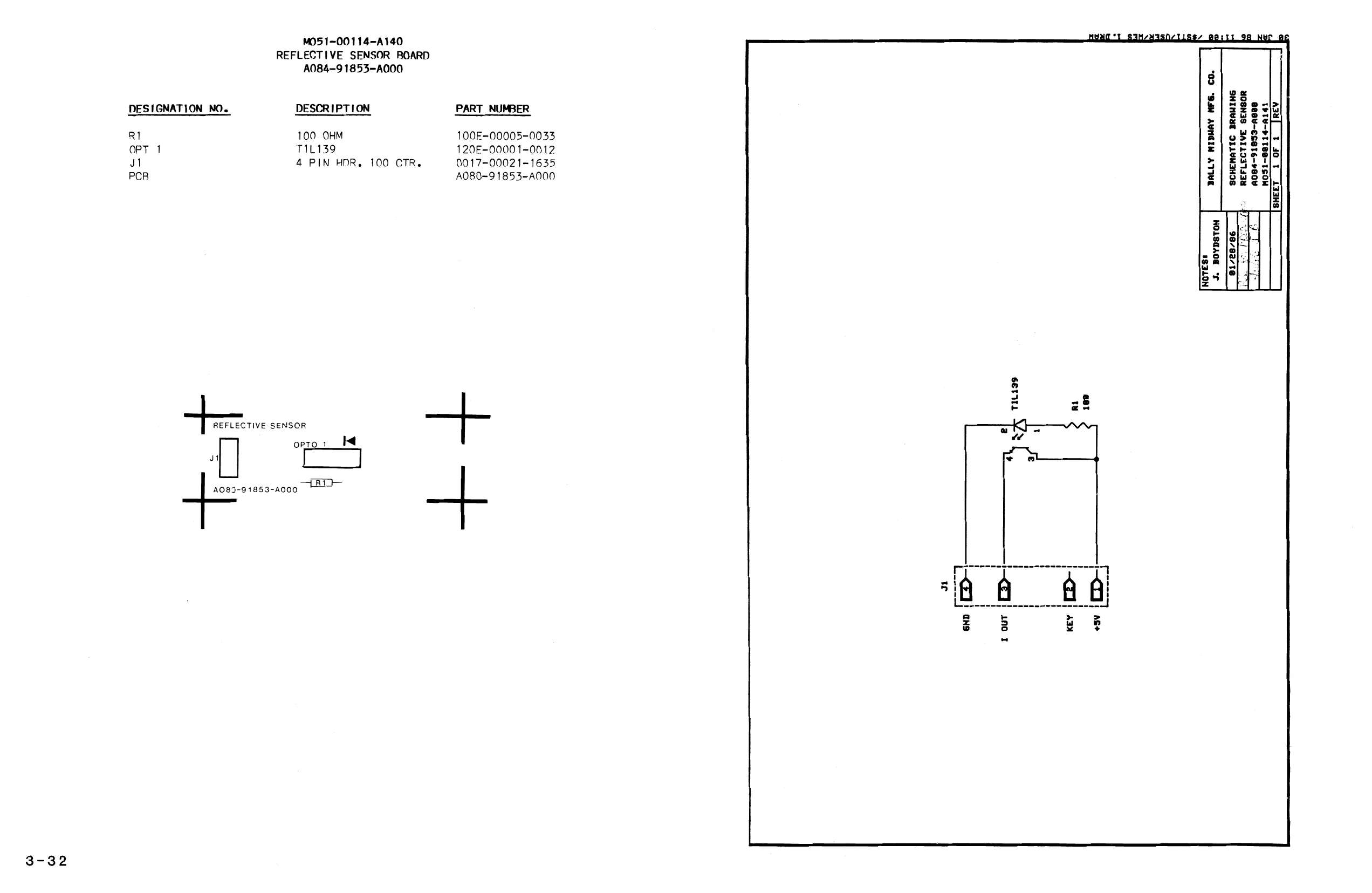
This page is a drawing, shown as the original scan.
LO MONITOR poy
POHER CHASSIS A945-eae59-9260 CONDOR POWER SUPPLY
aRLU-ORN gH
‘@BRN
aGRN
Tlac HoT
~svie Fiev_RTN! Fiavi +12V! tev! SROUND! GROUND! GROUND! GROUND! GROUND! 12 GROUND} 11 GROUND! 12 GROUND!13 WER v_RORK-BUR YO COIN DOCR CuHN
SRCUND | 14 +5v/ 15) +5V1 16 sevli7 +5v/18 s5vit9| +svizol ‘aRED ‘@RED WRED RED
JO SENSOR CONTROL BOARD CI AUDIO ANP BOARD TO SOUND BOARDS
LINE VOLTAGE SELECTION CHART VOLTAGE ) 105) 115 zie; 220 230 | 240 JuNPER if 6-8 | 5-11] 8-14] i1-14 ii-i4{ii-14 JUMPER @[14-15] 14-15] ouT | oUT, our | our BALLAST Jumper 3! 4-7 | 4-10! 4-7 14-7 4-10 4-49 TO MONG BOARD JS
FLOURESCENT LIGHT MONITOR
STRAND
T}erounp GROUND.
GROUND wYEL TO CONTROL CON!
70 SENSOR CONTROL BD.
TO 7. . RESETS, STATUSE!
" sRouna {GROUND
iRESET_OUT {RESET_OUT [etey js5v 1@}GROUND 11} GROUND 6808 VIDEO GAME BOARD ‘TeRounD A884~-91971-DB00 {GROUND j+5v j+sv ikey iReset_ouT |} ROUND, ietev lesv +5 GROUND 2}GROUND
mat 1 T1p4e GROUND! 1¢|
GRY-RED_ gp GRY-BLU DATA @ BLU-RED DATA _3__BLU-ORN
TO POWER CHassis
elvernow slnernc~ CONTROL CONN. STROBE BLU > To coin poor conn. WHT-BRN Fiat vet,
KEYI19 METER_RET!20| METERI21 i GROUND! 22, GROUND |22.
J0_ MONITOR ren{i GROUND! 2 GREENIS| GROUND!4 BLUE!5 Groun!é Kev!?| HBLNK~i8 YBLNK~|9|
rpeel ij 1Pai! 1Pe2! 1P23! 1Pe4! 1Pes! 1Pe6! 1P27! GROUND! we10| 8 Seinen — nats rpi2{i2ppORN-BLU bata pis} tafe ORe=veL Bara KEY 114 IP14115 IP15116 IP16117 1P17118 WAT-VIo TO S.G. SOUND _BOARD HHT-ORN i GRN-BLK YEL-BLK STATUS! SERVICE,
TO TEST BRACKET
TO SOUND BOARDS
REV. 1 374787 PG 3 DS WOTES? BALLY MIDHAY MFG. CO. R. A. PLOUSSARD FEB 17 1987 SPY HUNTER 2 = 18ANG 300 a = 18AG 6eav CABINET WIRING @51-09875-A903
SHEET 1 OF 3 [REV 1
TO_POWER SUPPLY
TURBO CreAP SOUE AK naes-91799-BaRe 33 Ta GROUND VOL POT WIPERTI GROUND aupio outie lsv auDIo ouT!3 ie5y fA GROUND !4 isiev @ GROUND!S isiav AUDIO OUTI6 IE GROUND auplo ouTi7 KEY 8 GROUNDIe IRESET KEY!9 yen |PLOLRESET gy VOL POT alta jE att GROUND @ a Grounp!tt TO POWER SUPPLY Fyvol POT Bi12 Re FL2V_RTN WGRY
DUAL POHER ANP H/MIXER| Ji A084-91648-Ba00 Tle SHIELD Jel Le AUDIO Rel Li AUDIO R-l2ih Li SHIELD KEY! 9H! STRAND GAT
IS 1KEY Lel4 CLR CLR SPEAKER HT. #GRN sTaTUSé TO 68008 BOARD 34 GROUND ¥*YEL ARED i IV @UDIO RETURN NCIS! 1 — = ire SHIELD L- tele iR2 AUDIO 1R1 AUDIO TO 68808 BOARD J3 SPEAKER
‘STRAND +ieV KORN | sir SHIELD a1]v aupro
SOUNDS GOOD BOARD f@e4-91963-B000 ie) VoL POT UIFERIT AUDIO OUTI2 TOSE000 BOARD JE GRN-BLK auaro out!s GROUND YEL=BLK GROUND! 4 TO 8068 BOARD JS ® GROUND!S AUDIO OUTIE GROUND YEL-BLU H AUDIO oUTI7 A GROUND!s TO 88000 BOARD JE uHT-BLK KEY!9 VoL Pot alte A GROUND! 11 WHT-ORN
BLU-GRY
To 68908 BOARD J4
<=} noTEs* BALLY MIDWAY MFG. CO. To 68002 BOARD Je LoussaRD [repay toe] spv wunter CABINET HIRING Nes1-20875-Ae03 AUG 3004
SHEET 2 OF 3 [REV 1
TO_g8000 BOARD J3 LF fyi |erounn HATRED we WHT=BLU pop WHT=BLE ne WHT=GRN i BRN-RED \aDD 2 tuRite BRN-YEL IREAD {GROUND 18 y+sv Lifssy 1BIKEY 131DATA s4jnera 15 i DATA ORH-ERN 161DATA i7!DATA ORH-HHT I ORN-BLK teipaTa 19}Dara 2a}paTA TOPOWER SUPPLY
TO 68008 BOARD JE
TO POWER SUPPLY REFLECTIVE SENSOR CONTROL ABe4-91854-B000
GROUND !i GROUND !2 GRN-RED +5V1 18 +5V1 aL An 21s IN 116 is KEV/9 Dt GRN-WHT IN 413 TF cRN-VEL IN 314 ‘@ROUNDIZ GROUND Ie +5vi12] +5V{ 13] GRN-RED
TO 15 Pos M-H-L p-SRN-HHT
a
TO 15 POS M-N-L REFLECTIVE SENSOR A@84-91953-AI00 T]GRouND
REFLECTIVE SENSOR a084-91853-Ae08 gi |cRounp 2}ouT istkey Be} +59
REFLECTIVE SENSOR jaae4-91853-aeeo
REFLECTIVE SENSOR Ave4~91853-A000) T}eRounp 2tour is 1KEY 41 35y
18 POS H-N-L To 68@00 BOARD 4
COIN DOOR LIGHTS C COIN DOOR ORN~BLK C 9 SRYCR
COIN METER 1 HHT VEL, oR Coie sense nosey v9
TO 68098 BOARD Je Lp yp pex-ren ‘ af BLK-BLU af BERYL BLK-GRN
or ef SRY BLY 7p SRE op SRY-ERN
TO REFLECTIVE SENSOR CONTROL BOARD Ji JO.s290 B0ARD 33
TO_68008 BOARD J2 GRN ROA GEAR
WHT @ R 2 GEAR SEAR 4 ORN 0 + R 9. GEAR SEAR +4 GEAR BRN e —o L GEAR
GEAR BLK 4 GEAR
SEAR GRY +
- GEAR
START BLU-BLK o ° + START
START BLU-WHT. START e
an i
GROUND YEL-GRN als |
cr}
TO 68008 BOARD J3 t
RMISSLE GRY-RED R NYSSLE 0 CL. TRIGGER) R QIL H
R OIL ek GRY-BLU
<b. THUMBD R’ GUN ° KR. TRIGGER? R_GUN | at GRY-YEL ae R SLASHER L___GRY-GRN R SLASHER
GROUND —#cR. THUNED
_MISSLE: BLK-RED L wgSsLe
LOL BLK-BLU (L. TRIGGER? © L git “fee. rau»
L_GUN BLK-YEL
\_ SLASHER BLK-GRN L gUN —o <R. TRIGGER) L SLASHER
GROUND. YEL-RED
pie 0 <R, THUMB?
TO REFLECTIVE SENSOR
REV. 1 3¢4787 SHOW 15-POS CONNECTOR TO 6K BOARD AND ADD NEW BUTTON NAMES. DS
NOTES®
R. A, PLOUSSARD BALLY MIDWAY MFG. CO.
FEB 17 1987 SPY HUNTER 2
M@51-00875-Aee3
SHEET 3 OF 3 [REV 1
3-35