Lunar Lander DP-136-2nd-01B
Lunar Lander (rev 2) (Atari, 1979) · Drawing Package · 1 pages · original scan
POWER INPUT
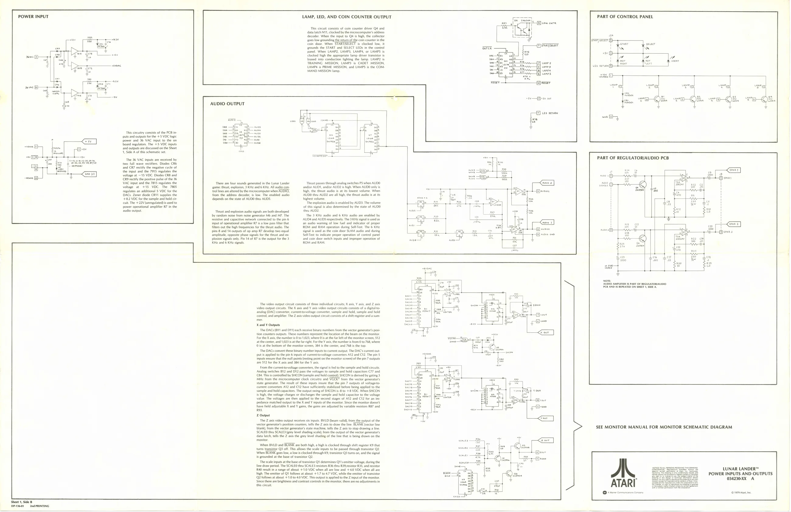
This circuitry consists ofthe PCB inputs and outputs forthe +5 VDC log power and 36 VAC input to the on board regulators. The +5 VOC inputs and outputs are discussed on the Sheet 1, Side A of ths schematic set. ‘The 36 VAC inputs are received by ‘wo full wave rectties. Diodes CRE and CR7 rectify the negative cycle of the input and the 7915 regulates the voltage at ~15 VOC. Diodes CRB and
CR9 rectify the positive pulse ofthe 36
VAC input and the 7815 regulates the voltage at +15 VDC. The 7805 regulates an additional 5 VDC for the DACs. Zener diode CRIT supplies the +82 VDC forthe sample and hold cir ‘uit. The +22V (unregulated) is used to ower operational amplifier R7 in the audio output. LAMP, LED, AND COIN COUNTER OUTPUT
This circuit consists of coin counter driver Q& and
data latch N11, clocked by the microcomputer’ address
‘decoder. When the input to QS is high, the collector
00s low grounding the return of the coin counter in the
Coin door. When STARTISELECT is clocked low, it grounds the START and SELECT LEDs in the control panel. When LAMP2, LAMP3, LAMPS, or LAMPS is clocked high the appropriate lamp diver transistor is biased into conduction lighting the lamp. LAMP2 is TRAINING MISSION, LAMPS. is CADET MISSION, LAMPS is PRIME MISSION, and LAMPS is the COM: MAND MISSION lamp,
‘Sheet 1, Side B P3601 2nd PRINTING AUDIO OUTPUT ieraprreee d i (LES tea
sr
Ez] tane 2 canes a] anes fe] canes
sv —Hsr ov
Leo aero
There are four sounds generated in the Lunar Lander ‘game: thrust, explosion, 3 KHz and 6 KHz. All audio con-
‘uo lines are altered by the microcomputer when AUDIO,
from the address decoder, is low. The enabled audio {depends on the state of AUDO thru AUDS, ‘Thus passes through analog switches P5 when AUDO andlor AUDI, andlor AUD? is high. When AUDO only is high, the thrust audio is at its lowest volume. When ‘AUDO thru AUD2 are all igh, the thrust audio i at its highest volume. The explosion audio is enabled by AUD3. The volume ofthis signal is also determined by the state of AUDO thew AUD2, The 3 KHz audio and 6 KHz audio are enabled by ‘AUD4 and AUDS respectively. The 3 KHz signals used as fan audio warning of low fuel and indicator of proper ROM and RAM operation during SeltTest. The 6 KHz signal is used as the coin door SLAM audio and during Self-Test to indicate proper operation of control panel and coin door switch inputs and improper operation of ROM and RAM. ‘Thrust and explosion audio signals are both developed by random noise from noise generator M6 and M7. The resistive and capacitive network connected to the pin 6 input of operational amplifier R7 is a low pass filter that filters out the high frequencies forthe thrust audio. The pins 8 and 14 outputs of op amp R7 develop two equal amplitude, opposite phase signals forthe thrust and ex: plosion signals only. Pin 14 of R7 isthe output forthe 3 KHz and 6 KHz signals. jl Gravee
‘The video output citcuit consists of three individual circuits; X axis, ¥ axis, and Z axis video output cicuis. The X axis and Y axis video output circuits consists of a digitaltoanalog (DAC) converter, currentto-voltage converter, sample and hold, sample and hold Control, and amplifier. The Z axis video output circuit consists ofa shift register anda sum
Xand Y Outputs The DACS (B11 and D11) each receive binary numbers from the vector generator’s posi tion counters outputs. These numbers represent the location ofthe beam on the monitor. For the X axis, the number i0 to 1023, where Os atthe far left ofthe monitor screen, 512, atthe center, and 1,023 i atthe far right. For the Y axis, the number is from 0 t0 768, where 0 is at the bottom of the monitor screen, 384 isthe center, and 768 isthe top. The DACs convert these binary number inputs to current output. The DAC’s curent out ‘put i applied to the pin 6 inputs of currenttovoltage converters A12 and C12. The pin 5 Inputs ensue thatthe null points resting point on the monitor screen) ofthe pin 7 outputs are 512 forthe X axis and 384 for the ¥ axis. From the currentto-voltage converters, the signal i fed tothe sample and hold circuit, ‘Analog switches B12 and D12 pass the voltages to sample and hold capacitors C77 and (CB4, This is controlled by SHCON (sample and hold control) SHCON is derived by gating 3 MHz from the microcomputer clock circuitry and VGCK" from the vector generators state generator. The result of these inputs insure that the pin 7 outputs of voltagetocurrent converters A12 and C12 have sufficiently stabilized before being applied to the sample and hold capacitors. The output swing of SHCON is 8 to +8 VDC. When SHCON 's high, the voltage charges or discharges the sample and hold capacitor to the voltage value. The voltages are then applied to the second stages of ATZ and C12 for an imppedance matched output to the X and Y inputs of the monitor. Since the monitor doesnt hhave field adjustable X and Y gains, the gains ae adjusted by variable resistors R87 and R93. Z Output ‘The Z axis video output receives six inputs. BVLD (beam valid, from the output of the vector generators position counters, tells the Z axis to draw the line. BLANK (vector line bank) from the vector generator’ state machine, tells the Z axis to stop drawing a line. SSCALEO thru SCALES (grey level shading scale} from the output ofthe vector generators data latch, tells the Z axis the grey level shading of the line that is being drawn on the monitor. When BVLO and BTANK are both high, a high is clocked through shift register K9 that tums transistor Q3 off. This allows the scale inputs to be passed theough transistor Q2. When BLANK goes low, a low is clocked through K9, transistor Q3 turns on, and the signal Is grounded at the base of transistor Q2 The scale inputs at the base of transistor Q1 determines Q's emitter voltage, during the line draw period. The SCALEO thru SCALES resistors R36 thru R39,esistor R35, and resistor R40 result in a range of about +1.0 VDC when all ate low and -+40 VDC when al are high. The emitter of Q1 follows at about +1,7 to 47 VOC, while the emitter of transistor Q2 follows at about +1.0 to 40 VOC. This output is applied tothe Z input ofthe monitor. Since there are brightness and contrast controls inthe monitor, there are no adjustments in this circuit, aT “| RT OF CONTROL PANEL
seams
ww
Lee neroen
oo Gr
PART OF REGULATORIAUDIO PCB
= |A0bIO AMPurice is ar oF REGULATORALDIO EO AND IS RUPEATEO ON SHEET 1 S1DU 8
SEE MONITOR MANUAL FOR MONITOR SCHEMATIC DIAGRAM
LUNAR LANDER™ skewer © POWER INPUTS AND OUTPUTS ATARI eed 034230-XX A
©1979 Kar Ine