Kangaroo SP-204 2nd Printing
Kangaroo (Sun Electronics, 1982) · Schematic Package · 23 pages · 54 sections · original scan
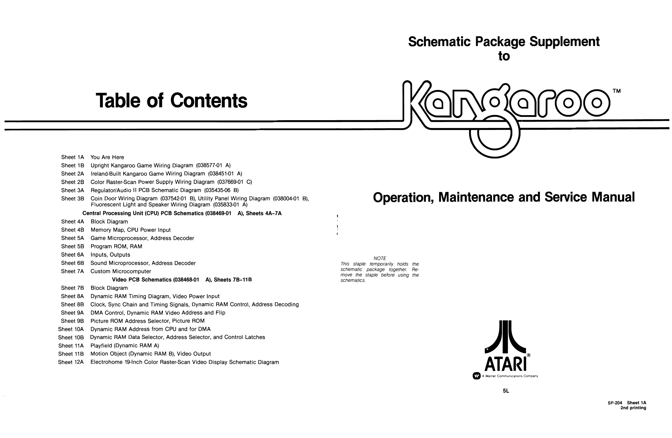
Sheet 1A Sheet 1B Sheet 2A Sheet 2B
Sheet 3A Sheet 3B Schematic Package Supplement to
Table of Contents
You Are Here Upright Kangaroo Game Wiring Diagram (038577-01 A) lreland-Built Kangaroo Game Wiring Diagram (038451-01 A) Color Raster-Scan Power Supply Wiring Diagram (037669-01 C) Regulator/Audio 11 PCB Schematic Diagram (035435-06 B) Coin Door Wiring Diagram (037542-01 B), Utility Panel Wiring Diagram (038004-01 B), Operation, Maintenance and Service Manual Fluorescent Light and Speaker Wiring Diagram (035833-01 A) Central Processing Unit (CPU) PCB Schematics (038469-01 A), Sheets 4A-7A ; Sheet 4A Sheet 4B Sheet 5A Sheet 5B
Sheet 6A Sheet 6B Sheet 7A
Sheet 7B
Sheet 8A Sheet 8B Sheet 9A Sheet 9B Sheet 10A
Sheet 10B Sheet 11A Sheet 11B Sheet 12A Block Diagram Memory Map, CPU Power Input Game Microprocessor, Address Decoder Program ROM, RAM Inputs, Outputs NOTE Sound Microprocessor, Address Decoder This staple temporarily holds the Custom Microcomputer schematic package together. Re- ‘4 | move the staple before using the Video PCB Schematics (038468-01 A), Sheets 7B-11B schematics. Block Diagram Dynamic RAM Timing Diagram, Video Power Input Clock, Sync Chain and Timing Signals, Dynamic RAM Control, Address Decoding DMA Control, Dynamic RAM Video Address and Flip Picture ROM Address Selector, Picture ROM Dynamic RAM Address from CPU and for DMA Dynamic RAM Data Selector, Address Selector, and Control Latches Playfield (Dynamic RAM A) Motion Object (Dynamic RAM B), Video Output ® Electrohome 19-Inch Color Raster-Scan Video Display Schematic Diagram ATARI
SL
SP-204 Sheet 1A
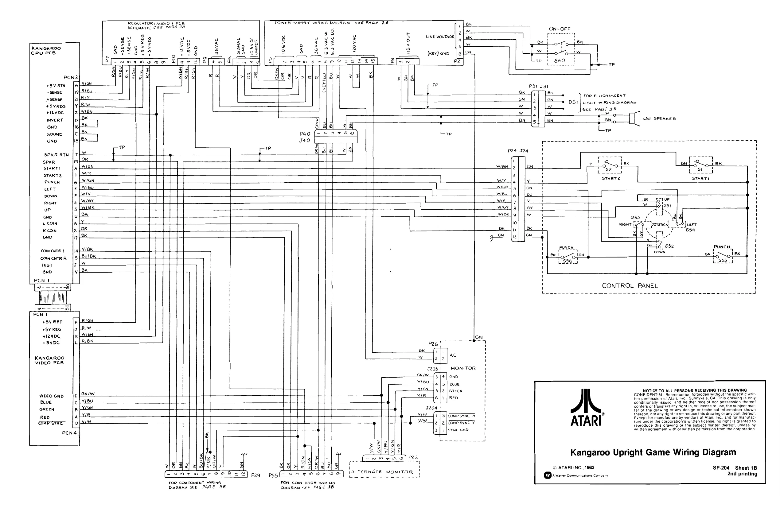
This page is a drawing, shown as the original scan.
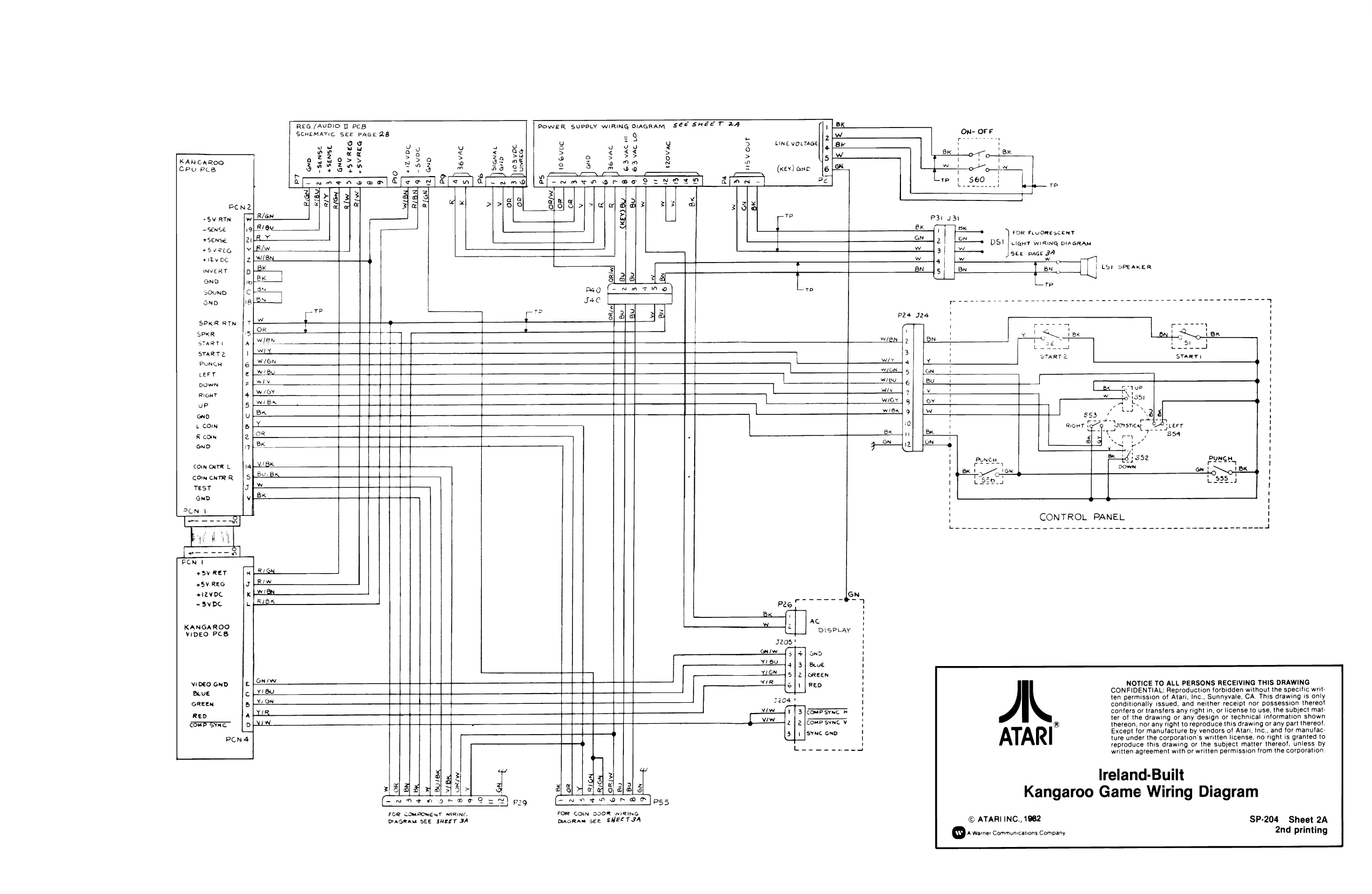
This page is a drawing, shown as the original scan.
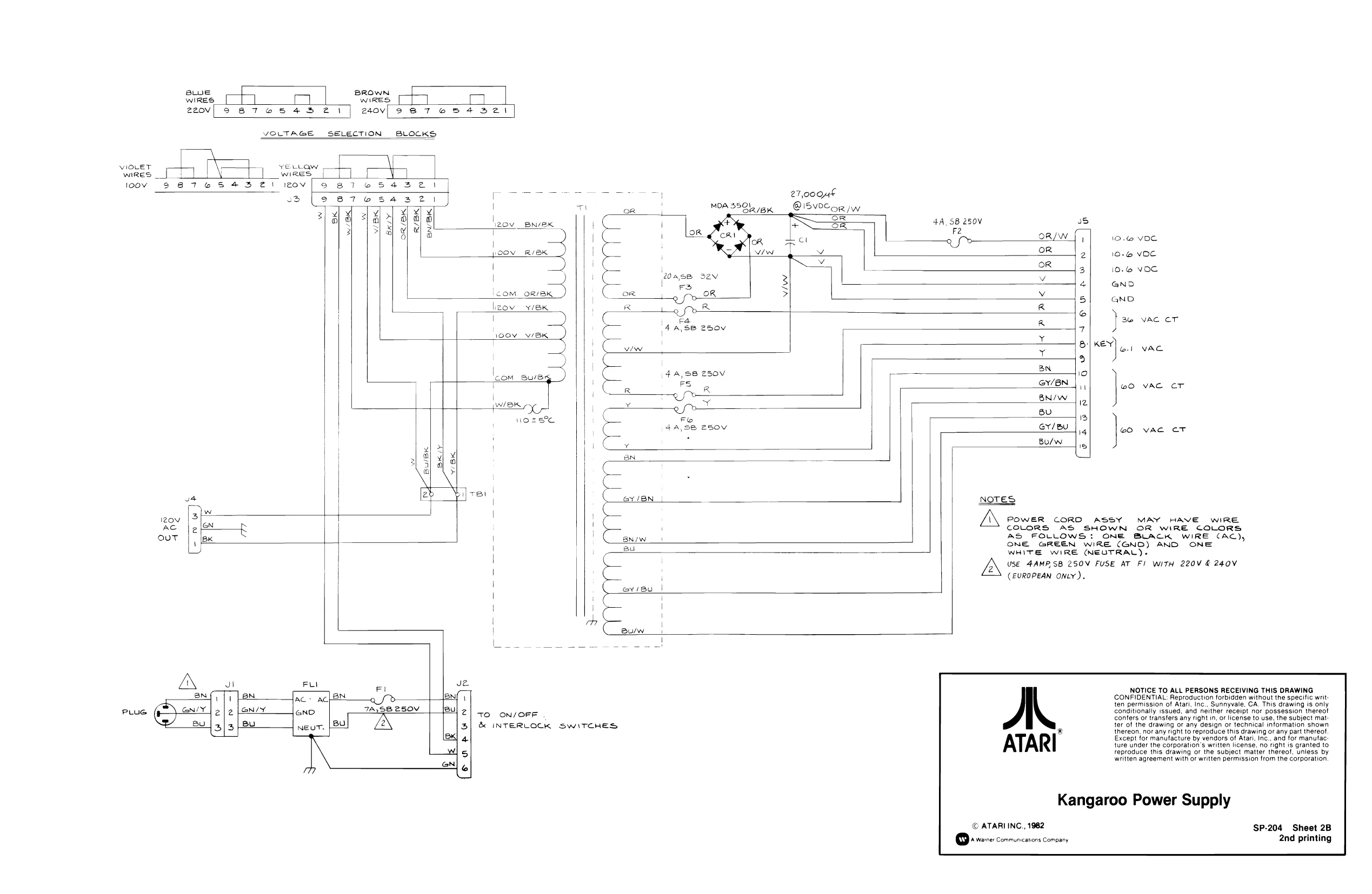
This page is a drawing, shown as the original scan.
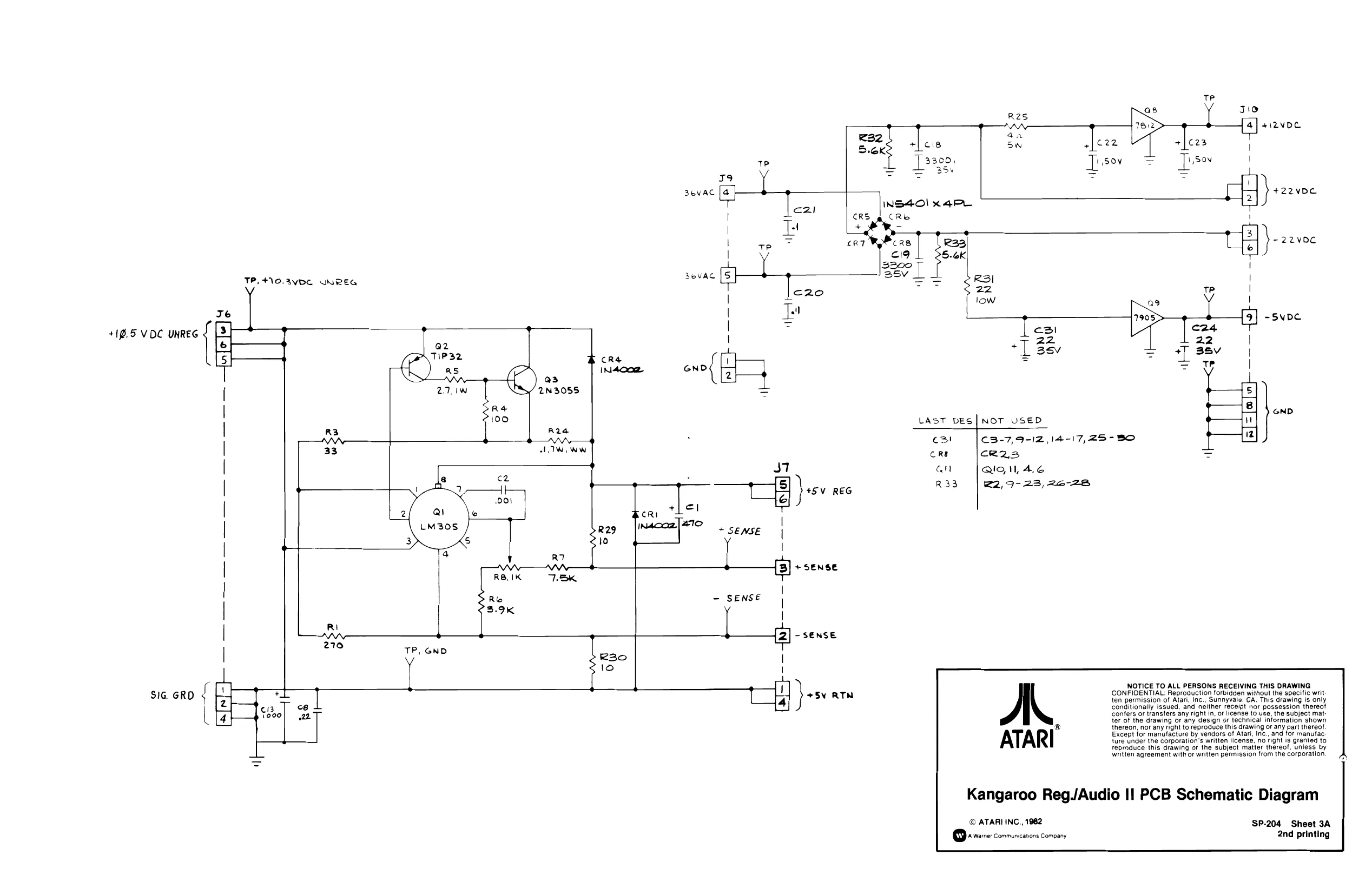
This page is a drawing, shown as the original scan.
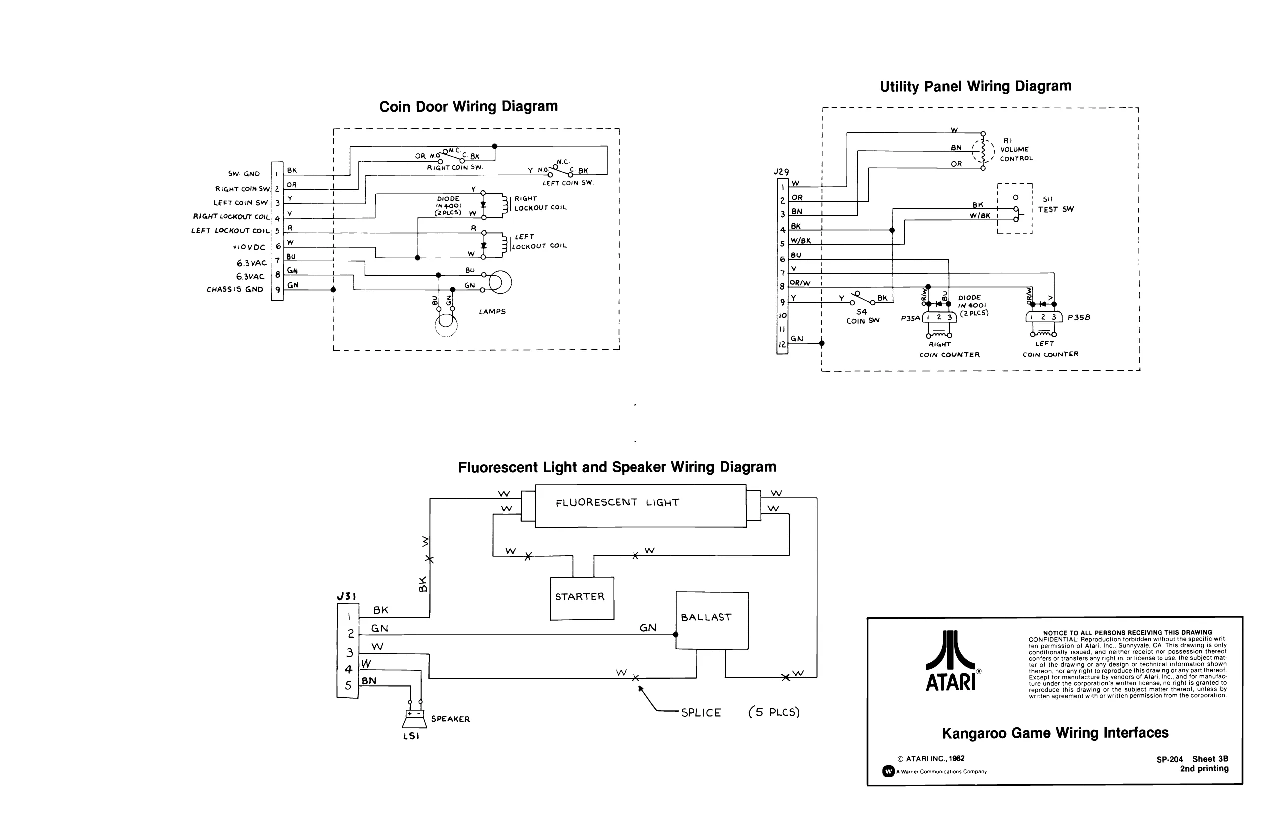
This page is a drawing, shown as the original scan.
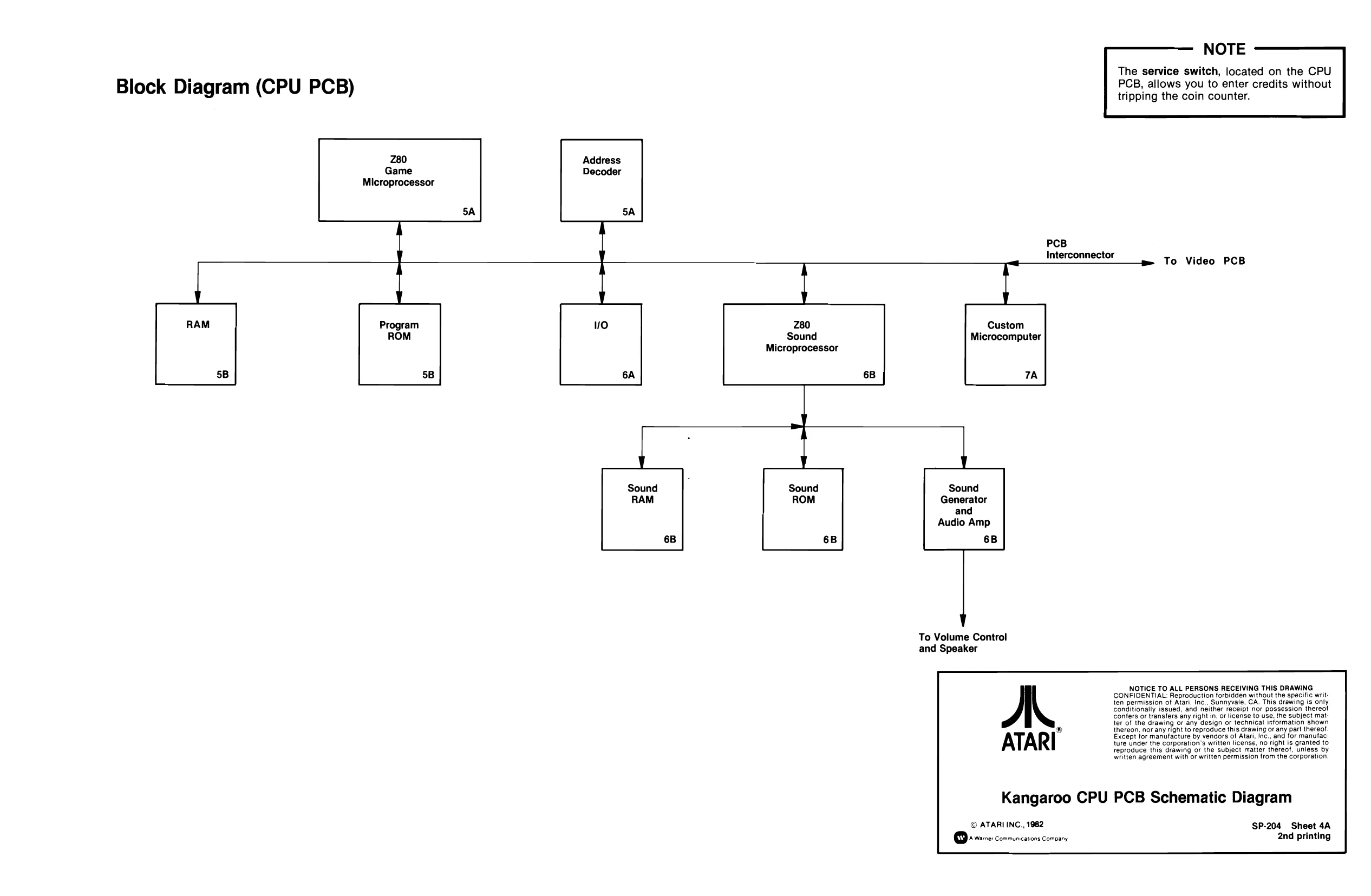
Block Diagram (CPU PCB)
Z80 Game Microprocessor
PCB
NOTE
The service switch, located on the CPU PCB, allows you to enter credits without tripping the coin counter.
Interconnector
Z80 Sound Microprocessor Custom Microcomputer
7A
Sound RAM Sound Generator and Audio Amp
6B
To Volume Control
A
ATARI
To Video PCB
NOTICE TO ALL PERSONS RECEIVING THIS DRAWING CONFIDENTIAL: Reproduction forbidden without the specific writ ten permission of Atari, Inc., Sunnyvale, CA. This drawing is only conditionally issued, and neither receipt nor possession thereof confers or transfers any right in, of license to use, the subject matter of the drawing or any design or technical information shown thereon, nor any right to reproduce this drawing or any part thereof. Except for manufacture by vendors of Atari, Inc., and for manufac: ture under the corporation's written license, no right is granted to reproduce this drawing or the subject matter thereof, unless by written agreement with or written permission from the corporation.
Kangaroo CPU PCB Schematic Diagram
© ATARI INC., 1982
|A Warner Communications Company SP-204 Sheet 4A
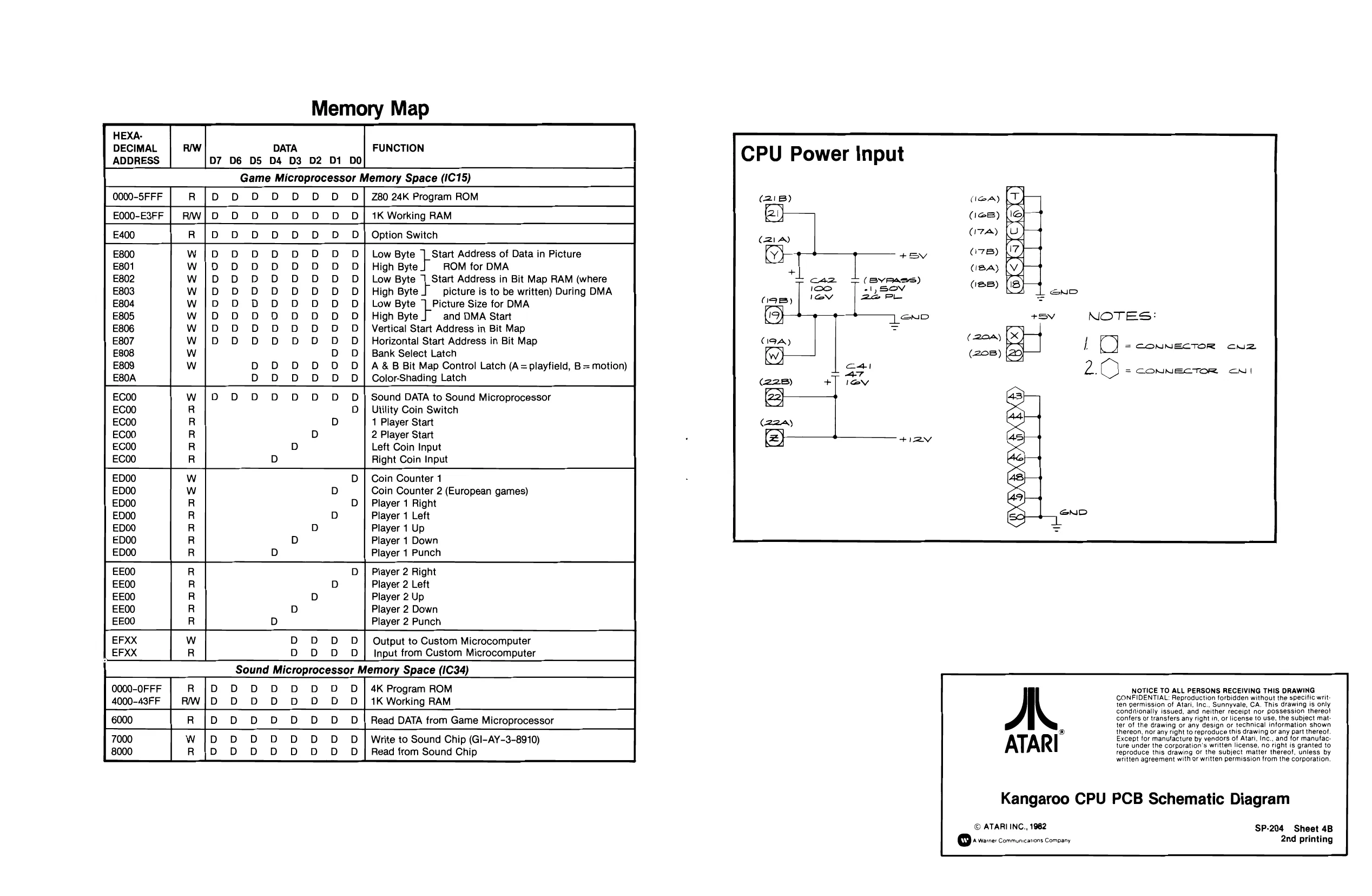
Memory Map
b6 0s 0403 02 D1 DO] CPU Power Input Game Microprocessor Memory Space (IC 15) 280 24K Program ROM (218)
1K Working RAM
Option Switch
Low Byte Start Address of Data in Picture High Byte ROM for DMA Low Byte 1 Start Address in Bit Map RAM (where High Byte picture is to be written) During DMA Low Byte 7] Picture Size for DMA High Byte and DMA Start Vertical Start Address in Bit Map Horizontal Start Address in Bit Map | Bank Select Latch > a.
A & B Bit Map Control Latch (A = playfield, B = motion) Oo =
Color-Shading Latch 2. CONNECTOR oN! 0000-5FFF R £000-E3FF | RW | io} fo} oO vouo000000/oI|0l/o vo000000/0Io cuo00000D/oI|oO cso00000n0/oIo/oO voovo0voco/oC|o CONNECTOR cuz SSSSSSSS=S=E/z o9l00 voV900000|0Io ojo90000000T0D]Nl/o Sound DATA to Sound Microprocessor Utility Coin Switch 1 Player Start 2 Player Start Left Coin Input Right Coin Input
Coin Counter 1 Coin Counter 2 (European games) Player 1 Right Player 1 Left Player 1 Up Player 1 Down Player 1 Punch Player 2 Right Player 2 Left Player 2 Up Player 2 Down Player 2 Punch voljo000000000D/NlN oO
Output to Custom Microcomputer Input from Custom Microcomputer Sound Microprocessor Memory Space (IC34) 0000-OF FF D | 4K Program ROM NOTICE JO ALL PERSONS RECEIVING THIS DRAWING i CONFIDENTIAL: Re duction forbidden without the specific writ: 4000-43FF D | 1K Working RAM fen permission of Atan. Inc. Sunnyvale, CA. This dtawing is only
® w R R R R R
Ww w R R R R R
R R R R R
w R
Conditionally Issued, and neither receipt nor possession thereot
confers or transfers any right in, or license to use, the subject mat
ter of the drawing or any design or technical information shown ® thereon, nor any right to reproduce this drawing or any part thereot Write to Sound Chip (GI-AY-3-8910) ATARI Except for manvfacture by vendors of Atari, Inc., and for manufac: : ture under the corporation's written license, no right is granted to Read from Sound Chip reproduce this drawing or the subject matter thereof, unless by wntten agreement with ar written permission from the corporation Read DATA from Game Microprocessor
Kangaroo CPU PCB Schematic Diagram
© ATARI INC., 1962 SP-204 Sheet 4B + warner Communcanions Company 2nd printing
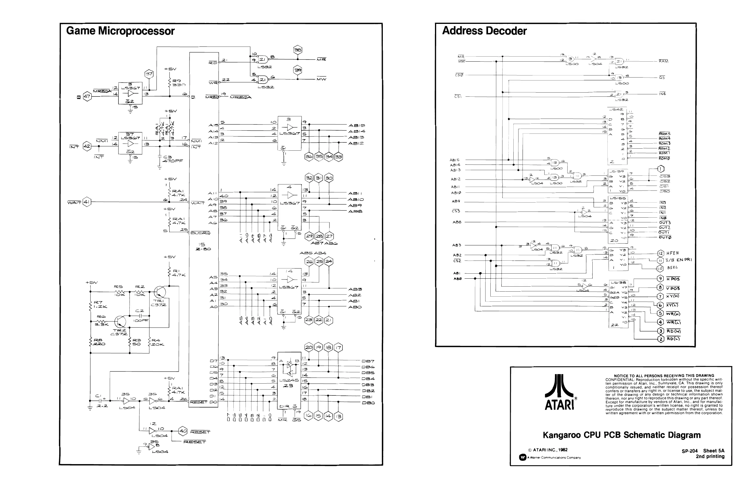
This page is a drawing, shown as the original scan.
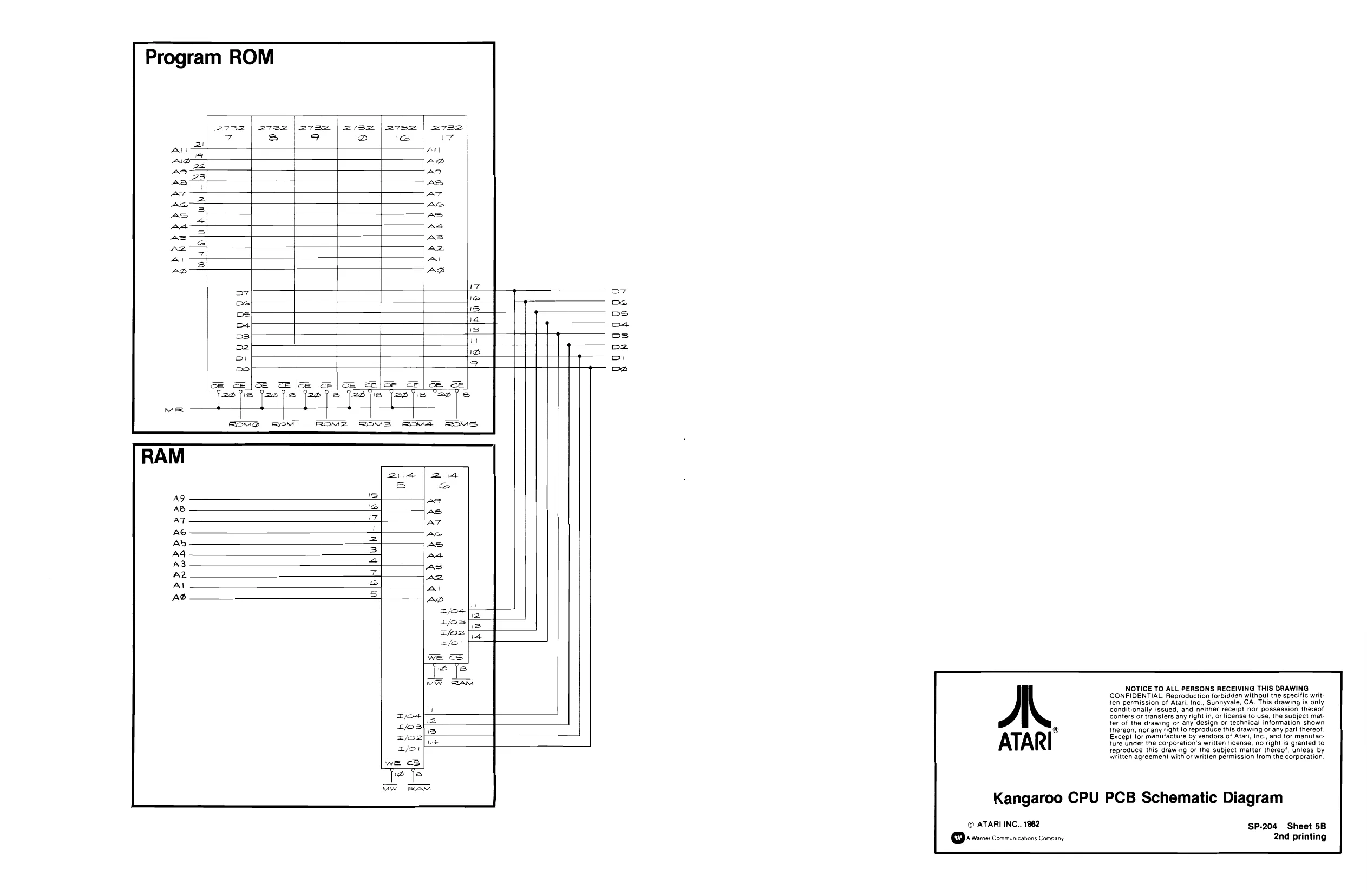
This page is a drawing, shown as the original scan.
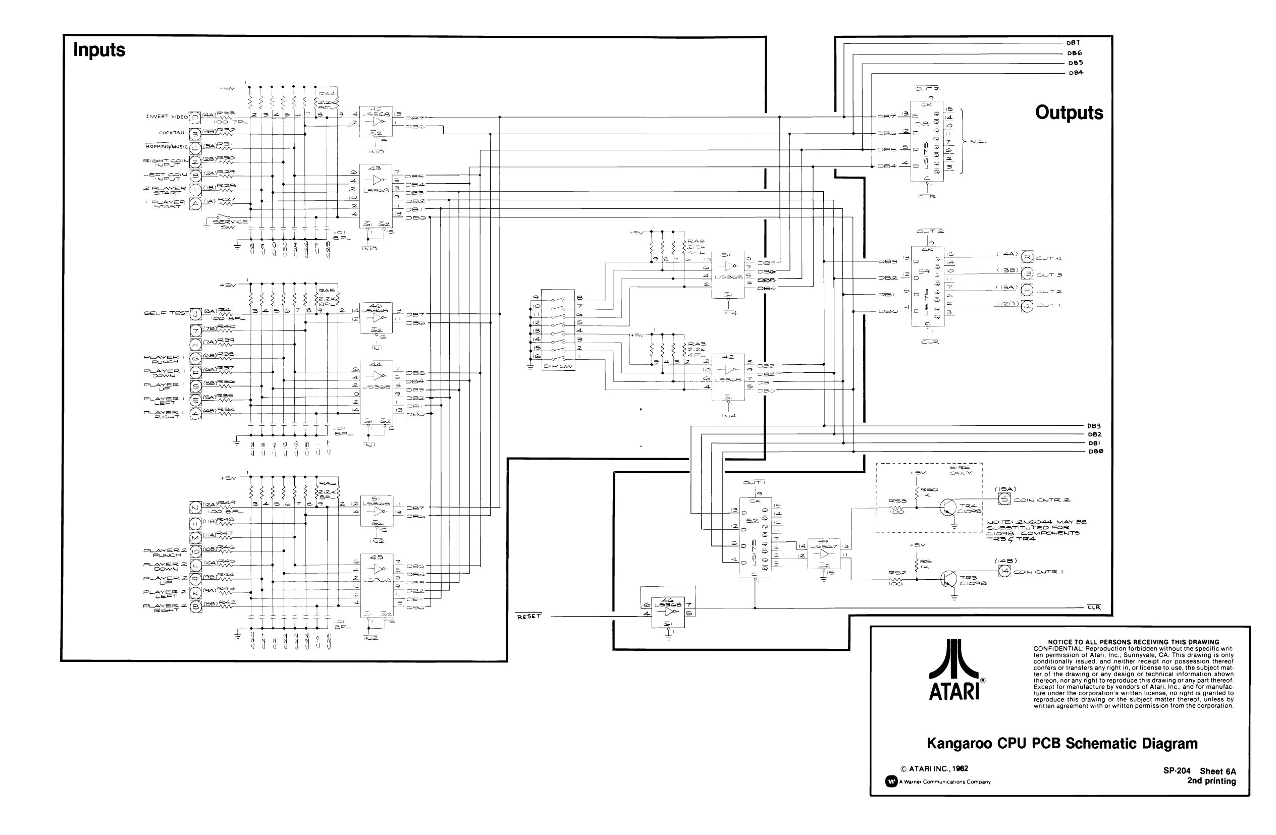
This page is a drawing, shown as the original scan.
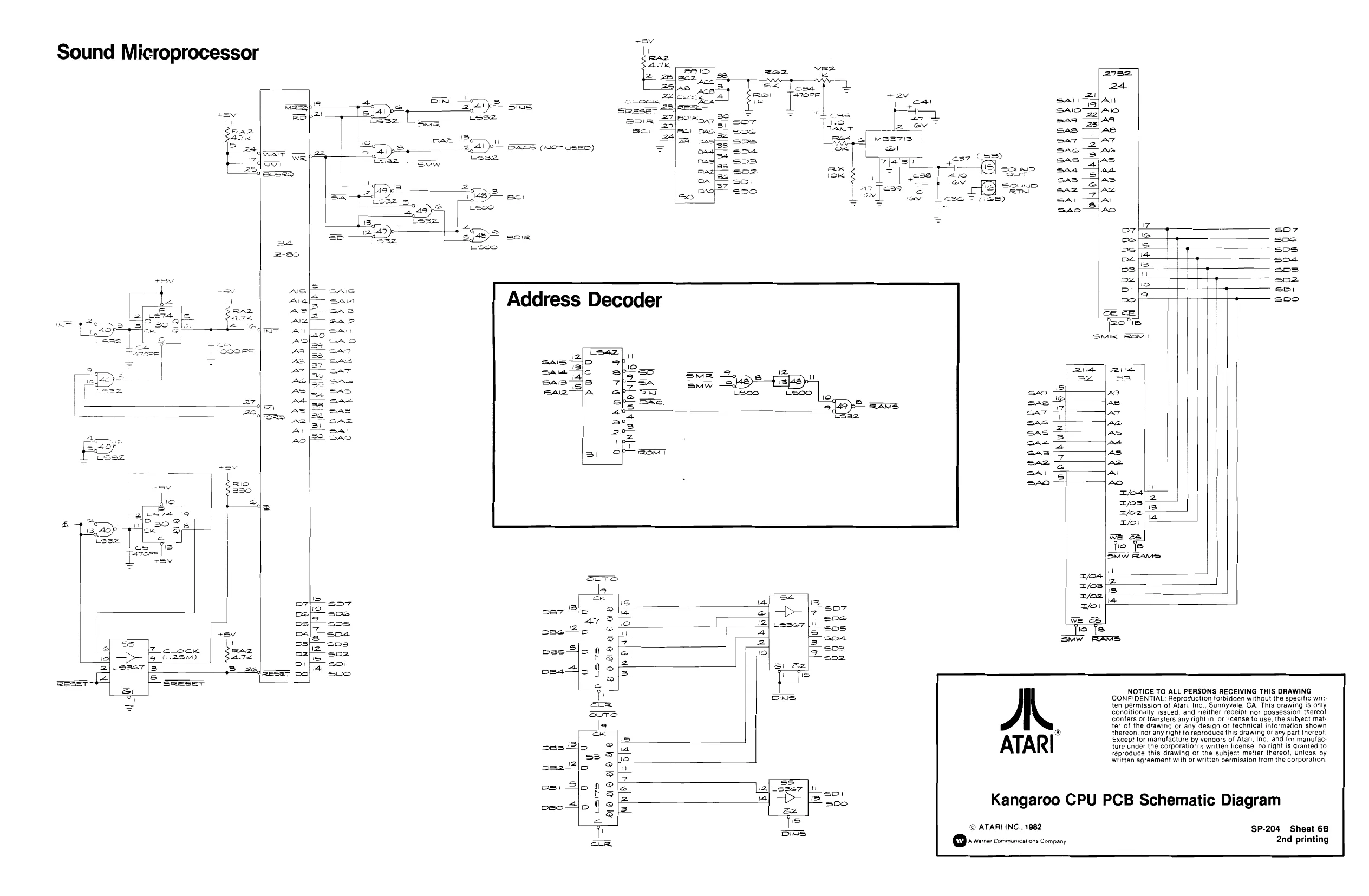
This page is a drawing, shown as the original scan.
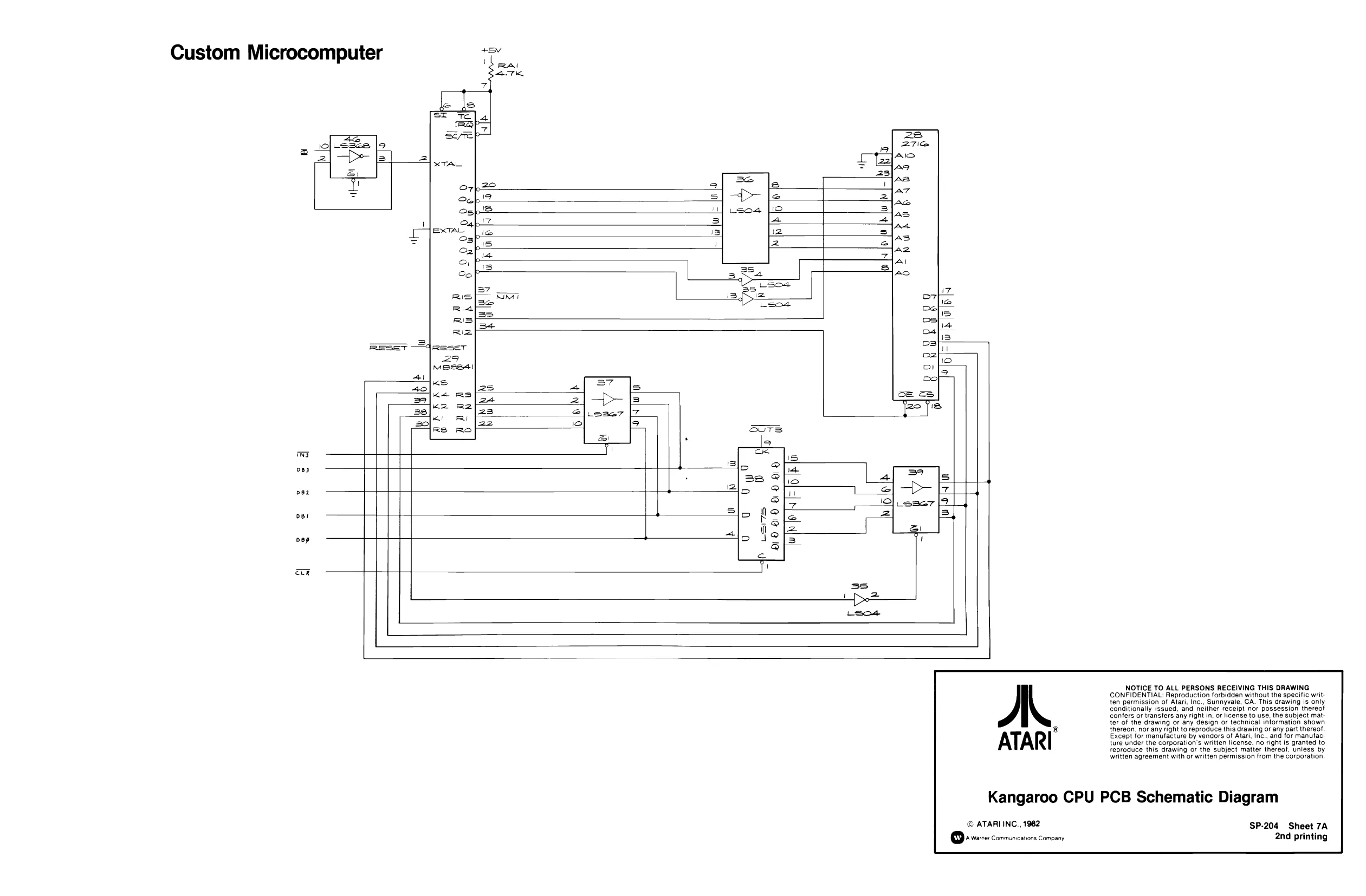
This page is a drawing, shown as the original scan.
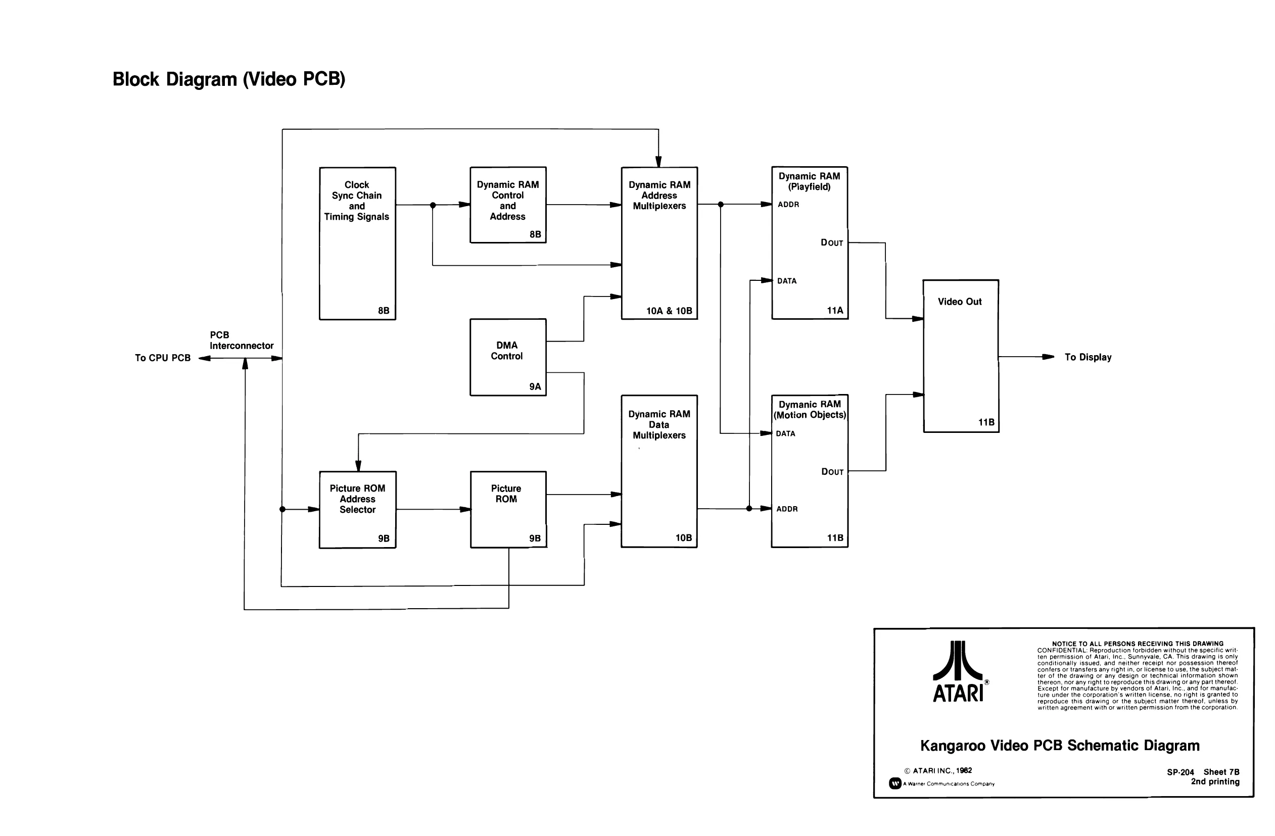
Block Diagram (Video PCB)
PCB Interconnector
To CPU PCB =
Clock Sync Chain and Timing Signals Dynamic RAM Control and Address
8B
DMA Control
Picture ROM Address Selector
9B Dynamic RAM Address Multiplexers
Dynamic RAM Data Multiplexers Dynamic RAM (Playfield)
ADDR
Dymanic RAM Video Out
To Display
NOTICE TO ALL PERSONS RECEIVING THIS DRAWING CONFIDENTIAL: Reproduction forbidden without the specific writ
ten permission of Atari, Inc., Sunnyvale, CA. This drawing is only
conditionally issued, and neither receipt nor possession thereof confers or transfers any right in, or license to use, the subject matter of the drawing or any design or technical information shown ® thereon, nor any right to reproduce this drawing or any part thereof. Except for manufacture by vendors of Atari, Inc., and for manufac: ture under the corporation's written license, no right is granted to reproduce this drawing or the subject matter thereof. unless by written agreement with or written permission trom the corporation.
Kangaroo Video PCB Schematic Diagram
© ATARIINC., 1962 SP-204 Sheet 7B QD A Warne: Communcanions Comoany 2nd printing
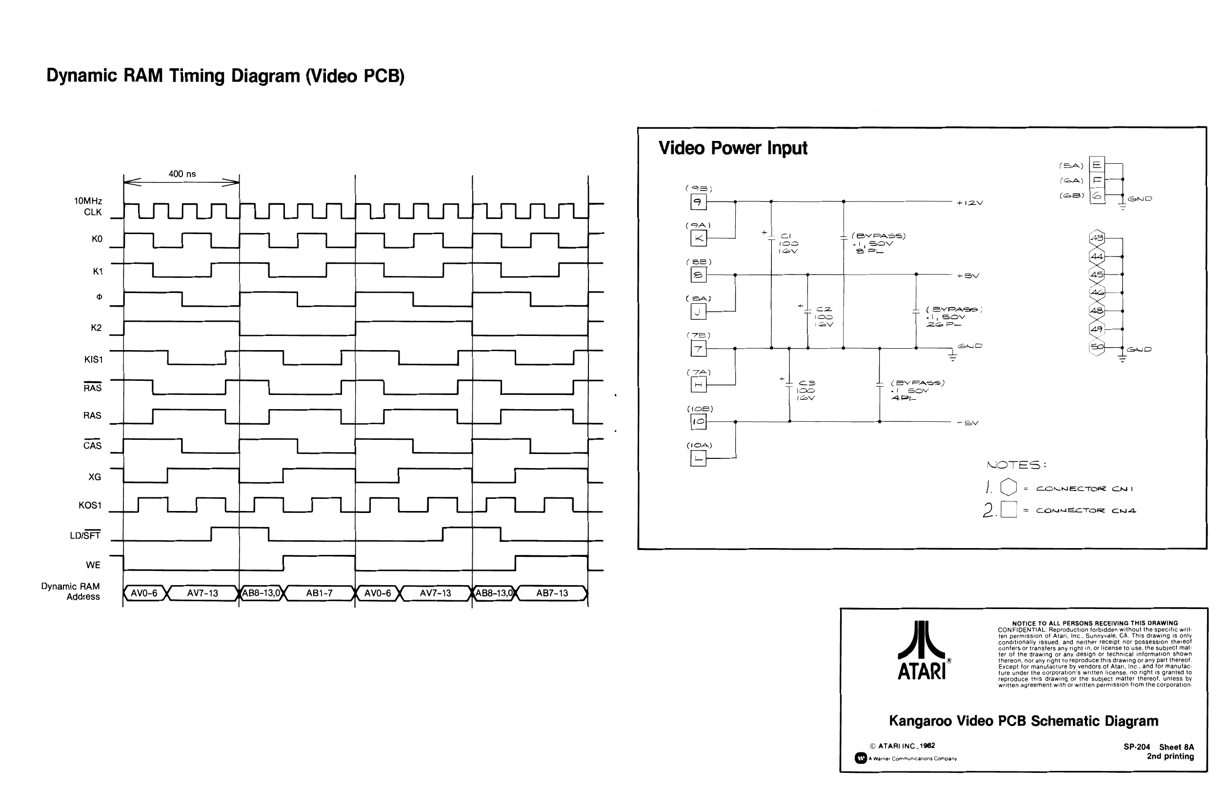
Dynamic RAM Timing Diagram (Video PCB)
1OMHz CLK
KO
Kt
K2
KIS1
RAS
RAS
CAS
XG
Kosi
LoiSFT
WE
Dynamic RAM Address 400 ns
Video Power Input
NOTES:
CONNECTOR CNI
CONNECTOR CN
NOTICE TO ALL PERSONS RECEIVING THIS DRAWING
CONFIDENTIAL: Reproduction forbidden without the specific writ ‘confers or transfers any right in, or license to use, the subject mat:
ten permission of Atari, Inc., Sunnyvale, CA. This drawing is only conditionally issued, and neither receipt nor possession thereof
ter of the drawing or any design or technical information shown
® thereon, nor any right to reproduce this drawing or any part thereof,
Except for manufacture by vendors of Atari, Inc., and for manufac: ture under the corporation's written license, no right is granted to reproduce this drawing or the subject matter thereof, unless by written agreement with or written permission from the corporation.
Kangaroo Video PCB Schematic Diagram
© ATARI INC.,1982 SP-204 Sheet 8A reine: communicanons Company 2nd printing
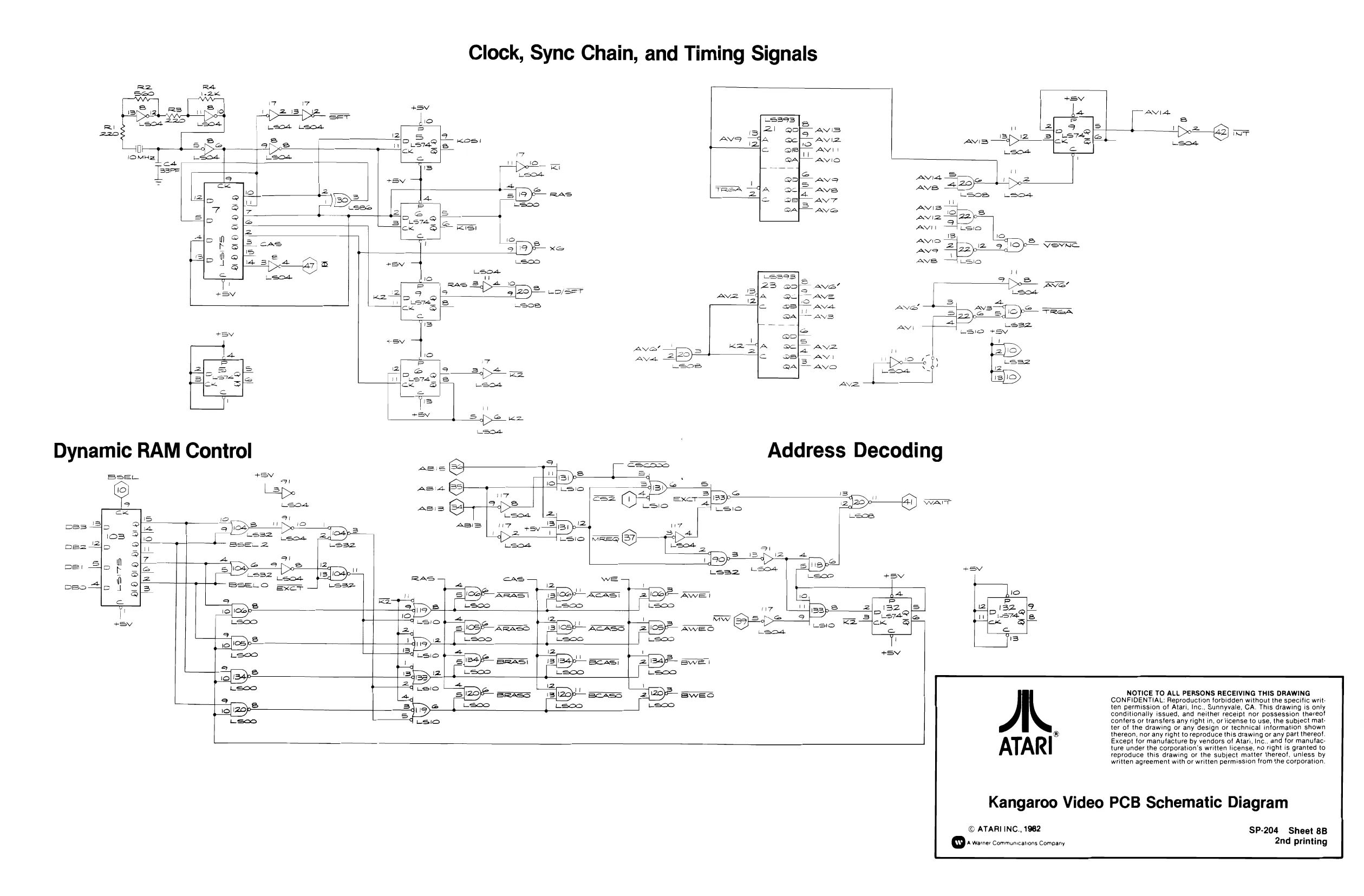
This page is a drawing, shown as the original scan.
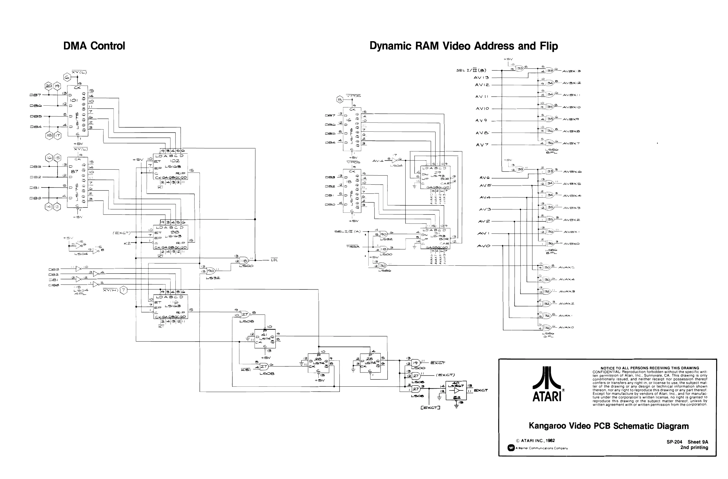
This page is a drawing, shown as the original scan.
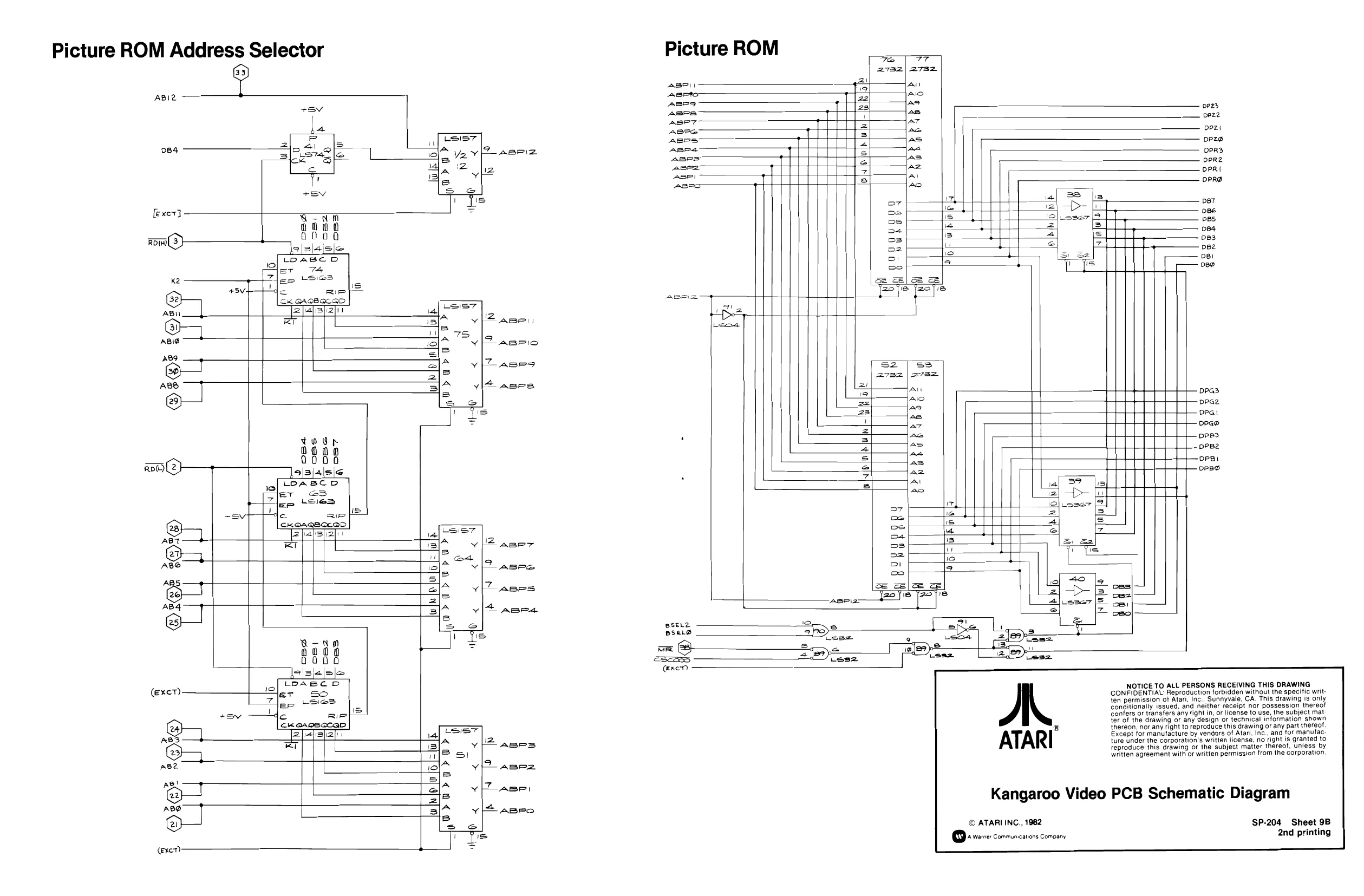
This page is a drawing, shown as the original scan.
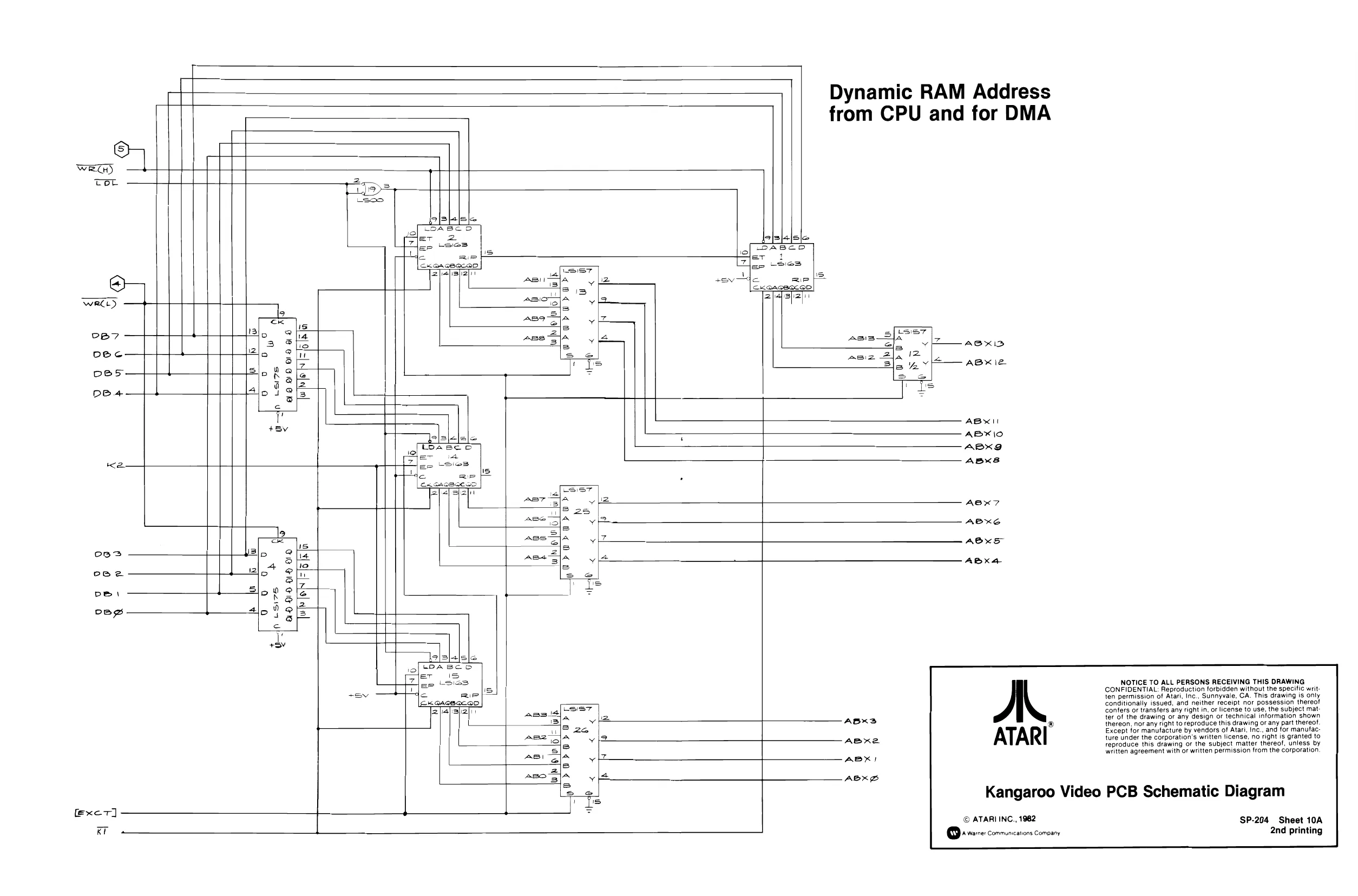
This page is a drawing, shown as the original scan.
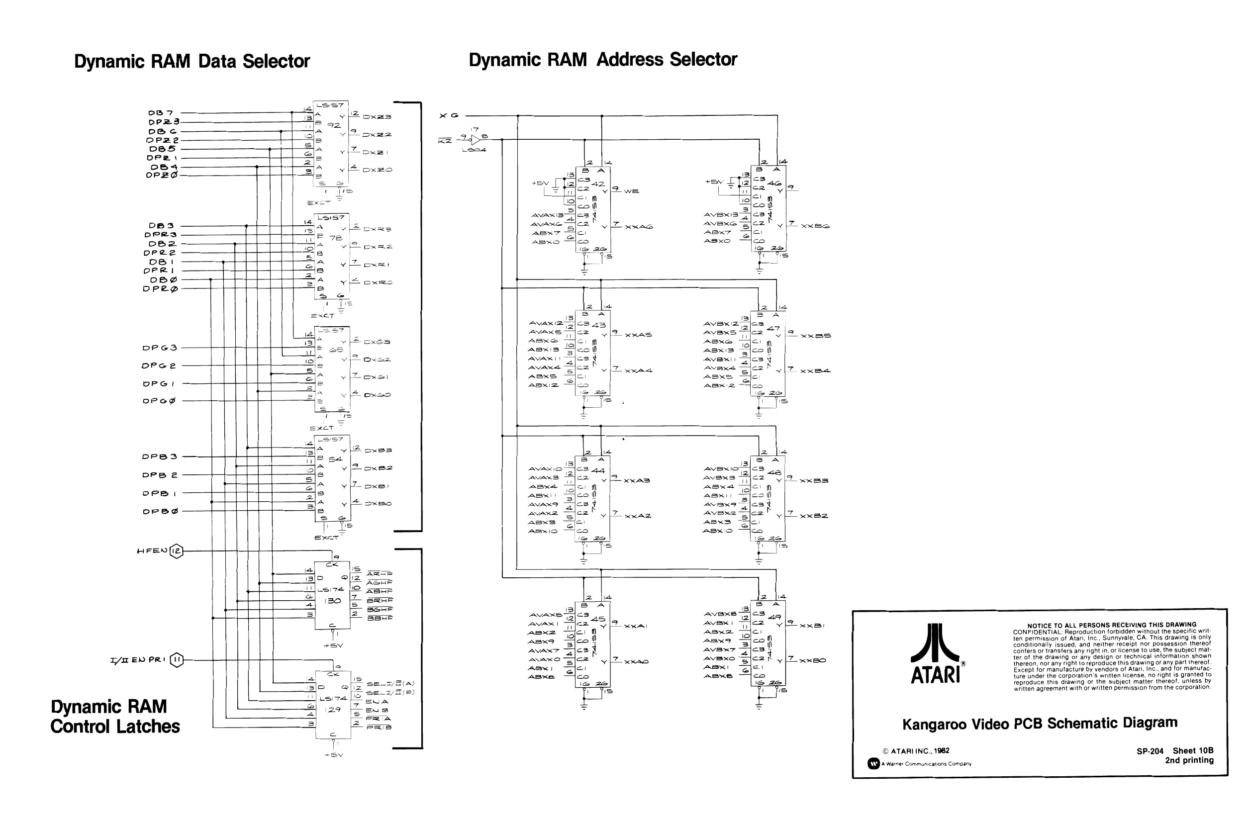
This page is a drawing, shown as the original scan.
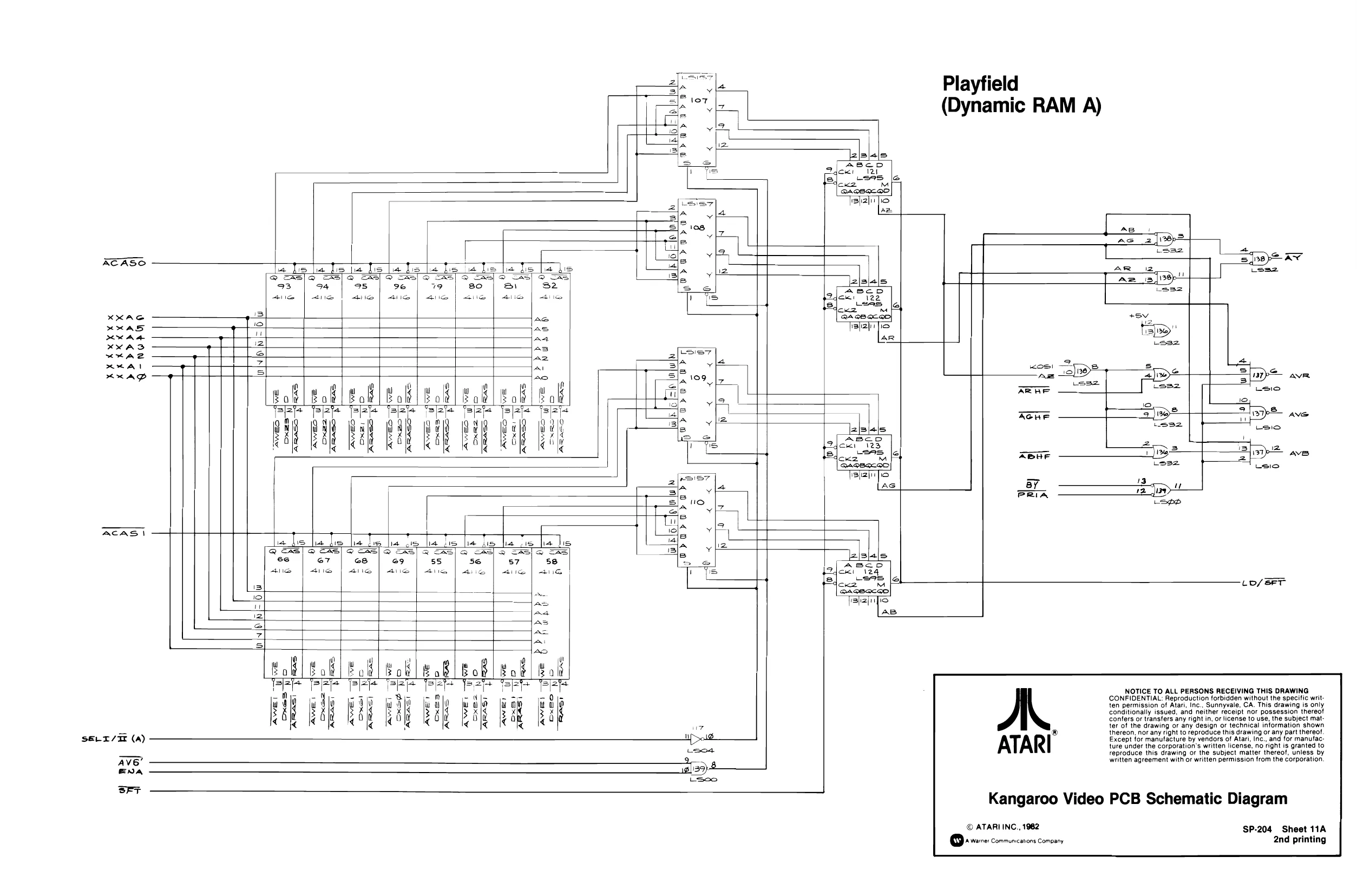
This page is a drawing, shown as the original scan.
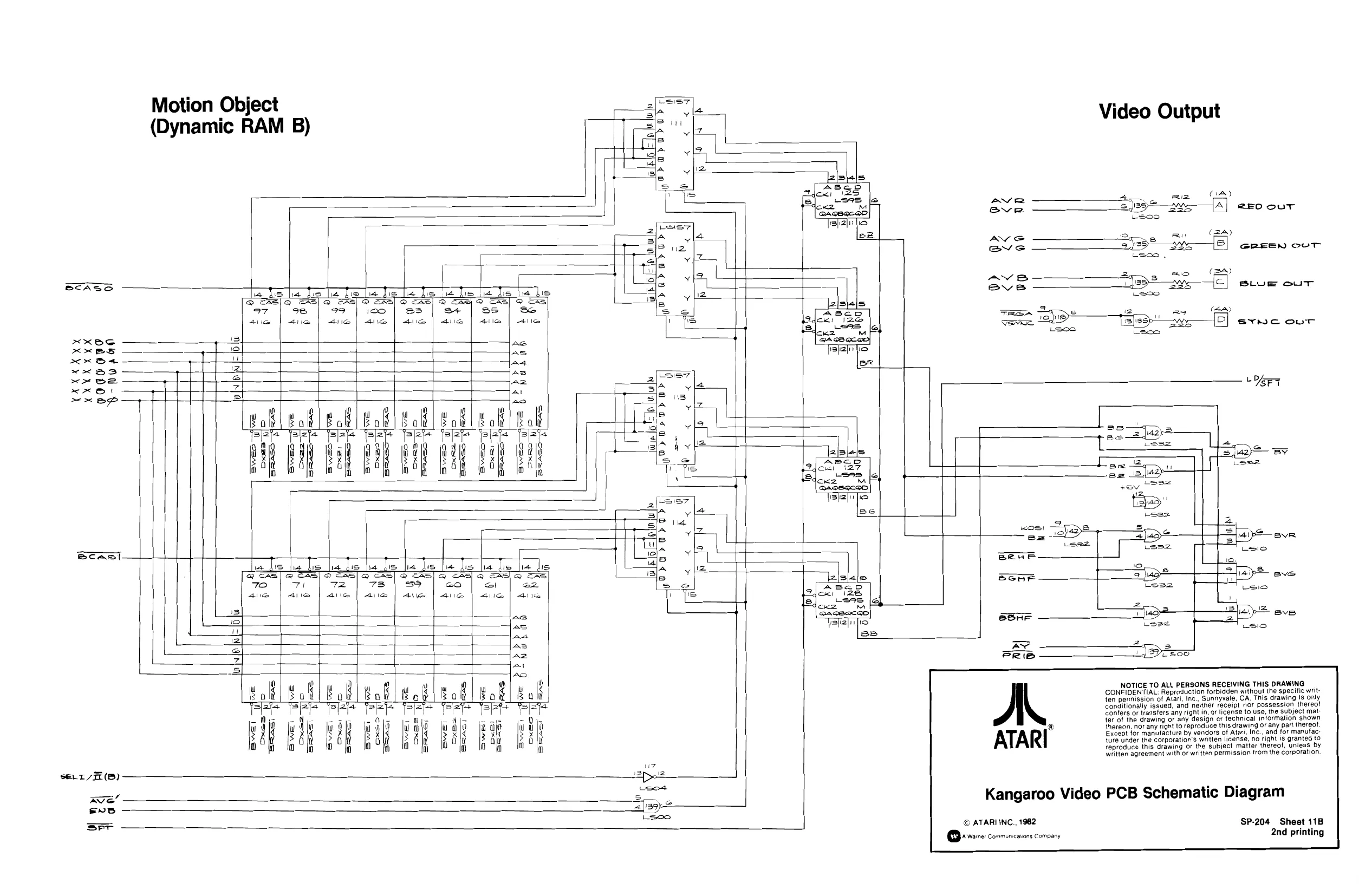
This page is a drawing, shown as the original scan.
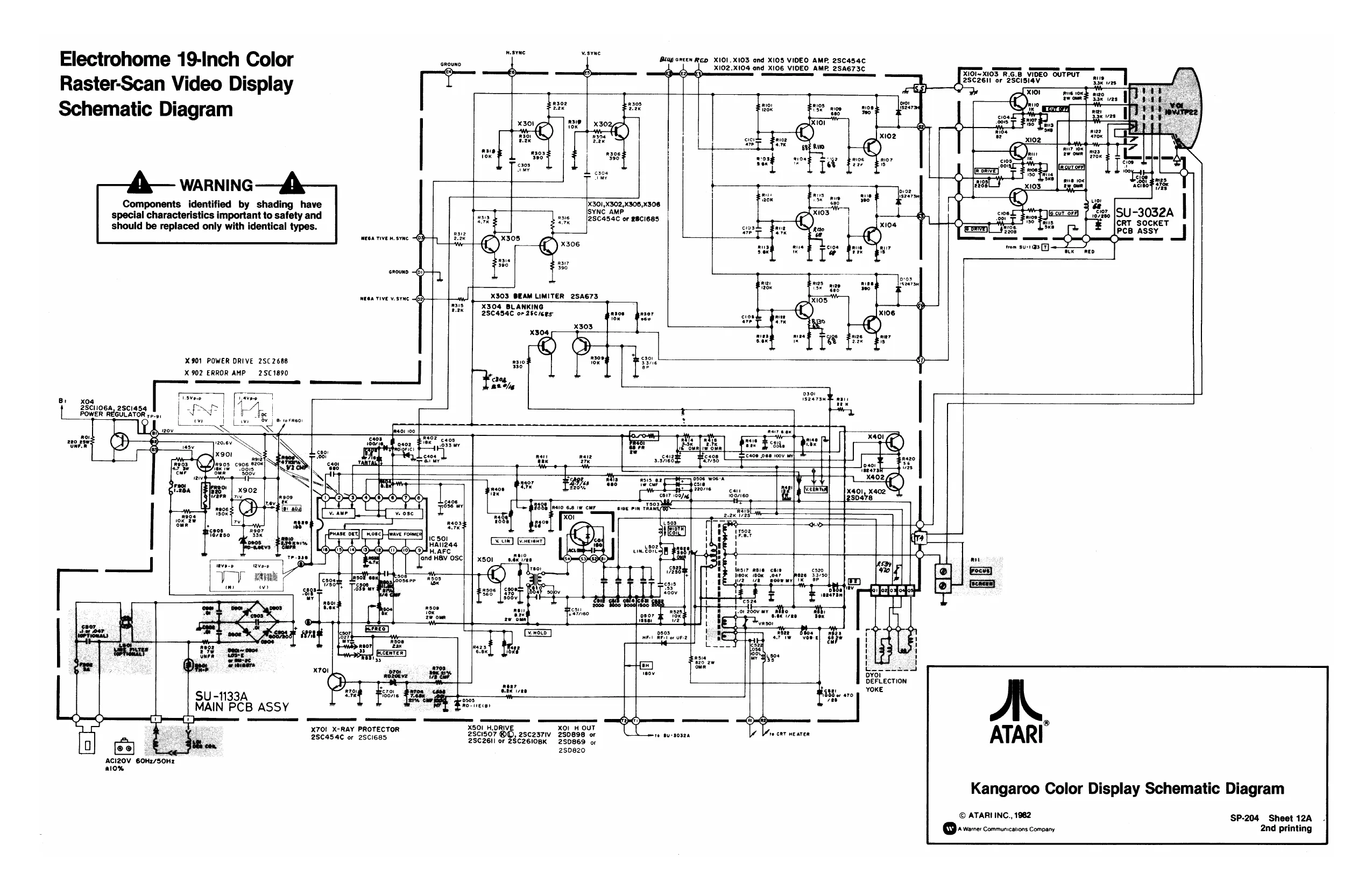
This page is a drawing, shown as the original scan.