Red Baron DP-169-1st-01A
Red Baron (revised hardware) (Atari, 1980) · Drawing Package · 1 pages · original scan
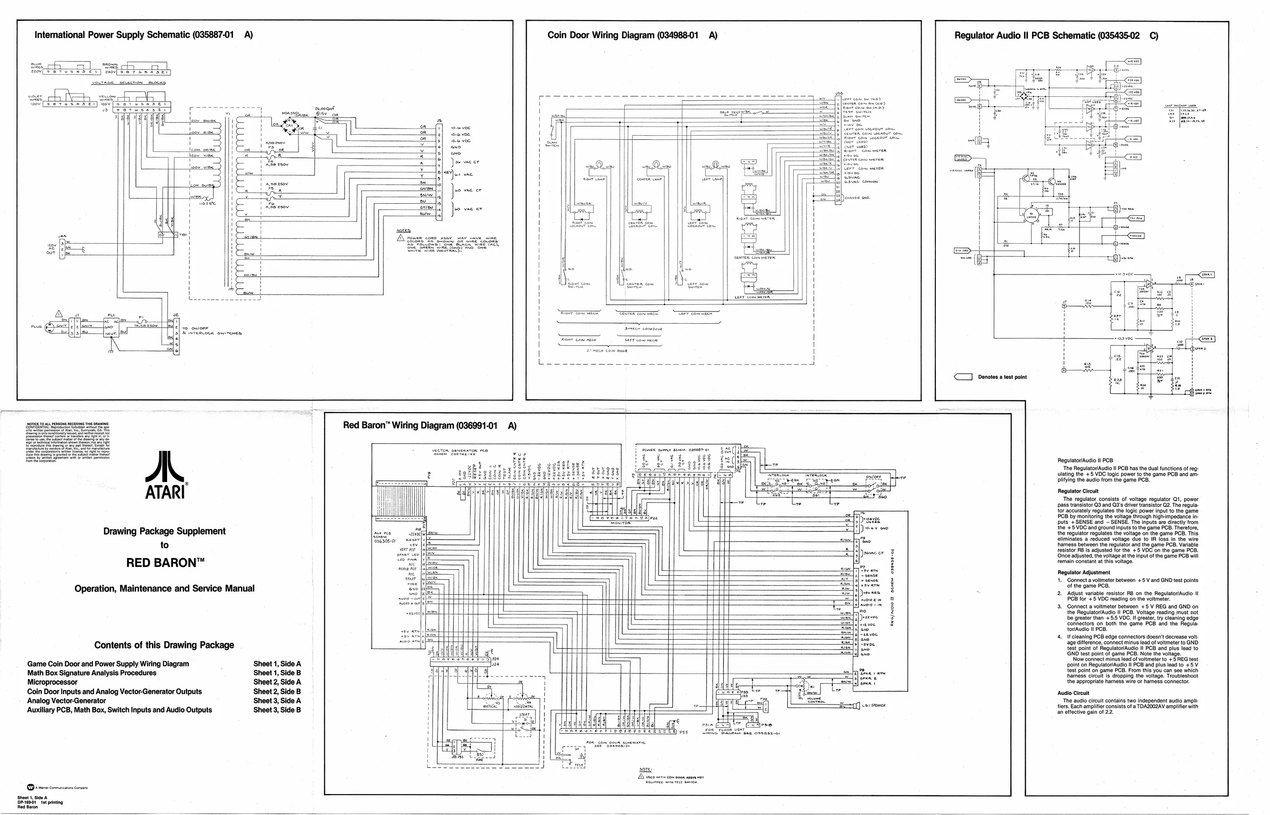
Intemational Power Supply Schematic (035887-01 A) Coin Door Wiring Diagram (034988-01 A) Regulator Audio Il PCB Schematic (035435-02 C)
ray AN cogs, eager, peas tan Ls we PE oor {Se
cl]
<7 denotes « test point
Samoa esa ene erate Red Baron” Wiring Diagram (036991-01 A)
RegulatoriAudio i! PCB ‘The Regulator/Audio ll PCB has the dual functions of reg- Ulating the +5 VDC logic power to the game PCB and amplifying the audio from the game PCB. Regulator Circuit The regulator consists of voltage regulator Q1, power pass transistor Q3 and 03's driver transistor Q2. The regulator accurately regulates the logic power input to the game PCB by monitoring the voltage through high-impedance in puts +SENSE and — SENSE. The inputs are directly from the +5VDC and ground inputs to the game PCB, Therefore, the regulator regulates the voltage on the game PCB. This ‘eliminates a reduced voltage due to IR loss in the wire hhamess between the regulator and the game PCB. Variable ATARI ll Drawing Package Supplement porece coach Satis aneer to sev
| ver | | | y | Testor Ris agjusted forthe +3 VOG on the game PCB. | ||
| ser che | 3 | 3 | ‘nee acjsted, the votage at he input ofthe gare POS wil | ||
| RED BARON™ | eres | Is | H | remain constant a hi voltage. | |
| ve | se] | 3 | Regulator Adjustment | ||
| ae | 3 | 1. Connect aolmeter between +5 Vand GND test pints | |||
| Servi | nm | 3 | of the game | ||
| Operation, Maintenance and | ice; Manual | nae {g|}oveee | & | 2. | Adjust variable resistor RB on the Regulatorfulo It |
| a} | ren | PB for +5 VBC reading on the voltmeter | |||
| Ee | flaoeiin | 3 | 3. | Connect a voitmeter between +6 V REG and GND on | |
| 7 | 0 | 2 | ‘the Regulator/Audio Il PCB. Voltage reading must not | ||
| Tisr|s|)reevoee | > | be greater than +5. VDC. If greater, try cleaning edge | |||
| “wit 4} +12 yoo. | g | connectors on both the game PCB and the Regula: | |||
| Eroa | Bey | fonaudio | PCB | ||
| capt | 4 | If cleaning PCB edge connectors doesn't decrease: | |||
| Contents of this Drawing Package | SE | | | siete oe ra | ie | aN |
=e Now connect misustead of vatnetort6 +S REG test (ow connect minus ts
| Game Coin Door and Power Supply Wiring Diagram | Sheet 1, Side A | point on ReguiatorAudio i PCB and pis lead to +5 | ||
| Math Box Signature Analysis Procedures | Sheet 1, Side B | 4] bond yen | Pe | |
| Microprocessor | Sheet 2 Side A | ai | ret * | the appropriate hamese wire or hamess connector. | |
| Coin Door Inputs and Analog Vector-Generator Outputs | Sheet 2, Side B | ne | ‘Audio Ciruit | |
| Analog Vector-Generator | Sheet 3, Side A | Sa | sf] sie | ‘The audio circuit contains two independent audio ampli- |
| Auxiliary PCB, Math Box, Switch Inputs and Audio Outputs | Sheet 3, Side B | Ser | am sroelier cones of &,TOAEOIZAY erp | wth |
tome consom smavor Daven comes cover ‘Sheet 1, ise A Brot et pintng