Flim-Flam
Flim-Flam (Meadows Games Inc.) · Manual · 37 pages · 58 sections · original scan
This page carries no recoverable text. It is a drawing or a photograph. See the original scan.
FLIM-FLAM MANUAL
MEADOWS GAMES INC. 181 COMMERCIAL e SUNNYVALE, CALIFORNIA 94086 e PHONE (408) 732-8110
INTRODUCTION AND WARRANTY INFORMATION
Flim Flam is a coin operated video amusement device which ac-
curately simulates the experience of a doubles tennis match.
The game may be operated by two, three, or four players simul-
taneously and accommodates groups of players who have differing
degrees of skill.
The electronics of this game incorporates the latest advances in
semiconductor technology resulting in long life and low maintenance.
However - as with all devices mechanical or electrical - there will
inevitably be minor problems. This manual describes all adjustments,
repairs, and troubleshooting procedures which you will need to know
to operate the game,
If the printed circuit board (PCB) fails within the one-year warranty
period, immediately contact for repair
and replacement instructions. NOTE: Any PCB repair attempted by
anyone other than factory authorized service personnel will void
PCB warranties. If your computer PCB fails after the warranty expires,
it will be repaired for a nominal parts and labor charge.
The TV monitor is under warranty for a period of thirty days and if the
monitor should fail within this period, immediately contact
for repair and replacement instructions. NOTE:
Page 1
Any TV monitor repairs attempted by anyone other than factory author-
ized service personnel during warranty period will void TV monitor
warranty. If the TV monitor fails after the warranty period has
expired, we recommend having service performed by any reputable TV
repair shop.
NEW MACHINE SET-UP AND CHECK-OUT PROCEDURES
After uncrating, save all packing materials in the event machine needs
to be returned.
As each new Flim Flam leaves the factory, every component and sub-
assembly is carefully checked for proper operation. However, since
parts may have been damaged or factory adjustments changed due to
shaking and jarring during shipping, the following check-out pro-
cedure must be performed prior to placing the machine on location.
a. With the machine unplugged, open coin acceptor door and raise the
top by removing wing nut hold down. Carefully inspect both the ex-
terior and interior for any obvious damage to the cabinet or internal
components which may have occurred during shipping. If any such
damage is discovered, immediately contact the freight carrier. Then
contact for repair or replace-
ment instructions.
b. Inspect the interior of the machine more carefully, looking for
Page 2
broken or disconnected wires, sub-assemblies not securely mounted,
and any foreign objects shorting or interfering with electrical
connections. Pay particular attention to the connections to the TV
monitor, the players' controls, and the coin switch. Check the se-
curity of the computer PCB and flasher PCB edge connectors.
c. Plug the machine in and check the CRT (Cathode Ray Tube) image
which should be steady, centered, sharp, and exhibit the proper
levels of brightness and contrast. With the machine plugged in, but
not started, the CRT will display the Attract Mode (see next section
for Attract Mode explanation).
d. Insert several old and new coins into the coin acceptor. No
genuine coin should be rejected. Operate the coin return button
while checking for signs of stickiness or binding. Lightly spray
the coin acceptor, return button and the inside of both lock cylinder
with WD-40, a silicone lubricant.
e. Check the computer for proper operation by playing several games
and compare the results with the game sequence analysis in the next
section.
THE GAME SEQUENCE
with the game plugged in but not started, the CRT will display the
Attract Mode. Durring Attract, the general illumination lamps are
Page 3
lighted, the attract lamps flash, and the ball rebounds off the
playfield walls.
Coin insertion produces game credit and the players may select
either the Two Player Mode or the Four Player Mode by depositing
one (25¢) or two (50¢) coins. The game is started by pressing one
of the paddle size buttons.
THE TWO PLAYER MODE
If only one coin is inserted, the Two Player Mode will automatically
be selected by the computer and the two player configuration will
appear on the CRT after one of the paddle size selector buttons is
pressed. These buttons control the relative difficulty of the game
by changing the paddle size.
The two player CRT configuration consists of a playfield bounded by
walls on all four sides, a dotted net line separating the players'
courts, two paddles (one for each side) and the score remaining
from the last game. The attract lamps do not flash during the play
mode. The score is reset to zero at the beginning of each game and
will count to a maximum of 11 or 15, depending on the position of the
score switch. The ball is automatically served from the middle of
the CRT and is manipulated by placing the paddle directly in the path
of the ball. The direction the ball is bounced is controlled only by
where the ball strikes the paddle. For instance, if the ball encounters
Page 4
the uppermost portion or "segment" of the paddle, it will be bounced
upward at the maximum angle. "Striking" the ball with a moving paddle
will not produce a greater or different effect than simply placing the
paddle in the path of the ball. There are two ball speeds: the normal
or "slow" speed, and the "fast" speed produced by pressing the speed
buttons. The speed button will produce this effect only after the
ball has been hit, and pressing this button causes the ball to
drastically shift horizontally.
THE FOUR PLAYER MODE
Two coins (50¢) must be deposited to produce the four player config-
uration which will appear on the CRT when the desired size button is
pressed. In this configuration, an additional horizontal net line
divides the playfield into two sections. Four paddles appear and
each paddle is permitted movement only within its own quadrant.
Other than these differences in the CRT display, the four player
game sequence is identical to the two player sequence.
SCORE ADJUSTMENT
A maximum score of 11 or 15, may be operator selected by changing
the position of the slide switch found in the bottom right hand
corner of the computer PBC (Figure 1). If the switch is in the
right hand position, the game will end at 11 points. Sliding the
switch to the left endsgame at 15, which is the recommended setting.
Page 5
‘TV MONITOR ADJUSTMENT
The TV monitor adjustments function like those of the home TV Set.
Refer to monitor manual for the locations of the following adjust-
ments.
a. VOLUME: Adjust the volume to the preference of the location.
Beep in mind that the machine will sound louder with the control panel
raised.
b. BRIGHTNESS: Brightness is adjusted before contrast. Adjust so
the CRT background is as dark as possible without diminishing the
brightness of the playfield walls.
c. CONTRAST: Adjust so that the CRT images are as bright as possible
against the pre-adjusted dark background without blurring.
a. VERTICAL HOLD: Adjust only if the picture appears to be rolling
up or down the screen. Adjust for a stable, centered picture.
e. HORIZONTAL HOLD: Adjust if the picture appears to be shifted off
center horizontally, the images are warped, or if the whole picture
is broken into diagnol lines.
PADDLE ADJUSTMENT
For reference the lower side of court is nearest coin operator. The
upper side of court is nearest the game's scores. The left and right
sides of court are as you face the coin operator.
Paddle should be checked every service call. Paddle will need adjust-
ing when a pot or logic board has been replaced. If a pot has been
replaced refer to section on preliminary adjustment. Each paddle has
three adjustments:
Page 6
- Right Horizontal Position
- Upper Vertical Position
- Lower Vertical Position
When adjusting, set four play mode using "pro" size paddles.
To adjust horizontal position, move joystick to extreme right position.
Rotate horizontal pot on joystick assembly (Figure 2) until the paddle
is just inside its right hand boundary.
To adjust top vertical position, move joystick to its extreme upper
position. Turn pot on joystick (Figure 2) until the paddle is at
its upper boundary.
To adjust lower vertical, move joystick to its extreme lower position.
Turn pot on logic board (Figure 1) so that the paddle is at its
lower boundary. This adjustment may disturb upper vertical position.
Further adjustment may be necessary. Repeat procedure for each of the
four paddles.
PRELIMINARY ADJUSTMENT
The joystick pots need preliminary adjustment if the pots have been
replaced. Preliminary adjustments should be done before the joystick
is remounted.
a. ADJUSTING 2 PLAYER JOYSTICKS: Rotate pots of joystick Counter-
Clockwise until the stick is forced to move and the pot will not rotate
Page 7
any further. Now apply slight pressure to the stick and move it ina
circular motion. The joystick is ready for mounting in the unit. Wires
must be connected to termimals #1 and #2 on the pots.
b. ADJUSTING 4 PLAYER JOYSTICKS: Rotate pots of the joystick Clockwise
until the stick is forced to move and the pot will not rotate any
further. Now apply slight pressure to the stick and move it ina
circular motion. The joystick is ready for mounting in the unit. Wire
must be connected to terminals #2 and #3 on the pots.
COIN ACCEPTOR OPERATION, ADJUSTMENT AND MAINTENANCE
The detection and rejection of undesired or counterfeit coins are
determined by size (both thickness and diameter), weight, and
metallic composition.
The transfer cradle (#9 in Figure 4) is used to test both the size and
weight of the coin. The quarter must first pivot an "undersize" lever
- to unlock the transfer cradle and can be returned by actuating
the wiper operating lever (17). Oversize diameter coins will fail to
Pass between the transfer cradle and the wiper and can be returned by
operating the wiper lever. Coins that are oversize in thickness will
fail to pass between the magnet gate (11) and the main channel (5) and
will have to be dislodged by actuating the wiper operating lever.
Underweight coins will fail to overcome the transfer cradle counter-
weight and can be returned by operating the wiper lever.
Page 8
A magnet is used to test the metallic composition of the coin.
Highly magnetic coins, such as steel or iron, will be retained by
the magnet and can be returned by actuating the wiper operating lever.
Coins having comparatively high magnetic properties will be slowed
down by the magnet and will drop off the rail short of the Accept
entrance and will be returned. Coins having little or no magnetic
properties, such as brass or zinc, will pass through the magnetic field
so fast they will overshoot the accept entrance and will be returned.
ADJUSTMENT
All coin acceptors leave the factory adjusted for maximum performance.
If, however, more critical adjustment is desired, or if the unit has
been disassembled for cleaning, the following adjustment procedure is
suggested.
KICKER AND SEPARATOR
a. Set the acceptor on a level surface with the back of the unit facing
you (the kicker and separator are on the back).
b. Loosen the screws holding the kicker (1) and the separator (3) and
move both the kicker (2) and the separator (4) as far to the right as
they will go. Tighten the screws lightly.
c. Insert several test coins (both old and new) and note that some are
returned by striking the separator.
d. Loosen the separator screw and move the separator a slight amount to
the left. Retighten the screw.
Page 9
e. Insert the test coins again, and if some are still returned, repeat
Step D until all the coins are accepted.
f£. Loosen the kicker screw and move the kicker a slight amount to the
right. Retighten the screw.
g. Insert the test coins again and, if some of them are returned, re-
peat Step F until all coins are accepted.
h. Be sure that both screws are tight after the adjustments have been
made.
THE MAGNETIC GATE
a. Set the acceptor with the front of the unit facing you in the test
position.
b. Turn the magnet gate adjustor (12) out (counter-clockwise) until
none of the coins will fit through.
¢. With a coin resting in the transfer cradle, turn the adjustor in
(clockwise) until the coin barely passes through the magnet gate.
d. Test this adjustment using several coins, and if any fail to pass
through the magnet gate, repeat Step C until all coins are accepted.
e. Fix the magnet gate adjustor in this position with a drop of glue
or Loctite, if necessary.
ACCEPTOR MAINTENANCE
Depending on the enviornment in which the acceptor is used, periodic
preventative maintenance should be performed.
Page 10
The mainplate (5) may be cleaned with any household cleaner. Thorough
rinsing and drying are necessary to remove deposits and/or film. Re-
move all metal particles from the magnet by guiding a screwdriver along
the edges of the magnet. Remove the transfer cradle and undersize lever
and clean the bushings and pivot pins and bushings and re~assemble.
Spray the entire unit lightly with wWD-40, a silicone lubricant.
TROUBLE SHOOTING HINTS
TESTING COMPONENTS OF GAME
Buttons & Coin Switch are normally open. When pushed they are closed.
The buttons can be by-passed by touching the wires together.
Harness can be tested by an ohm-meter or continuity checker.
Fuses are checked by a visual inspection or continuity checker.
Flasher Board assembly can be checked by first measuring proper voltages
on wires from flasher board. See figure diagram, Dwg 25-0001.
Logic Board & T.V. Monitor can be checked by substitution of a good
replacement. Repair of Logic Board & Monitor should only be serviced ‘by
experienced technicians.
NO PICTURE: Check .if back of picture tube is lit. If not, inspect
fuses, power cord, and power outlet. If these are good and tube is not
lit repair of monitor is necessary.
Pagell
If the tube is lit , check adjustments of brightness and contrast.
Test continuity of logic board pins #1 and #3 (5th volt dc power supply},
and pin #5 (Video output). If all check out, problem is either the
logic board or monitor.
NO SOUND: Check adjustment of volume control on T.V. monitor. Test
continuity of logic board pin #17 (audio signal), and monitor pins #5
and #8. Check speaker, logic board, and T.V. monitor.
NO BALL: Coin acceptor switch may be shorted or jammed. Wires from
logic board pin #16 and #22 may be shorted. Replace logic board.
NO PADDLES: Check paddle adjustment. Test continuity of wires, from
pots to logic board. The game may not be resetting properly. Check
coin switeh and wires. Check pots and logic board.
PADDLE DEFECTS: If paddles appear and are jumpy, oscillating, flick-
ering, or will not stay within its boundaries, pots may need adjustment
or replacement.
SCORE: If game shuts off at scores other than 11 or 15, the selection
switch may be dirty. Use a contact or switch cleaner on switch.
GAME DEFECTS: If game is not operating properly, for example: incorrect
scoring segments missing, erratic ball movement, the likely cause is the
logic board.
FLIM FLAM SPEED BALL : Check speed buttons & wires. Check logic board.
Pagel2
pur escription Tare [APPROVED _|
Left Two Player JOYSTICK ADJUSTMENTS (FIGURE # 2)
Right Two Player Paddle
Speed Button
Right Four Player
Pe
addle Vertical Pot
Left Four Player
Horizontal Pot
Score Switch TOLERANCES UNLESS OTHERWISE SPECIFIED FRACTIONS DEC ANGLES} LOGIC BOARD AND JOYSTICK
+ + + ee ae al || 00 NOT SCALE DRAWING MEADOWS GAMES, INC.
JOYSTICK ASSEMBLY
EXPLODED VIEW
FIGURE 3 TOLERANCES UNLESS
OTHERWISE SPECIFIED
FRACTIONS DEC ANGLES MEADOWS CAMES, INC.
bw x: |
JOYSTICK ASSEMBLY,
EXPLODED viEw
REVISIONS
KICKER SCREW DESCRIPTION DATE | __APPROVED _|
KICKER
SEPARATOR SCREW
SEPARATOR
MAINPLATE ASSEMBLY
GATE ASSEMBLY
COVERPLATE ASSEMBLY RAIL CRADLE ASSEMBLY UNDERSIZE LEVER MAGNET GATE ASSEMBLY MAGNET GATE ADjUSTER SCREW LOWER GATE PIVOT SPRING UPPER GATE PIVOT SPRING GATE PIVOT PIN WIPER LEVER SPRING WIPER LEVER WIPER ramen on ane 1S WwW FIGURE 4 COIN ACCEPTOR — EXPLODED
[TOLERANCES UNLESS: OTHERWISE SPECIFIED FRACTIONS DEC ANGLES| Coin Acceptor Exploded View DRAWING NO. FIGURES — COIN FACE PLATE [G-O004
REVISIONS
pum[ oO escriprion CATE APPROVED |
Pin #12 on T.V. 10.8 Volt DC SCALE SIZE [DRAWING NO. = aed 25-0004
REVISIONS
2PLAYER 4 PLAVE
is nt a SS ce : HX SREB Se [ LTR | DESCRIPTION [DATE | APPROVED
LEFT SPEED
Pc, BOARD
EDGE CONNECTOR
TOLERANCES UNLESS
OTHERWISE SPECIFIED MEADOWS GAMES
FRACTIONS DEC ANGLES BUNNYVALE, CA.
- = WIRING HARNESS DINE BARA Pe eY | 1 [121%] FLIM-FLAM COCKTAIL TABLE DO NOT SCALE DRAWING
MANUAL 68P65130A70-1 CHASSIS 19VP111 + “MODEL XM501-10
FILE VP12 XM701-10
23VP111
PART NO, 68765130A70-1 MOTOROLA
service manual
GENERAL INFORMATION
These models are transistorized monitors designed for the video game market. They are identical except for the CRT size. See V1 in Replacement Parts List.
Circuitry includes four stages of video amplification, a two stage audio amplifier, sync and deflection circuits and a regulated power supply. An additional 5 volt 3 amp supply is included to power external logic systems, The picture tube is a 114 degree deflection CRT with implosion protection, Composite video is fed to the monitor through a connector mounted on the rear of the chassis.
Rear panel controls include Horizontal Hold, Vertical Hold, Contrast, Brightness, Volume and width controls, Additional service controls are mounted on the piated circuit panel, and are accessible from the rear of the chassis.
3-75 FILE VP12
The chassis utilizes plug-in etched panel construction with components mounted on the top side and piated wiring on the bottom. Component reference numbers and circuit legend are printed on the board to aid in servicing. Horizontal, vertical output and regulator transistors are mounted on the chassis base which also serves as a heat sink and CRT support.
ELECTRICAL SPECIFICATIONS
Power Rating: 110 watts nominal. 50 watts without 5 volt supply.
Source: 120/240V AC at 50/60Hz Switch selected.
Video Input: PP (sync negative).
Audio Output: 5 watts peak
Display Products
PRICE 80 CENTS 0.5 to 2.5 volts composite
COPYRIGHT 1974 BY MOTOROLA INC. DISPLAY PRODUCTS
CHASSIS
19VP111 23VP111
MODELS
XM501-10 XM701-10
NO WORK SHOULD BE ATTEMPTED ON ANY EXPOSED MONITOR: CHASSIS BY ANYONE NOT FAMILIAR WITH SERVICING PROCEDURES AND PRECAUTIONS.
TABLE OF CONTENTS
CHASSIS PARTS LOCATION .......... 8-11 CHASSIS SCHEMATIC DIAGRAM .......-....- 12 REPLACEMENT PARTS LIST 2.2... -...--.-- 13,14 SAFETY WARNING ....... 2 SERVICENOTES ......... 7 THEORY OF OPERATION
MOTOROLA INC. CAROL STREAM, ILLINOIS 60187
PRINTED IN U.S.A.
SAFETY WARNING
- SAFETY PROCEDURES should be developed by habit so that when the technician is rushed with repair work, he automatically takes precautions.
- A GOOD PRACTICE, when working on any unit, is to first ground the chassis and to use only one hand when testing circuitry. This will avoid the possibility of carelessly putting one hand on chassis or ground and the other on an electrical connection which could cause a severe electrical shock
- Extreme care should be used in HANDLING THE PICTURE TUBE as rough handling may cause it to implode due to atmospheric pressure (14.7 Ibs. per sq. in). Do not nick or scratch glass or subject it to any undue pressure in removal or installation. When handling, safety goggles and heavy gloves should be worn for protection. Discharge picture tube by shorting the anode connection to chassis ground (not cabinet or other mounting parts) When discharging, go from ground to anode or use a weil insulated piece of wire. When servicing or repairing the monitor, if the cathode ray tube is replaced by a type of tube other than that specified under the Motorola Part Number as original equipment in. this Service Manual, then avoid proionged exposure at close range to unshielded areas of the cathode ray tube. Possible danger of personal injury from unnecessary exposure to X-ray radiation may result.
4.-An ISOLATION TRANSFORMER - should always be used during the servicing of a unit whose chassis is connected to one side of the power line. Use a transformer of adequate power rating as this protects the serviceman from accidents resulting in personal injury from electrical shocks. It will also protect the chassis and its components from being damaged by accidental shorts of the circuitry that may be inadvertently introduced during the service operation
- Always REPLACE PROTECTIVE DEVICES, such as fishpaper, isolation resistors and capacitors and shields after working on the unit
- If the HIGH VOLTAGE is adjustable, it should always be ADJUSTED to the level recommended by the manufacturer. If the voltage is increased above the normal setting, exposure to unnecessary X-ray radiation could result. High voltage can accurately be measured with a high voltage meter connected from the anode lead to chassis.
- BEFORE RETURNING A SERVICED UNIT, the service technician must thoroughly test the unit to be certain that it is completely safe to operate without danger of electrical shock. DO NOT USE A LINE ISOLATION TRANSFORMER WHEN MAKING THIS TEST.
In addition to practicing the basic and fundamental electrical safety rules, the following test, which is related to the minimum safety requirements of the Underwriters Laboratories should be performed by the service technician before any unit which has been serviced is returned.
a 1000 OWMIVOLT (OR HIGHER) AC VOLTMETER
NOTES. 1 REPEAT EACH CHECK WITH THE LINE CORD REVERSED
IN THE POWER OUNLET,
- METER READING MUST NOT EXCEED 7-1/2 VOLTS AC. “MOT” LEAD OF METER TO EACH ©KPOSED PART OF CABINET. AS WELL AS THE CABINET. ‘GROUND LEAD OF METER TO ANY EARTH | GROUND SUCH AS A COLD WATER PIPE a. VOUTSAC Gao
INSULATOR we
Voltmeter Hook-up for Safety Check
A 1000 ohm per volt AC voltmeter is prepared by shunting it with a 1500 ohm, 10 watt resistor. The safety test is made by contacting one meter probe to any portion of the unit exposed to the operator such as the cabinet trim, hardware, controls, knobs, etc., while the other probe is held in contact with a good “‘earth’’ ground such as a cold water pipe.
The AC voitage indicated by the meter may not exceed 7% volts. A reading exceeding 7% volts indicates that a potentially dangerous leakage path exists between the exposed portion of the unit and “earth” ground. Such a unit represents a potentially serious shock hazard to the operator.
The above test should be repeated with the power plug reversed, when applicable.
NEVER RETURN A MONITOR which does not pass the safety test until the fault has been located and corrected.
TH EORY OF OPERATION CRT DISPLAY MODULE - COMPOSITE VIDEO SYSTEM VP12
COMPOSITE BRIGHTNESS
VIDEO VIDEO AMP INPUT —>
VERTICAL HIGH O56 VOLTAGE a SUPPLY VERTICAL ourPuT SYNC SEPARATOR
HORIZONTAL OSCILLATOR HORIZONTAL HORIZONTAL aorpur
15,500 - 16,000H2
Block Diagram
POWER SUPPLY
The power supply is a transformer operated, full wave, regulated supply which maintains constant output voltage with input variations of +15%. A switch (SW1) is provided to allow operation from 115/230 volts, 50/60Hz. The regulator is a series pass circuit. Q16 is the series pass transistor, Q15 the reference amplifier and Q74 the output driver.
” The output voltage of the regulator appears at the emitter of Q16. This voltage is divided between R71, R74 and R73. The voltage appearing on the arm of potentiometer R74 is a reference input to the base of Q15.
A temperature conpensated zener diode (D6) is used to establish a fixed reference voltage at the emitter of Q15. R72 provides a bias current for D6, establishing its operating point.
An increase in output voltage will result in an increase of voltage at the base of Q15. Since the emitter of Q15 is held ata fixed reference voltage, the change in base voltage will turn Q15 on harder, reducing its collector voltage. This reduces forward bias for Q14 resulting in less emitter current and less base current for Q16, Q16 will conduct less, lowering the output voltage.
R79 provides a shunt current path for Q16 allowing it to run cooler, improving reliability. C44 is an RF noise filter.
A fixed, regulated 5V DC supply is used to power circuits external from the monitor. Its operation is similar to the 73V regulator except for the reference amplifier which is contained in the IC package.
a a 3
157 VIDEO AMP 2ND VIDEO AMP. VIDEO outeUT
fee coy, KIL 120
1 cae teat ax
VIDEO AMPLIFIER
The video amplifier has four stages incorporating devices Q1, Q2, Q3 and Q4, The first stage, Q1, functions as an emitter follower. The low output impedance of the first stage permits use of a low resistance contrast control which furnishes flat video response over its entire range without the need for compensation. The collector output of Q1 is used to drive the sync separator. C3 provides high frequency roll off to limit the collector output to the bandwidth required to pass synchronization signals. Q2 is a common emitter stage and is directly coupled to Q4. Q3 and Q4 are connected in a cascode configuration. This common emitter-common base connection greatly reduces the effect of Miller capacity compared with a conventional single transistor video output stage. C6 provides a ground for video at the base of Q3, the grounded base transistor of the video output cascode pair. Diodes D13 and D8 provide temperature compensation for the video output stages, and diode D23 protects Q1 from transients.
The video bias control R10, is used to set the quiescent collector voltage of Q3. C5, C7, C8 and R15 are used for high frequency compensation. The video amplifier output is direct coupled to the control grid of the CRT through R18 which is used to isolate Q3 from transients that may occur as a result of CRT arcing.
SYNC SEP R98 220
| SYNC SEPARATOR | FROM. | Clly/. |
| The sync separator employs a single stage, Q5, to recover sync | a | 0068 |
from the composite video signal. A single stage sync separator is adequate due to the high impedance of the following stages. The video input to the sync separator is black positive. C11 is charged by the peak base current that flows when the positive peak of the input takes Q5 to saturation. This charge depends ‘on the peak to peak input to Q5 and thus makes the bias for Q5 track the amplitude of the input signal. As a result Q5 amplifies only the positive peaks of the input signal. The initial bias current through R24 sets the clipping level. R98 is used for transient protection. REFERENCE
| PHASE DETECTOR | ‘ | eyne |
The Phase Detector consists of two diodes in a keyed clamp OSC ON FREQ
| circuit: Two inputs are required to generate the required | BO | NO CORRECTION |
output, one from the sync separator and one from the horizontal deflection system. The required output must be of VOLTAGE DEVELOPED
| the correct polarity and amplitude to correct phase differences | c | OSC SLOW,POS |
| between the input sync and the horizontal time base. The | 0 | CORRECTION VOLTAGE |
horizontal collector pulse is integrated into a sawtooth by R45
| and C15. During sync time both diodes in D7 conduct, | a | OSC FAST,NEG |
shorting C15 to ground. t) ~~ CORRECTION VOLTAGE
The sawtooth on C15 is thus clamped to ground at sync time. If the horizontal time base is in phase with the sync, the sync pulse will occur when the sawtooth is passing through its AC axis and the net charge on C15 will be zero. (Figure B). If the horizontal time base is lagging the sync, the sawtooth on C15 will be clamped to ground at a point negative from the AC axis. This will result in a positive DC charge on C15. (Figure C). This is the correct polarity to cause the horizontal oscillator to speed up to correct the phase lag.
Likewise, if the horizontal time base is leading the sync, the sawtooth on C15 will be clamped at a point positive from its AC axis, resulting in a net negative charge on C15 which is the required polarity to slow the horizontal oscillator (Figure D). R30, C17, C16 and R32 comprise the phase detector filter. The bandpass of this filter is chosen to provide correction of horizontal oscillator phase without ringing or hunting. Capacitor C23 times the phase detector for correct centering of the picture on the raster.
VP12
HORIZONTAL OSCILLATOR HOROSE yak Q6 is employed in a modified type of Hartley oscillator. The operating frequency of this oscillator is sensitive to its base input voltage. This permits control by the output of the phase detector and also by the setting of the horizontal! hold control, R34, The horizontal hold range is set by adjustment of the core of L1. oly R32 33K 2y.05 245, 1506
HoRIZ ouTPur COLLECTOR, PULSE
PULSE SHAPER & HORIZONTAL DRIVER a HR PULSE Q7 is used as a buffer stage between the horizontal oscillator non and horizontal! driver. It provides isolation for the horizontal oscillator as well as a low impedance drive for the horizontal driver. R38 and C20 form a time constant which shapes the 7 oscillator output to the required duty cycle (approximately ay 50%), to drive the horizontal output circuitry. The horizontal driver stage, Q8 operates as a switch to drive the horizontal output transistor through T1. Because of the low impedance drive and fast switching times furnished by Q7, very little power is dissipated in Q8. C21 and R42 provide damping to suppress ringing of the primary of T2 when Q8 goes into cutoff.
HORIZONTAL OUTPUT
The secondary of T1 provides the required low drive o impedance for Q9. R44 and C24 form a time constant i ha
for fast turn-off of the base of O9. Q9 operates as a =a)
switch which, once each horizontal period, connects the jag,
supply voltage across the parallel combination of the n ~s horizontal deflectian yoke and the primary of T2. The required sawtooth of deflection current through the horizontal yoke is formed by the L-R time constant of the yoke and output transformer primary. The horizontal retrace pulse charges C27 through D2 to provide operating voltage for G2 of the CRT. Momentary transients at the collector of Q9, should they occur, are limited to the voltage on C27 since D2 will conduct if the collector voltage exceeds this value, The damper diode, D1, conducts during the period between retrace and turn on of Q9. C28 is the retrace tuning capacitor. C29 blocks DC fram the deflection yoke. L3 is a magnetically biased linearity coil which shapes deflection current for optimum trace linearity. L4 is a series width control. C31 and R49, C42 and R68 are damping network components for the linearity and width controls. C43D is charged through D5 developing the video supply voltage. VERT RIE a? BANKING
| R50 3.3K RBZ IK | R55 22K | R56 39K | os | BLANK |
oe
| Oo | af | 7 | cas |
“ : . T AS
| vent | Osc. | Ys | : | 6 |
; : SS Yore
| (3ty 087 | | | f | on |
R26 =
| Sok TR | car | i | ||
| js | au | a | = | |
| SYNC | = | ER VERT OSC 2 | 22MF | VERTLIN = +30 |
iyPur t R59GK ROD 2.2K ac 7a ne ane RODS Oa
L VERT sg. => = Size 2 VERTICAL OSCILLATOR DRIVER AND OUTPUT -
Sync from the collector of QS is integrated by R26 and C35. Q10 and Q11 are connected as a regenerative switch. The series combination of C37 and C38 charges through R58, R56 and D3 until Q10 turns on. This occurs when the emitter of Q10 exceeds its base voltage and causes current to flow into the base of Q11, turning that device on. When Q10 and Q11 conduct,
C37 and C38 are discharged to nearly zero. Q10 and Q11 then shut off and the cycle repeats. The setting of R82 determines the repetition rate of the charge and discharge of C37 and C38. The waveform generated is a positive going ramp or sawtooth with a fast retrace to zero. D3 provides a smail incremental voltage above ground to overcome the forward sawtooth to a low impedance drive for Q13.
T3 matches the collector of Q13 to the vertical yoke. When Q13 is cut off during vertical retrace, a high voltage pulse is developed across the primary of T3. To limit this pulse to a safe value a varistor, R81, is connected across the primary. R66 and C41 provide damping to shape the collector pulse so it may be used for retrace blanking. Since the primary impedance of T3 decreases with current, the degree to which the primary shunts the reflected load impedance varies with collector current. This would result in severe vertical non-linearity unless some compensation is employed.
Resistors R59 and R60 couple the emitter voltage of
Q13 to the junction of C37 and C38. Since this path
is resistive, the waveform coupled back will be integrated into a parabola by C38. This results in a pre-distortion of the drive sawtooth as shown in Figure C. This is done to compensate for the non linear charging of C37 and C38 and the changing impedance of the primary of T3. An additional feedback path through R62 and C40 serves to optimize the drive waveshape for best linearity.
RETRACE BLANKING Both vertical and horizontal retrace blanking are provided by positive pulses applied to the CRT cathode. The collector pulse from the horizontal output transistor is placed across R23 through R46. The vertical collector voltage is differentiated by C30 to remove the sawtooth portion of the waveform. The remaining pulse appears across R23, The mixed vertical and horizontal pulses on R23 are coupled to the CRT cathode by C10.
AUDIO AMPLIFIER Q17 and Q18 form a DC coupled “switching tone burst amplifier’’. An input signal biases Q17 on, in turn driving Q18 into conduction. When the signal is removed both stages return to a quiescent mode. Coupling capacitor C50, diode D19 and resistor R88 establish a bias voltage which is signal dependent. Volume contro! R85 sets the peak to peak level for the output stage. Lamp ET serves to protect the speaker if the audio output transistor fails, it also protects the transistor should the speaker leads be shorted. Diode D22(on early models)polarizes the speaker insuring proper installation. If it is installed wrong, little or no audio will be developed,
SPOT KILLER Normally Q21 is not conducting and capacitor C51 is charged to the supply voitage. When the monitor is turned off, C51 discharges through R96 turning the transistor on. It in turn removes the positive potential from the brightness control connecting the CRT cathode to ground, causing the tube to conduct hard, discharging the high voltage.
PANEL REMOVAL/INSTALLATION N_A_ PARABOLA H : | AT JUNCTION C37, C38
VERTICAL'DRIVE B! WITHOUT 4 ' VERT PARABOLA ADDED | PARABOLA PULSE AND VERTICAL SAWTOOTH ADDED ., TOGETHER, HENCE PRODUCING THE REQUIRED VERT DRIVING SIGNAL
+15 fA Ral fH R22 270K 17 [| 20K? & cr BLANKING
RE? 18K} VERT IN
| Pl-4, | $2-2__ | VOLUME | 10.8 |
+e a7 —___;
| AUDIO’ = | Ad | se9 | RISO | |
| INPUT | ¢59 | Losey | _yySdrd | : |
| SOF | aus | PIB yn | Yl |
Pa >t
| 529 | AUDIO | 16.0. SPKR | q |
OUTPUT =
Qa R95 10K a SPOT +150V R97 KILLER BRIGHTNESS, To
| CRT | Ral | C51 |
CATHODE 200K] FLOK-FF gome
To prevent damage to the board or foil when removing the circuit panel it may be necessary to pry up slowly, IN STAGES around the edges as shown. Start at one corner and move all around the board keeping the screw driver tip against the chassis. When installing, apply pressure at the edges near the pins. Do not force dawn on the components.
CIRCUIT TRACING Component reference numbers are printed on top and bottom of the plug-in circuit board to facilitate circuit tracing. In addition, control names and board terminal numbers are also shown and are referenced on the chassis schematic diagram in this manual. Transistor elements are identified as follows: E — emitter, B — base, and C — collector. COMPONENT REMOVAL Removing components from the etched board is facilitated by the fact that the circuitry (plating) appears on one side of the board only and the component leads are inserted straight through the holes and are not bent or crimped. It is recommended that a solder extracting gun be used to aid in component removal, An iron with a temperature controlled heating element would be desirable since it would reduce the possibility of damaging the board due to over-heating. The nozzle of the soldering gun is inserted directly over the component lead and when sufficiently heated, the solder is drawn away leaving the lead free from the copper plating. This method is particularly suitable in removing multi-terminal components.
REGULATOR ADJUSTMENT
- Apply test signal to proper input. Signal should be of same amplitude and sync rate as when monitor is in service.
- Adjust vertical and horizontal oscillator controls until display is synced,
- Connect a DC digital voltmeter or other precision accuracy voltmeter to the emitter of the regulator output transistor, (or any 73 volt test point).
- Adjust the regulator control R74, on circuit board for an output of 73 volts, Do not “run” the regulator control through its range or damage to the monitor may result.
- When adjustment is complete, the AC line supply can be varied between 105 and 130 volts to check for proper regulator operation. With regulator operating properly, changes in dispiay size should be negligible. HORIZONTAL OSCILLATOR ADJUSTMENT
| 1. Set | the | horizontal | hold |
potentiometer to mid-range (R34).
- Adjust core of horizontal hold coil L1 until the horizontal blanking lines are vertical.
| 3. Rotate | potentiometer | R34 |
through its full range. Display should go out of sync in each direction and hold in sync at the center of its range. Retouch L1 as necessary to center the hold range.
| VIDEO | AMPLIFIER | BIAS |
ADJUSTMENT Adjust video bias control R10 for 30 volts DC on collector of video output transistor Q3 with no signal input. Disconnect cable from video input jack if necessary to eliminate noise.
POWER TRANSISTOR REPLACEMENT When replacing any “plug-in” transistor, i.e., the horizontal or vertical output, please observe the following precautions: 1, The transistor sockets are not “Captive”, that is, the transistor mounting screws also secure the socket. When installing the transistor, the socket must be held in its proper location. This location is indicated by flanges on the socket which fit into the heat sink.
- When replacing the output transistors, silicone grease (Motorola Part No. 11490487) should be applied evenly to both sides of the mica insulator.
- All transistor mounting screws must be tight before applying power to the receiver. This insures proper cooling and electrical connections. NON-COMPLIANCE WITH THESE INSTRUCTIONS CAN RESULT IN FAILURE OF THE TRANSISTOR AND/OR ITS RELATED COMPONENTS,
- Discharge CRT by shorting 2nd anode to ground. Remove CRT socket, yoke and 2nd anode lead.
- Remove CRT from chassis by removing four screws at corners. PANEL CONNECTOR CONTACT REMOVAL Contacts can be removed from the mulitpin panel connector by using extractor tool, Part No. 66P65173A47, Insert the tool over contact and seat fully. Tool wil!
release contact. Pull contact out from
wired side.
PIN 5 TO UNCODED SPEAKER TERMINAL
——r ee CT
PIN 8 TO SPEAKER TERMINAL WITH PAINT DOT
Recommended Speaker Connection
CROSS SECTION OF CONNECTOR YELLOW PAINT DOT
CONTACT EXTRACTOR
oy SA F0CF
Edge Connector Contact Removal VP12
CENTERING RINGS
115/230 LINE SWITCH
VERT BRITE HOLD HOLD = VOLUME
Chassis Component Location Rear View
| a7 | aie | aie |
| 26 | Pav | 66 |
| AUOIO DRIVER | AVOID DUT | SV REG DRIVER |
upto iweur az VOLUME Hi SIDE;
ats coLuecron =| ‘are cottecron ate gase
REG DRIVER
meres
Top View Circuit Side
Power, Audio Panel Component Location
VP12
020 Q16 R74 PLUGIN 13 3 ag SVREG ©73VREG = 73V REG ADJ MONITOR PANEL Z£ VERT OUT HORIZ OUT Ce
D4 HV. RECT
p12 H.V. TRANS
PLUG IN POWER R10 RES R59 ul
AUDIO PANEL swt VIDEO BIAS VERT SIZE VERT LIN HORIZ SET
Chassis Component Location Top View
F2 FI RS R21 R82 R34 R85. CONTRAST BRIGHTNESS VERTHOLD HORIZHOLD VOLUME R35
a
c29
DI5. O17 018 B12 B11 G20 a16 co1 D2 O21 ZS R66 013 C41 RBI rs
Chassis Component Location Bottom View
D7 a7 a12 AFC a6 HORIZ 8 T1
VERT PHASE HORIZ PULSE HORIZ HORIZ
DRIVE DET D3 OSC SHAPER DRIVE DRIVER
R74 73V
REG ADJ
TO CRT PIN 3
G2 TO CRT PIN 2 : ‘ ele : £ By ; HORIZ LIN
VIDEO
OUT D8 D13 VIDEO : fpf : ‘ ; PULSE DRIVE - ‘ Lege ai “.. LIMITER To sf : 5) ’ " Be Nate CRT | Le sal Re Ad us ‘ ; R17 FILPINS | a j soi ae ; Be ori FOCUS
R10 VIDEG
BIAS
TO CRT PING FOCUS
GND 010 2ND SYNC VERT VIDEO SEP OSsC-1
AMP TOCRT aii R65 PIN7 CATHODE VERT VERT OSC-2 SIZE LIN Monitor Panel - Component Side
W HEATER, CRT PIN chassis, ono R76 BASE a14
AEG DRIVER
VIDEO oRIVE TocaT Anau NAS, asva sd
ang sissvHo
440-21UL oNAS WoLga7i03 10
ono, sssvHa
ERT nla 189, way ssvuinos,
ong) a su
BLANKING &
Monitor Panel — Circuit Side
Ano 21408 wo1937103 60.
oN
wouga7T09 e10
ay o710H, HSA Za
Atle
+3018 14 010H uaa zu
£0 443A, ava cio
1n0 183A, wang e10) 4n0 1438,
ee R34 HORIZ HOLD ARM vP12
This page is a drawing, shown as the original scan.
VPi2 REPLACEMENT PARTS LIST
| REF.NO. | | PARTNUMBER | ‘DESCRIPTION | REF.NO.| | PARTNUMBER | | | DESCRIPTION | H |
! T
COILS & CHOKES
ELECTRICAL PARTS ba 24D68822A08 = HORIZ SET
| Le | 24D68801A67 | COMPENSATING: 2000 uh, |
| L3 | ZaDe9162A18 | HORI LINEARITY |
La 2425000074 — HORIZ WIDTH: incls C42 & ROS
| 1Y25017201 | MONITOR PANEL: complete: | us | 24068523A15 | DEF LECTION YOKE | |
| 1¥25017A02 | POWER, Audio Panel: complete: | TRANSISTORS | |||
| KTS65LM | on | 488137171 | 1st VIDEO: AGH | ||
| a2 | 488137127 | 2nd VIDEO: P2s | |||
| 03 | 488134919 | VIDEO OUTPUT: AIM | |||
| a. | 488137317 | VIDEO DRIVER: A8H | |||
| CAPACITORS | as | 488137115 | SYNG SEPERATOR: ASU | ||
| a6 | 488137172 | HORIZ OSCILLATOR: AGI | |||
| C4 | 23C65282A41 | 50 mf SOV Lytic | Q7 | 488137127 | HORIZ PULSE SHAPER: P2S |
| C2 | 23C65282A41 | 50 mt 50V Lytic | a8 | 488137093 | HORIZ DRIVER: ASF |
| C3 | 218180D10 | 220 pf 20% 100V XSF (Use 218132503) | 2-9 | 488127570 | HORIZ OUTPUT: 82L | |
| ca | 23C85282A41 | 50 mf 50V Lytic | O10 | 488137173 | VERT OSCILLATOR (1): P2W |
| cs | 213180898 | 180 pt 10% 500V XSF | on | 488137171 | VERT OSCILLATOR (2): AGH |
| C6 | 23$10255A78 | 470 mf 16V Lytic | Q-12 | 48S137115 | VERT ORIVER: ASU |
| C7 | 218180C01 | 680 pt 10% 500V XSF | 0-13 | 485134900 | VERT OUTPUT: AIC |
| ca | 218180885 | S60 Bf 10% S00V XSF | 14 | 488134952 | REGULATOR DRIVER: A2J |
| e10 | @S10191867 | 22 mf 10% 250V Polyester | 45 | 488137574 | REFERENCE AMP: B2N |
| cu | 8S10191A54 | —-.0068 mf 10% 160V Polyester | Q-16 | 48S 137368 | REGULATOR: ABW |
| C-12 | 21$180D10 | 220 pf 20% 100V X5F (Use 21R 132503) | O-17 | 488137172 | AUDIO DRIVER: AGI | |
| 18 | 218131625 | 330 pf 10% X5F | aie | 488137168 | AUDIO OUTPUT: P2Vv |
| C15 | 218180C41 | 0027 mf 10% S00V Z5F (Use | a-19 | 488137169 | 5V REGULATOR, Driver: A6G |
| 21K 121699) | 2-20 | 488137344 | 5V REGULATOR: ASU | ||
| c-16 | 23S10229A07 | 1.0 mf +40—20% 15V Lytic | a21 | 488137476 | SPOT KILLER: B1E |
(Use 23C43280A17)
| c-17 | 8810191890 | 033 mf 10% 160V Polyester | CONTROLS | ||||
| C18, | 8S10299A73 | 01 mf 10% 100V Poly carb | |||||
| C19 | BS10299A74 — .0082 mf 10% 160V Poly carb | RS | 18D68222A34 — CONTRAST: 250 Ohm | ||||
| €.20 | 8510191898 | 01 mf 10% 250V Polyester | R-10 | 1gD66401A44 | VIDEO BIAS: 4K | ||
| C21 | 218180851 | 001 mf 10% 500V X5F | R-17 | 18D67858A12 | FOCUS: 2 meg | ||
| C22 | 8S10191B898 | 01 mf 10% 160V Potyester | R21 | 18D68222A35 — BRIGHTNESS: 200K | |||
| 23 | 21$180C02 | 10 pf 19% N150 | R34 | 1806822237 | HORIZ HOLD: 25K | ||
| C24 | 2306528240 | 150 mf 10V Lytic | R-59 | 18D66401A44 = VERT LINEARITY: 4K | |||
| C25 | 218180851 | .001 mf 10% 500V X5F | R65 | 18067671418 | VEAT SIZE: 15 Ohm | ||
| C26 | 8S10212853 | 47 mf 10% 630V Mtlz Poly | R74 | 17D65820A37_ | REGULATOR ADJUST: 2K | ||
| C27 | 8S10212A11 | 1.0 mf 10% 630V Mtlz Poly | R82 | 18D68222A36 = VERT HOLD: 3k | |||
| C28 | 8S10571A06 | 01 mf 5% 1200V Poly Prop Foil | R85 | 18D68222A34 = VOLUME: 250 Ohm | |||
| 29 | 8S10571A23 | 56 mf 10% 250V Prop Foil | RESISTORS | ||||
| ¢:30 | 8S10191A32 | 047 mf 10% 250V Polyester | |||||
| C31 | 21$180B87 | 220 pf 10% SO0V XSF | Rl | 6S 127633 | 470 10% 1/2W | ||
| C32 | 218180034 | 005 mf 20% 1KV Z5F (Use 278 180D31)}R-2 | 6S 125568 | 22K 10% 1/2W | |||
| C33 | 8S10212A69 | 147 mf 10% 100V Mtlz Poly | R3 | 68127541 | 56K 10% 1/2W | ||
| 6-34 | BS10191A32 | 1047 10% 250V Polyester | R-4 | 65127633 | 470 10% 1/2W | ||
| C-35 | 8510191898 | 01 mf 10% 250V Polyester | R6 | 68128955 | 1500 10% 1W | ||
| C36 | 23S10255A69 | 4.7 mf 100V Lytic | R7 | 68121847 | 4700 10% 1/2W | ||
| 37 | 8510212420 | 2:2 mf 10% 100V Mtz! Poly | RB | 68122445 | 1800 10% 1/2W | ||
| C38 | BS10212A20 | 2.2 mf 10% 100V Mtlz Poly | Rg | 68119926 | 2700 10% 1/2W | ||
| C39 | 8810191B67 — .22 mf 10% 250V Polyester | R11 | 65128226 | 120 10% 1/2W | |||
| C40 | 8S10212A10 | 1.0. mf 10% 100V Mtlz Poly (Use | RA2 | 65127633 | 470 10% 1/2W | ||
| 8510191446 | R13 | 17810731A02 | 7500 5% 5W WW | ||||
| cat | 8S10064406 | —.01 mf 10% 600V Mylar | R14 | 6124797 | 150 10% 1/2W | ||
| -42 | 21S180A71 | 470 pf 10% 500V XSF | R-15, | 68127516 | 82 10% 1/2W | ||
| ca3 | 23C65807A47 | 400 mf/125V; 600 mf/S0V: | R-18 | —- | Part of CRT socket assembly | ||
| 20 mf/200V Lytic | R-19 | es | Part of CRT socket assembly | ||||
| c-4a | 219180E60 | ‘01 mf +80—20% 50V Z5V | R-20 | ee | Part of CRT socket assembly | ||
| C47 | *23C65807A52 | 5000 mf 20V Lytic | R22 | 6$129296 | 270K 10% 1/2W | ||
| ¢-50 | 23065282441 | 50 mf 50V Lytic | R23 | 6810053C67 | 27K 5% 1/2W | ||
| C51 | 23810255843 | 40 mf 100V Lytic | R24 | 6$127538 | 3.3 meg 10% 1/2W | ||
| R-25 | 68121300 | 27K 10% 1/2W | |||||
| DIODES & RECTIFIERS | R26 | 68127541 | SK 10% 1/2W | ||||
| R27 | 68129975 | 2200 10% 1/2W | |||||
| D- | 4gs134921 | DIODE, Silicon: D1D; Damper | R28 | 68125531 | 180K 10% 1/2W | ||
| D2 | 488134978 | DIODE, Silicon: D1K; Pulse Limiter | | 8-29 | 68125631 | ABO 10% 1/20 | ||
| D3 | 48D67120A11 | DIODE, Low Power | B80 | 68125892 | a7 10m 1/2, | ||
| D4 | 488197114 | RECTIFIER, H.V.: Silicon; D2Y | BS) | ele aeoe | party | ||
| Ds | BS191 | AOS | i | ||||
| eitad | AO | ne 2 noe tse | R33 | 6$10053C53 | 6800 5% 1/2W | ||
| D6 | 488137469 | DIODE, Silicon: zener; D7G | R38 | 68127541 | SEK 10% 1/2W | ||
| D7 | 488134917 | DIODE; Dual: D1C; Detector | R36 | 68125545 | 300 On aN | ||
| D8 | 48867120A11 | DIODE! Low Power | Bg? | 65121301 | G00 10% teu | ||
| D9 | 488191407 | RECTIFIER, Silicon: 91.07 | be | Bi | ond Sm ave | ||
| D10 | 485191A07 | RECTIFIER’ S | are | es 127618 | 82 10% 1/2 | ||
| Dat | 488191 A07 | RECTIFIER, Si | ber | Bo127 087 | pL aa | ||
| D12 | 48819107 | RECTIFIER, Silicon: 91A07 | a | §127098 | 220 tee ae | ||
| B13 | 48067120A11_ | DIODE, Low Power | 3 | Bote | 20807 | Boe ge ea | teareatidtil |
| B15 | 488191410 | RECTIFIER, Silicon: 91410 | eer | ea es | ee Reta | ||
| B46 | 488191410 | RECTIFIER, Silicon: 91410 | Ras | 65120141 | Tek 10% 1W | ||
| D417 | 488191410 | RECTIFIER, Silicon: 91410 | R46 | 68127634 | 33K 10% iW | ||
| O18 | 48S191A10 | RECTIFIER, Silicon: 91410 | R47 | 68129417 | 1.5 | MEG 10% 1/2) | |
| Dag | 48D67120A11 | DIODE, Low Power | 7 | 68100 | we eS toe an" | ||
| 5-20 | *48S10641D43._—- | DIODE, Silicon, D4,3, | 38 | aigaey | coe | ae | |
| ¢ | : | B | R-49 | 68124797 | 150 10% 1/2W | ||
| D21 | 48D67120A11 | DIODE, Low Power | R50 | 610053045 | 3300 5% 1/2W | ||
| D-23 | 48S 19105 | RECTIFIER, Silicon: | Reo | 69124506 | 3300 100 1/2W |
Use 485191107) Y
| ‘ | R53 | 68129874 | 63 10% 1/2W | ||
| FUSES | R54 | 68131972 | 39 10% 1/2W | ||
| R-55 | 6810053C65 | 22K 5% 1/2W | |||
| Fea | 658139424 | FUSE: 1A-250V | R56 | 68125535 | 39K 10% 1/2W |
| F2 | 655139424 | FUSE: 1A-250V | R57 | 68124506 | 3300 10% 1/2W |
| R-58 | 68129793 | B2K 5% 1/2W | |||
| INTEGRATED CIRCUITS | R-60 | 68129875 | 2200 10% 1/2W | ||
| lot | #51$10732A01 | INTEGRATED CIRCUIT: T3F | Bes | Po | ET Lye |
{ —_|_ _ i
REPLACEMENT PARTS LIST
| R63 | 68121301 | 1000 10% 1/2W |
| R64 | 17S10130C91 | 10 10% 1/2W (special) |
| R-66 | 68129064 | 4700 10% 1W |
| R-67 | 65122848 | 18K 10% 1/2W |
| R-68 | 68124797 | 150 10% 1/2W |
| R-69 | 178647132 | 1200 10% 5W WW |
(Use 178136197)
| R71 | 68119926 | 2700 10% 1/2W |
| R-72 | 68124551 | 15K 10% 1/2W |
| R-73 | 68129875 | 2200 10% 1/2W |
| R-75 | 68121301 | 1000 10% 1/2W |
| R-76 | 68124506 | 3300 10% 1/2W |
| R77 | 68129221 | 100 10% 1/2W |
| R-78 | 68127005 | 5600 10% 1/2W |
| R-79 | 178135589 | 150 10% 10W WW. |
| R81 | 6C66263A08 | VARISTOR (Use 6S66263A 16) |
| R-88 | 68121301 | 1000 10% 1/2W |
| R-89 | =---- | Part of CRT Socket |
| R-90 | 68131412 | 56 10% 1/2W |
| R91 | 6S10053C39 | 1800 5% 1/2W |
| R92 | 681005357 | 10K 5% 1/2W |
| R95 | 68119932 | 10K 10% 1/2W |
| R96 | 68119932 | 10K 10% 1/2W |
| R97 | 68121847 | 4700 10% 1/2W |
| R98 | 68127099 | 220 10% 1/2W |
| R-99 | 68128226 | 120 10% 1/2W |
| R700 | 68129221 | 100 10% 1/4W |
SWITCHES sw-1 40810624401 — SWITCH, Slide: DPDT (115V—230V) TRANSFORMERS:
| TH | 25D67440A03 | - HORIZ DRIVER |
| T2 | 24D25240A04 | HV, TRANSFORMER: complete |
| 73 | 25D25221A07 | = VERT OUTPUT |
| TH | *25D68164A31 | POWER |
MISCELLANEOUS ELECTRICAL PARTS
vt 20wP4 CRT (XM501-10 19VP111) 23JEP4 1) CRT (XM701-10 23VP11 ‘REF.NO.| PARTNUMBER DESCRIPTION REF.NO. PART NUMBER: DESCRIPTION
EA 658139451
9D66133A28
42B25158A01 31D70080804
$2 — *15$10390A06 Pa "15810183469
*39810184A63
39810184422 15810630401 *7$10609A03 26C66745A05 *26C25198A01 9C66238A02 144562353
28810733A01 287051 5$10281A03 47C66082A03 38136050
9810143441 9D67585V27 *9D25201A01
9C63825A01 9C63825A02 41D65987A01 66P65173A47
- DENOTES NEW ITEM APPEARING ON ANY LIST FOR FIRST TIME. 50D68164A27
MECHANICAL PARTS SPEAKER: 4" PM LAMP: No, 1436
CAP, SS Rect (HV Transformer — PRI/SEC lead) CLAMP, Metal : Def! Yoko Mtg CONNECTOR, PC panel: 9 contact; on chassis CONNECTOR, PC panel: 12 contact: less key and contacts (power-audio panel) CONNECTOR; Plug: 12 contact; less. contacts (power)
CONTACT, Plug: for power connector 15S10183A69 CONTACT: for S2 connector COVER, nylon: slide switch; SW1 GROMMET, Plastic: PC panel mtg HEAT SINK: Q3 HEAT SINK: Q20 HOLDER, Fuse: F1 & F2 INSULATOA, Mica: Transistor socket; Q9, Q13, 216 & G20 (Use 144543810) KEY, Plug: for $2 connector NUT, hex: 3/8-32; control mtg RIVET, drive pin: nylon; HV transf mtg ROD, Adjustment: width coil; L4 SCREW, tpg: 6-20 x 1/2 clu pan hd; Q3, 013, Q16 & Q20 SOCKET, lamp: E1 SOCKET, CRT: incls leads & resistor: SOCKET, HV Rectifier (4): complete; incls 2nd anode lead & cup. SOCKET, transistor: Q9, 013, 16 SOCKET, transistor: Q20 SPRING, special: CRT aquadag grnd TOOL, contact removel (S2 connector)
MANUAL 68P25253A16 “MODEL XM501-10
CHASSIS 19VP111
FILE VP12-S1
XM701-10
23VP111
MOTOROLA
service manual
TO Raa. VOLUME (Ht si0€)——— ES 2 TO Rez. vot any ——L ce ce SPEAKER Ca roy
10 O20 EMITTER:
SV SENSING:
CHASSIS
‘ante on Fel se of cicat card
Power Supply/Audio Circuit Card (Circuit Foil Side)
SUPPLEMENT TO PART NO. 68765130470
DISPLAY PRODUCTS
CHASSIS
19VP111
23VP111
MODELS
XM501-10
XM701-10
GENERAL INFORMATION
This supplement updates service information for chassis 19 & 23VP111 (Models XM501-10/XM701- 10). Changes are applicable to the 84C25078B06 circuit card, which are reflected in the revised diagrams and parts list. The “A” suffix models include a 6A fuse (F 3). For all other service information on these models, refer to the original VP12 manual, part number 68P65130A70,
REPLACEMENT PARTS LIST
PART NuMBER DEscarion frce.no] rant wun | DESCRIPTION
ELECTRICAL PARTS
NONITOR CIRCUIT CARD; complete:
ORDER BY MODEL NUMBER POWER SUPPLY/AUDIO CIRCUIT CARD complete: ORDER BY MODEL NUMBER:
CAPACITORS
cH C2 C3 ca
MOTOROLA INC.
PART NO. 68P25253A16 23810255851 23810255851 218180010 23510258851 278180889 23810255A78 218180001 218180885, gs10191867 Bs10191A56 218180010 218131625 2isiB0ca1 50 mf SOV Lytic 50 mf SOV Lytic 220 pf 20% 100V XSF (Use 218182503) 50 mf SOV Lytic 180pf 10% B00V XSF 470 mf 16V Lytic 680 pf 10% 500V XSF 560 pt 10% 500V X5F 22 mf 10% 250V Polyester .0068 mf 10% 160¥ Polyester 220 pf 20% 100V XBF (Use 21132503) 330 pf 10% XBF 0027 mf 10% 500V Z5F (Use 21K 121699) 1.0 mf +40--20% 18V Lytic (Use 23643280817) .033 mf 10% 160V Polyester 01 mf 10% 100V Poly car “0082 mf 10% 160V Poly carb 23810229807
8810191890 881029973 8810209474
Display Products
10-75 PRICE 20 CENTS COPYRIGHT 1975 BY MOTOROLA INC. 8810191898 218180851 8510191898 218180C02 23810255850 218180851 8810212853 9510212471 8810571406 8810571423 8810791432 218180887 218180034 8S10212A69, 8S10191A32 8810191898 .01 mf 10% 250V Polyester 001 mf 10% 500V XSF 01 mf 16% 160V Polyester 40 pf 10% N10 150 mf 10V Lytic 007 mf 10% 500V X5F AT mt 10% 630V Miz Poly 1.0 mf 10% 630V Mtlz Poly 01 mf 5% 1200V Poly Prop Foil {86 mf 10% 400V Poly Prop Foil 047 mf 10% 250V Polyester 220 pf 10% 500V x5F 005 mf 20% 1KV Z5F (Use 218180031) -47 mf 10% 100V Miz Poly .047 10% 250V Polyester .01 mf 10% 260V Polyester 23870255469 mf 300V Lytic 8510212420 2.2 mf 10% 100V Mrzl Poly 810212420 2.2 mf 10% 100V sAtiz Poly 8810191867 22 mf 10% 250V Polyester 8S10212A10 1.0 mf 10% 109V Mtlz Poly (Use 8870191446} 01 mf 10% 600V Mylar 870 pf 10% 500V XSF 400 mfi125V; 600 mf/S0V; 20 m#/200V Lytic 01 mf +80-20% 50V Z5V 5000 mf 20V Lytic 50 mf 50V Lytic 40 mf 100V Lytic 8S10064A06 218180871 23C65807A47
218180E60 23510255845 23810255851 23810255843
CAROL STREAM, ILLINOIS 60187
PRINTED IN U.S.A.
This page reads as a drawing: its text was drawn rather than typeset, and comes out in fragments. See the original scan.
ars
—— a €<4- ASW. BH AGL
DRIVER
VIDIO BIAS: R22 Prt 324.005 45,1504
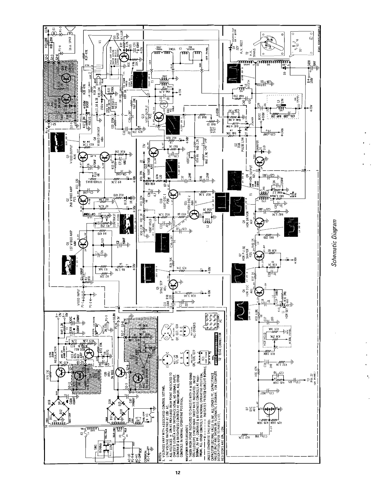
Schematic Diagram
rer no asr-no| ae pees
DIODES & RECTIFIERS
Co) 488134927 D2 488134978 48067120411 D4 488137114 48319105 488137469 488134917 48867120411 48819110 48819110 488191019 488191410 48D67120A11 48819105 48S191A05 48S191A05 488191 A05 48D67120A11 4881064143 488191405 48$191A05
658139424 658139424 658139551
INTEGRATED CIRCUITS
ter 51810732401
COILS & CHOKES
La 24068822008 2 24D68801A67 LS 24069163418 4 2425000074 Ls 2425261403 24D25261A04
TRANSISTORS
488137171 488137127 488134919 488137317 488137115, 488137172 488137127 488137093 488137570 488137173 4gsi37171 488137115 488137596 488134952 488137574 488137368 488137172 488137168 483137769 49s197344 488137476
CONTROLS
RS 18025212409 R10 1802524504 RA7 18C25218A10 R21 18025212410 R34 18025212412 R59 18025245A04 R65 18025245419 R74 18C25218A13 R82 18025212A11 R85 1802521209 REPLACEMENT PARTS LIST
DIODE, Silicon: 010; Damper RECTIFIER, H.V.: Silicon; D2Y
DIODE; Silicon: _D1K; Pulse Limiter DIODE, Low Power
RECTIFIER, Silicon: 91405 DIODE, Silicon: zener; D7G DIODE, Dual: D1¢; Detector DIODE, Low Power RECTIFIER, Silicon: 91410 RECTIFIER, : Q1A10 91A10 RECTIFIER, STA1O DIODE, Low Pe RECTIFIER, Silicon: 91405
RECTIFIER, Silicon: 91A05
DIODE, Low Power
RECTIFIER, Silicon: 91A05 DIODE, Sificon Zener, 04.3
RECTIFIER, Sticon: 91A05
INTEGRATED CIRCUIT: T3F
HORIZSET COMPENSATING: 2000 un HORIZ LINEARITY HORIZ WIDTH: incis C42 & R68 DEFLECTION YOKE XM701-10 DEFLECTION YOKE XM501-10
ist VIDEO: AGH 2nd VIDEO: P25 VIDEO OUTPUT: AIM VIDEO DRIVER: ABH SYNC SEPARATOR: ASU HORIZ OSCILLATOR: A6J HORIZ PULSE SHAPER: P25 HORIZ DRIVER: A5F HORIZ OUTPUT: B2L VERT OSCILLATOR (1): P2W VERT OSCILLATOR (2): AGH VERT DRIVER: ASU VERT OUTPUT: B2V REGULATOR DRIVER; A2J REFERENCE AMP: B2N REGULATOR: A8sW AUDIO DRIVER: A6s AUDIO OUTPUT: P2V 5V REGULATOR, Driv BV REGULATOR: ABU SPOT KILLER: B1E
CONTRAST: 250 Ohm VIDEO BIAS: 4k FOCUS: 2 meg BRIGHTNESS: 200K HORIZ HOLI VERT LINEARITY: 4k VERT SIZE: 100K Ohm REGULATOR ADJUST: 2K. VERT HOLD: 3K VOLUME: 250 0hm RESISTORS
17810130807 178744356 17810130691 178647132
178138589 6810201404
SWITCHES
swt 4081062407
TRANSFORMERS
mW 2552522105 12 24025240007 3 25025221407 14 25025239407 Part of CRT socket assembly Part of CRT socket assembly Part of CRT socket assembly 1500 10% 3W fxd mtl fim 2.2 10% 2w WwW 10 10% 1/2W (special) 1200 10% SW WW (Use 178136197) 150 10% 10W WW VARISTOR Part of CRT Socket
SWITCH, Slide: DPDT (115V — 230V)
HORIZ DRIVER H.V. TRANSFORMER: complete VERT OUTPUT POWER
MISCELLANEOUS ELECTRICAL PARTS
va J9VARP4 22VATP4 50D68384A02 e4 688139451
MECHANICAL PARTS
9066133428
42825158801 31070080604
18810390806
15510183469
s9s10184063
3910184022 15S10630A02 7810609A03 26C66745A05 26C25198A01 9510783A01 140862363
28810733401 287081 551028103 47066082403 35136050
9810143041 9025282A08 9025201401
9C63825A03 96382502 4165987401 66P 65173447 CRT (XM5O1-10 19VP111) CRT (XM701-10 23VP111) SPEAKER: 4” PM LAMP: No, 1436
CAP, SS Rect (HV Transformer — PRI/SEC lead) CLAMP, Metal: Defi Yoke Mtg CONNECTOR, PC panel: 9 contact; ‘on chassis CONNECTOR, PC panel: 12 contact; less key and contacts (power-audio panel) CONNECTOR, Plug: 12 contact; less ‘contacts (power) CONTACT, Plug: for power connector 15S19183A69 CONTACT: for $2 connector COVER, nylon: slide switch; SW1 GROMMET, Plastic: PC panei mtg HEAT SINK: 03 HEAT SINK: Q20 HOLDER, Fuse: F1 & F2 INSULATOR, Mica: Transistor socket; Q9, 013, 016 & 020 (Use 744543810) KEY, Plug: ForS2 connector NUT, hex: 3/8-32; control mtg RIVET, drive pin: nyion; HV transf mtg ROD, Adjustment: width coil; L4 ‘SCREW, tpg: 6-20 x 1/2 clu pan hd: Q9, 013, 016 & 020 SOCKET, lamp: E1 SOCKET, CRT: incis leads & resistors SOCKET, HV Rectifier: complete; incls 2nd anode lead & cup SOCKET, transistor: 09,013, 016 SOCKET, transistor: 020 SPRING, special: CRT aquadag gn TOOL, contact removal (S2 connector)