Millipede SP-217 1st Printing
Millipede (Atari, 1982) · Schematic Package · 15 pages · 45 sections · original scan
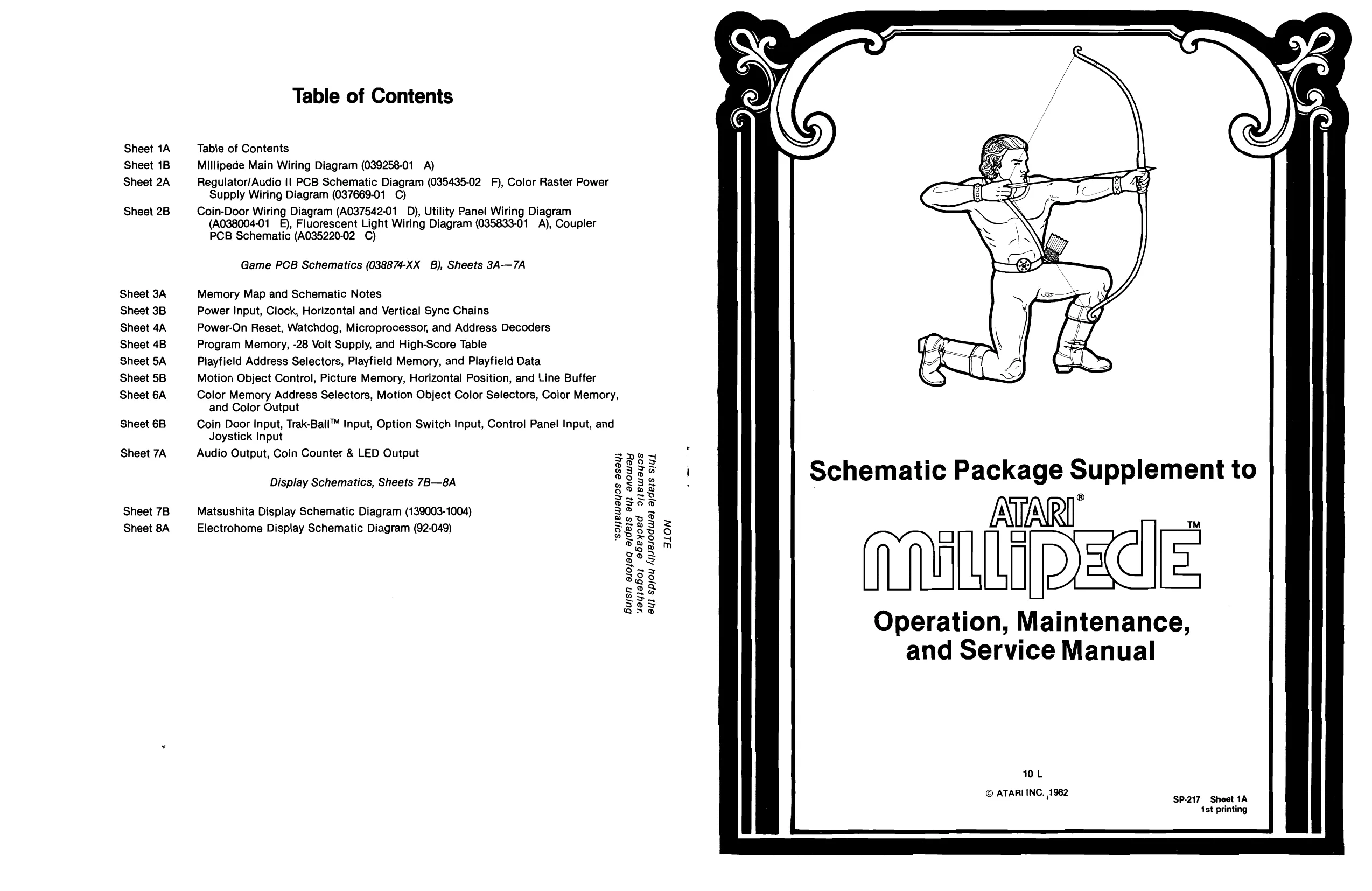
Table of Contents
Sheet 1A Table of Contents Sheet 1B Millipede Main Wiring Diagram (039258-01 A) Sheet 2A Regulator/Audio || PCB Schematic Diagram (035435-02 F), Color Raster Power Supply Wiring Diagram (037669-01 C) Sheet 2B Coin-Door Wiring Diagram (A037542-01 D), Utility Panel Wiring Diagram (A038004-01 £), Fluorescent Light Wiring Diagram (035833-01 A), Coupler PCB Schematic (A035220-02 C)
Game PCB Schematics (038874-XX B), Sheets 3A—7A
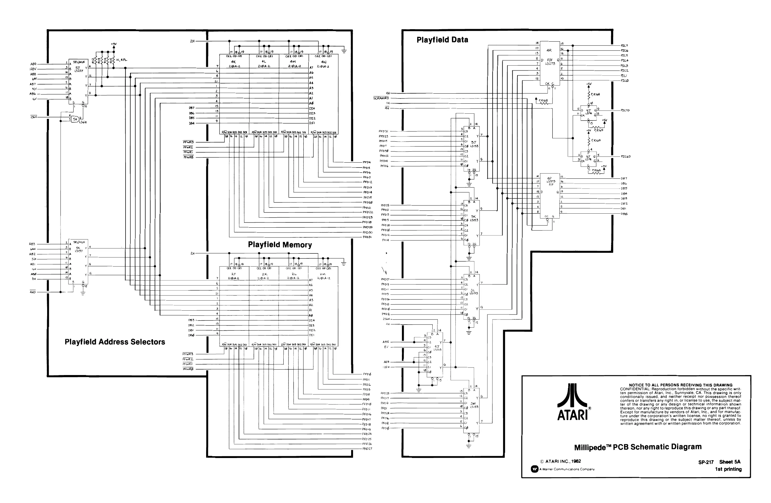
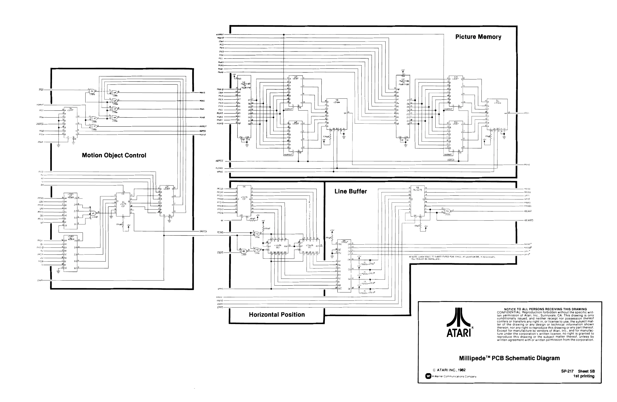
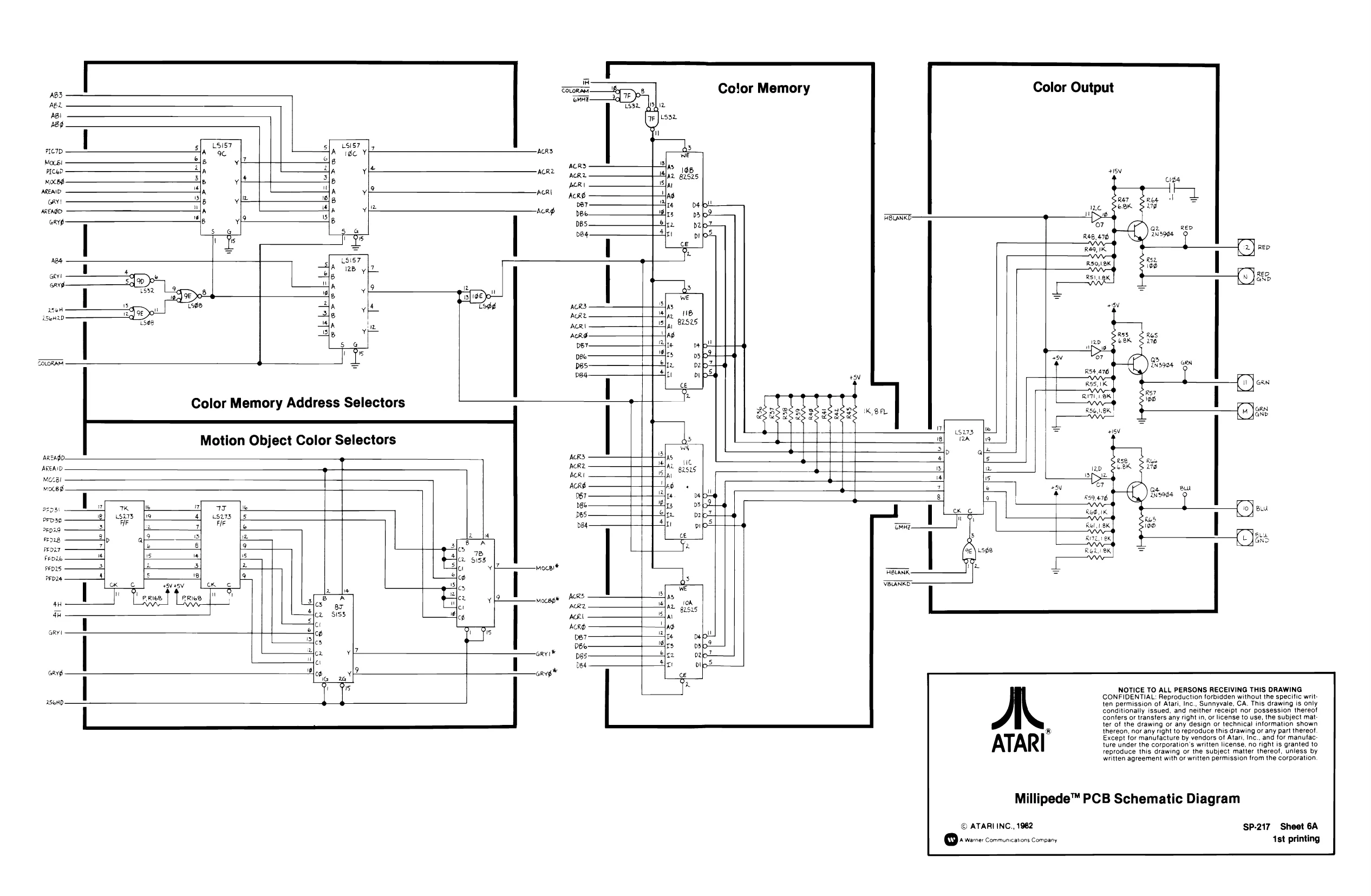
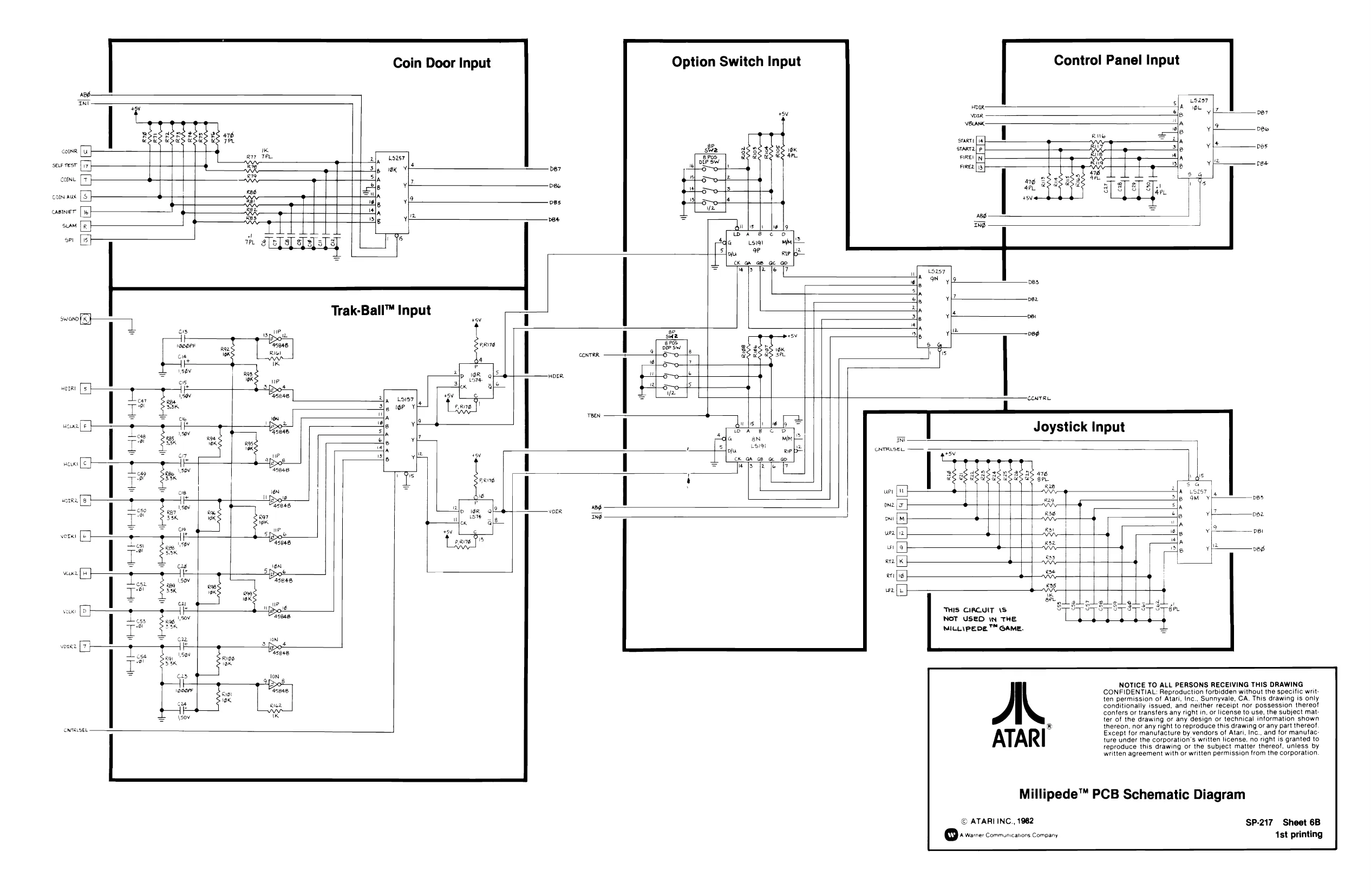
Sheet 3A Memory Map and Schematic Notes Sheet 3B Power Input, Clock, Horizontal and Vertical Sync Chains Sheet 4A Power-On Reset, Watchdog, Microprocessor, and Address Decoders Sheet 4B Program Memory, -28 Volt Supply, and High-Score Table Sheet 5A Playfield Address Selectors, Playfield Memory, and Playfield Data Sheet 5B Motion Object Control, Picture Memory, Horizontal Position, and Line Buffer Sheet 6A Color Memory Address Selectors, Motion Object Color Selectors, Color Memory, and Color Output Sheet 6B Coin Door Input, Trak-Ball™ Input, Option Switch Input, Control Panel Input, and Joystick Input Sheet 7A Audio Output, Coin Counter & LED Output Schematic Package Supplement to ATARY i
Operation, Maintenance, and Service Manual Display Schematics, Sheets 7B—8A
Sheet 7B Matsushita Display Schematic Diagram (139003-1004) Sheet 8A Electrohome Display Schematic Diagram (92-049) “soyjewayos asay) Bujsn asojaq ajdeis ay} anoway 4yayja6o0} abeyoed oiewayos ay} spjoy Ajjsesodusa} ajdeys siyt
JLON
10L
© ATARI ING. 1982 SP-217 Sheet 1A 1st printing
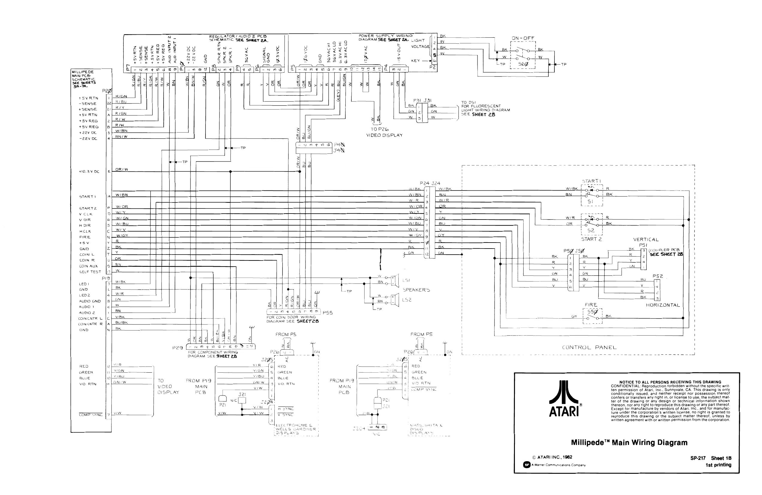
This page is a drawing, shown as the original scan.
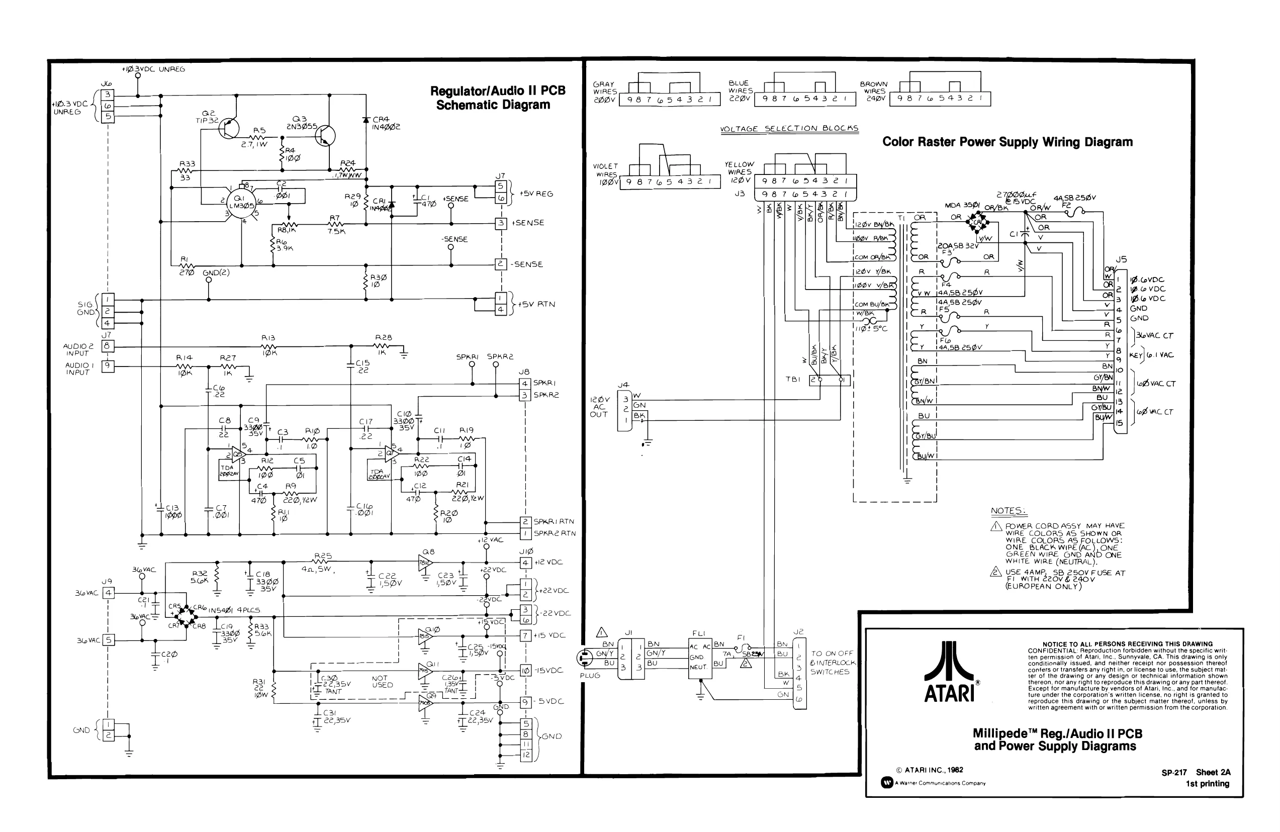
This page is a drawing, shown as the original scan.
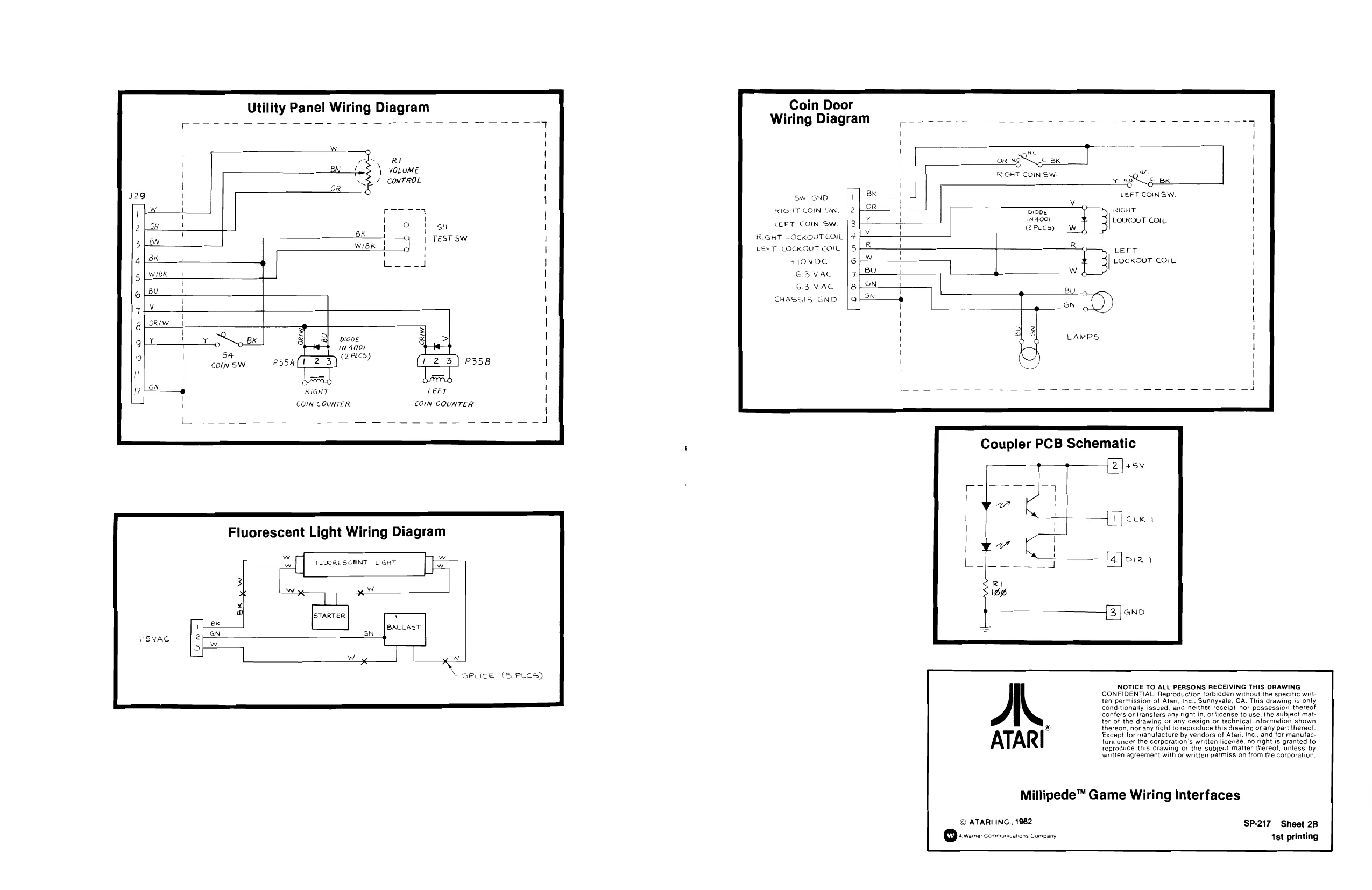
Coin Door
Wiring Diagram
RIGHT COIN SW.
Sw. GND 4+ LEFT COINSW,
| RIGHT COIN SW. | 2 | TT | DIODE, | RIGHT | |
| E | p___I | iN 4001 | LOCKOUT COIL | |
| sit | LEFT COIN SW. | (pies) | W | | |
TEST SW RIGHT LOCKOUT COIL LEFT LOCKOUT COIL, LEFT +1OVDC t | LOCKOUT COIL 63 VAC w
6.3 VAC S
1 pu CHASSIS GND 20) on y,
ioe | 2] a| 3
1 4001 (2PLcs) LAMPS
RIGHT
COIN COUNTER
4+5V
Fluorescent Light Wiring Diagram
W FLUORESCENT LIGHT
x
STARTER T
BALLAST NSVAC o
w
- * \ spice (5 PLCs) NOTICE TO ALL PERSONS RECEIVING THIS DRAWING CONFIDENTIAL: Reproduction forbidden without the specific writ: ten permission of Atari, Inc.. Sunnyvale, CA. This drawing is only conditionally issued, and neither receipt nor possession thereot
confers or transfers any right in, or license to use, the subject mat
ter of the drawing or any design or technical information shown ® thereon, nor any right to reproduce this drawing of any part thereof Except for manufacture by vendors of Atari. Inc., and for manutac: ture under the corporation's written license. no right is granted to reproduce this drawing or the subject matter thereof, unless by waitten agreement with or written permission from the corporation.
Millipede™ Game Wiring Interfaces
SP-217 Sheet 2B 1st printing
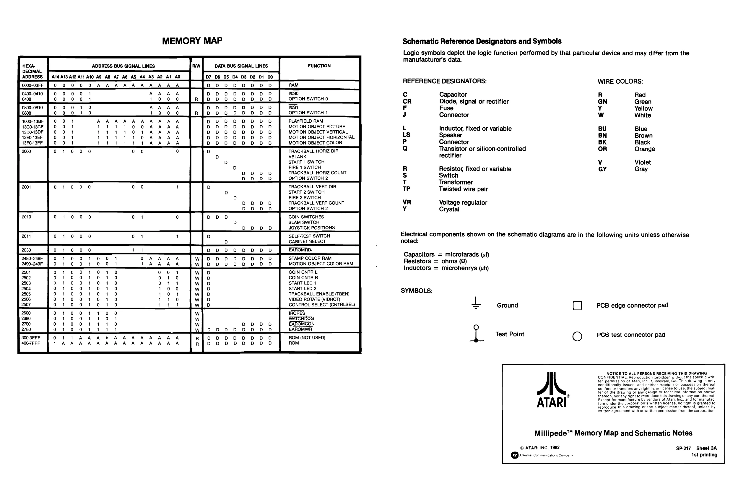
1000-13BF 13C0-13CF 13D0-13DF 13E0-13EF 13FO-13FF
MEMORY MAP
DATA BUS SIGNAL LINES
D7_D6 D5 D4 D3 D2 Di DO D DDD io) DDD
- OD DD D DDD } DD OD fe) DDD D DoDoD fe) DDD D DDD D D DOD loofoo loo fo D
D D
D oD
fe) D D D [e) oo0000fo00 fon fo
°
° DD DoD i cofo solo oofo ooo solo colo colo oo0co00]|00
(xe) oofo oofo ooo oofo oo oofoo gofoo oofoo | 0 DOD Do oD
w Ww
w w w w w w Ww
Ww w w w FUNCTION
OPTION SWITCH 0
ost OPTION SWITCH 1
PLAYFIELD RAM MOTION OBJECT PICTURE MOTION OBJECT VERTICAL MOTION OBJECT HORIZONTAL MOTION OBJECT COLOR
TRACKBALL HORIZ DIR VBLANK START 1 SWITCH FIRE 1 SWITCH TRACKBALL HORIZ COUNT OPTION SWITCH 2
TRACKBALL VERT DIR ‘START 2 SWITCH FIRE 2 SWITCH TRACKBALL VERT COUNT OPTION SWITCH 2
COIN SWITCHES ‘SLAM SWITCH JOYSTICK POSITIONS
SELF-TEST SWITCH CABINET SELECT
EAROMRD-
STAMP COLOR RAM MOTION OBJECT COLOR RAM
COIN CNTR L COIN CNTR R START LED 1 START LED 2 TRACKBALL ENABLE (TBEN) VIDEO ROTATE (VIDROT) CONTROL SELECT (CNTRLSEL)
ROM (NOT USED) ROM
Schematic Reterence Designators and Symbols
Logic symbols depict the logic function performed by that particular device and may differ from the manufacturer's data.
REFERENCE DESIGNATORS:
Cc Capacitor
CR Diode, signal or rectifier Fuse J Connector
L Inductor, fixed or variable Ls Speaker P Connector
Qa Transistor or silicon-controlled
rectifier
R Resistor, fixed or variable s Switch T Transformer
TT Twisted wire pair
VR Voltage regulator Y Crystal WIRE COLORS:
R Red GN Green Y Yellow
Ww White
BU Blue BN Brown BK Black OR Orange
Vv Violet GY Gray
Electrical components shown on the schematic diagrams are in the following units unless otherwise noted:
Capacitors = microfarads (uf) Resistors = ohms (Q) Inductors = microhenrys (uh)
SYMBOLS: L Ground
A. ATARI PCB edge connector pad
PCB test connector pad
NOTICE TO ALL PERSONS RECEIVING THIS DRAWING CONFIDENTIAL: Reproduction forbidden without the specific writ: ten permission of Atari, Inc., Sunnyvale, CA. This drawing is only conditionally issued, and neither receipt nor possession thereof confers or transfers any right in, or license to use, the subject mat ter of the drawing or any design or technical information shown thereon, nor any right to reproduce this drawing or any part thereof Except for manufacture by vendors of Atari, Inc., and for manufac: ture under the corporation's written license, no right is granted to reproduce this drawing or the subject matter thereof, unless by written agreement with or written permission from the corporation.
Millipede™ Memory Map and Schematic Notes
SP-217 Sheet 3A 1st printing
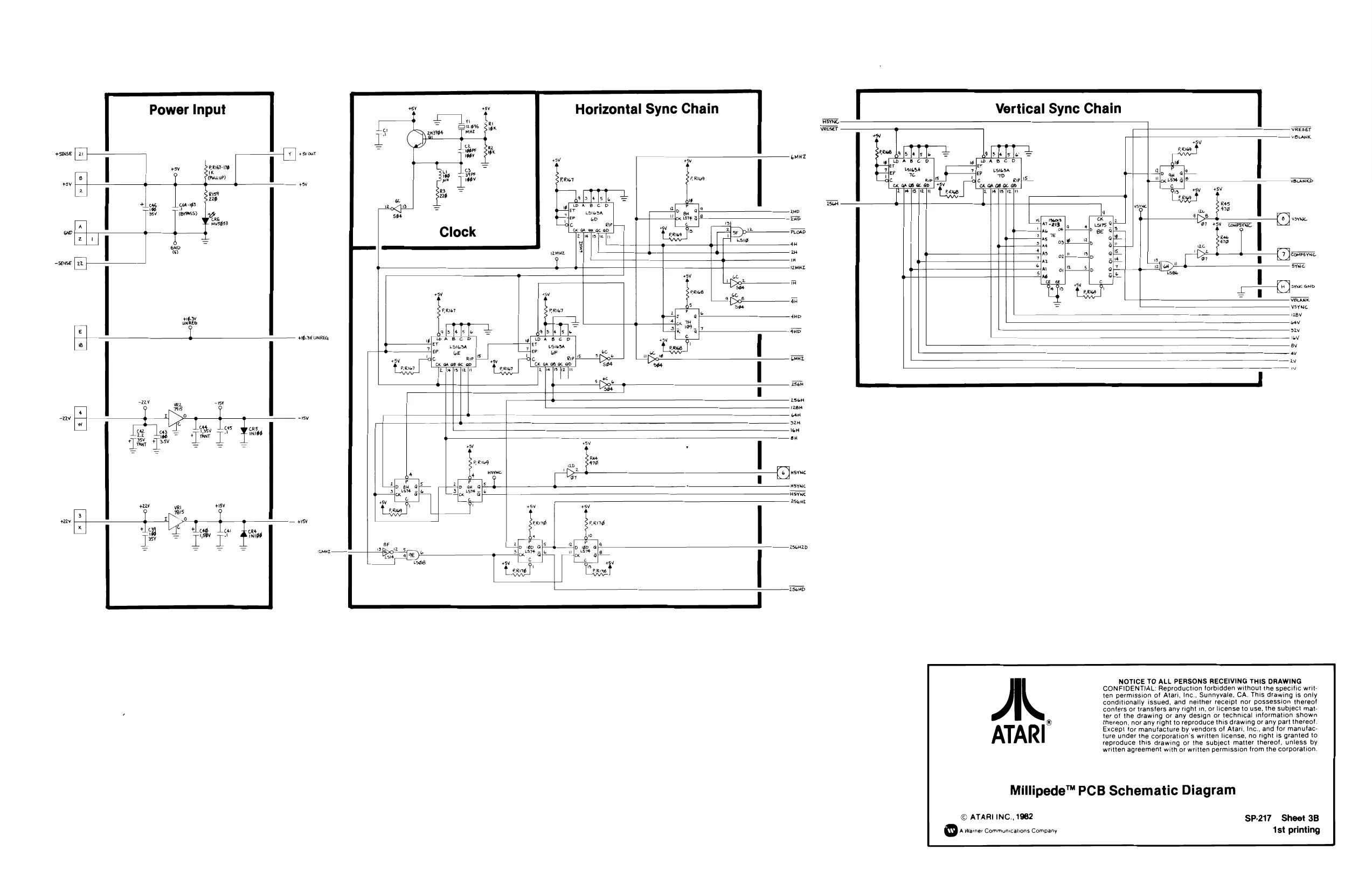
Horizontal Sync Chain
Power Input
Vertical Sync Chain
vaeset
S056 oun
ma
a 7 vec, oo FOR z[0 4K as — al oman wsene fit ” awn ame
a cord Verne ano sy
a cod 2av e ev
ome Ww
mm
ren rn rae aw can w 22H eH oH
Bloc
neni
25eut
ad
2542p
roy
NOTICE TO ALL PERSONS RECEIVING THIS DRAWING CONFIDENTIAL: Reproduction forbidden without the specific writ: ten permission of Atari, Inc., Sunnyvale, CA. This drawing is only conditionally issued, and neither receipt nor possession thereot : confers or transfers any right in, or license to use, the subject mat. ter of the drawing or any design or technical information shown thereon. nor any right to reproduce this drawing or any part thereot Except for manufacture by vendors of Atari, Inc., and for manufac: ture under the corporation's written license, no right is granted to reproduce this drawing or the subject matter thereof, unless by written agreement with or written permission from the corporation.
Millipede™ PCB Schematic Diagram
© ATARI INC., 1982 SP-217 Sheet 3B QD A vere: Communications Company 1st printing
This page is a drawing, shown as the original scan.
oon Lt Jo ve we Veep | Yep Bee a Iq SP
asi
es.
ne
28s Mt
las
ast
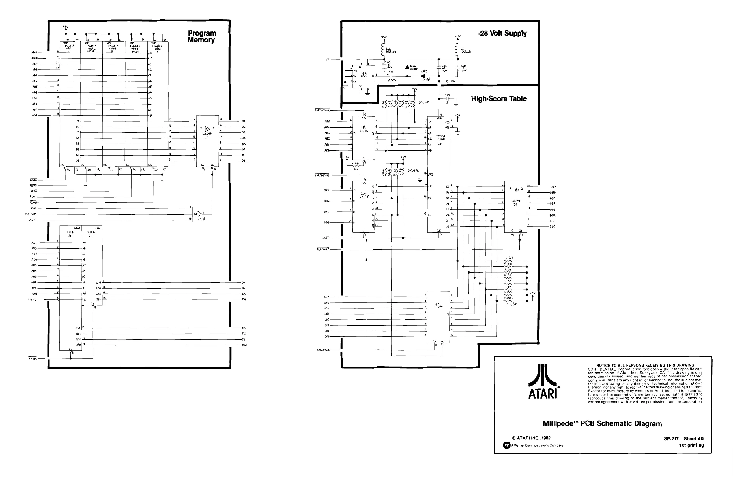
ne lag Program Memory
Ls2ee eo] ir |e
les les cs. | hey
isig
aut ar mM cry Paes
AB.
ass:
ABs —
nes
yen.
ast aos ang. Asn
Tae Ho! b ROR.
as
Ae: ABs. >
3 2 WP dep uf Is.
Ries iene! ‘Dd -28 Volt Supply
High-Score Table
ors ABY
pez
le a] bstas 3 et
ved plo ooo
cord
Re.
NOTICE TO ALL PERSONS RECEIVING THIS DRAWING CONFIDENTIAL: Reproduction forbidden without the specitic writ ten permission of Atari, Inc., Sunnyvale, CA. This drawing is only conditionally issued, and neither receipt nor possession thereot coniers or transfers any right in, or license to use, the subject mat ter of the drawing or any design oF technical iniormation shown thereon, nor any right to reproduce this drawing or any part thereo! Except for manufacture by vendors of Atari, Inc., and for manufac ture under the corporation's written license, no right is granted to reproduce this drawing or the subject matter thereof, unless by written agreement with or written permission trom the corporation,
ATARI
Millipede™ PCB Schematic Diagram
SP-217 Sheet 4B Ast printing
This page is a drawing, shown as the original scan.
This page is a drawing, shown as the original scan.
This page is a drawing, shown as the original scan.
This page is a drawing, shown as the original scan.
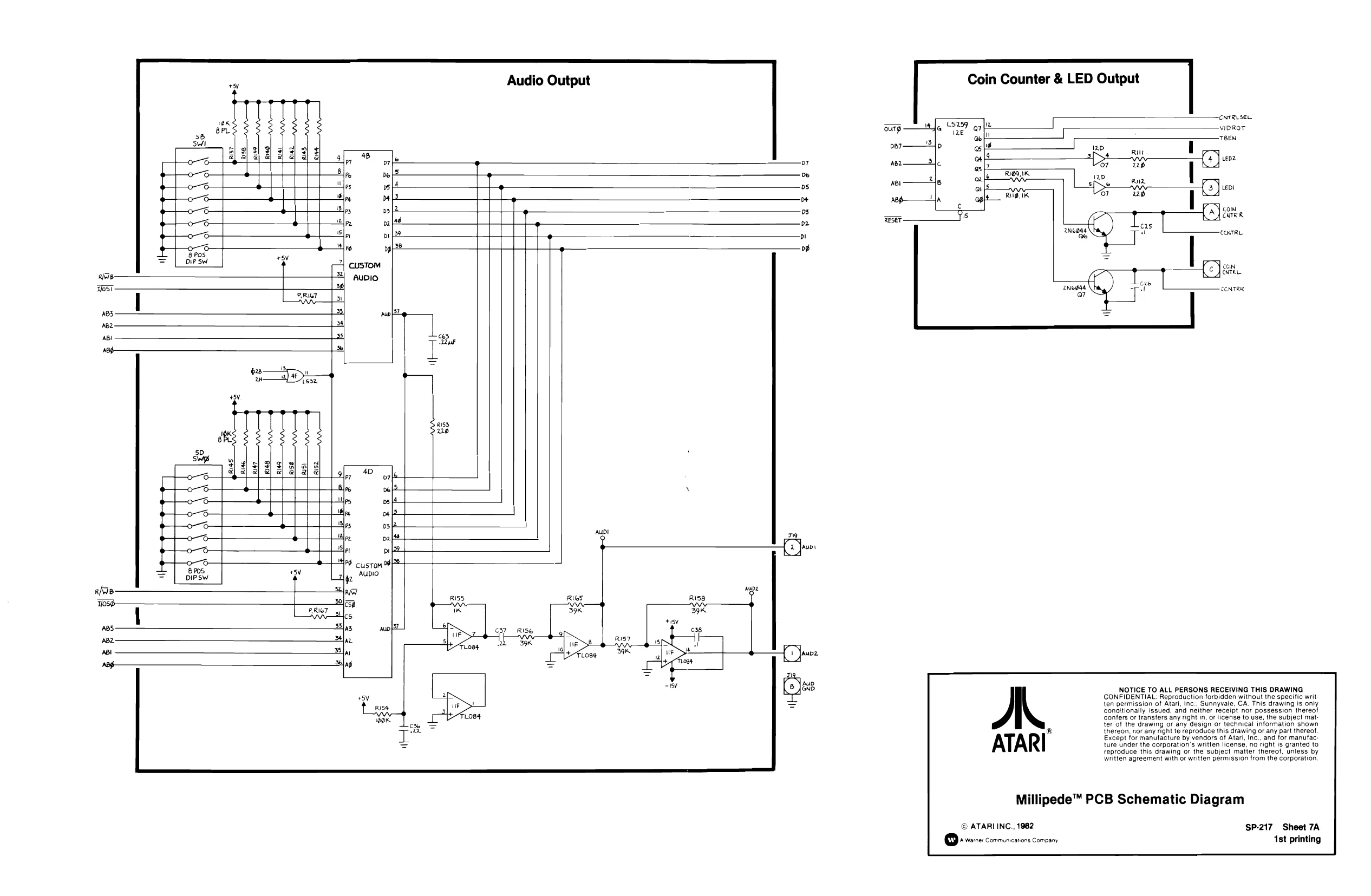
This page is a drawing, shown as the original scan.
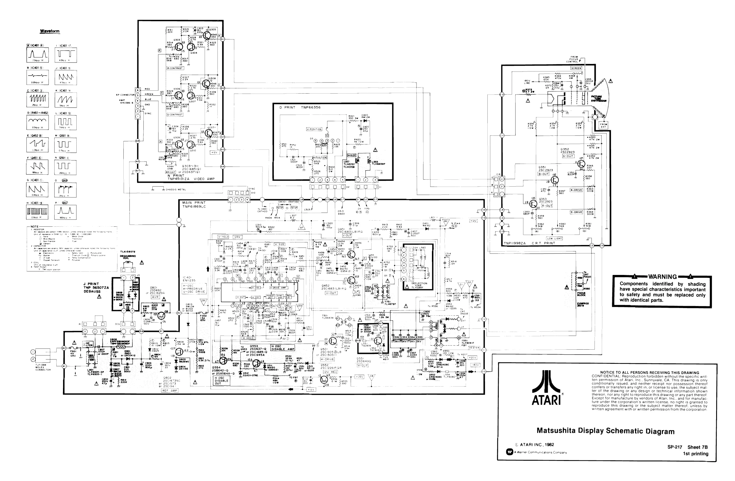
This page is a drawing, shown as the original scan.
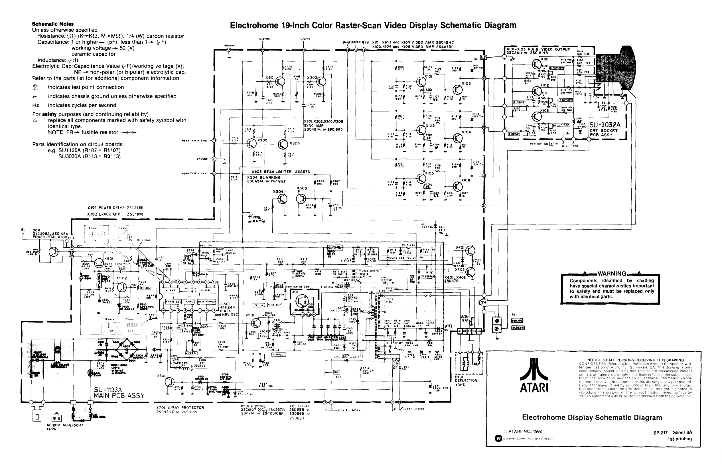
Groomers seated Electrohome 19-Inch Color Raster-Scan Video Display Schematic Diagram Resistance: (Q) (K-*KQ., MMQ), 1/4 (W) carbon resistor ssene sew Capacitance: 1 or higher-» (pF), less than 1-> (yF) anouno Biug aneeN RED X101.X1O3 and XI0S VIDEO AMP. 28C454C working voltage —» 50 (V) —— \ X102.x104 and Xi06 VIDEO AMP. 25A673C Ts Poa] IRE outa ad re ceramic capacitor SC2GEII or ZSCISI4 \nductance: (»H) Electrolytic Cap: Capacitance Value ( F)/working voltage (V), NP -+ non-polar (or bipolar) electrolytic cap. Refer to the parts list for additional component information 2 indicates test point connection au ah indicates chassis ground unless otherwise specified ae Hz indicates cycles per second For safety purposes (and continuing reliability) a replace all components marked with safety synbol with ' 301, 302, X308,X308.
identical type. SYNC SU-3032A
X3O3 BEAM LIMITER 2SA673 pin [2304 BLANKING 2SCARAC oF BSC/6Es wees tive v. syne 1
x304
X901 POWER DRIVE 252688 X902 ERROR AMP = 2SC 1890 —— ee
Bovoes 281454 REGU GULATOR so.
eae or 3.5808 pia
maa? D506 woe ia af eae ny e817 18/6} Ed 60 ~ = P1383 [asic 6s w cur evo vin ihe — masta Pera.
geo, oben
NOTICE TO ALL PERSONS RECEIVING THIS DRAWING
CONFIDENTIAL. Reproduction forbidden without tne specific writ
ten permission of Atari, Inc., Sunnyvale, CA, This drawing IS only canditionally issued, and neither receipt nor possession thereo! baeente conters oF transfers any right in, or license to use, the subject rat ter of ine drawing or any design ar technical information shown
DEFLECTION ny right 10 reproduce this drawing of any part tnereot
YOKE, mufacture by vendors ot Atari. Inc. and for manufac. e corporation's whiten license. no right is granted to ject matter thereat, unless by written agreement with or written permission from the corporation SU-1133A fe 9305 MAIN PCB ASSY :
2SC454C or 2SC1685 2SC26ll of 2SC2610BK 250869 or cx on 250820 a
Electrohome Display Schematic Diagram
ACIZ0V 6OHz/SoHZ acizo © ATARIINC,, 1982 SP-217 Sheet 8A oO: warner Communications Compa 4st printing