Paperboy TM-275 1st Printing
Paperboy (rev 3) (Atari Games, 1984) · Technical Manual · 100 pages · 92 sections · original scan
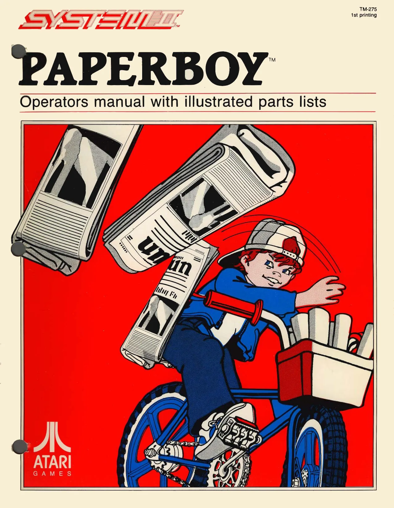
This page is a drawing, shown as the original scan.
Atari Games Corporation Customer Service
If reading through this manual does not lead to solving a certain maintenance problem, call TELEHELP® at one of these Atari Games Customer Service offices:
UNITED STATES
Parts and Service
California Customer Service Office 737 Sycamore Drive P.O. Box 361110 Milpitas, CA 95035-1110 Telex 17-2976 (Monday-Friday, 7:30-4:00 pm Pacific Time) s (408) 434-3950
EUROPE
Parts and Service
European Customer Service Office Tipperary Town, Ireland Telex 28165 (Monday-Friday, 9:00-6:00 pm GMT) s 062-52155
E BOY PA
Operators manual with illustrated parts lists
© 1985 by Atari Games Corporation All rights reserved. No part of this publication may be reproduced by any mechanical, photographic, or electronic process, or in the form of aphonographic recording, nor may it be stored in a retrieval system, transmitted, or otherwise copied for public or private use, without permission from the publisher. The game play, all graphic designs, this technical manual, its accompanying schematic diagrams, and the display manual are protected by the U.S. Copyright Act of 1976. This Act provides for increased penalties for violating federal copyright laws. Courts can impound infringing articles while legal action is pending. If infringers are convicted, courts can order destruction of the infringing articles. In addition, the Act provides for payment of statutory damages of up to $250,000 in certain cases. Infringers may also have to pay costs and attorneys’ fees and face an imprisonment of up to five years. Atari Games Corporation will aggressively enforce its copyrights against any infringers. We will use all legal means to immediately halt any manufacture, distribution, or operation of acopy of video games made by us, Anyone who purchases such copies risks forfeiting such a game.
Published by: Atari Games Corporation 1272 Borregas Avenue P.O. Box 3618 Sunnyvale, California 94088
Printed in the U.S.A. 1P
Notice Regarding Non-ATARI Parts
Use of non-ATARI® parts or modifications of any ATARI game circuitry may adversely affect the safety of your game, and may cause injury to you and your players.
You may void the game warranty (printed on the inside back cover of this manual) if you do any of the following: © Substitute non-ATAR! parts in the game.
- Modify or alter any circuits in the game by using kits or parts not supplied by Atari Games Corporation.
NOTE
This equipment generates, uses, and can radiate radio frequency energy and if not installed and used in accordance with the instruction manual, may cause interference to radio communications. It has been tested and found to comply with the limits for a Class A computing device pursuant to SubpartJ of Part 15 of Federal Communications Commission (FCC) Rules, which are designed to provide reasonable protection against such interference when operated in a commercial environment. Operation of this equipment in a residential area or modification to this equipment is likely to cause interference in which case the user, at his own expense, will be required to take whatever measures may be required to correct the interference. if you suspect interference from an ATARI® game at your location, check the following: © All green ground wires in the game are properly connected as shown in the game wiring diagram. © The power cord is properly plugged into a grounded three-wire outlet. © The game printed-circuit boards (PCB) are properly installed with the Electromagnetic Interference (EM!) ground plane. If you are still unable to solve the interference problem, please contact Customer Service at Atari Games Corporation. See the inside front cover of this manual for service in your area,
iii
Table of Contents
Set- How to Use This Manual Inspecting the Game... Control and Switch Locations. Coin and Game Option Settings . Operating Modes. Game Play... Operator Hints .
Self-Test RAM/InterrupUROM Test 6502 Processor Test. Control Test 2.0... Calibration Procedure Alphanumeric Tes‘.. Scrolling Playfield Tes Motion Object Test. Mouton Object Height Test Color Bar Test. 25 Color Purity Test . 2-6 Convergence Test 26 Accounting Information 2-6 Switch Settings . 2-7 Maintenance Preventive Maintenance ..... Preventive-Maintenance Intervals Removing the Contro! Panel .. Lubricating and Tightening the Handlebar Control Cleaning the Coin Mechanism .. Cleaning the Interior Components . PP e eww SRRROK
rs Corrective Maintenance... Removing the Video Display Removing the Game PCBs Removing the Fluorescent-Light Assembly .. Removing the Speakers .... Disassembling the Handlebar Control : Aligning the Handlebar Control Potentiometers. Calibrating the Handlebar Control...
Troubleshooting Troubleshooting Procedures Troubleshooting Techniques Soldering Techniques........ Troubleshooting Static-Sensitive Device:
Illustrated Parts List See List of Illustrations on next page.
Appendix: Installation Kit Parts Inventory Tools Required .... Installation Instructions . Setting the Coin and Game Options. AnwoyaAd yy Paperboy
Paperboy
List of Illustrations
Figure 1-1 Figure 1-2 Figure 2-1 Figure 2-2 Figure 2-3 Figure 2-4 Figure 2-5 Figure 2-6 Figure 2-7 Figure 2-8 Figure 2-9 Figure 2-10 Figure 2-11 Figure 2-12 Figure 2-13 Figure 2-14 Figure 2-15, Figure 2-16 Figure 2-17 Figure 2-18
Figure 3-1 Figure 3-2 Figure 3-3 Figure 3-4 Figure 3-5 Figure 3-6 Figure 3-7 Figure 3-8 Figure 3.9
Figure 4-1 Figure 4-2 Figure 4-3 Figure 4-4
Figure 5-1 Figure 5-2 Figure 5-3 Figure 5-4 Figure 5-5 Figure 5-6 Figure 5-7 Figure 5-8 Figure 5-9 Figure 5-10 Figure 5-11 Figure 5-12
Figure A-1 Figure A-2 Figure A-3 Figure A-4 Figure A-5
‘Table 1-1 Table 1-2 Table 1-3 Table A-1 Game Overview .. Control and Switch Locations . RAM Test Fails . Interrupt ‘Test Fails... ROM Test Fail: Reset Retry........ Communications Fails Music/RAM/ROM Fails Sound Output... Sound Status Control Test Passes. Alphanumeric Test . Scrolling Playfield Test Motion Object Test . Motion Object Height Test Color Bar Test... Coler Purity Test. Convergence Test Accounting information Switch Settings. be
DWaar bh bh ROW oa
Control Panel Removal Video Display Removal Game PCB Removal... Fluorescent-Light Assembly ‘Removal Speaker Removal .. . Handlebar Control Removal ‘Torsion Spring and Modification Bearing Installation. Accelerator Unit Disassembly/Reassembly Steering Unit Disassembly/Reassembly ..
Removing IC (Cut-Pin Method) Removing IC Pins .. Removing Solder from Plated” ‘Through Holes Removing Solder from Lead Connection Pads. wBHeSoemAbke UB
An RRO
Cabinet-Mounted Assemblies Control Panel Assembly ... Handlebar Control Assembly Fluorescent Tube Assembly Power Supply Assembly. Utility Panel Assembly... . Coin Controls, Inc. Coin Door Assembiy Coin Acceptors, Inc. Coin Door Assembly Printed-Circuit Board Mounting Hardware ... Central Processing Unit PCB Assemb! 5-22 Video PCB Assembly... 530 Regulator/Audio UI PCB Assembl 5-38
Kit Part Locations.. : A2 Attraction Film Replacement A-4 Control Panel Replacement... A4 Video Display Removal and Repacenent AS5 Game ROM Replacement .. AT
List of Tables
Game Specifications 12 Coin and Credit Settings. 15 Game Option Settings . 15 Kit Parts Inventory........ A3
vii
Safety Summary
The following safety precautions apply to al! game operators and service personnel. Specific warnings and cautions will be found throughout this manual where they apply.
A WARNING A
Properly Ground the Game. Players may receive an electrical shock if this game is not properly grounded! To avoid electrical shock, do not plug in the game until it has been inspected and properly grounded. This game should only be plugged into a grounded threewire outlet. if you have only a two-wire outlet, we recommend you hire a licensed electrician to install a grounded outlet. Players may receive an electrical shock if the control panel is not properly grounded! After servicing any parts on the control panel, check that the grounding clip is firmly secured to the metal tab on the inside of the control panel. Only then should you lock up the game AC Power Connection. Before connecting the game to the AC power source, verify that the proper voltage-selection plug is installed on the game’s power supply. Disconnect Power During Repairs. To avoid electrical shock, disconnect the game from the AC power source before removing or repairing any part of the game. When removing or repairing the video display, extra precautions must be taken to avoid electical shock because high voltages may exist within the display circuitry and cathode-ray tube (CRT) even after power has been disconnected. Do not touch internal parts of the display with your hands or with metal objects! Always discharge the high voltage from the CRT before servicing this area of the game. To discharge the CRT: Attach one end of a large, wellinsulated, 18-gauge jumper wire to ground. Momentarily touch the free end of the grounded jumper to the CRT anode by sliding it under the anode cap. Wait two minutes and discharge the anode again. Use Only ATARI Parts. To maintain the safety integrity of your ATARI game, do not use non-ATARI parts when repairing the game. Use of non-ATARI parts or other modifications to the game circuitry may adversely affect the safety of your game, and injure you or your players. Handle Fluorescent Tube and CRY With Care. If you drop a fluorescent tube or CRT and it breaks, it may implode! Shattered glass can fly six feet or more from the implosion. Use the Proper Fuses. To avoid electrical shock, use replacement fuses which are specified in the parts list for this game. Replacement fuses must match those replaced in fuse type, voltage rating, and Current rating. In addition, the fuse cover must be in place during game operation,
Set-Up
How to Use This Manual
Your System II™ cabinet is designed to be used for a variety of games. The System II cabinet comes with a System II game installed at the factory or, if you already have a System II game, any available System II game can be purchased as a kit for easy installation. This operators manual is for the PRPERBOY™ game, and is supplied either with System II cabinets that have the PAPERBOY game installed at the factory or with PAPERBOY kits that can be installed in the field. This manual includes information for setting up, playing, and maintaining your System II PAPERBOY game. If you have purchased a PAPERBOY kit to change an existing System II game into a PAPERBOY game, the Appendix of this manual contains all the necessary information for installing the PAPERBOY game kit. This manual is divided into the following chapters: © Chapter | contains set-up information. © Chapter 2 contains self-test procedures. © Chapter 3 contains preventive and corrective maintemance procedures, Chapter 4 contains troubleshooting information. Chapter 5 contains illustrated parts lists. © The Appendix contains procedures for installing the PAPERBOY kit. Schematic diagrams for the System II] PAPERBOY game circuitry are in the SP-275 Schematic Package Supplement included with this manual. This chapter includes information required to set up and play your PAPERBOY game. Carefully read the information in this chapter before applying power to the game. To avoid electrical shock, do not plug in the game until it has been properly inspected and set up for the line voltage in your area. This game should only be connected to a grounded three-wire outlet. If you have only a two-wire outlet, we recommend you hire a licensed electrician to install a grounded outlet. Players may receive an electrical shock if the game is not properly grounded. Do not touch internal parts of the display with your hands or with metal objects.
Chapter 1
setup
Inspecting the Game
Do not plug in the game unti] you have completed the following factory-assembled game or kit inspection steps.
Please inspect your System I] PAPERBOY game (or kit) carefully to ensure that the game (or kit) is complete and delivered to you in good condition. Figure 1-1 shows the locations of the component parts of the assembled game. Refer to Appendix A for a list of che kit parts. Table 1-1 lists space, power, and environmental requirements.
Inspect the factory-assembled game as follows:
- Examine the exterior of the cabinet for dents, chips, or broken parts.
- Unlock and open the rear-access door Unlock and open the coin doors. Inspect the interior of the cabinet as follows:
a. Ensure that all piug-in connectors (on the cabinet harnesses} are firmly plugged in. Do not force connectors together. The connectors are keyed so they only fit in the proper orientation. 4 reversed edge connector may damage a printed-circuit board (PCB) and wiil void your warranty.
b. Ensure that all plug-in integrated circuits on each PCB are firmly plugged into their sockets.
¢. Inspect the power cord for any cuts or dents in the insulation.
d. Inspect the power supply. Make sure that the correct fuses are installed and that the voltage plugs are inserted for the proper line voltage. Check that the harness is plugged in correctly and that the fuse-block cover is mounted in place, Check that the green ground wire is connected.
e. Inspect other major sub-assemblies, such as the video display, printed-circuit boards (PCBs), speakers, and the fluorescent tube. Make sure they are mounted securely and that the green ground wires are connected.
Inspect the PAPERBOY kit as follows:
- Check that all the PAPERBOY kit parts listed in Appendix A are included in your kit.
- Examine the kit parts for dents, chips, or broken parts. Paperboy
Table 1-1 Game Specifications
Characteristic Specification
315 V-A, 260 W RMS maximum with kit parts installed. +Sto +38 C(+37to +100F) Power Consumption
Temperature Humidity Not to exceed 95% relative Line Voltage 100 to 132 VAC (or 200 to 264 VAC) Width 25.25 in. 64 em) Depth 37 in. (94 cm) Height 72 in. (183 cm) Weight 350 Ibs. (159 kg) maximum with kit parts installed
Control and Switch Locations
Power On/Off Switch The power on/off switch is located at che bottom rear of the cabinet (see Figure 1-1).
Volume Control The volume control is located on the utility panel behind the upper coin door (see Figures 1-1 and 1-2). The volume contro! adjusts the level of sound produced by the game.
Auxiliary Coin Switch
The auxiliary coin switch is located on the coin mechanism.
Coin Counters The coin counter(s) are located on the utility panel behind che upper coin door. The coin counter(s) record the number of coins entered.
Self-Test Switch The self-test switch is located on the utility panel behind the upper coin door. The self-test switch selects the Self Test Mode to check game operation, Refer to Chapter 2 for a complete description of self-test operation.
Coin and Game Option Settings
The System Il cabinet has two dual-in-line package (DIP) option switches located on the CPU printed-circuit board (PCB).
- The option switch at location 6/74 is for selecting coin options. © The option switch at location 5/6A is for selecting game options.
Paperboy set-up
Video Display"
CPU PCB* See Figure 5-10 Fluorescent Light Assy See Figure 5-4
Attraction Panel See Figure 5-1
5V Power Supply” Speaker Grille and Speakers See Figure 5-1
Video PCB* See Figure 5-11
Handlebar Control Assy See Figure 5:3
Utility Panel See Figure 5-6 Control Pane! Assy See Figure 5-2
Regulator/Audio Ill PCB* See Figure 6-12
Power On/Off Switch
AC Power Cord Coin Door See Figures 5.6 and 5-7
Power Supply Assy* See Figure 5-5
“Items with a serial number label
Figure 1-1 Game Overview
SerUp
Coin Counter
Auxiliary Coin Switches Paperboy
Coin Option Switch
CPU PCB
Self-Test Switch
Volume Control
Figure 1-2 Control and Switch Locations
Settings for the PAPERBOY coin and game options are listed in Tables 1-2 and 1-3. Options preset at the factory are shown by the <4 symbol; however, you may change the settings according to your needs. To verify the option selections, check the Switch Setting screen obtained in the Self-Test Mode as described in Chapter 2.
Operating Modes
There are four operating modes for the PAPERBOY game: Attract, Play, High-Score, and Self-Test.
Attract Mode The Attract Mode begins either when the game is plugged in or after exiting the Play, High-Score, or Self-Test Modes. The Attract Mode ends when the correct amount of coins or tokens are inserted and the one- or two-player start (throw) button on the handlebar control is pressed, or when the self-test switch is turned off. The Attract Mode continuously cycles through the following events:
- Title Page—A newspaper page is displayed with the title PAPERBOY and assorted headlines. In the center of the page is a picture of the PAPERBOY. The top three scorers in the Grand Slam table are shown under the titles X.X.X.CHOSEN PAPERBOY OF THE MONTH and X.X.X.,X.X.X.EARN RUNNER UP AWARDS.
- High-Score Table—The four High Score tables are displayed (Easy Street, Middle Road, Hard Way, and Grand. Slam). Scores are highlighted to show the corresponding scores in the street High Score tables and in the Grand Slam table.
Paperboy Set-Up
Table 1-2 Coin and Credit Settings
Settings of 8-Toggle Switch on
4 5 6 Paperboy CPU PCB (at 6/7A) 7 8 Option
Off Off On On off
Off On
Off On
Off Off Off Off On On On off Off On On off Off Oa Off On Off On Off On On Coias Per Credit 1 Coin 1 Credit 2 Coins | Credit 4 3 Coins 1 Credit 4 Coins 1 Credit Off Off On On Off
Off On
Right Coin Mechanism 1 Coin Counts as 1 Coin 1 Coin Counts as 4 Coins 1 Coin Counts as 5 Coins 1 Coin Couns as 6 Coins
Left Coin Mechanism 1 Coin Counts as | Coin <4 i Coin Counts as 2 Coins
Bonus Adder No Bonus Adder 4 2 Coins Give 1 Extra Coin 4 Coins Give 1 Extra Coin 4 Coins Give 2 Extra Coins 5 Coins Give 1 Extra Coin 3 Coins Give 1 Extra Coin Free Play
“< Manufacturer's recommended settings for American-made games.
Table 1-3: Game Option Settings
Settings of 8-Toggle Switch on Paperboy CPU PCB (at 5/6A)
| 1 | 2 | 3 | 4 | $ | 6 | 7 | 8 | Option |
Difficulty
| Off | Off | Medium Hard |
| Off | On | Easy |
On = Off = Medium
| On | On | Hard |
Bonus Life Given at:
| Off | Off | 15,000 points < |
| Off | On | No bonus life |
| On | Off | 10,009 points |
| On | On | 20,000 points |
Starting Lives
| Of | Off | 4a |
| Off | On | Demonstration mode (unlimited number of lives) |
| On | Off | 3 |
| On | On | 5 |
“4 Manufacturer's recommended settings.
- Demo Mode—The PAPERBOY is shown riding down the street delivering papers to customers, picking up papers, damaging non-customer houses, and jumping into a hearse. As the PAPERBOY performs these actions, an appropriate message is displayed at the bottom of the screen.
During the Attract Mode, ifa whole new credit (not partial credits) is entered into the game through the coin mechanisms or the auxiliary coin switch, a gong sound is played. The credit status and current coin mode are constantly displayed and updated throughout the Attract Mode.
Play Mode
Play mode begins when the correct credit is entered and the player 1 or 2 start button is pressed. Refer to Game Play for playing information.
1-5
Setlip
High-Score Mode
Upon completion of a game, and if the player's score is among the top ten scores recorded in the game, the player has 30 seconds to enter his/her initials in the appropriate street High-Score table. Select initials by moving the handlebar control up or down and pressing either player-start (throw) button when the proper initial is displayed. Players can Correct their initials by selecting the back arrow and pressing a player-start (throw) button, Then repeat the procedure for entering initials. A separate High-Score table is displayed for each street. In addition, a Grand Slam table is displayed. The Grand Siam table takes the highest score from each street High- Score table for the same player and adds them together: then, if applicable, the second-highest score, the thirdhighest score, etc., for each street is added together. If these cumulative scores rank in the top ten scores recorded from each of the street High Score tables, they may appear in the Grand Slam table in their appropriately ranked position. This feature encourages players to try their hand at all streets.
Self-Test Mode The Self-Test Mode can be entered from the Play Mode or from power-on. Turning the self-test switch on during the Play Mode will display the Accounting Information screen. Turning the seif-test switch on after power-on will display the RAM/Interrupt/ROM Test screen. The Self-Test Mode provides data to demonstrate that the game circuitry, display, speakers, and handlebar control are working properly, See Chapter 2 for detailed information.
Game Play
PAPERBOY isa one- or two-player (alternating) game with a medium-resolution color raster video display. The handlebar control maneuvers the PAPERBOY through his paper route. Press either button on the handlebar control to throw papers. Your main objective is to deliver papers to your customers from Monday through Sunday, eventually completing an entire week of delivery. Successfully completing an entire week of deliveries concludes the game. You begin the game with ten customers and ten non-customers. Your customers live in the brightly colored houses; non-customers live in dark colored houses. To deliver to a customer, you must throw a paper either on their porch or into their mailbox. Failure to deliver a paper co a customer results in the loss of that customer on. the next day. Any damage done to a customer’s property also results in the loss of that customer. Losing all ten of your customers will get you fired and your game is over. However, each time you deliver to all your customers you will receive a Perfect Delivery Bonus for that day. And, if Paperboy
you have previously lost any of your ten customers, you will get one of them back as a re-subscriber. Non-customers’ houses and yards are loaded with targets at which to throw your extra papers (windows, lamps, statues, etc.). Upon hitting any of these targets, its respective point value goes into the Breakage Bonus, which is displayed at the top center of the screen. The Breakage Bonus is awarded to the player at the end of each day (or at the end of the game—whichever comes first). If you lose a customer, that customer's house will be dark colored the next day. As a non-subscriber, this house now presents more iargets at which to throw for building up your Breakage Bonus. PAPERBOY can carry a maximum of ten papers at a time, but can restock his supply by riding over paper bundles placed here and there on his route. A paper supply indicator is displayed underneath the player's score. While riding down the street, PAPERBOY must avoid collisions with all stationary objects and other characters moving about the neighborhood. To avoid collisions, PAPERBOY can ride his bike anywhere—on the sidewalk, in the street, or into front yards. A collision with anything results in the loss of a life. The large cast of colorful characters make it increasingly more difficuit for PAPERBOY to make his way down the street. Eventually, the player must develop great skill in maneuvering PAPERBOY to avoid street traffic, dogs, cats, various pedestrians, etc. In addition, many of the houses have certain characters associated with them. Non-subscribers are hostile to PAPERBOY and will attack him and try to knock him down. If you damage a subscriber’s property, that character may also attack. So the more Customers you lose, the more hostile the neighborhood gets toward PAPERBOY, and the tougher it becomes to avoid all the characters that are out to get PAPERBOY. At the end of each delivery day, you have a chance to sharpen your skills by guiding PAPERBOY through the PAPERBOY Training Grounds. This obstacle course is filled with various targets at which to throw and jumps to make. You can’t lose lives in this bonus round—any collision just ends the training course segment, after which you move on to the next delivery day. You must move fast through this course and try to cross the finish iine before the time at the top of the screen runs out. At the start of each day, a map of your route is displayed to indicate subscriber and non-subscriber houses. This map is helpful in reminding you of what customers you may have lost on the previous day and the location of your remaining customers. Select a Street. At the start of each game, you will be presented with a chance to choose your paper route— Easy Street, Middle Road, or Hard Way. Each of these streets has distinctly different house designs and character appearance. Also, each street differs in its aggressiveness (scores are doubled on Middle Road, tripled on Hard
Paperboy
Way) and has a unique training course at the end of each day. You will find that the different streets require different skill levels. One may call for a good deal of throwing accuracy, another lots of tricky maneuvering, and the third a combination of all skills. It’s really three games in one
Hints For Game Play
- Be careful not to move too slowly—swarms of bees or nasty whirlwinds may come to push you along.
- Develop skill in maneuvering in and out of tight situations using the handlebar control. Build up your Breakage Bonus by riding over flowers in non-subscribers’ yards.
- Some players prefer to lose many of their customers so they can do more “trashing.” Others like to try for Perfect Deliveries. See which strategy scores highest for you. Try hitting characters with papers—you might be pleased with the results!
- Dirt piles in the streets can be used for making jumps, which will also score points.
Operator Hints
Here are some pointers for maximizing earnings from your System II PAPERBOY game.
Game Difficulty
The key to maximum earnings is to strike a mid-point on game times. Game times must be short enough so that player turnover is high, but at the same time, they must be long enough to give the player good value and ensure repeated play—which is crucial to longevity. PAPERBOY gives the operator the flexibility to adjust game difficulty, and enough statistics to make intelligent adjustments. Use the Self-Test Mode (see Chapter 2) to check the Accounting Information screen for game-time statistics; then, if desired, use the Switch Setting screen to make option changes. If collections seem low or are dropping off, observe game times on the Accounting Information screen. If most game times are under 120 seconds, change the game difficulty option to an easier setting. if most game times are over 180 seconds, change game difficulty toa harder setting. setup
Game Sounds
Your System II cabinet with the PAPERBOY game uses more effective audio than previous games, which results in more player involvement and enjoyment. The System II games use advanced digital sound-generation techniques to create realistic musical instrument sounds (such as clarinets, harmonicas, drums, and violins), Although a player may not be consciously aware of the music, it has a direct effect on the excitement and emotional experience of the game.
The PAPERBOY game creates ear-catching sound effects, which are designed to give feedback to make the player believe that the game is responding directly to his actions. To maximize the player's enjoyment of this enhanced audio and maximize your earnings, consider the following hints:
- The game location should be a relatively dead acoustical environment. The goal is to minimize unnecessary sound reflection, so that the sounds from the PAPERBOY game won't be drowned out by the accumulation of other sounds that bounce around the room. Carpets help eliminate sound reflections from the floor. Acoustical tile is also useful, especially if you have low ceilings.
- If you use an environmental sound system or a stereo, consider lowering its volume or perhaps even turning it off. In the days when video games just made harsh beeps and boops, a central sound system helped make up for the lack of drive and excitement in a game’s sounds. But your PAPERBOY game is very musical, and a sound system interferes with the game’s ability to interest players and draw bystanders.
- Be concerned with the overall volume levels in arcade environments. The goal is to involve the players’ emotions, not to damage their hearing. To a certain point, raising the game volume helps add to player excitement, but above that level it creates hearing fatigue and the high volume starts to drive players away. Rather than turning up the volume on the PAPERBOY games to cut through the background sound level, try lowering the volume of any neighboring games that have sounds which are not an attractive or important element. Careful placement of games and attention to unnecessary noise sources can also help increase the player's sense of game involvement and interaction.
This page carries no recoverable text. It is a drawing or a photograph. See the original scan.
Self-Test
This game will test itself and provide visual and audible indications of the condition of the game circuitry and controls. Self-test information is visually displayed on the screen and audibly presented through the sound system. No additional equipment is required. We suggest that you perform a self-test when you first set up the game, each time you collect the money, or when you suspect game failure. Coin and game options are selected in the Self-Test Mode.
Chapter 2
Self-Test
After the self-test switch is set to the on position, twelve self-test screens provide a visual and audible check of the Paperboy game circuits. Refer to Chapter 1 in this manual {TM-275) for the location of the self-test switch The Self-Test Mode can be entered immediately after turning on the game power, either from the Play Mode or from the Attract Mode. If the self-test switch is turned on during the Play or the Attract Mode, the first display to appear is Accounting Information. By pressing the righthand throw button the self-test will then advance to the next screen, Switch Settings, and back to the 6502 Processor Test. The seif-test will then advance from the 6502 Processor Test to the end. The game power must be turned off, the self-test switch turned on, and the game power turned on again to start the self-test with the RAM/ TnterrupUROM Test. The following self-test procedure is presented in the sequence in which the self-test screens appear when the selftest switch is turned on and then the game power is turned on. Turning the self-test switch offat any time during the self-test causes the game to return to the Attract Mode.
RAM/Interrupt/ROM Test The RAM/TnterrupVROM Test screen displays failure information for the RAM, interrupt, and program ROM circuitry on the CPU and Video PCBs. If the RAM/Interrupt!/ ROM test passes, the display will advance to the 6502 Processor Test. The RAM test checks the condition of the T-1i microprocessor RAM, zero page RAM, motion object RAM, playfield RAM, alphanumeric RAM, and associated circuitry located on the Video PCB. If the RAM test fails, an error message gives the location of the failed RAM or associated circuitry on the Video PCB as shown in Figure 2-1.
ener BLL arunacer ery Werte Figure 2-1 RAM Test Fails :
If the zero-page RAM or associated circuitry fails, the screen turns red and the address of the failed component’s location flashes continuously to facilitate croubleshooting. After the RAM test passes, the interrupts on the CPU and Video PCB are checked. If the interrupt test fails, an error message (as shown in Figure 2-2) may appear on a green.
2-2 Paperboy
screen, which indicates a possible vertical-blanking or interruptlogic failure.
Figure 2-2 Interrupt Test Fails
After the interrupt test passes, all ten of the program ROMs on the CPU PCB are tested for checksums. If the ROM test fails, an error message gives the location of the failed ROM or associated circuitry (as shown in Figure 3).
ROM. CHKSUM ERRORS:
ROM AT LO oP
PRESS START TWO TO ADVANCE TEST Figure 2-3 ROM Test Fails
6502 Processor Test
The 6502 Processor Test screen provides visual and audible information to check the condition of the 6502 sound microprocessor and associated circuitry. All functions of the sound microprocessor are checked including: RAM/ROM, interrupts, music synthesizer, sound-effects processor, and speech synthesizer. Basic communication between the T-11 (master) and the 6502 (slave) microprocessors is also checked.
The 6502 test starts with a reset/communications check that first resets the 6502 and then checks for proper response (o start up protocol. This test checks the communications ports (T-11 to 6502 and 6502 to T-11), the 6502 reset circuit, and the general condition of the 6502.
Paperboy
If the 6502 circuitry does not respond properly to the reset, the system will retry the reset procedure ten times, then an error message and retry count number is displayed (as shown in Figure 2-4).
‘@80R PROCESSOR TEST
COMM. PAILURE... RETRY: 7
PREGS START TWO .TO ADVANCE TEST Figure 2-4 Reset Retry
If the 6502 circuitry fails to reset through all ten attempts, a communications error message will be displayed (as shown in Figure 2-5).
6502 PROCESSOR. TEST
COMMUNICATIONS FAILED t A
PRESS START TWO TO ADVANCE TEST Figure 2-5 Communications Fails
If the resetfcommunications check passes, then the condition of the 6502 microprocessor, RAM, ROM, intercupts, music (Yamaha) synthesizer, and associated circuitry is checked. If one or more of these circuits fails, an error message is displayed (as shown in Figure 2-6).
@802 PROCESSOR TEST
ROM FAIL. AT: 2B
PRESS START TWO TO ADVANCE TEST Figure 2-6 Music/RAM/ROM Fails
if the RAM, ROM, and music synthesizer check passes, then the music (Yamaha) synthesizer, sound-effects Self-Test
(POKEY) generator, and speech synthesizer sound outputs are checked. As each of these four tests is run, an appropriate message is displayed (as shown in Figure 2-7).
@S02 PROCESSOR TEST
L. POKEY TEST
PRESS START TWO TO ADVANCE. TEST Figure 2-7 Sound Output
© YAMAHA TEST consists of eight tones in a major scale that alternate between left and right sound channels (16 tones total). L, POKEY TEST consists of four tones in a major chord that come from the left sound channel. R. POKEY TEST consists of four tones ina major chord that come from the right sound channel. SPEECH TEST consists of the phrase: “Now you have a friend in the paper business.” The phrase should be clear and understandable.
After the four sound output tests are completed, the sound status messages are displayed (as shown in Figure 2-8).
6802 PROCESSOR TEST
NUMBER OF SOUNDS; 79 CURRENT SOUND: OB RIGHT COIN LEFT COIN AUX COIN
PRESS START TWO TO ADVAN Figure 2-8 Sound Status
- NUMBER OF SOUNDS is the total number of sounds used in the Paperboy game.
- CURRENT SOUND is the current sound selected for playing. Press the left-hand throw button to select the sound numbers indicated by the CURRENT SOUND message shown in Figure 2-8. Move the handle-bar control forward and backward to sequence through the selected sounds.
Self-Test
The sound status screen also displays the condition of the left, right, and auxiliary coin switches. Press the left and tight coin switches (see Figure 2-2 in Chapter | for switch locations) and check the dispiay for a corresponding LEFT COIN and RIGHT COIN message. Press the auxiliary (aux) coin switch (see Figure 1-2 in Chapter 1 of this manual for switch location), and check the display for a corresponding AUX COIN message. Press the right-hand throw button to obtain the next test.
Control Test The Control Test screen displays the condition of the horizontal and verticai potentiometers, A/D converter, lefthand throw switch, and associated circuitry. (Ic is assumed that the right-hand throw switch works because it was used to advance to this test.) The Control Test screen is also used to calibrate the handlebar control horizontal and vertical potentiometers. Press the left-hand throw button to obtain the Control Test screen shown in Figure 2-9.
Figure 2-9 Control Test Passes
If the range of the horizontal and vertical potentiometers on the handlebar control (horizontal low to horizontal high and vertical low to vertical high) is large enough, then the message OK is displayed next to the appropriate control range reading. If the range is too small, then the message BAD is displayed.
Calibration Procedure The handlebar control is calibrated at the factory and should recalibrate itself during game play. However, if the control does not respond correctly, calibrate as follows: i. Press and hold down the left throw button. Press and release the right throw button.
- Tarn the handlebar control to the extreme left, right, up, and down positions. Check the display: the control range should read OK.
- If the problem still persists. check the physical alignment of the vertical and horizontal potentiometers as Paperboy
described under Aligning the Handlebar Control Potentiometers in Chapter 3 of this manual. Press the right-hand throw button to set the vertical and horizontal potentiometer calibration and obtain the next test
Alphanumeric Test
The Alphanumeric Test screen displays the condition of the alphanumeric ROM, alphanumeric color palettes, and associated circuitry (as shown in Figure 2-10).
The displayed alphanumeric characters should be repeated twice with the first set yellow and the second set blue with red specks. If first set of characters is yellow and the second set is not blue, then there may be a problem with the color palette select circuits, Press the right-hand throw button to obtain the next test,
Scrolling Playfield Test The Scrolling Playfield Test checks the condition of the playfield ROM, playfield display circuits, and playfield color palettes. The Scrolling Playfield Test screen appears as shown in Figure 2-11.
Figure 2-11 Scrolling Playfield Test
The display in Figure 2-11 shows a street scene with two houses. The first house should be orange and the second
Paperboy
house blue. The entire playfield RAM is used for this display, except four rows that make up the black border on top of the screen. Move the handlebar control up, down, right, and left; note that the display scrolls correspondingly.
Press the right-hand throw button to obtain the next test.
Motion Object Test
The first Motion Object Test checks the motion object horizontal and vertical display locations, motion-object color palettes, and the motion/playfield prioritizing logic circuit. The first Motion Object Test screen appears as shown in Figure 2-12.
MOTION OBJECT TEST ® a
PRESS START TWO TO ADVANCE TEST.
Figure 2-12 Motion Object Test
The Motion Object Test screen should show 39 motion objects and four colored boxes (numbered 0 through 3). The left two boxes (0 and 1) should be red and the right two boxes (2 and 3) should be green. The motion objects should be colored (from left to right) blue, light blue, purple, and white. Any error in color may indicate a problem with the color palette select circuits.
Move the handlebar control and note that the currently displayed motion object moves correspondingly. Move the motion object across the four colored boxes. Note that the motion object moves bebizd the red boxes and infront of the green boxes. Press the left-hand throw button to select the next motion object and repeat the preceding procedure. This procedure checks the prioritizing logic circuitry.
Press the right-hand throw button to obtain the next test.
Motion Object Height Test
The Motion Object Height Test checks the motion object height circuit and the horizontal load disable circuit. The Motion Object Height Test screen appears as shown in Figure 2-13. Self-Test
MOTION OBJECT HEIGHT TEST
PRESS START TWO TO ADVANCE TEST
Figure 2-13, Motion Object Height Test
Each successive column of motion objects should be 16 pixels taller than the last. The top 16 pixels of each column should be the same. Each column should add a new 16x 16 pixel stamp picture to the bottom and slide the
previous one up by 16 pixels. Move the handlebar control
to move the entire picture around on the screen. Press the left-hand throw button to obtain a new set of motion objects. Press the right-hand throw button to obtain the next test.
Color Bar Test The Color Bar Test checks the condition of the color RAM, video amplifiers, and associated circuitry. The Color Bar Test screen appears as shown in Figure 2-14.
Figure 2-14 Color Bar Test
Sixteen vertical grey-scale bars and three groups of sixteen vertical bars with shades of red, green, or blue are displayed. The brightest bar shouid be on the left and darkest (black) bar on the right, with a black frame around the screen. Each group of red, green, or blue should be split in half horizontally to show two fade scales. Each upper fade scale is ranged by changes in overall intensity (Z) and each lower fade scale by individual color intensity (R, G, B). This test helps to determine if white tracking is sei properly (grey-scale bars range from white to grey). Refer to the white tracking procedure in the display manual if adjusument is required Press the right-hand throw button to obtain the next test.
y &
Self-Test
Color Purity Test Color Purity Test consists of five color displays that check the condition of the display color-purity circuits. The first display to appear should be a red screen with the word RED displayed at the bottom of the screen as shown in Figure 2-15.
Figure 2-15 Color Purity Test
Press the left-hand throw button; the next display to appear should be a green screen with the word GREEN displayed at the bottom. Press the left-hand throw button to obtain a blue, white, and finally a grey screen. After that, the display will return to the red screen. If the display characteristics are not correct, refer to the display manual for the color-purity adjustment procedure or the possible cause of failure. Press the right-hand throw button to obtain the next test.
Convergence Test The Convergence Test screen appears as shown in Figure 2-16,
Figure 2-16 Convergence Test
A violet dot pattern displays the red-to-blue convergence. Press the left-hand throw button to obtain a white-dot convergence pattern. Convergence between any two colors should not exceed 0.7 mm in the middle of the screen and 1.2 mm in the corners. This pattern may also be used to set up screen size, centering, and brightness (black level). Press the right-hand throw button to obtain the next screen, Paperboy
Accounting Information
The Accounting Information screen provides useful statistics about the game (as shown in Figure 2-17).
TOTAL GAMES. . L: GAME: "TIME. A TOTAL ON. TIME. ...,.
ESET HICH SCORE TABLE? NO SET ACCOUNTING INFO? Not SS START TWO-TO ADVANCE-TEST Figure 2-17 Accounting information
The following game statistics appear on the Accounting, Information screen:
*¢ AUX COIN shows the number of coins entered through the auxiliary coin switch. © MECH COIN shows the total number of coins deposited in the left and right coin mechanisms.
- 1 PLAYER GAMES shows the number of 1-player games played.
- 2 PLAYER GAMES shows the number of 2-player games played
- TOTAL GAMES shows the total of the 1- and 2-player games played (each 2-player game is counted as two games). TOTAL GAME TIME shows the accumulated time of all the games played in hours, minutes, and seconds. AVERAGE GAME TIME shows the total game time divided by the total number of games in hours, minutes, and seconds.
TOTAL ON TIME shows the total time in hours, minutes, and seconds that the game has been turned on (percent usage = total game time/total on time). The game statistics are accumulated from the first time the game is turned on or from the last time the statistics were reset. This screen is also used to reset the game statistics and the high-score table. Resetting the Game Statistics. Reset the game statistics as follows:
- Pull the handlebar control downward to position the exclamation mark (!) next to the Reset Accounting Information message.
- Press the left-hand throw button to change the NO message to YES. The game statistics are reset after the right-hand throw button is pressed to leave the Accounting Information screen.
Paperboy
Resetting the High-Score Table. Reset the High-Score Table as follows:
1, Pull the handlebar control upward to position the exclamation mark (!) next to the Reset High-Score Table message.
nv . Press the left-hand throw button to change the NO message to YES.
The High-Score Table is reset after the right-hand throw button is pressed to leave the Accounting Information screen.
Press the right-hand throw button to obtain the next screen.
Switch Settings The Switch Settings screen displays the coin and game option settings of the two dual-in-line package switches at locations 6/7A and 5/6A on the CPU PCB. The Switch Settings screen appears as shown in Figure 2-18. Refer to Chapter 1 for detailed coin and game option setting information.
SWITCH SETTINGS GREDLT MODE... . @ COINS 1 CREDIT RIGHT MECH. MULTIPLIER... { COEN- COUNTS: AS 1 COIN LEE? M MULTIPLIER. { COUN COUNTS AS 1.COIN:
NO BONUS, ADDER
OPTION. SWITCH SETTINGS... DEEFICULTY: MED..HARD BONUS LIFE: 15.000 NUMBER. OF LIVES: 4 PRESS START TWO. TO ADVANCE
Figure 2-18 Switch Settings
Press the right-hand throw button to obtain the 6502 Processor Test or turn the self-test switch off to select the Attract Mode. Self-Test
This page carries no recoverable text. It is a drawing or a photograph. See the original scan.
Maintenance
This chapter includes preventive and corrective maintenance procedures for the PAPERBOY game components that are subject to the most use. To assure maximum trouble-free operation from this game, we recommend that preventive maintenance be performed as described in this chapter. Removal, disassembly, reassembly, and repiacement procedures are provided for components that may require corrective maintenance. Appropriate references are provided to Chapter 5 Illustrated Parts Lists, to aid in locating the parts of this game that are mentioned, but not illustrated, in the maintenance procedures.
Maintenance Paperboy
Preventive Maintenance
Preventive maintenance includes cleaning, lubricating, and tightening hardware. How often preventive maintenance is performed depends upon the game environment and frequency of play. However, for those components listed in Table 3-1 Preventive-Maintenance Intervals, we recommend that preventive maintenance be performed at the intervals specified.
Preventive-Maintenance Intervals
The preventive-maintenance intervals specified are as follows: © Handlebar Control. Lubricate and tighten hardware at least every three months. © Coin Mechanism. Clean at least every three months.
Removing the Control Panel
Perform the following procedure to remove/replace the control panel (see Figure 3-1).
- Use a 18-inch hex driver to loosen the two screws securing the lower retainer to the cabinet.
- Unlock and open the coin door on the front of the cabinet.
- Carefully reach up through the coin door opening and release the spring-draw latches located under the control pane! on both sides of the cabinet.
- Use a i/8-inch hex driver to remove the two screws and washers securing the front of the control panel to the cabinet.
- Grasp the handlebar control and gently lift until the bottom edge of the control panel clears the cabinet. 6, Carefully slide the top edge of the contro! panei from under the lower retainer.
3-2
- Lift the control panel from the cabinet just far enough to expose the controi-panel harness connector.
- Disconnect the handlebar control-harness connector and remove the control panel from the cabinet.
- Replace the control panel in the reverse order of removal.
Lubricating and Tightening
the Handlebar Control
Perform the following procedure to lubricate and tighten the handiebar control. Lubrication can be performed without removing the handlebar control assembly from the control panel. See Figures 3-7, 3-8, and 3-9 for the location of the lubrication points and parts mentioned in the following procedure.
- Remove the contro! panel as previously described.
- Use a Phillips screwdriver to remove the four screws that hold the U-shaped cover to the accelerator unit.
- Lift the cover from the accelerator unit and lubricate the following parts inside the handlebar control (see the oil-can symbols in Figures 3-7, 3-8, and 3-9). a. Apply two drops of light machine oil (Atari part no. 107013-001) to the potentiometer shafts and to the four main axle bearings. b. Brush a light film of Nyogel 779 tubricant (Atari part no. 178027-001) over the outside of the four torsion springs and on the teeth of the two small spur gears. 4, Use a %-inch, a 5/16-inch, and a 7/16-inch wrench to tighten the potentiometer-mounting nuts, anchor nuts, and handiebar control mounting nuts, respectively.
- Use a 7/64-inch hex driver to tighten the potentiometer cap Screws.
- Reinstall the U-shaped cover and replace the control panel in the reverse order of removal. Make sure the spring-draw latches are locked in position.
Cleaning the Coin Mechanism
Use a soft-bristled brush to remove loose dust or foreign material from the coin mechanism. A toothbrush may be used to remove any stubborn build-up of residue in the
Paperboy
Lower Retainer
1/8-inch Hex Head Screw (2 places)
/8-inch Hex Head Screw (2 places) Control Panel
Harness Connector (2 places) Maintenance
Spring Draw Latches
Coin Door
Figure 3-1 Control Panel Removal
coin path. After cleaning the coin mechanism, blow out all of the dust with compressed air.
Cleaning the Interior Components
Perform the following procedure to clean the components inside the cabinet. -——_&— WARNING —4#&——— Turn off the game power, but do not unplug the power cord before cleaning inside the cabinet. The power cord provides a ground path for stray static voltages that may be present on the cleaning tools.
- Unlock and open the rear access door.
- Discharge the high-voltage from the cathode-ray tube (CRT) before proceeding. The display assembly contains a circuit for discharging the high voltage to ground when power is removed. However, to make certain, always discharge the display as follows. a. Attach one end ofa large, well-insulated, 18-gauge jumper wire to ground. b. Momentarily touch the free end of the grounded jumper to the CRT anode by sliding it under the anode cap.
c. Wait two minutes and repeat part b.
Be extremely careful when cleaning the electrical components inside the cabinet. Avoid touching the electrical components with any solid object other than the soft bristles of the vacuum attachment or paint brush.
. Use a vacuum cleaner with a soft long-bristled brush attachment or use a soft-bristled paint brush to remove loose dirt and dust accumulated on the inside of the cabinet. Be sure to clean the electrical components thoroughly (power supplies, PCB assemblies, display, etc.).
Maintenance Paperboy
Corrective Maintenance
Corrective maintenance consists of removal, disassembly, reassembly, and replacement of game components. The foliowing procedures are provided for components that may require corrective maintenance.
Removing the Video Display
Perform the following procedure to remove/replace the video display (see Figure 3-2).
- Turn the game power off and wait two minutes. Unplug the power cord. . Use a 1/8-inch hex driver to remove the two screws securing the lower retainer to the cabinet.
- Grasp the display shield on the bottom edge and gently pull it out about a half-inch from the cabinet
- Gently lower the display shield to free the top edge from under the speaker grille.
- Use a flat-head screwdriver to remove the staples, if any, securing the bezel to the cabinet.
- Remove the bezel.
- Unlock and open the rear access door.
Bezel
Display ~~
1/8-inch Hex-Head Screw (2 places)
Lower Retainer ff Video Display
- Discharge the high-voltage from the cathode-ray tube (CRT) before proceeding. The display assembly contains a circuit for discharging the high voltage to ground when power is removed. However, to make certain, always discharge the display as follows. a. Attach one end of a large, well-insulated, 18-gauge jumper wire to ground, b. Momentarily touch the free end of the grounded jumper to the CRT anode by sliding it under the anode cap.
¢. Wait two minutes and repeat part b.
3/8-inch Mounting Nuts (4 places}
Figure 3-2 Video Display Removal
3-4
Paperboy
- From the back of the cabinet, unplug the display harness connectors and disconnect the green ground wire from the clip on the video display chassis.
‘WARNING —-A.——_ To avoid dropping the video display out of the game cabinet, use extreme care when removing the display-mounting nuts. We recommend that a second person carefully hold the display chassis from the back of the cabinet while the mounting nuts are being removed.
- From the front of the cabinet, use a 3/8-inch wrench to remove the four nuts and flat washers securing the display to the cabinet.
- Carefully slide the display out through the front of the cabinet.
- Replace the video display in the reverse order of removal.
Removing the Game PCBs
Perform the following procedure(s) to remove/replace the game PCB(s).
Video PCB Perform the following procedure to remove/replace the Video PCB (see Figure 3-3).
- Turn the game power off.
- Unlock and open the rear access door.
- Use your fingers to remove the four thumb nuts securing the EMI shield to the ground plane. . Disconnect the harness connector from the bottom of the Video PCB. Use a Phillips screwdriver to remove one of the two screws, washers, and spacers securing the top of the Video PCB (and bottom of the CPU PCB) to the ground plane. Loosen the other screw just enough so that it can be removed with your finger. ss
wa Maintenance
Video PCB (and bottom of the CPU PCB) to the ground plane. Loosen the other screw just enough so that it can be removed with your finger.
- Use a Phillips screwdriver to remove the two screws and washers securing the bottom of the Video PCB to the ground plane. Be careful to hold the Video PCB in place to prevent the PCB from falling or causing excessive bending at the edge connector.
- Remove the remaining screw, washer, and spacer that was loosened in step 5. Gently disconnect the Video PCB from the CPU PCB.
- Replace the Video PCB by first connecting the Video PCB to the CPU PCB edge connector. Carefully position both the Video and CPU PCBs so that the holes (in the bottom of the CPU PCB and at the top of the Video PCB) are aligned. Partially install one screw, with washer and spacer, through both of the PCBs and into the corresponding ground plane post.
- Install and tighten the two screws and washers securing the bottom of the CPU PCB to the ground plane. 10, Install the remaining screw, washer, and spacer securing the top of the Video PCB (and bottom of the CPU PCB) to the ground plane.
- Tighten both screws securing the top of the Video PCB (and bottom of the CPU PCB) to the ground plane.
- Connect the harness connector to the bottom of the Video PCB.
CPU PCB
Perform the following procedure to remove/replace the Video PCB (see Figure 3-3).
If the Video PCB has already been removed, use a Phillips screwdriver to remove the two screws and washers securing the top of the CPU PCB to the ground plane. Remove the CPU PCB.
- Turn the game power off.
- Unlock and open the rear access door.
- Use your fingers to remove the four thumb nuts securing the EMI shield to the ground plane. 4, Disconnect the harness connectors from the left edge of the CPU PCB.
- Use a Phillips screwdriver to remove one of the two screws, washers, and spacers securing the bottom of the CPU PCB (and top of the Video PCB) to the ground plane. Loosen the other screw just enough so that it can be removed with your fingers.
3-5
Maintenance Paperboy
CPU Printed-Circuit Board
Edge Connector
Ground Plane
Yellow Connector
Red Connector
(Black Wire on Top) +]
Red Connector (Brown Wire on Top} ~
Red Connector (Black Wire on Top)
‘Spacers (2 places)
Thumb Nuts (4 places) : Video PCB
EMI Shield
Regulator/Audio It! PCB
Figure 3-3 Game PCB Removal
plane. Loosen the other screw just enough so that it 6. Use a Phillips screwdriver to remove the two screws can be removed with your fingers. and washers securing the top of the Video PCB to the ground plane.
Paperboy
. While holding the CPU PCB in place, remove the remaining screw, washer, and spacer that was loosened in step 5. Gently disconnect the CPU PCB from the Video PCB
- Replace the CPU PCB by first connecting the CPU PCB to the Video PCB edge connector. Carefully position both the CPU and Video PCBs so that the holes (in the bottom of the CPU PCB and at the top of the Video PCB) are aligned. Partially install one screw, washer, and spacer through both of the PCBs and into the corresponding ground plane post.
- Install and tighten the two screws and washers securing the top of the Video PCB to the ground plane.
- Install the remaining screw, washer, and spacer securing the bottom of the CPU PCB (and top of the Video PCB) to the ground plane.
- Tighten both screws securing the bottom of the CPU PCB (and top of the Video PCB) to the ground plane.
- Connect the harness connectors to the left edge of the CPL PCB. Refer to Figure 3-3 for the proper connector locations.
Removing the Fluorescent-
Removing the Fluorescent Light Assembly
Perform the following procedure to remove/replace the fluorescent-light assembly (see Figure 3-4).
- Turn the game power off.
- From the front ofthe cabinet, use a 1/8-inch hex driver to remove the three screws and washers securing the upper retainer to the top of the cabinet.
- Grasp the top edge of the attraction shield and film, then lift them out of the cabinet.
- Disconnect the fluorescent-light harness connector.
- To remove the fluorescent tube, gently twist the tube a quarter turn and remove it from the sockets. Replace in the reverse order.
- To remove the entire fluorescent-light assembly, use a Phillips screwdriver to remove the two screws securing the fluorescent-light board to the cabinet. Lift the fluorescent-light assembly out of the front of the cabinet. Replace the fluorescent-light assembly in the reverse order of removal.
Removing the Speakers
Perform the following procedure to removel/replace the speakers (see Figure 3-5).
- Use a 1/8-inch hex driver to remove the three screws securing the rear of the speaker grille to the cabinet.
- Use a Phillips screwdriver to remove the three screws securing the front of the speaker grille to the cabinet Maintenance
- Remove the speaker grille.
- Use a Phillips screwdriver to remove the four screws securing the speaker to the cabinet. Do not let the speaker fall.
- Lower the speaker just far enough to disconnect the two speaker wires.
- Replace the speaker in the reverse order of removal.
Disassembling the
Handlebar Control
The foilowing procedures apply to the handlebar control. The handlebar control consists of an accelerator unit and a steering unit. The accelerator unit controls the rate of vertical motion, and the steering unit controls the horizontal motion, of the graphics on the display. After any corrective maintenance is performed, the handlebar control should be recalibrated as described in this chapter under Calibrating the Handlebar Control.
Removing the Pushbutton Leaf Switches
Perform the following procedure to remove/replace the pushbutton leaf switches (see Figure 3-8).
- Use a Phillips screwdriver to remove the three screws that hold the switch cover onio the handlebars.
- Use a 15/16-inch wrench to remove the stamped nut that holds the switch to the handlebar frame.
- Unsolder the two harness wires from the pushbutton Jeaf switch.
- Replace the pushbutton leaf switches in the reverse order of removal.
Removing the Handlebar Assemblies Perform the following procedure to remove/teplace the handlebar assemblies (see Figure 3-8).
- Use a Phillips screwdriver to remove the three screws. that hold the switch cover onto the handlebar frame.
- Use a 15/16-inch wrench to remove the stamped nat that holds the pushbutton leaf switch to the handlebar frame.
- Unsolder the two harness wires from the pushbutton leaf switch.
- Use a 3/16-inch punch to knock out the roll pin that holds the handlebar assembly onto the axle.
- Gently slide the handlebar assembly from the axle.
Maintenance Paperboy
1/8-inch Hex-Head Screws Upper Attraction (3 places) Retainer
Phillips-Head Screws (2 piaces)
Attraction Film
Fluorescent Light Harness Connector
Figure 3-4 Fluorescent-Light Assembly Removal
‘Speaker Grille
1/8-Inch Hex-Head Screws (3 places) Philllps-Head Screws. (G places) Phillips-Head Screws (8 places)
Figure 3-5 Speaker Removal
- Repeat steps 1 through 5 to remove the remaining 7. Replace the handlebar assemblies in the reverse order handlebar assembly. of removal.
3-8
Paperboy
Removing the Handlebar Control
Do not attempt to disassemble the handlebar control while the control is mounted to the control panel. The control panel can be bent or damaged during disassembly. To avoid damaging the control panel, remove the handlebar control from the control panel before any corrective maintenance or repair is performed.
Perform the following procedure to remove/replace the handlebar control (see Figure 3-6).
- Remove the control panel as described under Preventive Maintenance.
- Use a 7/16-inch combination wrench to remove the four locknuts and washers that secure the handlebar control to the control panel.
- Carefully remove the handlebar control from the control panel.
- Replace the handlebar control in the reverse order of removal.
Disassembling the Accelerator Unit
Perform the following procedure to disassemble the accelerator unit (see Figure 3-8).
- Use a Phillips screwdriver to remove the four screws that hold the U-shaped cover to the accelerator-unit frame.
- Remove the right and left handlebar assemblies as previously described.
- Gently pull the pushbutton leaf switch wires from the hollow accelerator-unit axle.
- Cut the wire tie that holds the wire harness to the accelerator frame. Use a 5/16-inch wrench to remove the anchor nut and anchor pin from the accelerator-unit axle. w Maintenance
- Use a pair of pliers to release the straight end of the single-hook torsion spring from the accelerator-unit frame.
- Use a 7/64-inch hex driver to remove the cap screw that holds the large spur gear onto the accelerator-unit axle.
- Slide the accelerator-unit axle from the acceleratorunit frame. Be careful not to drop the large spur gear and the housing with the torsion springs attached.
- Use a 7/64-inch hex driver to loosen the cap screw that holds the small spur gear to the vertical potentiometer shaft.
- Remove the small spur gear from the potentiometer shaft.
- Use a %-inch combination wrench to remove the nut and washer that hold the potentiometer to the mounting bracket.
7/16-inch Locknuts (4 places) Handlebar Control Hamess Connector
Figure 3-6 Handlebar Control Removal
3-9
Maintenance
- Slide the potentiometer from the bracket. Be careful not to lose the small spur gear, nut, and washer.
- Reassemble the accelerator unit as described in the following procedure.
Reassembling the Accelerator Unit
Perform the following procedure to reassemble the accelerator unit (see Figures 3-7 and 3-8).
- If applicable, assemble the housing with the torsion springs and modification bearings installed as shown in Figure 3-7.
- Apply a heavy film of Nyogel 779 lubricant (Atari part no. 178027-001) to the torsion springs and to the surface of the housing under the torsion springs.
- Apply a lighc film of machine oil (Atari part no. 107013-001) to the inside surfaces and outer flanges of the bearings in each end of the housing and to the two bearings in the accelerator frame.
Single-Hook Torsion Spring
pisrsication points Paperboy
Doubie-Hook Torsion Spring . Place the housing (assembled as shown in Figure 3-7) inside the accelerator-unit frame with the pin positioned through the square hole in the front of the frame. Place the left-hand end of the housing against the bearing on the left-hand side of the frame as shown in Figure 3-8, Locate the groove cut around the accelerator-unit axle near one end. Slide that end of the axle through the left-hand bearing in the accelerator-unit frame and through the housing. Do not insert the axle past the end of the housing. Place the large (60-tooth) spur gear inside the accelerator-unit frame and against the end of the housing with the spur-gear collar facing the bearing on the right-
Modification Bearings
Figure 3-7 Torsion Spring and Modification Bearing Installation
3-10
Paperboy Maintenance
P Vertical 4/2-inch Nut otentiometer Phillips-Head Small ‘Screws Spur Gear (3 places)
Red Wire Steering Unit White Wire Roll Pin rRerne ser Black Wire
Left Single-Hook
Handlebar Torsion Spring
Assy 7/64-inch fil | Double-Hook Torsion Spring ‘Switch Cover
Phillips-Head Screw (4 places) Right-Hand “Ty Bearing Sy, " cer ss . Pin Anchor Pin
Harness Wire Terminals
U-Shaped Cover
Lisorication point 15/16-inch Stamped Nut
Pushbutton Handle Grip
Figure 3-8 Accelerator Unit Disassembly/Reassembly
Maintenance
hand side of the frame. Hold the spur gear in line with the housing and the axle.
- Slide the axle through the spur gear and through the bearing in the right-hand side of the frame.
- Position the axle so that the small hole through the axle is aligned with the hole nearest the right-hand end of the housing. Make sure that the large hole in the axle is not aligned with the hole in the left-hand side of the housing. If it is, turn the axle 180°
- Place the hooked end of the double-hook torsion spring around the pin in the housing.
- Catch the hook in the double-hook torsion spring with the threaded end of the anchor pin and guide the anchor pin (with the hooked end of the torsion spring around it) through the hole in the housing and through the hoie in the axle.
- Turn the handlebar control over.
- Place the hooked end of the single-hook torsion spring around the pin in the housing.
- Use a pair of pair of pliers to insert the straight end of the single-hook torsion spring into the slot in the top of the frame (near the right-hand side of the frame).
- Turn the large spur gear to align the cap screw hole in the collar with the threaded hole in the axle.
- Insert the cap screw through the hole in the spur-gear collar and into the threaded hole in the axle.
- Use a 7/64-inch hex driver to tighten the cap screw.
- Turn the handlebar conirol over.
- Apply one drop of adhesive (part no. 106007-001) to the threads inside the end of the anchor nut.
- Use a 5/16-inch wrench to tighten the anchor nut on the anchor pin.
- Insert the potentiometer shaft through the hole in the mounting bracket. Before fully inserting the shaft through the bracket, place the washer and nut onto the shaft.
21, Align the potentiometer so that the tab key is inserted into the keying slot in the mounting bracket.
- Use a %-inch wrench to tighten the nut on the potentiometer shaft.
- Turn the potentiometer shaft so that the flat side faces the center (white) wire terminal on the potentiometer.
3-12 Paperboy
- Position the small spur gear so that the cap screw is in line with the flat side of the potentiometer shaft and gently slide the small spur gear, with the collar facing the potentiometer, onto the potentiometer shaft. Make sure the small spur gear collar is pushed tight against the threaded barrel of the potentiometer. (It may take some searching to find a position where the small spur-gear teeth will mesh with the large spur gear and will still keep the cap screw approximately aligned with the flat side of the potentiometer shaft.)
- Use a 7/64-inch hex driver to tighten the potentiometer cap screw.
- Install the right and left handlebars in the reverse order of the removal procedure. Do not instali the switch covers until the pushbutton leaf switch wires are installed as described in step 28.
- Locate the pushbutton leaf switch wires with a tag labeled RT.
- Slide the pushbutton leaf switch wires labeled RT through the hole in the axle and into the right-hand handlebar (to the left as viewed from the bottom of the accelerator unit).
- Slide the remaining pushbutton leaf switch wires through the hole in the axle and into the left-hand handlebar (to the right as viewed from the bottom of the accelerator unit).
- Solder the two wires (labeled R7) to the pushbutton leaf switch terminals. If applicable, solder the potentiometer leads to the proper potentiometer terminals as shown in Figure 3-8.
- Replace the wire tie around the wire harness and fasten the harness to the tie mount on the acceleratorunit frame.
- Check the vertical potentiometer alignment as described in this chapter under Aligning the handlebar Control Potentiometers.
- Install the accelerator-unit cover and use a Phillips screwdriver to tighten the four screws that hold the cover onto the frame.
Disassembling the Steering Unit
Perform the following procedure to disassemble the steering unit (see Figures 3-8 and 3-9).
- Use a Phillips screwdriver to remove the four screws that hold the U-shaped cover to the accelerator-unit frame.
- Use a Phillips screwdriver to remove the three screws that hold the handlebar covers onto the right and left handlebar assemblies.
- Remove the pushbutton leaf switches as described previously.
Paperboy
Double-Hook Torsion Spring
Large Spur
‘Anchor Gear
Front Bearing
Single-Hook Torsion Spring 7/64-inch Cap Screw Maintenance
Large Flat Washer
Retaining Ring
Potentiometer Keying Slot
Connector
Small Spur Gear
Figure 3-9 Steering Unit Disassembly/Reassembly
- Unsolder the three harness wires from the vertical potentiometer.
- Cut the wire tie that holds the wire harness to the steering-unit frame.
- Gently pull the harness from the hollow steering-unit axle.
- Use a7/64-inch hex driver to loosen the cap screw that holds the small spur gear to the vertical potentiometer shaft.
- Use a %2-inch wrench to remove the nut and washer that holds the vertical potentiometer to the mounting bracket.
- Remove the vertical potentiometer.
- Use a 3/16-inch punch to knock out the roll pin that holds the steering unit axle to the accelerator unit 11, Separate the steering unit from the accelerator unit.
- Use a 5/16-inch wrench to remove the anchor nut and anchor pin from the steering-unit axle.
- Use a pair of pliers to release the straight end of the single-hook torsion spring from the steering-unit frame. 14, Use a 7/64-inch hex driver to remove the cap screw that holds the large spur gear onto the steering-unit axle.
- Slide the steering-unit axle from the steering-unit frame. Be careful not to drop the large spur gear and the housing with the torsion springs attached.
Maintenance
A — WARNING —& Shield your face and eyes when prying the retaining ring from the steering axle because the retaining ring can fly loose at a high velocity. Coyer the retaining ring with a piece of cloth that will trap the ring.
. If desired, use a slotted screwdriver to remove the retaining ring from the steering axle. Use a 7/64-inch hex driver to loosen the cap screw that holds the smail spur gear to the potentiometer shaft. Remove the small spur gear from the potentiometer shaft. . Usea ¥%-inch combination wrench to remove the nut and washer that hold the horizontal potentiometer to the steering-unit frame.
- If desired, unsolder the three wires from the potentiometer terminals.
- Slide the potentiometer from the frame. Be careful not to lose the small spur gear, nut, and washer.
- Reassemble the steering unit as described in the following procedure.
Reassembling the Steering Unit
Perform the following procedure to reassemble the steering unit (see Figures 3-7 and 3-9).
- Use a pair of pliers to snap the retaining ring into the steering-unit axle groove which is nearest the threaded hole used to hold the larg< (60-tooth) spur gear to the axle.
- Slide the large flat washer down the long end of the shaft and against the retaining ring.
- If applicable, assemble the housing with the torsion springs and modification bearings installed, as shown in Figure 3-9. 4, Apply a light film of machine oil (Atari part no. 107013-001) to the inside surfaces and outer flanges of the bearings in each end of the housing and to the two bearings in the steering-unit frame.
- Apply a heavy film of Nyogel 779 lubricant (Atari part no. 178027-001) to the torsion springs and to the surface of the housing under the torsion springs.
- Slide the end of the steering-unit axle opposite the retaining ring just to the inside edge of the bearing at the back of the steering-unit frame,
- Place the large (60-tooth) spur gear inside the steeringunit frame with the spur-gear coilar facing the bearing on the back of the frame. Hold the spur gear in line with the bearing and the axie.
3-14 i
14.
21.
22,
26. 0.
a
5.
6.
so
0.
Nn
3.
4,
5.
a Paperboy
Slide the steering-unit axle just to the inside edge of the spur gear. . If applicable, assemble the housing with the torsion springs and modification bearings installed, as shown in Figure 3-7. Place the housing (assembied as shown in Figure 3-7) inside the steering-unit frame with the pin positioned through the square hole in the side of the frame and align the housing with the spur gear. . Slide the steering-unit axle through the housing and throug: che bearing in the opposite end of the frame. . Place the hooked end of the single-hook torsion spring around the pin on the housing. Use a pair of pliers to insert the straight end of the single-hook torsion spring into the slot in the bottom of the frame (near the square hole). Place the hooked end of the double-hook torsion spring around the pin in the housing. Position the steering-unit axle so that the small hole through the axle is aligned with the hole in the housing nearest the spur gear. Make sure the other large hole in the housing is aligned with the large hole in the axie. If it is not, turn the axle 180°. Catch the hook in the doubie-hook torsion spring with the threaded end of the anchor pin. Guide the anchor pin (with the hooked end of the torsion spring around it) through the hole in the housing and then through the hole in the axle.
- Apply one drop of adhesive (Atari part no. 106007- 001) to the threads inside the anchor nut. Use a 5/16-inch wrench to tighten the anchor nut on the anchor pin. . Turn the large spur gear to align the cap screw hole in the collar with the threaded hole in the axle. Insert the cap screw through the hole in the spur-gear collar and into the threaded hole in the axle. Use a 7/64-inch hex driver to tighten the cap screw. Insert the potentiometer shaft through the hole in the back of the frame. Before fully inserting the shaft through the frame, place the washer and nut onto the shaft. Align the potentiometer so that the tab key is inserted into the keying slot in the frame. Use a %2-inch wrench to tighten the nut on the potentiomeier shaft.
Turn the potentiometer shaft so that the flat side faces the center (white) wire terminal on the potentiometer. Position the small spur gear so that the cap screw is in line with the flat side of the potentiometer shaft. Gently slide the small spur gear, with the collar facing
Paperboy
27.
28.
29.
30.
31.
32. the potentiometer, onto the potentiometer shaft. Make sure the small spur gear collar is pushed tight against the threaded barrel on the potentiometer. (It may take some searching to finda position where the small spur gear teeth will mesh with the large spur gear and will still keep the cap screw approximately aligned with the flat side of the potentiometer shaft.) Use a 7/64-inch hex driver to tighten the potentiometer cap screw. Place the spacer against the back of the acceleratorunit frame with the two large pins inserted through the corresponding holes in the spacer. Guide the axle on the front of the steering unit into the hole and collar in the accelerator-unit frame. Align the hole in the end of the steering-unit axle with the hole in the accelerator-unit collar. Use a 3/16-inch punch to drive the roll pin through the collar in the accelerator unit and through the steering-unit axle. From the back of the steering unit, slide the harness wires through the hollow steering-unit axle. The wires for the horizontal potentiometer and the green gcound wire should remain outsicle the axle.
33.
34,
35.
38.
39. Locate the pushbutton leaf switch wires with a tag labeled RT. Slide the pushbutton leaf switch wires labeled RT through the hole in the accelerator-unit axle and into the right-hand handlebar (to the left as viewed from the bottom of the accelerator unit). Slide the remaining pushbutton leaf switch wires through the hole in the accelerator-unit axle and into the left-hand handlebar (to the right as viewed from the bottom of the accelerator unit). . Solder the vertical and horizontal potentiometer wires to the proper potentiometer terminals as shown in Figures 3-8 and 3-9. . Solder the two wires to the pushbutton leaf switch terminals and install the pushbutton leaf switches to the handlebar frame. Check the horizontal potentiometer alignment as described in this chapter under Aligning the handlebar Control Potentiometers. Replace the wire ties around the wire harnesses and attach the wire harness to the tie mounts on the accelerator- and steering-unit frames. 40.
Al.
42, Maintenance
Install the ground clip, with the green wire attached, to the back of the steering-unit frame as shown in Figure 3-9. Install the switch covers on the right and left handlebar assemblies and use a Phillips screwdriver to tighten the three screws that hold the covers onto the handiebar assemblies. Install the U-shaped cover on the accelerator-unit frame and use a Phillips screwdriver to tighten the four screws that hold the cover onto the frame.
Aligning the Handlebar
Control Potentiometers
The following procedures describe the method for checking and mechanically aligning the vertical and horizontal handlebar control potentiometers. The potentiometers must be properly aligned to ensure that the player-controlled paperboy on the display is centered when the handlebar control is released.
Preliminary Procedure Perform the following procedure to determine if the handlebar control vertical or horizontal potentiometers are misaligned,
i . Turn off the game power. Set the self-test switch to the on position. . Turn on the game power. . Perform the Control Test procedure for checking the handlebar control range as described in Chapter 2. If the self-test display indicates that the handlebar control vertical or horizontal range is out of tolerance, perform the appropriate procedure.
Vertical Potentiometer Perform the following procedure to align the handlebar control vertical potentiometer (see Figure 3-8). J 2. ‘Turn off the game power. If necessary, use a Phillips screwdriver to remove the four screws that hold the U-shaped cover to the accelerator unit to gain access to the vertical potentiometer. . With the handlebar control centered (no tension on the return springs), check that the cap screw on the small (14-tooth) spur gear is facing the center (white) wire terminal on the vertical potentiometer. If itis not, use a 7/64-inch hex driver and loosen the cap screw that holds the small spur gear to the potentiometer shaft and remove the small spur gear. 4, Turn on the game power.
- Turn the potentiometer shaft until the Control Test display (obtained in the Preliminary Procedure) indi-
3-15
Mainienance
cates that the vertical potentiometer is within the aliowable limits.
- Position the small spur gear so that the cap screw is in line with the flat side of the potentiometer shaft and. gently slide the smali spur gear onto the potentiometer shaft. (If necessary, slightly move the large gear toalign the spur gear teeth—do not turn the potentiometer shaft.) Recheck the Control Test display limits.
- Use a7/64-inch hex driver to tighten the spur-gear cap screw, Recheck the Control Test display to make certain the horizontal range is still within the allowable limits.
- Install the U-shaped cover on the accelerator unit and use a Phillips screwdriver to tighten the four screws that hold the cover to the frame.
Horizontal Potentiometer
Perform the following procedure to align the handlebar control horizontal potentiometer (see Figure 3-9).
- Turn off the game power.
- Remove the control panel as described under Preventive Maintenance.
- With the handlebar control centered (no tension on the return springs), check that the cap screw on the small (14-tooth) spur gear is facing the center (white) wire terminal on the horizontal potentiometer. If it is not, use a 7/G4-inch hex driver and loosen the cap
3-16 Paperboy
screw that holds che small spur gear to the potentiometer shaft and remove the smail spur gear. 4, Turn on the game power.
- Turn che potentiometer shaft until the Control Test display (obtained in the Preliminary Procedure) indicates that the horizontal potentiometer is within the allowable limits. . Position the small spur gear so that the cap screw is in line with the flat side of the potentiometer shaft and gently slide the small spur gear onto the potentiometer shaft. (If necessary, slightly move the large gear to align the spur gear teeth—do not turn the potentiometer shaft.) Recheck the Control Test display limits.
- Use a 7/64-inch hex driver to tighten the spur-gear set screw. Recheck the Contro] Test display to make certain the horizontal range is still within the allowable Jimits. a
Calibrating the Handlebar
Control
The handlebar control normally calibrates itself during normal game play, but may take several seconds of game play to be optimized. The game circuitry monitors the control and calibrates the vertical and horizontal potentiometers. Calibrate the handiebar control after any corrective maintenance is performed by following the procedure described under Control Test in Chapter 2.
Troubleshooting
The information in this chapter discusses troubleshooting aids and techniques to assist the service technician when a trouble is suspected in this game. Most troubles can be located quickly by following the information in this section. However, if problems persist, contact your nearest Atari Games Corporation Customer Service Office, listed on the inside front cover of this manual, for assistance. A thorough knowledge of game operation is desirable for effective woubleshooting. In addition to the operation and service information in the Schematic Package Supplement included with this manual, refer to The Book, A Guide To Electronic Game Operation and Servicing. This publication is available from Atari Games Corporation and has more information on coin-operated electronic games.
Chapter 4
Troubleshooting
Troubleshooting Aids Troubleshooting aids are provided throughout this manual and the Schematic Package Supplement. The following information is intended to acquaint the service technician with the portions of these documents that contain useful troubleshooting and repair information.
Assembly and Component Locations The parts lists in Chapters 5 illustrate the locations of assemblies and components. Printed-circuit board (PCB) illustrations aid in rapidly locating components shown on the corresponding schematic diagram(s).
Diagrams The Schematic Package Supplement included with this game contains schematic diagrams with component locations, active component type numbers, and electrical values.
Troubleshooting Procedures
Refer to the following section, Troubleshooting Techniques, for a suggested troubleshooting sequence to aid in locating defective components.
Troubleshooting Techniques
To avoid electrical shock, turn off the game power before attempting to troubieshoot this game.
The following troubleshooting steps are arranged in a sequence recommended for locating a defective component. The procedure begins with a check of the simple trouble possibilities and progresses tO more extensive procedures for localizing the problem to an assembly or major circuit, and then to a defective component.
Check Switch Settings Incorrect switch settings can sometimes indicate a problem that does not exist. Refer to Chapter 1 to verify that the game has been installed properly and the option settings are correct. Refer to Chapter 2 for instructions on how to set the options. Check for proper operation in all game play modes.
Check Fuses Check for open fuses. Refer to the power supply parts list in Chapter 5 and to the Display Manual for the location Paperboy
and rating of each fuse used in this game. Make sure that replacement fuses are the proper type and rating.
Check Power-Supply Voltages
Improper operation of all circuits usually indicates a power supply problem. Be sure that the proper iine voltage is available to the power supply. Check for correct voltages.
Localize Trouble Determine the trouble symptom. Use the wiring diagrams in the Schematic Package Supplement to determine which assemblies or major circuits could cause the trouble. Perform the self-test procedure provided in Chapter2.
Visual Check Visually check for obvious problems in the portion of the game where the trouble is suspected. For example, check for loose or defective solder connections, integrated circuits loose in their sockets, loose cable connections, broken wires, and damaged PCBs or components.
Check Individual Components Check soldered-in passive components (e.g., resistors, capacitors, diodes) by disconnecting one end to isolate the measurement from the effects of the surrounding circuitry. Often, direct substitution is the most practical way to determine if a component is faulty. However, eliminate the possibility of some other circuit problem that could damage the substitute component.
Repair the Assembly
Repair or replace the defective part. Refer to Chapter 3 and information in this chapter for special removal and replacement procedures. Check for proper operation of the repaired circuit.
Soldering Techniques
Observe the following recommendations when removing or replacing components soldered to a PCB. Poor soldering practices can damage a PCB or heat-sensitive electrical components.
Paperboy
Choosing the proper soldering iron is essential before attempting to remove or replace soldered-in components. Excessive heat is a common cause of damage to a component or PCB. However, transient voltages from solder guns or improperly grounded soldering irons can also damage certain voltage- sensitive semiconductor devices. Refer to Troubleshooting Static-Sensitive Devices for more specific information. A15-to27-watt pencil-tip soldering iron is recommended to avoid separating the etched circuit wiring from the board material and to avoid damaging active components. A temperature-controlled soldering station rated at 700°F with a fine cone or a very fine chisel tip can also be used,
The following additional equipment is recommended for removing and replacing soldered-in components:
- Solder Sucker-—Hand-operated vacuum tool used to remove liquified solder from the PCB. We recommend the top-of-the-tine Soldapullt® brand. © Solder Wick—Resin-soaked copper braid used for removing excess solder from the lead connections on the PCB. See Removing Integrated Circuits for precautions reiating to the use of a solder wick on a multijayer PCB with plated-through holes. © Flux Remover—Non-corrosive chemical used to clean foreign material from the PCB before soldering and to remove any flux residue where components have been replaced. Also used to clean any foreign material from the PCB during preventive maintenance. Isopropyl alcohol is recommended.
- Acid Brush—Small stiff-bristled paint or toothbrush used with flux remover to clean flux and other foreign material from the PCB.
Removing Integrated Circuits The easiest and safest method for removing soldered-in integrated circuits (IC) from a PCB is to cut off each pin as close to the IC case as possible with atip dyke (diagonal cutter) as shown in Figure 4-1. Use the proper soldering iron as previously described under Soldering Techniques. Then, to avoid excessive heat buildup in one area of the PCB, apply heat directly to each pin ina random order. Remove the loosened pin with the Troubleshooting
iS oe
Diagonal Cutter
Figure 4-1 Removing IC (Cut-Pin Method)
Needle-Nose Pliers
Figure 4-2 Removing IC Pins Soldering tron
tip of the soldering iron or a needle-nose pliers as shown in Figure 4-2. Allow a moment for the PCB to cool before proceeding to the next pin. Apply just enough heat to remove any stubborn pins.
For a multi-layer PCB with plated-through holes, use a solder sucker to remove the remaining solder from inside each hole as shown in Figure 4-3. If possible, suck the solder from the opposite side of the PCB from where the heat is applied. Use a solder wick to remove excess solder from around the lead connection pads on the top and/or bottom surface of the PCB as shown in Figure 4-4.
Do not use a solder wick to remove solder from inside plated-through holes. The heat required for the solder wick to remove the solder from inside the hole could damage the PCB.
Troubleshooting
\ Soldering Iron
Simm fel)
A : } a Solder Sucker '
Preferred Method Paperboy
Solder Sucker
Soldering Iron
Alternate Method
Figure 4-3 Removing Solder from Plated-Through Holes
Soldering iron Solder Wick
Figure 4-4 Removing Solder from Lead Connection Pads
Use an integrated-circuit (IC) pulling cool to remove socketed ICs. Do not pry up on one end of the ICs, because the pins could be bent or broken.
Troubleshooting Static-
Sensitive Devices
Certain precautions must be taken when working with static-sensitive devices, e.g., microprocessors, field-effect transistors (FET), complementary metal-oxide semiconductors (CMOS), and other large-scale integration (LSI) devices that use metal-oxide semiconductor (MOS) technology. Static charge buildup in a person's body or leakage from an improperly grounded soldering iron can cause static-sensitive device failure.
Before handling a static-sensitive device or a PCB with such devices attached to it, ground any static voltage that may have accumulated in your body by touching an object that has been earth grounded. A bare wire wrapped around your wrist and attached to an earth ground is effective when working extensively with static-sensitive devices. When soldering on a static-sensitive device, use a soldering iron with 2 properly grounded three-wire cord. (Refer to Soldering Techniques for a discussion of recommended soldering irons and procedures.) Astatic-sensitive device may appear defective due to leakage on a PCB. Observe the precautions for grounding static voltages described in the preceding paragraph and clean both sides of the PCB with flux remover oran eraser before replacing what may be a good static-sensitive device. For discrete FETs, clean thoroughly between the gate, drain, and source leads. Static-sensitive devices may be packaged in conductive foam or have a protective shorting wire attached to the pins, Remove the conductive foam just prior to inserting the device into its socket or soldering it to aPCB. Remove the shorting wice only after the device is inserted into its socket or after all the leads are soldered in place.
Illustrated Parts Lists
This chapter provides information you need to order parts for your game. Common hardware (screws, nuts, washers, etc.) has been deleted from most of the parts lists. However, a parts list is included for the hardware to mount the printed-circuit boards (PCB) to the cabinet. The PCB parts lists are arranged in alphabetical order by component. Each component subsection is arranged alphanumerically by reference designator, Other parts lists are arranged alphanumerically by Atari part number. In these parts lists, all A-prefix numbers come first. Following these are numbers in sequence evaluated up to the hyphen, namely 00- through 99-, then 000598- through approximately 201000-. When ordering parts, please give the part number, part name, number of this manual, and serial number of your game. This will aid in filling your order rapidly and correctly. We hope the results will be less downtime and more profit from your game. Atari Customer Service numbers are listed on the inside front cover of this manual.
Chapter 5
Ilustsated Parts Lists Paperboy
042707-01 042895-01 Upper Attraction Attraction Shield Fluorescent Tube Assy Panel Retainer See Figure 5-4 043013-01 Attraction Film w/Graphics
042709-01 Display Shield 042715-01 043016-01 Speaker Grille 178034-024 T-Moiding
A043169-01 Video Harness
178013-001 Spring-Draw Latch
043011-01 Lower Attraction Panel Retainer
Control Panel Assy See Figure 5-2
See Figures 5-7 and 5-8
Handlebar Contro! Assy See Figure 5-3 Utility Panel Assy See Figure 5-6 78-3201 Adjustable Glide 042732-01 A043105-01 Pedestal Front Panel Cabinet Assy
Figure 5-1 Cabinet-Mounted Assemblies A043000-01 E
5-2
Paperboy Illustrated Parts Lists
A043167-01 037332-01 SV AC Power Harness Ventilation Grille
043143-01 ae Ground Plane
034536-10 Foam Pad
139003-1006 Disco Di een ene A042571-01 CPU Printed-Circuit Board See Figure 5-10
A043169-01 A043168-01 Video Harness Assy 5V Power Supply Assy 034536-11 Foam Pad
A038881-01 A043166-01 Lock Assy 5V Power Harness Assy 4
a A042037-01 Video Printed-Circuit Board See Figure 5-11
A043164-01 Main He 043148-01 lain Harness atid
A043046-01 Regulator/Audio III Printed-Circuit Board See Figure 5-12
034536-10 Power Supply Assy. Fan Assy Foam Pad See Figure 5-5
040036-01 Power Cord Plate
A040586-01 -foss165.01 peaereod ower Harness A040698-01 On/Off Switch Assy
Figure 5-1 Cabinet-Mounted Assemblies, continued A043000-01 E
justrated Parts Lists Paperboy
Cabinet-Mounted Assemblies Parts List
Part No. Description
A038881-01 Lock Assembly for Rear Panel A040847-01 Fan and Bracket Assembly A040586-01 Power Cord Assembly A040698-01 On/Off Switch Assembly with Harness A042037-01 Video Printed-Circuit Board Assembly A042571-01 CPU Printed-Circuit Board Assembly A042701-01 Fluorescent Tube Assembly A042935-01 Handiebar Control Assembly A043002-01 Control Panel Assembly A043046-0 Regulator/Audio III Printed-Circuit Board Assembly A043105-01 Cabinet Assembly A043 146.01 Utility Panel Assembly A045164-01 Main Harness Assembly A043165-01 Power Harness Assembly A043166-01 5V Power Supply Harness Assembly A043 167-01 5V Power Supply AC Harness Assembly A043 168-01 5V Power Supply Assembly A043169-01 Video Harness Assembly A04317101 12-Inch Fan Harness Assembly A043172-01 Y-Adapter Assembly The following four items are technical information supplements: TM-210 Disco 19-Inch Color Dispiay Manual TM-275 System II/Paperboy Operators Manual! SP-275, Paperboy Schematic Package ST-275 Paperboy Self-Test Label 78-3201 Adjustable Glide 034536-10 0.62-Inch Thick Foam Pad 034536-11 0.81-Inch Thick Foam Pad
037243-01 Power Supply Plate 037332-01 Ventilation Grille 040036-01 Power Cord Plate 042707-01 Attraction Shield 042709-01 Display Shield 042715-01 Speaker Grille 042732-01 Pedestal Front Panel 042895-01 Upper Attraction Panel Retainer 043011-01 Lower Attraction Panel Retainer 043013-01 Attraction Film with Graphics 043016-01 Display Bezel 043017-01 Handlebar Decal (not shown) 043123-01 Rear Door Panel 043143-01 Ground Plane 043148-01 EMI Cover 139003-1006 Disco Display Assembly 178013-001 Spring-Draw Latch 178034-024 3/4-Inch Black T-Molding
we by
Mustrated Parts Lists Paperboy
7§-5512B Carriage Bolt
043017-01 Control Cover Decal
Handlebar Control Assy Fi : 043015-01 See Figure 5-3 Control Panel Decal
043010-01 7 Control Panel an 75-015S y A043176-01 Flat Washer Control Harness Assy
177010-244 Hex Locknut
Figure 5-2 Control Panel Assembly A043002-01 B
Parts List
Part Description
A042935-01 Handlebar Control Assembly A043176-01 Contro! Harness Assembly 75-0158 34-Inch Flat Washer 75-5512B 34-20 x ¥%4-Inch Carriage Bolt 043010-01 Control Panel 043015-01 Control Panel Decal 043017-01 Control Cover Decal 177010-244 34-24 Hex Locknut
Ilustrated Parts Lists Paperboy
19-9026 Potentiometer
040249-01 14-Tooth Gear 042960-01 042952-02 Double-Hook Spring Left Switch Cover
176022-3604 Cap Screw 042952-01 042959-01 Right Switch Cover ‘Single-Hook Spring
Left Handle Bar
e
Spring Pin
fv 040296-01 Anchor Pin
75-9910NO ‘Stamped Nut
642941-01 Cover
Right Handle Bar
178030-001 Handle Grip B ution Assembly
Figure 5-3 Handlebar Control Assembly A042935-01 A
5-6
Paperboy Illustrated Parts Lists
178012-001 Retaining Ring
175002-001 Large Washer
042961-01 040238-01 Axle Anchor Pin
040235-01 60-Tooth Gear
Anchor Nut
040249-01 14-Tooth Gear with Hub_
042949-01 Molded Spacer
Figure 5-3 Handlebar Control Assembly, continued A042935-01 A
5-7
Paperboy
Handlebar Control Assembly Illustrated Parts Lists
Parts List
Part No. Description
A043081-01 Handlebar Harness Assembly 19-9026 5K Potentiometer 72-HA4806B #8-32 x 3/8-Inch Cross-Recessed Round Head Screw 73-21620 34 x 1 ¥%4-Inch Spring Pin
75-9910NO 5/8-11 Stamped Nui 78-1701R Penetrating Lubricant (not shown) 040235-01 60-Tooth Spur Gear with Hub 040237-01 Anchor Nut
Anchor Pin
040249-01 042936-01
042941-01 042946-01 042949-01 042951-01
042951-02 042952-01 042952-02 042957-01
042959-01 942960-01 042961-01 106007-001
107013-001 160013-001 175002-001 176022-3604
78012-001 178030-001 178180-000 Modification Bearing 14-Tooth Spur Gear with Hub U-Frame
Cover Frame Base Molded Spacer (Acceptable substitute is part no. 042950-01) Right Handlebar
Left Handlebar Right Switch Cover Left Switch Cover Housing
Single-Hook Torsion Spring Double-Hook Torsion Spring Axle Penetrating Adhesive (not shown)
Lubricant (Machine Oil) (not shown) Leaf Switch with Button Holder 3/4-Inch Large Washer #6-32 x %4-Inch Self-Locking Cap Screw
3/4-Inch Retaining Ring White Button Assembly Black Waffle Handle Grip (Acceptable substitutes are part numbers 178180-002-—Red and 178180-006—Blue)
Paperboy Ilustrated Parts Lists
142028-001 Transformer 4 937540-01 Ground Jumper Assy ‘A037540-01 Ground Jumper Assy 99-11003 (not shown) Starter 99-11009 Starter Socket
fi A005493-01 7 Harness Assy
179035-001 Light Holder
041981-01 Light Bracket 70-304 Fluorescent Light
Figure 5-4 Fluorescent Tube Assembly A042701-01 A
Parts List
Part No. Description
A005493-01 Fluorescent Light Harness Assembly A037540-01 Ground Jumper Assembly 70-304 18-Inch, 15 W Fluorescent Light 72-6408 #4 x 4-Inch Pan-Head Self-Tapping Screw (not shown) 79-561816P Wire Nut
99-11003 Starter 99-11006 Retaining Clip (consists of two pieces) 99-11009 Starter Socket 041981-01 Light Bracket
042740-01 Light Panel 142028-001 60Hz Ballast Transformer 176015-110 #10 x 5/8-Inch Cross-Recessed Pan-Head Screw (not shown) 179035-001 Light Holder
5-9
Illustrated Parts Lists Paperboy
A035888-01 Transformer Assembly
29-053 Capacitor
A021084-02 Voltage Plug
034544-02 Fuse Block Cover 79-4411001 Fuse Post
46-2017002 Fuse
034482-02 Chassis
Fuse Harness Assembly 46-2014002 Fuse
Filter Assembly
Power Harness
79-3206 Fuse Block '79-15021001 Terminal Block ‘A034629-01 AC Harness 3A-MDA3501 Rectifier
Figure 5-5 Power Supply Assembly A037671-16 J
Paperboy Ulustrated Parts Lists
Power Supply Assembly Parts List
| Designator | Description | Part No. | |
| Cl | 27,000 uF, 15 VDC Electrolytic Capacitor | 29-053, | |
| ci | 2-Inch Capacitor Mounting Bracket | 78-70501SC | |
| CRI | Type-MDA3501 Bridge Rectifier | 3A-MDA3501 | |
| Fl | Fuse Label | (U.S.) | 037639-01 |
| Fl | Fuse Label | (European) | 03 7639-02 |
| FL | 4 A, 250 V, 3AG Slow-Blow Glass Cartridge-Type Fuse | (Acceptable substitute is | 46-2014002 |
part no, 46-201 4001)
| Fi | 7 A, 250 V, 3AG Slow-Blow Glass Cartridge-Type Fuse | 46-2017002 | |
| Fl | Panel-Mounting 3AG Cartridge-Type Fuse Holder | 79-4411002 | |
| F2 | 5-Position 3AG Fuse Block with %-Inch Terminals | 79-3206 | |
| F2-F6 | Fuse Harness Assembly | A035891-02 | |
| F2-F6, | Fuse Block Cover | 034544-02 | |
| F2-F6 | Fuse Label | 037641-02 | |
| F3 | 25 A, 32 V, 3AG Slow-Blow Glass Cartridge-Type Fuse | 46-301253 | |
| F4 | 2-Circuit Single-Row Terminal Block | 79-15021001 | |
| FLI | RFI Filter Assembly | 4034630-01 | |
| J2 | Power Harness Assembly | A035890-01 | |
| J3 | Voltage Plug Assembly | (105~135 VAC —yellow wire) | A02 1084-02 |
| B | Voltage Plug Assembly | (220 VAC—blue wire, European) | A021084-04 |
| B | Voltage Plug Assembly | (240 VAC—brown wire, European) | A021084-05 |
| JAA, J4B | AC Harness Assembly | A034629-01 | |
| Tl | Transformer Assembly | A035888-01 |
Nylon 6/6 Hole Bushing with 5/8-Inch Inside Diameter x 55/64-Inch 78-2708 Outside Diameter Power Supply Chassis Base 034482-02
Mjustrated Parts Lists Paperboy
‘A043177-01 Utility Panel
179125-001 Ground Clip
043147-01 Coin Counter
119006-103 Dual Potentiometer
176018-002 Screw 043147-01 Utility Panel
89-001 Test Switch
Figure 5-6 Utility Panel Assembly A043146-01 A
Parts List
Part No. Description
A002465-01 Coin Counter A043177-01 Utility Panel Harness Assembly 69-001 Double-Pole Double-Throw Test Switch 043147-01 Utility Panel
119006-103 10k @ Dual Potentiometer 176018-002 #6-32 x ¥2-Inch Long, Cross-Recessed Pan-Head Thread-Forming Screw 179125-001 Ground Clip
Paperboy Ilustrated Parts Lists
170000-001 99-15026 Lamp Coin Inlet
179047-001 Lamp Base 99-15083 Base Plate
99-15056 Screw for Bezel 9045040 Lever 99-15025 , Va Coin Inlet : | Ua ——, 2915084 J | Pivot for Lever
99-15055 Retaining Screw NY 2
75-9148, Hex Nut “ae
—— 99-15028, 75-056 Coin Return Box Lock Washer
99-15056 99-15027 Screw for Bezel Coin Return Box
99-15075 Switch Adjuster 99-15029 Bracket 99-15060 99-15042 Switch Cover Switch,
75-3414S Screw 72-1414S Screw
Figure 5-7 Coin Controls, Inc. Coin Door Assembly 171034-xxx A
Iustrated Parts Lists Paperboy
99-15052 99-15067 Spring for Button Lock Assy, 99-15038
_-—— Bezel for Button
99-15063 Screw 99-15001 thru 99-15011 Return Button
A037542-01 Harness—not shown
99-15039 Bezel for Cover
99-15067 Lock Assembly
038091-01 Coin Box
99-15073 Upper Door is 99-15074 99-15070 Lower Door Doors and Frame
99-15072 Door Frame
171034-001 —- U.S. 25¢/25¢ Coin Door 171034-003 — Canadian 25¢/25¢ Coin Door 171034-005 — U.K. 10 P/50 P Coin Door 171034-006 — U.K. 20 P/50 P Coin Door 171034-008 — German 2 DM/1 DM Coin Door German 2 DM/5 DM Coin Door German 1 DM/5 DM Coin Door
- French 2 Fr/i Fr Coin Door
Figure 5-7 Coin Controls, Inc. Coin Door Assembly, continued 171034-xxx A
5-14
Paperboy Illustrated Parts Lists
Coin Controls, Inc. Coin Door Assembly Parts List
Description
72-1414s 75-056
75-9148 75-34148 99-15001 99-15002
99-15003 99-15004 99-15005 99-15006
99-15007 99-15008 99-15009 99-15010
99-15011 99-15025, 99-15026 99-15027
99-15028 99-15029 99-15036 99-15038
99-15039 99-15042 99-15052 99-15055
99-15056 99-15060 99-15063 99-15066
99-15067 99-15070 99-15071 99-15072 99-15073,
99-15074 99-15075, 99-15083 99-15040 99-15054
038091-01
170000-001 171006-035 171050-001 179047-001 Harness Assembly (Irefand-Built cabinet only) Harness Assembly #4-40 x 7/8-Inch Cross-Recessed Pan-Head Steel Machine Screw #6 Internal-Tooth Zinc-Plated Stee! Lock Washer
#4-40 Steel Machine Hex Nut #4-40 x 7/8-Inch 82° Cross-Recessed Flat-Head Steel Machine Screw Coin Return Button with U.S. 25-cent Price Plate Coin Return Button with U.S, $1 Price Plate
Coin Return Button with German i DM Price Plate Coin Return Button with German 2 DM Price Plate Coin Return Button with German 5 DM Price Plate Coin Return Button with Belgian 5 Fr Price Plate
Coin Return Button with French 1 Fr Price Plate Coin Return Button with Japanese 100 Yen Price Plate Coin Return Button with British 10 Pence Price Plate Coin Return Button with Australian 20-cent Price Plate
Coin Return Button with Italian 100 Lire Price Plate Left Half of Coin Inlet Right Half of Coin Inlet Side Plate of Coin Return Box
Base Plate of Coin Return Box Switch Bracket Metal Coin Return Cover Bezel for Coin Return Button
Metal Bezel for Coin Return Button Coin Switch for U.S. 25 cents Spring for Coin Return Button Retaining Screw
#4-40 x 5/16-Inch Cross-Recessed Pan-Head Steel Machine Screw Switch Cover Screw for Hinge Screw for Clamp
Lock Assembly Doors and Frame Clamp for Frame Door Frame Upper Door
Lower Door Switch Adjuster Base Plate—-includes: Lever Pivot for Lever
Coin Box—not included in assembly (Acceptable substitute is part no. A037491-01) 6.3 V Miniature Wedge-Base Incandescent Lamp Metal Coin Mechanism Dual Entry Face Plate Lamp Base
Illustrated Parts Lists Paperboy
99-10140 Panel Assembly 177010-238 Locknut
99-10116
99-10152 Right Coin inlet oy 99-10147 Harness 171006-035, Coin Mechanism
75-9448 Locknut
99-1096 Fastener
99-10151 Lett Coin Inlet i ~ N 70-11-47 a 5 Lamp
99-10080 > Lamp Socket p 72-9406 _ ne) Screw “
99-10104 Bar Retainer 99-10105 Bar
99-10042 thru 99-10045 ao Coin Switch Assembly 99-10154 Bracket Assembly
99-10153 Coin Return Box 99-10150 Switch Cover 99-10068 Coin Chute
65-441C Coin Switch
99-10075 thru 99-10078 Switch Wires 99-10008 Retainer 75.1412
Screw
Figure 5-8 Coin Acceptors, Inc. Coin Door Assembly 171027-001 A
5-16
Paperboy Illustrated Parts Lists
99-10148 Lock Assembly
99-10142 Button Housing
72-HAI4046 Screw
99-10134 99-10119 Cover 99-10139 S Coin Door 4 = Button Assembly | 9910118 Button
a 99-1015, Spring 99-10148 Lock Assembly
99-10145 cam 99-10141 Coin Return Cover
99-1017 Coin Return Door
72-JA1405B . | Za “0 — Zy\a— so-t0144 Z Channe! Clip
- 99-15066 Screw
99-10149 Service Door
038091-01 Coin Box
99-10143 Frame
Figure 5-8 Coin Acceptors, Inc. Coin Door Assembly, continued 171027-001 A
5-17
Illustrated Parts Lists Paperboy
Coin Acceptors, Inc. Coin Door Assembly Parts List
Part No. Description
Coin Switch 70-11-47 Miniature Bayonet Lamp 72-9406 #4-40 x 3/8-Inch Truss-Head Screw 72-HA1404C #4-40 x 4-Inch Pan-Head Screw
72-JA1405B #4-40 x .31-Inch Pan-Head Screw 75-14128 #4-40 x ¥4-Inch Pan-Head Screw 75-9948 #4-40 Locknut 99-10008 Retainer
99-10042 Coin Switch Assembly for Belgian 5 Fr and U.S. $.25 99-10043 Coin Switch Assembly for German 1 DM, Japanese 100 Yen, Swiss 1 Fr 99-10044 Coin Switch Assembly for German 2 DM, Italian 100 L, U.S. $1.00 99-10045 Coin Switch Assembly for Australian $.20, German 5 DM, British 10 P 99-10068 Coin Return Chute
99-10075 Switch Wire (included in coin switch assembly 99-10043)
| 99-10076 | Switch Wire | (included in coin switch assembly 99-10042) |
| 99-10077 | Switch Wire | (included in coin switch assembly 99-10044) |
| 99-10078 | Switch Wire | (included in coin switch assembly 99-10045) |
99-10080 Lamp Socket 99-10081 Key Holder 99-10096 Fastener
99-10104 Bar Retainer 99-10105 Bar 99-10115 Spring 99-10116 Plastic Coin Return Lever
99-10117 Steel Coin Return Door 99-10118 Amber Coin Return Button 99-10119 Amber Coin Button for U.S. $.25 99-10134 Coin Button Cover
99-10139 Coin Door 99-10140 Coin Door Inner-Panel Assembly 99-10141 Die-cast Coin Return Cover 99-10142 Die-cast Button Housing
99-10143 Coin Door Frame 99-10148 Lock Assembly 99-10149 Service Door 99-10150 Switch Cover
99-10151 Left Coin Inlet 99-10152 Right Coin Inlet 99-10153 Coin Return Box 99-10154 Bracket Assembly
99-15066 Screw for Clamp 171006-035 Metal Coin Mechanism for U.S. $.25
5-19
Ulustrated Parts Lists
CPU PCB See Figure 5-10
Video PCB Assy SeeFigue 511 178)81-8802
1/8-inch Hex Head Screw (2 places)
043148-01 EMI Cover
177018-206 Thumb Nut SS
Regulator/Audio Ill PCB Assy See Figure 5-12
Figure 5-9 Printed-Circuit Board Mounting Hardware
5-20 Ground Plane Paperboy
034536-10 0.62 Foarn Pad
176015-112 Screw
75-058 Lock Washer
034536-11 0.81 Foam Pad
034536-10 0.62 Foam Pad
Paperboy
Printed-Circuit Board Mounting Hardware Ulustrated Parts Lists
Parts List
Part No. Description
A042037-01 Video Printed-Circuit Board Assembly A042571-01 CPU Printed-Circuit Board Assembly 72-1610F #6-32 x 5/8-Inch Pan-Head Screw 72-6816S #8 x 1-Inch Cross-Recessed Pan-Head Screw
75-058 #8 Internal Tooth Lock Washer 034536-10 0.62-Inch Thick Foam Pad. 034536-11 0.8i-Inch Thick Foam Pad 043 143-01 Ground Plane
043148-01 EMI Cover 176015-112 10 x 34-Inch Cross-Recessed Pan-Head Screw 177018-206 #6-32 Knurled Brass Thumb Nut 178181-6802 Round Spacer
5-22 Figure 5-10 Central Processing Unit PCB Assembly A042571-01 C sar DIP SW x _ 13603418
: 1s244
(NF coe <r SS PER SE 158Ps
cin FH Usted oF as 19273 90-6013 tse °? 19139
cai2294-e1 ee ceizzqu-e1 Bae | oe 136034-219
O _.s7e
a LM324 —— EI eS = £ 7 65 un CD s273 137309-002 “oF 03s 136034-220 Illustrated Parts Lists
on F eg = 2 3 u oe Rea ce
cr) (ar) mRsey cats as ses
as a Lezus <<} csr 137304-1601 is74 Ls2¥s 1.81630 ?
ee) co ow 19136
L245 > oss 13374 2 2 Lsey ow L138 a) Tf oe + or i244 A
_136834- 121 aT
coe. s3740T-cet og 2) ot pss 136034- 123 [Od 136834- 125
Pu 136094- 127
136034-130 136094- 122
e116 136034- 124
ial eae eae @ es co
aya RaTa. 136834- 126 ‘ 1 seme ie st aaa & IU) Se
136034- 126 [ke 9106 fl il o + NOTICE TO ALL PERSONS REC! CONFIDENTIAL: Reproduction torbidden pe NMA reatoe
Corporation, Sunnyvale, CA, This drawins ‘on’s wiiten Icense, no right unless by writenagreement:
Paperboy illusteated Parts Lists Central Processing Unit PCB Assembly Parts List
| Designator | Description | Part No. |
Capacitors
| C1-C60 | 0.1, 25 V Ceramic Capacitor | 122006-104 | |
| C61 | 150 pF, 100 V Mica Capacitor | 128002-151 | |
| C62-C64 | 0.22, 25 V Ceramic Capacitor | 122004-224 | |
| C65, C66 | 9.1, 25 V Ceramic Capacitor | 122006-104 | |
| COo7 | 100 pk, 50 V Mica Capacitor | 128002-101 | |
| Co8 | 39 pE, 100 V Mica Capacitor | 128002390 | |
| C69 | 0.1, 25 V Ceramic Capacitor | 122006-104 | |
| c70 | 39 pE 100 V Mica Capacitor | 128602-390 | |
| c7L | 100 pF, 50 V Mica Capacitor | 128002-101 | |
| C72-C79 | 0.01, 25 V Ceramic Capacitor | 122005-103 | |
| C80, C81 | 0,001, 50 V Ceramic Capacitor | 122062-102 | |
| C82-C80 | 0.1, 25 V Ceramic Capacitor | 122006-104 | |
| c90 | 0,22, 25 V Ceramic Capacitor | 121602-224 | |
| COL | 10 zF, 20 V Tantalum Capacitor | 29-046 | |
| C92 | 0.01, 25 V Ceramic Capacitor | 122005-103 | |
| C93, C94 | 220 pk, 100 V Mica Capacitor | 128002-221 | |
| cos | 0.0027 pF, 50 V Ceramic Capacitor | 1220 | 72 |
| C96 | 16 #F, 20 V Tantalum Capacitor | 29-046 | |
| COT | 0.0027 pF, 50 V Ceramic Capacitor | 122015-272 | |
| C98-C100 | 0.1, 25 V Ceramic Capacitor | 122006-104 | |
| C101, C102 | 10 aE, 35 V Aluminum Capacitor | 24-350106 | |
| C103-C109 | 0.1, 25 V Ceramic Capacitor | 122006-164 | |
| C110, CHI | 0.01, 25 V Ceramic Capacitor | 122005-103, | |
| CM12, C113, | 0.1, 25 V Ceramic Capacitor | 122006-104 | |
| Cli4 | 150 pF 100 V Mica Capacitor | 128002-151 | |
| C115, C116 | 220 pF 100 V Mica Capacitor | 128002-221 | |
| clly | 0.01, 25 V Ceramic Capacitor | 122005-103 | |
| C118, CL19 | 0.001, 50 V Ceramic Capacitor | 122002-102 | |
| C120 | 0.01, 25 V Ceramic Capacitor | 122005-103 | |
| C12t | 0.1, 25 V Ceramic Capacitor | 122006-104 | |
| C122, C123, | 0.22, 25 V Ceramic Capacitor | 121002-224 | |
| 124, C125 | 470 pF, 160 V Mica Capacitor | 128002-471 | |
| C126, C127 | 0.22, 25 V Ceramic Capacitor | 121002-224 | |
| C128, C129 | 0.1, 25 Y Ceramic Capacitor | 122006-104 | |
| C130, C131 | 470 wk 25 V Aluminum Capacitor | 24-250477 | |
| C132 | 0.1, 25 V Ceramic Capacitor | 122006-104 | |
| C134 | 0.22, 25 V Ceramic Capacitor | 121002-224 | |
| C135, C136 | 470 | 5 V Aluminum Capacitor | 24-250477 |
| C137, C138 | 0.1, 25 V Ceramic Capacitor | 122006-104 | |
| C139 | 100 #F, 35 V Aluminum Capacitor | 24-350107, | |
| C140 | 1 pF 50 V Aluminum Capacitor | 24-500105 | |
| Cla | 0.1, 25 V Ceramic Capacitor | 122000-104 | |
| C143 | 6.1, 25 V Ceramic Capacitor | 122006-104 |
Connectors
| Jus | 17-Contact Header Connector | 179118-017 |
| jlo | 5-Contact Header Connector | 179118-005 |
| 320 | 9-Contact Header Connector | 179014-009 |
| J102 | 11-Contact Header Connector | 179118-011 |
ww me Oo
Mlustrated Parts Lists Paperboy Central Processing Unit PCB Assembly Parts List, continued
| Designator | Description | Part No. |
| J103 | 11-Contact Header Connector | 179118-011 |
| J106 | 11-Contact Header Connector | 179118-011 |
| P18 | 80-Contact Card Edge Connector | 179221-180 |
Diodes
| CRI1-CR3 | Type-1N100 Diode | 31-IN100 |
| CR4, CRS | ‘Type-1N4001 Diode | 31-1N4001 |
| CRO | MYV5053 Light-Emitting Diode | 38-MV5053 |
| CRT | Type-1N4001 Diode | 31-1N4001 |
Inductors
| Ll | 33 pH Inductor | 141016-007 |
| 12 | 100 yH Inductor | 141002-001 |
Integrated Circuits
| 1A | Type-6116 Integrated Circuit | 137211-001 | |
| IBIC | Type-61 16 Integrated Circuit | 137211-001 | |
| ID | Type-2804-3 Integrated Circuit | 137329-300 | |
| 1E | Type-74L$32 Integrated Circuit | 37-74L$32 | |
| 1, 1K | ‘Type-74L8245 Integrated Circuit | 37-74L8245 | |
| IL | ‘Type-74LS32 Integrated Circuit | 37-74L832 | |
| 1M, IN | Type-74L8244 | Integrated Circuit | 37-74L8244 |
IP Type-74LS244 Integrated Circuit LS244
| IR | Type-74832 Integrated Circuit | 37-74832 |
| Is | Type-ADC0809 Integrated Circuit | 137243-001 |
| 2a | Type-23128-3, 300ns Programmable ROM Integrated Circuit | 136034-218 |
| 2BIC | Type-23128-3, 300ns Programmable ROM Integrated Circuit | 136034-219 |
| 2D | Type-23 128-3, 300ns Programmable ROM Integrated Circuit | 136034-220, |
| 2DiE | Type-74LS04 Integrated Circuit | 37-74L804 |
| 2F | ‘Type-74L8244 Integrated Circuit | 37-74L8244 |
| 2y | Type-T11 (DCT11-XA) Integrated Circuit | 137361-002 |
2 ‘Type-74L$174 Integrated Circuit 2M 74LS74 Integrated Circuit 2N LS670 Integrated Circuit 2P Type-74LS670 Integrated Circuit
3E Type-74LS138 Integrated Circuit 3F Type-74LS161 Integrated Circuit 3H Type-74L800 Integrated Circuit
| 3) | Type-74LS139 Integrated Circuit | 37-7481 39 |
| 3K | Type-741$393 Integrated Circuit | 7-74L$393 |
3L 74 Integrated Circuit 3M LS138 Integrated Circuit 3N LS74 Integrated Circuit
3P Type-74S74 Integrated Circuit 3R Type-74LS20 Integrated Circuit
| 4A | Type-74L8244 Integrated Circuit | 37-7418244 |
| 4A/B | Type-74LS244 Integrated Circuit | 37-74L8244 |
| 4B/C | ‘Type-74L$139 Integrated Circuit | “7418139 |
4C/D Type-74L$74 Integrated Circuit 4D Type-74LS163A Integrated Circuit 4E Type-74LS138 Integrated Circuit
Paperboy Illustrated Parts Lists Central Processing Unit PCB Assembly Parts List, continued
| Designator | Description | Part No. | |
| 4F | Type-74LS393 Integrated Circuit | 37-74LS393 | |
| 4H, 4] | ‘Type-74LS74 Integrated Circuit | 37-7474 | |
| 4K | ‘Type-74L$373 Integrated Circuit | 37-74L$373 | |
| 4L | Type-74LS138 Integrated Circuit | 137177-001 | |
| 4M | Custom Integrated Circuit | 137412-105 | |
| 4N | Type-74L$245 Integrated Circuit | 37-74L8245 | |
| 4p | Type-741$244 Integrated Circuit | 37-74L8244 | |
| 5B | Type-6502A Integrated Circuit | 90-6013 | |
| 5D | Type-74L8245 Integrated Circuit | 37-T4L8245 | |
| SE | Type-74L$374 Integrated Circuit | 37-74LS374 | |
| SF | Type-74LS175 Integrated Circuit | 37-74LS175 | |
| 5H | Type-74LS8245 Integrated Circuit | 37-74LS8245, | |
| 5J | Type-74LS08 Integrated Circuit | 37-74LS08 | |
| 5K | Type-74LS04 Integrated Circuit | 37-74L804 | |
| 5L | Type-74LS139 Integrated Circuit | 37-74LS139 | |
| 5M | Type-74L$373 Integrated Circuit | 37-74L$373 | |
| 5N | Type-74LS174 Integrated Circuit | 37-74LS174 | |
| 5P | Type-74L8244 Integrated Circuit | 37-74LS244 | |
| 6B | Custom Integrated Circuit | €012294-01 | |
| 6D | ‘Type-74LS245 Integrated Circuit | 37-74L8245, | |
| OE | Type-74L$374 Integrated Circuit | 37-74LS374 | |
| OF | ‘Type-23128-3, 300ns Programmable ROM Integrated Circuit | 136034-121 | |
| 6 | ‘Type-23128-3, 300ns Programmable ROM Integrated Circuit | 136034-123, | |
| 6K | ‘Type-23128-3, 300ns Programmable ROM Integrated Circuit | 136034-125 | |
| 6L | Type-23128-3, 300ns Programmable ROM Integrated Circuit | 136034-127 | |
| 6N | Type-23128-3, 300ns Programmable ROM Integrated Circuit | 136034-122 | |
| oP | Type-23128-3, 300ns Programmable ROM Integrated Circuit | 136034-124 | |
| OR | Type-23128-3, 300ns Programmable ROM Integrated Circuit | 136034-126 | |
| 6S | Type-23128-3, 300ns Programmable ROM Integrated Circuit | 136034-128 | |
| 7B | Custom Integrated Circuit | C€012294-01 | |
| 7D | Type-TMS$5220C Integrated Circuit | 137308-002 | |
| JE | Leta Integrated Circuit | 137304-1001 | |
| 7H | Type-74L874 Integrated Circuit | 37-74L874 | |
| 7 | Type-74LS10 Integrated Circuit | 37-74LS10 | |
| 7K | Type-6116 Integrated Circuit | 137211-001 | |
| 7L | Type-23128-3, 300ns Programmable ROM Integrated Circuit | 136034-129 | |
| 7N | ‘Type-23128-3, 300ns Programmable ROM Integrated Circuit | 136034-130 | |
| 7P | Type-6116 Integrated Circuit | 137211-001 | |
| 7R | Type-74LS161 Integrated Circuit | 37-74LS161 | |
| 8B | Type-74LS161 Integrated Circuit | 37-74LS161 | |
| 8C, 8D | Type-74LS273 Integrated Circuit | 37-748273 | |
| 8F | Type-74L$244 Integrated Circuit | 37-74L8244 | |
| 8H | Type-Y2151 Integrated Circuit | 137401-001 | |
| 8y/K | Type-YM3012 | Integrated Circuit | 137402-001 |
| 8N | Type-74804 Integrated Circuit | 37-74S04 | |
| 9B-9D. | Type-LF13201 Integrated Circuit | 137352-001 | |
| OD/E | Type-LF13201 Integrated Circuit | 137352-001 | |
| OK | Type-LM324 Integrated Circuit | 37-LM324 |
Tllusirated Parts Lists Paperboy Central Processing Unit PCB Assembly Parts List, continued
| Designator | Description | Part No. |
| OUM | Type-LM324 Integrated Circuit | 37-LM324 |
| 10B | Type-LM324 Integrated Circuit | 37-LM324 |
| 10C | Type-LM324 Integrated Circuit | 37-LM324 |
| 10F | Type-LM324 Integrated Circuit | 37-LM324 |
| 11M | Type-74C04 Integrated Circuit | 137309-001 |
| Q9, Q10 | Type-TDA2002 Integrated Circuit | 137151-002 |
Resistors
| R1, R2 | % W, +5%, 10k @ Resistor | 110000-103 | |
| R3,R4 | Ye W, +5%, 1k O Resistor | 110000-102 | |
| R5-R7 | ¥ W, +5%, 220 0 Resistor | 110000-221 | |
| R8-R11 | ¥ W, +5%, 4.7k Q Resistor | 110000-472 | |
| R12 | % W, £5%, 1k Q Resistor | 110000-102 | |
| R13-R20 | 4 W, +5%, 100 2 Resistor | 110000-101 | |
| R21-R23 | 34 W, +5%, 1k Q Resistor | 110000-102 | |
| R24-R27 | % W, £5%, 4.7k @ Resistor | 110000-472 | |
| R28-R33, | 34 W, +5%, 470 0 Resistor | 110000-471 | |
| R34 | % W, +5%, 10k © Resistor | 110000-103 | |
| R35 | % W, +5%, 1k @ Resistor | 110000-102 | |
| R36, R37 | 34 W, +5%, 2200 Resistor | 110000-221 | |
| R38-R42 | ¥W, +5%, 1k @ Resistor | 110000-102 | |
| R43-R58 | ¥%4 W, +5%, 10k Q Resistor | 110000-103, | |
| R59 | ¥4 W, +5%, 1k Q Resistor | 110000-102 | |
| ROO-RG6T | % W, +5%, 3.3k O Resistor | 110000-332 | |
| ROB | % W, +5%, 1k Q Resistor | 110000-102 | |
| ROO | 34 W, +5%, 1.8k O Resistor | 110000-182 | |
| R70 | % W, +5%, 100k Q Resistor | 110000-104 | |
| R71 | ¥ W, +5%, 220k 2 Resistor | 110000-224 | |
| R72-R74 | ¥% W, +5%, 100k 0 Resistor | 110000-104 | |
| R75 | 34 Wi, +5%, 1k Q Resistor | 110000-102 | |
| R76-R85 | ¥%4 Wi, +5%, 10k | Resistor | 110000-103 |
| R86, R87 | % W, + 5%, 220 Q Resistor | 110000-221 | |
| R88, R89 | % W, +5%, 10k O Resistor | 110000-103 | |
| R90 | *% W, + 5%, 1002 Resistor | 110000-101 | |
| ROI | % W, +5%, 4.7k OQ Resistor | 110000-472 | |
| R92 | % W, +5%, 100 Q Resistor | 110000-101 | |
| R93 | 4 W, +5%, 4.7k @ Resistor | 110000-472 | |
| RO4 | ¥% W, £5%, 22k Q Resistor | 110000-223 | |
| ROS | 34 W, + 5%, 47k O Resistor | 110000-473 | |
| RIG | 34 W, + 5%, 100k © Resistor | 110000-104 | |
| ROT | % W, +5%, 22k Q Resistor | 110000-223 | |
| R98 | MW, £5%, 47k Q Resistor | 110000-473 | |
| R99 | %4 W, +5%, 100k Q Resistor | 110000-104 | |
| R100 | 44 W, +5%, 22k Q Resistor | 110000-223 | |
| R101 | 34 W, + 5%, 47k Q Resistor | 110000-473 | |
| R102, R103 | 34 W, +5%, 100k © Resistor | 110000-104 | |
| Ri04, R105 | 44 W, + 5%, 1k & Resistor | 110000-102 |
5-26
Paperboy Illustrated Parts Lists Central Processing Unit PCB Assembly Parts List, continued
| Designator | Description | Part No. | |
| R107 | MW, £5%, 18k 2 Resistor | 110000-183 | |
| R109 | UW, £5%, 100k @ Resistor | 110000-104 | |
| R110 | %wW, +5%, 390 OD Resistor | 110000-391 | |
| RII | 3% W, +5%, 560 @ Resistor | 110000-561 | |
| R1i2 | 4 W, £5%, 1k Q Resistor | 110009-102 | |
| R113 | %4 W, +5%, 5.6k Q Resistor | 110000-562 | |
| R114 | % W, £5%, 10k@ Resistor | 110000-103 | |
| R115, RIL6 | ¥% W, +5%, 1k Q Resistor | 110000-102 | |
| R117, RUS | % W, | 5%, 470 O Resistor | 110000-471 |
| R119 | 34 W, +5%, 220k Q Resistor | 110000-224 | |
| Ri20-R124 | % W, +5%, 100k Q Resistor | 110000-104 | |
| R125 | % W, £5%, 2.2k 0 Resistor | 110000-222 | |
| R126, R127 | , £5%, 4.7k Q Resistor | 110000-472 | |
| R128 | , +5%, 2.2k @ Resistor | 110000-222 | |
| R129 | , £5%, 100k @ Resistor | 110000-104 | |
| RISI-R133 | /, | +5%, 100k Resistor | 110000-104 |
| R134 | , + 5%, 47k Q Resistor | 110000-473 | |
| R135-R138 | , £5%, 100k @ Resistor | 110000-104 | |
| R139 | , £5%, 47k Q Resistor | 110000-473 | |
| R138 | , £5%, 47k Q Resistor | 110000-473 | |
| R140 | +5%, 68k Q Resistor | 110000-683 | |
| R141, R142 | +5%, 47k @ Resistor | 110000-473 | |
| R143 | £5%, 68k Q Resistor | 110000-683 | |
| R144 | +5%, 47k Q Resistor | 110000-473 | |
| R145, R146 | MW, 45%, 4.7k Q Resistor | 110000-47. | |
| Ri47 | %W, £5%, 10@ Resistor | 110090-100 | |
| R148 | % W, £5%, 2209 Resistor | 110000-221 | |
| R149 | MW, £5%, 10 Resistor | 110000-010 | |
| R150 | MW, £5%, LOM Resistor | 110000-100 | |
| RISi | 4 W, +5%, 220 Q Resistor | 110000-221 | |
| RIS2 | 4 W, £5%, 1 | Resistor | 110000-010 |
| R153, R154 | 44 W, +5%, 1k Q Resistor | 110000-102 | |
| R155, R156 | ¥% W, +5%, 4700 Resistor | 110000-471 | |
| RIS7 | % W, +5%, 10k Q Resistor | 110000-103 | |
| R158, R159 | MW, £5%, 3.3k @ Resistor | 110000-332 | |
| R160 | % W, £5%, 1k Q Resistor | 110000-102 | |
| R161 | Ys W, +5%, 1500 Resistor | 110000-151 | |
| R162 | 44 W, +5%, 10k Q Resistor | 110000-103 | |
| R163 | MW, £5%, 3.3k O Resistor | 110000-332 | |
| R164-R168 | 4 W, +5%, 1k @ Resistor | 110000-102 |
R169, R170 RI7L R130 RNI, RN2
1A IBIC 1D iF 4 W, 45%, 4.7k Q Resistor 34 W, +5%, 2700 Resistor 34 W, 5%, 47k Q Resistor 1/8 W, 10k x 8, SIP Resistor
Sockets 24-Contact, Medium-Insertion-Force 1C Socket 24-Coniact, Medium-Insertion-Force IC Socket 24-Contact, Medium-Insertion-Force IC Socket 28-Contact, Medium-Insertion-Force IC Socket 110000-472 110000-271 110000-473 118002-103
Illustrated Parts Lists Paperboy
Central Processing Unit PCB Assembly
Parts List, continued
| Designator | Description | Part No. |
| 18 | 28-Contact, Medium-Insertion-Force IC Socket | 79-42C28 |
| 2A | 28-Contact, Medium-insertion-Force IC Socket | 79-42C28 |
| 2B/D | 28-Contact, Medium-Insertion-Force IC Socket | 79-42C28 |
| 2D | 28-Contaci, Medium-Insertion-Force IC Socket | 79-42C28 |
| 2J | 40-Contact, Medium-Insertion-Force IC Socket | 79-42C40 |
| 4M | 20-Contact, Medium-Insertion-Force IC Socket | 79-42C20 |
| SB | 40-Contact, Medium-Insertion-Force IC Socket | 79-42C40 |
| 6B | 40-Contact, Medium-Insertion-Force IC Socket | 79-42C40 |
| OF | 28-Contact, Medium-Insertion-Force IC Socket | 79-42C28 |
| 6J-6L | 28-Contact, Medium-Insertion-Force IC Socket | 79-42C28 |
| ON | 28-Contact, Medium-Insertion-Force IC Socket | 79-42C28 |
| OP | 28-Contact, Medium-Insertion-Force IC Socket | 79-42C28 |
| OR, 6S | 28-Contact, Medium-Insertion-Force IC Socket | 79-42C28 |
| 7B | 40-Contact, Medium-Insertion-Force IC Socket | 79-42C40 |
| 7D | 28-Contact, Medium-Insertion-Force IC Socket | 79-42C28 |
| TE | 24-Contact, Medium-Insertion-Force IC Socket | 79-42C24 |
| 7K | 24-Contact, Medium-Insertion-Force IC Socket | 79-42C24 |
| 7L | 28-Contact, Medium-Insertion-Force IC Socket | 79-42C28 |
| 7N | 28-Contact, Medium-Insertion-Force IC Socket | 79-42C28 |
| TP | 24-Contact, Medium-Insertion-Force IC Socket | 79-42C24 |
| 8H | 24-Contact, Medium-Insertion-Force IC Socket | 79-42C24 |
| 8iiK | 16-Contact, Medium-Insertion-Force IC Socket | 79-42C16 |
Transistors
| Q1, Q2 | Type-2N6044 Transistor | 33-2N6044 |
| Q3, O4 | Type-2N3906 Transistor | 33-2N3906 |
| Q5-Q7 | Type-2N3904 Transistor | 34-2N3904 |
| QU, Q12 | Type-2N3904 Transistor | 34-2N3904 |
Miscellaneous
| VRI | Type-7905 Voltage Regulator | 37-7905 |
| YI | 20 MHz Crystal | 144000-003 |
| Y2 | 14.318 MHz Crystal | 90-101 |
This page carries no recoverable text. It is a drawing or a photograph. See the original scan.
5-30 Illustrated Parts Lists
Figure 5-11 Video PCB Assembly A042037-01 B tag ay sew FO euer-s .
36038-3115 a O 808 Ba e1isr-3
sun 72 Se uanes sue
ae
ai) i ry 191630 Ee ay , 136034 113
nce for e374 Uszuy T 2 ] i FETTETESTE? J 136034- 01 L
! 336034 10 Far
136034-108 Zz i Q eesin
130030108 130030- 107 13603-1217 Get ts tet rte
ree yt [aoe } A 4 Ga _usaz ET F163 Fl F163 Fi F163, 4% sa
a i we | La O, 1 ] ] ] ]
Hvses3
NOTICE TO ALL PERSONS RECEIVING THIS DRAWING
CONFIDENTIAL: Reproducton forbidden without the specific written permission of Atari Games
Con Sunnyvale, CA. T
herent confers ort
fers any right in, or license to use,
information shown thereon, nor any righ
for manufacture by vendors of ture under the cotporation’s writen
Paperboy
Paperboy Mlustrated Parts Lists ideo PCB Assembly Parts List
| Designator | Description | Part No. | |
| 2A | Type-O116P-3 150ns RAM Integrated Circuit | 137211-001 | |
| 2BIC | Type-6116P-3 150ns RAM integrated Circuit | 11-001 | |
| 2cID | Type-6116P-3 150ns RAM Integrated Circuit | 137211-001 | |
| 2E | Type-6l16P-3 150ns RAM Integrated Circuit | 137211-001 | |
| 3A | Type6L16P-3 150ns RAM Integrated Circuit | 137211-001 | |
| SBIC | Type-6116P-3 150ns RAM Integrated Circuit | 11-001 | |
| 3ciD. | Type-61 L6P-4 150ns RAM Integrated Circuit | 211-001 | |
| 3E | Type-G116P-3 150ns RAM Integrated Circuit | 137211-001 | |
| 3N | Type-6116P-3 150ns RAM Integrated Circuit | 137211-001 | |
| PIR | Type-61 1OP-3 150ns RAM Integrated Circuit | 137211-001 | |
| 3R/S | Type-6116P-3 150ns RAM Integrated Circuit | 137211001 | |
| 3T | Type-6116P-3 150ns RAM Integrated Circuit | 137211-061 | |
| 6A | Typ | 56 200ns Programmable ROM Integrated Circuit | 136034-116 |
| OB | Type-23128 200ns Programmable ROM Integrated Circuit | 136034-106 | |
| 6C | Type-23256 200ns Programmable ROM Integrated Circuit | 136034-115 | |
| ODE | Type-23128 200ns Programmable ROM Integrated Circuit | 136034-103 | |
| OF/K | Type-23256 200ns Programmable ROM Integrated Circuit | {30034-114 | |
| OHI | 56 200ns Programmable ROM Integrated Circuit | 136034-113 |
OK -23256 200ns Programmable ROM Integrated Circuit 136034-112
| oL | Ty pe-23256 200ns Programmable ROM Integrated Circuit | 136034-111 |
| 6M | Type-23256 200ns Programmable ROM Integrated Circuit | 136034-110 |
| ON | 6 200ns Programmable ROM Integrated Circuit | 136034-109, |
OP/R 3256 200ns Programmable ROM Integrated Circuit 136034-108
| ORS | Ty Le 3256 200ns Programmable ROM Integrated Circuit | 136034-107 |
| oT | Type-2364 200ns Programmable ROM Integrated Circuit | 136034-117 |
Capacitors 100 gE 35 V Aluminum Capacitor 24350107 V Cerarnic Capacitor 122002-104
oc ce 122002-104 co 128002-470
| clo | 68 pE, 100 V Mica Capacitor | 128002-680 |
50 V Ceramic Capacitor 122002-104 0.001 #F, 50 V Ceramic Capacitor O.1 #E, 50 V Ceramic Capacitor 0.001 pF, 50 V Ceramic Capacitor 122002-102
| cir | 0.1 gE 50 V Ceramic Capacitor | 122002-104 |
0.1 pF 50 V Ceramic Capacitor 122002-104
| 0.001 pE, | 50 V Ceramic Capacitor | 122002-102 |
O.1 gf, 50 V Ceramic Capacitor 122002-104 0.1 aE, 50 V Ceramic Capacitor 122002-104
Diode
| CRI | MYS053 Light-Emitting Diode | 38-MV5053 |
Connectors
| Ji3 | 41-Contact Header Connector | 179014-011 |
| 19 | 11-Contact, Square-Pin Header Connector | 179] 18-011 |
IMlustrated Parts Lists Paperboy Video PCB Assembly Parts List, continued
| Designator | Description | Part No. |
Inductors
| L1-L4 | 1 gH Inductor | 141007-001 |
| LS | 100 #H Inductor | 141019-001 |
Integrated Circuits
| 1A-1C | Type-74LS157 Integrated Circuit | 37-74LS157 |
| 1D-1F | 44 Integrated Circuit | 37-74L8244 |
1H 4 Integrated Circuit J Type- 4LS374 Integrated Circuit
IK Type-741S32 Integrated Circuit 1L, 1M IType-74L5243 Integrated Circuit IN Type-74L8244 Integrated Circuit IP Type-74L5244 Integrated Circuit
IR, 1S Type-74LS244 Integrated Circuit
| IT | T | 74 Integrated Circuit |
2F Type-74L$139 Integrated Circuit 2H Type-74L8244 Integrated Circuit
2H Type-74L$374 Integrated Circuit QUIK Type-74L$32 Integrated Circuit
| 2K/L | Typ | 74 Integrated Circuit |
2L Type-74874 Integrated Circuit
| 2M | Type-741S139 Integrated Circuit | 37-741S139 |
| 2N | Type-74L8374 Integrated Circuit | 37-74L8374 |
| 2p | Type-74L$374 Integrated Circuit | 37-T4L8374 |
| 2R, 25 | Type-74LS374 Integrated Circuit | 37-74LS374 |
| 2T | 32 Integrated Circuit | 37-74S32 |
| 3F | $153 Integrated Circuit | 37-74LS153, |
3H “i i 37-74L8153, 3H) 37-T4LS153
3y/K -74L5153 Integrated Circuit 37-74L8153
| 3K/L | y | 45174 Integrated Circuit | 137209-001 |
| 3L,3M | fype-74LS154 | Integrated Circuit | $153 |
| 4A-4C | Integrated Circuit | 137420- 001 |
4D, 4E 4LS163A Integrated Circuit ae 7ATS1 634
| 4E/E | Type-74S157 Integrated Circuit | 3 |
4F Type-74L8273 Integrated Circuit 4H Type-74L$273 Integrated Circuit
4 Type-74LS163A Integrated Circuit 4K Type-74874 Integrated Circuit 4L, 4M Type-74L$273 Integrated Circuit 4N ‘Type-74F374 Integrated Circuit
| 4P | Typ | 174 Integrated Circuit |
4R Type-74F374 Integrated Circuit
| 4S | Type-74L8273 Integrated Circuit | 37-74L$273 |
| 4T | Type-74F374 Integrated Circuit | 137420-001 |
| 5A | Type-74504 Integrated Circuit | 37-74804 |
| 5B | Type-74LS 109 Integrated Circuit | 37-74L8109 |
| SBIC | Type-74LS08 Integrated Circuit | 37-741808, |
| sciD | Type-74S08 Integrated Circuit | 37-74S08 |
Paperboy Illustrated Parts Lists Video PCB Assembly Parts List, continued
| Designator | Description | Part No. |
| 5D, SE | T4LSLOSA Integrated Circuit | 37. TALSIOSA |
SF LS174 integrated Circuit
| SH | Type-74LS174 Integrated Circuit | 37-748 174 | |
| 5} | Type-74F 163 Integrated Cireutt | 137345-001 | |
| 5K | Type-74L804 Integrated Circuit | 37-74LS04 | |
| Si, 3M | ype-74L8283 Integrated Circuit | 137204-001 | |
| SN | F374 Integrated Circuit | 137426-001 | |
| 5P | 131 Programmable PROM Integrated Circuit | 136034-131 | |
| SR | 4F374 Integrated Circuit | 137420-001 | |
| 5s | 741.$273 Integrated | Circuit | A7-T4LS273, |
| $v | F374 Integrated Circuit | 137420-001 | |
| EF | Type-74LS163A Integrated Circuit | 37-74LS163A | |
| TEITE | LSOO Integrated Circuit | 37-7ALS00 | |
| TJEK | 2 Imegrated Circuit | 37-741832 | |
| TE/H | 74808 Integrated Circuit | 37-74S808 | |
| Ti | 58 Integrated Circuit | 137203-00i |
7 Type-74L$158 Integrated Circuit
| TK | Type-745194 Integrated Circuit | 7 | |
| TL | $194 Integrated Circuit | 137424-001 | |
| 7M | Type-74LS158 Integrated Circuit | 137203-001 | |
| TN | y | 58 Integrated Circuit | 137203-001 |
| ay | Type-748 194 Integrated Circuit | 137424-001 | |
| PR-TT | Type-7 45194 integrated C | 137424-001 | |
| 8A, 8B | Type-74$194 Integrated Circuit | 137424-001 | |
| BBC | Type-748194 Integrated Circuit | 137424-001 | |
| 8ciD | Ty | 194 Integrated Circuit | 137424-001 |
| 8D | Type-74F | 163 Integrated Circuit |
SE Type-74LS163A Integrated Circuit
BE Type-74LS74 Integrated Circuit 8H Type-748162 Integrated Circuit
| 3] | Type-74S194 Integrated Circuit | 137424.001 |
| aL | Type-74LS26 Integrated Circuit | 37-74LS20 |
| 8M | Type-745244 Integrated Circuit | 137333-001 |
| aN | Type-2149, 35ns RAM Integrated Circuit | 137199-003 |
| 8P | Type-2 149, 35ns RAM Integrated Circuit | 137199-003 |
| 8R-8T | Type-74F163 Integrated Circuit | 137345-001 |
9A Ty ath 189 Integrated Circuit OB 158 Integrated Circuit BIC Type: 745189 Integrated Circuit 9C/D Type-748189 Integrated Ciscuit
9D Type-74S 189 Integrated Circuit OE Type-74S189 Integrated Circuit OF Type-74L804 Integrated Circuit
| oH | Type-745153 Integrated Circuit | 137207. 001 |
| 9 | Type-7418244 integrated Circuit | 37-7418244 |
| OK, OL | Type-74F374 Integrated Circuit | 137420-001 |
| OM | Type-748244 Integrated Circuit | 137333-001 |
| oN | Type-2149, 35ns RAM Integrated Circuit | 137199-003 |
| oP | Type-2149, 35ns RAM Integrated Circuit | 137199-003 |
| 9R-9T | Type-74F163 Integrated Circuit | 137345-001 |
5-33
Ilustrated Parts Lists ideo PCB Assembly Parts List, continued Paperboy
| Designator | Description | Part No. |
| 10A | Type-748158 Integrated Circuit | 137312-001 |
10B ‘Type-74F374 Integrated Circuit OBC Type-74800 Integrated Circuit 10ciD 748283 Integrated Circuit
| 10D, LOE | y | 153 Integrated Circuit |
10F Type-74L8244 Integrated Circuit 10H 4 Integrated Circuit 37-7ALS244
| 10J-10L | 374 Integrated Circuit | 137420-001 | |
| 10M | Typ | 244 Integrated Circuit | 137333-001 |
| 10N | Type-2149, 35ns RAM Integrated Circuit | 137199-003 | |
| 10P | Type-2149, 35ns RAM Integrated Circuit | 137199-003 | |
| 10R-10T | Type-74F 163 Integrated Circuit | 147345-001 | |
| 1A | Type-748 | 189 Integrated Circuit |
1B 11B/C ype-748112 Integrated Circuit lic Type-74800 Integrated Circuit
| 11D | Type-74808 Integrated Circuit | 37-74808 | ||
| HE | Type-748153 Integrated Circuit | 137207-001 | ||
| WE | Type-2149 45 ns RAM Integrated Circuit | 137199-002 | ||
| 1d | ‘Type-2 149 45 ns RAM Integrated Circuit | 137199-002 | ||
| 1, 11K | Type-2149 45 ns RAM Integrated Circuit | 137199-002 | ||
| VIL | Type-74532 | Integrated Circuit | 3 | S. |
| 11M | Type-74820 | Integrated Circuit | 137423-00] | |
| IN | Type-745 10 Integrated | Circuit | 137236-001 | |
| HP | Type-74886 Integrated Circuit | 137002-001 |
1IR Type-74L$32 Integrated Circuit 11s Type-74L808 Integrated Circuit iT ‘Type-741832 Integrated Circuit
12L 13A 13B 13BIC.
13C/D. 13D 13E 13F
13H 13) 1K BL
5-34 74874 Integrated Circuit vpe-74810 Integrated Circuit Type-74804 Integrated Circuit Type-74874 Integrated Circuit
Type-74820 Integrated Circuit Type-745174 Integrated Circuit
Type-74LS174 Integrated Circuit Type-74F374 Integrated Circuit
Type-7406 Integrated Circuit Type-74L874 Integrated it ‘Type-74S112 Integrated Circuit Type-74L832 Integrated Circuit
Type-74L8250 Integrated Circuit Type-7407 Integrated Circuit ype-74$ 174 Integrated Circuit Type-74L808 Integrated Circuit
74 Integrated Circuit y 50 Integrated Circuit Type-7406 Integrated Circuit Type-7406 Integrated Circuit 37-TALSI74 137420-001
7406 37-74LS74 137334-001 37-74L832
137209-001 AT-F4L808,
137420-001
37-7406
Paperboy Illustrated Parts Lists Video PCB Assembly Parts List, continued
| Designator | Description | Part No. |
Resistors
| HSYNC | +5%. | 0.9 Resistor | 110005-001 |
| VSYNC | +5%, 0 Resistor | 110005-001 | |
| RI | + | 150 Q Resistor | 110000-151 |
| R2 | * +5%, 10k Q Resistor | 1 10000-1035 | |
| Ra | vw WL £5%, 08 @ Resistor | 1 10000-6080, | |
| RIT,.RI8 | YW. 45%, | 2209 Resistor | 110000-221 |
| RID | WwW + | 1k Q Resistor | 110000-102 |
| R20 | ve W. £5%, 120 Resistor | 110000-121 | |
| R21 | & W, + 5%, 150 @ Resistor | 119000-151 | |
| R22 | His | 180 Q Resistor | 110000-181 |
| R23 | Lt | 110000-221 | |
| R24 | a | 110000-471 | |
| YW + | 1k Q Resistor | 110000-102 | |
| “Wo + | 20 Resistor | 110000-202 |
YW £5%. 150. Q Resistor 110000-15 1
| YW, £5%, | 3.9k Q Resistor | 110000-392 | |
| R20 | © £5%, | 390.0 Resistor | 110000-391 |
| R30 | | £5%, OB @ Resistor | 1100006-680 | |
| R31 | , £5%, | 470.0 Resistor | 110000-471 |
| R32 | £ £5%. 68 @ Resistor | 119000-680 | |
| R33 | as | 10 @ Resistor | 110000-100 |
| R34 | as | 620 2 Resistor | 110000-621 |
| R35 | Lt | 1.2k @ Resistor | 110000-122 |
| R36 | . £5%, | 2k @ Resistor | 110000-242 |
| R37 | YW | 5.1k @ Resistor | 110000512 |
| R38 | ww | , 8200 Resistor | 110000-821 |
| R39. | ya W | %, LOK Q Resistor | 110000- 103 |
| R40 | Ye W. | £5%, 160 Q Resistor | 110000-161 |
| Ral | wa W | 166 @ Resistor | 110000-161 |
| Raz | Ya W | - 390.9 Resistor | 110000-391 |
| Ris | YQ W | 68 Q Resistor | 110000-680 |
| Raa | WwW. | £5%, 970.2 Resistor | 1 10000-4711 |
| RAS | % W. 2 3%, 68 2 Resistor | 119000-680 | |
| Rao | ta We + | 5%, 10 @ Resistor | 110000-100 |
| Ram | Yw W. £5%, 620 8 Resistor | 110000-621 | |
| RAS | MW + 5%. 12k @ Resistor | 110000-122 | |
| R49 | YW. + 9%, 2.4k © Resistor | 110000-24, | |
| R50 | YW, 45%, 5.1k Q Resistor | 110000-512 | |
| RSI | MW, £5%, | 8202 Resistor | 110000821 |
| R52 | YW. 45%, LOK @ Resistor | 1 10000-1038 | |
| RSS | “Ws | 160 @ Resistor | 110000-161 |
| R54 | YW. + 5%, 390.8 Resistor | 110000-391 | |
| R55 | WwW. +5%. 68 @ Resisto | 110000-680 | |
| R56 | vy We 25%, 470 @ Resistor | 19000-4714 | |
| R57 | fy W, + 5%, 08 Q Resistor | 110000-680 | |
| R58 | 4 W, £5%, 10Q Resistor | 110000-100 | |
| RO | Wot | 620 Resistor | 110000-621 |
| ROO | YW. 45%. 1.2k Q Resistor | 110000-122 |
Paperboy Mustrated Parts Lists Video PCB Assembly Parts List, continued
| Designator | Description | Part No. | |
| ROI | Ya | 2.4k @ Resistor | 110000-2 |
| RO2 | % | 5.1k Q Resistor | 110000-5 12 |
| RO3 | ve | 820 @ Resistor | 110000-821 |
| RO+ | Ma | . 10k Q Resistor | 110000-103 |
| ROS-R7G | “ | %, 1k @ Resistor | 110000-102 |
| R7 | ” | , 0. Resistor | 110005-001 |
| R78 | vs | , 220 2 Resistor | 119000-221 |
| R79, R80 | Ma | %, 2700 Resistor | 110000-271 |
| RNI | SIP 680 2 x 7 Resistor | 118007-681 | |
| RN2 | SIP 680.2 x7 Resistor | 118007-681 |
Sockets 2A 24-Contact, Medium-Insertion-Force IC Socket 2BIC 24-Contact, Medium-Insertion-Force IC 2c/D 24-Contact, Medium-Insertion-Fore 2E 24-Comiact, Medium-Insertion-Force IC
3A 24-Contact, Medium-Insertion-Force IC Socket ontact, Medium-Insertion-Force IC Socket 24-Contact, Medium-Insertion-Force IC Socket 24-Contact, Medium-Insertion-Force IC Socket
3N 24-Contact, Mediun-tnsertion-Force IC Socket APIR 24-Contact, Medium-Insertion-Force IC Socket 3RIS 24-Contact, Medium-Insertion-Force IC Socket 3T 24-Contact, Medium-Insertion-Force IC Socket
GA 28-Comact, Medium-Insertion-Force IC Socket 6BIC 28-Contact, Mediunr-Insertion-Forc: 5 6ciD 28-Contact, Medium-Insertion-Force IC. ODE 28-Contact, Medium-Insertion-Force IC Socket
| OF/H | 28-Contact, Medium-Insertion-Force IC Socket | 79-4228 |
| OHI) | 2 | 79-42C28 |
| OK-GN | 2 | 79-42C23 |
| OPIR | 2 | 79-42C28 |
ORIS 28-Contact, Medium-Insertion-Force IC oT 28-Contact, Medium-Insertion-Force IC 7A 28-Coniact, Medium-Insertion-Foree IC Socket TRIC 28-Contact, Medium-tnsertion-Force IC Socket
| 7CciD, | 28-Contact, Medium-Insertion-Force | rocket | 79-42C28 |
| IDIE | 28-Contact, Medium-Insertion-Force IC Socket | 79-42C28 |
Transistors
| Q1,Q2 | Type-2N3904 Transistor | 3 | |
| Q3 | Type-2N3906 Transistor | 33-2N3906 | |
| Q4 | Type-2N3904 Transistor | 34-2N3904 | |
| Q5 | Type-2N3906 Transistor | N3906 | |
| Q6, Q7 | Type-2N3904 Transistor | 34-2N3904 | |
| Q8 | ype-2N3906 Transistor | 33-2N3906 | |
| Q9, QIO | 'N3904 Transistor | 34-2N3904 | |
| Qi | N3906 Transistor | : | N3906 |
| Ql2 | N3904 Transistor | 34-2N3904 |
Miscellaneous
| Yl | 32 MHz Crystal | 144003-002 |
5-37
Paperboy
REGULATOR/AUDIO II Swi TEST GAME GND
ND] fe) 5 " wv © r
CG) “ ® u rok) oe FEF on | 9 & eee oe 4 ie
p
C2) “ 9 8 ® al 2 qd 9 bY 4 r
iy : °
; 5% - y : ° _ . ocomen) so ew” Cy ers ) ne ® a ®. Illustrated Parts Lists
NOTICE TO ALL PERSONS RECEIVING THIS DRAWING
CONFIDENTIAL: Reproduction forbidden without the specifc writen permission of Atari Games Corporation, Sunnyvale, CA, This drawing is only condiionaly issued, and nether receipt nor possession thereof confers or transfers any nght in, or license to use, the subect matter af the Grawing oF any design oF technical iormation shown therean, nor any fight f0 re tis ‘drawing 0° any part thereof, Except for rnanulactute by vendors of Atari Games Corporation, and for manufacture under the corporation's written Roense, no right 1s granted 10 reproduce this {drawing or the subject matter thereot, unless by wntten agreement with or wnten permission trom
the corporation
Figure 5-12 Regulator/Audio Il] PCB Assembly A043046-01 B 5-38
Paperboy Illustrated Parts Lists Regulator/Audio III PCB Assembly Parts List
| Designator | Description | Part No. |
Capacitors
| ch | 22 wE 35 V Electrolytic Capacitor | 24-350226 |
| C2 | 0.22 wE 25 V Ceramic Capacitor | 122004-224 |
| C3 | 0.001 wF, SOV Ceramic Capacitor | 122002-102 |
| C4 | 0.1 pF, 50V Ceramic Capacitor | 122002-104 |
| cs | 22 pF, 35 V Electrolytic Capacitor | 24-350226 |
co 0.22 wF, 25 V Ceramic Capacitor
| CT | 0.001 #E, 50V Ceramic Capacitor | 122002-102 | |
| C8 | 6.1 gE 5OV Ceramic Capacitor | 122002-104 | |
| co | 22 wk, 35 V Electrolytic Capacitor | 24-350226 | |
| C10 | 22 nF 35 V Electrolytic Capacitor | 24-350226 | |
| Cll, C12 | 0.1 wF, 50V Ceramic Capacitor | 122002-104 | |
| C13 | 3300 uF, 35 V Electrolytic Capacitor | 24-350338 | |
| cl4 | 0.22 pF, 25 V Ceramic Capacitor | 122004-224 | |
| cls | 3300 uF, 35 V Electrolytic Capacitor | 24-350338 | |
| C16 | 0,22 wk, 25 V Ceramic Capacitor | 122004-224 | |
| C17, C18 | 0.1 #F, SOV Ceramic Capacitor | 122002-104 | |
| cl9 | 1000 pF, 25 V Electrolytic Capacitor | 24-250108, | |
| C20 | 0.1 pE | SOV Ceramic Capacitor | 122002-104 |
| [21 | 22 wE 35 V Electrolytic Capacitor | 24-350226 | |
| C22 | 0.001 wE, SOV Ceramic Capacitor | 122002-102 |
C23, C24 0.1 wE SOV Ceramic Capacitor €25-C27 300 pF, 35 V Electrolytic Capacitor C28 470 pF, 25 V Electrolytic Capacitor C29 0.1 gE, 50V Ceramic Capacitor
Connectors 16 uit Header Connector 179069-009 ad -Circuit Header Connector 179069-012
| j8 | 9-Circuit 0.156 Header Connector | 179213-009 |
Diodes
| CRI-CR3 | Type-1N4002 Diode | 31-1N4002 |
| CR4-CR7 | 1N5401 Rectifier | 31-1N5401 |
| CR8, CRO | Type-1N4002 Diode | 31-IN4002 |
Resistors
| R2 | 22k, +5%, % W Resistor | 110000-223 | |
| R3 | 12 kQ, +5%, 34 W Resistor | 110000-123 | |
| R4, RS | 100 kQ, + 5%, % W Resistor | 110000-104 | |
| RO | 22kQ, | +5%, 4% W Resistor | 110000-223 |
| R7 | 12k, +5%, % W Resistor | 110000-123 | |
| R8, RO | 100 kQ, +5%, 4 W Resistor | 110000-104 | |
| R10, R11 | 1kQ, +5%, 34 W Resistor | 110000-102 | |
| R12, R13 | 100 kQ, +5%, % W Resistor | 110000-104 | |
| R14, R15 | 10 kQ, | +5%, %4 W Resistor | 110000-403 |
| R16, RL? | 1Q, +5%, 4 W Resistor | 110000-010 | |
| RI8 | 100 2, +5%, % W Resistor | 110000-101 | |
| RID | 5.6kQ, +5%, 44 W Resistor | 110000-562 | |
| R20 | 2.79, +5%, 1 W Resistor | 110009-027 | |
| R21 | 278, +5%, 34 W Resistor | 110000-270 | |
| R22 | 100 9, +5%, %4 W Resistor | 110000-i01 | |
| R23 | 0.1.0, £5%, 5 W Resistor | 116007-001 |
5-39
Illustrated Parts Lists
Regulator/Audio III PCB Assembly, continued Paperboy
Parts List
| Designator | Description | Part No. |
| R24 | 5.6 kM, +5%, %4 W Resistor | 110000-562 |
| R25-R27 | 6.10, +5%, 5 W Resistor | 116007-001 |
| R28 | 2.79, +5%, %4 W Resistor | 110000-027 |
| R29 | 7.5kQ, +5%, % W Resistor | 110000-752 |
| R31 | 3.9kQ, 45%, % W Resistor | 110000-392 |
| R32 | 79, +5%, % W Resistor | 110000-027 |
Transistors
| Q6 | T1P-32 Transistor | 33-T1P32 |
| Q7, 98 | 2N3055 Transistor | 34-2N3055 |
Miscellaneous Q1, Q2 TDA-2030 Amplifier Q3 Type-7815, + 15 V Regulator Q4 Type-7915, -15 V Regulator 5 Type-LM305 Regulator
| R30 | tk Horizonta] Potentiometer | 119002-102 |
Heat Sink 034531-01 Test Point (Acceptable substitute is part no. 020670-01) 179051-002
5-40
Installation
Your Atari Games System II cabinet is designed to accept the necessary kit parts to easily change to a different game. This appendix contains information that applies to those parts of your existing System I! game that are added. or replaced to change to the PAPERBOY game (see Figure Al).
This appendix includes the instructions necessary for installing the PAPERBOY kit in your System II cabinet. The instructions include: (1) removing the existing attraction film, control panel, and game read-only memory (ROM); and (2) instaliing the PAPERBOY attraction film, game ROMs, and control panel. Refer to Figure A-] for the locations of the parts of the System I] cabinet that are replaced. The instructions are organized to install the PAPERBOY kit in the most efficient manner.
Appendix
Appendix: Installation
Product Identification Labet
Attraction Film
Figure A-1 Kit Part Locations
A-2
Paperboy
Kit Parts Inventory
The assemblies listed in Table A-I are included in the PAP- ERBOY kit. Refer to Chapter 5, Illustrated Parts List, for a description of the component parts comprising the control panel assembly and game printed-circuit board (PCB) componenis kits.
Table A-1 Kit Parts Inventory
| Part No. | Quantity | Description |
| A042705-01 | 1 | Instruction Bag Kit Assembly |
| A043002-01 | 1 | Control-Panel Assembly |
| A043005-01 | I | Video PCB Components Kit |
| A043006-01 | 1 | CPU PCB Components Kit |
| 037334-01 | 1 | Field Service Card |
| 038158-01 | 1 | Product Identification Label |
(Non-UL)
| 043013-01 | 1 | Attaction Film With Graph- |
ics
| 043016-01 | i | Horizontal Bezel |
| SP-275 | 1 | Schematic Package Supple- |
ment
| ST-275 | 1 | Self-Test Label |
| T™M-275 | 1 | Operators Manual |
Tools Required The only tools required to install the PAPERBOY kit are a Phillips screwdriver, 1/8-inch hex driver, and integratedcircuit (IC) removing tool. (A 3/8-inch wrench is also required if your game has a vertically mounted video display.)
Installation Instructions —A— WARNING —&& To avoid electrical shock, unplug the game before performing the kit installation procedures,
The following kit installation should be performed by qualified service personnel. Appendix: Installation
The following procedures are arranged in the sequence recommended for removing the existing parts and then installing the PAPERBOY kit parts.
Replace the Attraction Film Perform the following procedure to remove the existing attraction film and replace it with the PAPERBOY attraction film (see Figure A-2),
- Turn off the game power.
- Use a 1/8-inch hex driver to remove the three screws and washers securing the upper retainer to the top of the cabinet.
- Grasp the top edge of the existing attraction film behind the attraction shield and slide it up to remove.
- Install the PAPERBOY attraction film behind the attraction shield. Make sure the film is fully inserted into the bottom slot.
- Replace the upper retainer.
Replace the Control Panel Perform the following procedure to remove the existing control panel and replace with the PAPERBOY control panel (see Figure A-3). 1, Use a 1/8inch hex driver to loosen the two screws securing the lower retainer to the cabinet.
- Unlock and open the coin door on the front of the cabinet.
- Carefully reach up through the coin door opening and release the spring-draw latches located under the control panel on both sides of the cabinet.
- Use a 1/8-inch hex driver to remove the two screws and washers securing the front of the control panel to the cabinet,
- Gently lift the front of the control panel unti} the front edge clears the cabinet. 6, Carefully slide the top edge of the control panel from under the lower retainer.
- Lift the control panel from the cabinet just far enough to expose the control-panel harness connector.
- Disconnect the player control harness connector and remove the control panel from the cabinet.
Appendix: Installation Paperboy
1/8-inch Hex-Head Screws Upper Attraction @ places) Retainer Shield
Figure A-2 Attraction Film Replacement
‘Spring Draw Latches
Lower Retainer
Control Panel
1/8-inch Hex Head Screw (2 places)
Harness Connector (2 places) 1/8-inch Hex Head Screw (2 places) Coin Door
Figure A-3 Control Panel Replacement
Paperboy
- Install the PAPERBOY control panel in the reverse order of removal.
Removing the Video Display Perform the following procedure to remove the vertically mounted video display and reinstall horizontally (see Figure A-4),
- Use a 1/8-inch hex driver to remove the two screws securing the lower retainer to the cabinet.
- Grasp the display shield on the bottom edge and gently pull it out about a half-inch from the cabinet
- Gently lower the display shield to free the top edge from under the speaker grille. . Use a flat-head screwdriver to remove the staples, if any, securing the bezel to the cabinet. rs
- Remove the bezel.
%-inch Hex Nut
Flat Washer ro \i
Display Shield
1/8-inch Hex Head Screw (2 places)
\
Video Display
Lower Retainer Display Mounting Bracket
3/8-inch Mounting Nuts
—~ Display Harness Connectors. Appendix: Installation
- Unlock and open the rear access door.
- If not done previously, turn off the game power.
- Discharge the high-voltage from the cathode-ray tube (CRT) before proceeding. The display assembly contains a circuit for discharging the high voltage to ground when power is removed, However, to make certain, always discharge the display as follows. a. Attach one end of a large, well-insulated, 18-gauge jumper wire to ground. b. Momentarily touch the free end of the grounded jumper to the CRT anode by sliding it under the anode cap.
c. Wait two minutes and repeat part b.
Installation
Display-Mounting Frame
Lock Washer
(4 places)
Figure A-4 Video Display Removal and Replacement
AS
Appendix: Installation
—_—§_A&.— WARNING —#A—— High Voltage This display contains lethal high voltages. To avoid injury, do not attempt to remove this display until you observe all precautions necessary for working on high-voltage equipment. Implosion Hazard The cathode-ray tube may implode if struck | or dropped. Shattered glass may cause injury within a 6-foot radius. Use care When handling the display.
- From the back of the cabinet, unplug the display-harness connectors and disconnect the ground wire.
-————— WARNING To avoid dropping the display assembly out of the game cabinet, use extreme care when removing the display-mounting nuts. We recommend that a second person carefully hold the display chassis from the back of the cabinet while the mounting nuts are being removed.
- From the front of the cabinet, use a 3/8-inch wrench to remove the four nuts and flat washers securing the display to the cabinet
- Carefully slide the display out through the front of the cabinet.
- Rotate the display a quarter-turn counterclockwise and replace in the cabinet with the horizontal mounting bolts inserted through the proper holes in the display mounting brackets. 13, Install the two nuts and washers to secure the video display to the cabinet. 14, Replace the existing vertical bezel with the PAPER- BOY horizontal bezel and reinstall the display shield in the reverse order of removal.
- Install the PAPERBOY control panel in the reverse order of the previous control panel removal procedure,
Replace the Game ROMs
Perform the following procedure to remove the existing game ROMs and install the PAPERBOY game ROMs (see Figure A-5).
- Turn the cabinet power off.
A6 Paperboy
- Unlock and open the rear access door.
- Use your fingers to remove the four wing nuts securing the EMI shield to the ground plane. a . Use an integrated-circuit (IC) removing tool to carefully remove the game ROMs shown in Figure A-5.
- Carefully install the part numbered PAPERBOY game ROMs in the appropropriate sockets on the CPU and Video PCBs as shown in Figure A-5. Slide a block of wood or similar device behind the PCBs to prevent the PCBs from bending excessively as the ROMs are being installed. Make sure that the game ROMs are properly oriented and firmly seated in their sockets.
Install the Self-Test Label Staple or tape the PAPERBOY self-test label on the inside of the rear access door.
Install the Labels Perform the following procedure to install the PAPER- BOY pyoduct identification label. 1, Remove the protective backing from the PAPERBOY product identification label.
- Place the PAPERBOY product identification label over the existing product identification label on the back of the cabinet.
Inspect the Game Before applying power, perform the following inspection procedure.
- Carefully check that the PAPERBOY kit parts have been properly installed. Make sure the control-panel harness connector is tightly connected and that the spring-draw latches under the control panel are securely fastened. . When you are confident that all instructions were properly followed, plug in the game power cord and turn on the power. nN
- Perform the self-test procedure as described in Chapter 2 of this manual. If the self-test indicates that the display requires adjustment, perform the adjustment procedures described in the display manual. a . Close and lock the rear access door.
Figure A-5 Game ROM Replacement
AT ry ay . | i Tet CIP SH
Ey coe > EB Pee SS + Rv 90-6813
cat22 94-81. | 136834- 120
TFiazal $273 437306-a02 Lov i = — ow oon gh BE 13750-1008, Pa J 2 my ] 2 coo
ces fF Rie3 F a <> 036 > ex L248 TOURL om | 136034- 121 S175 9393 |
a us244 Le 3 2d 374 > asta of FI B “Gere auus a + = aso > e116 136034 125 ugar + oss
§ fig UN3Z4 ; 4 Opn ans ase xe z 7 13393 nua BL or Jl aneiz, 037 > ces tvsesg $228) gq a; ay e 136034- 127 1.9136 374 Lgi7y re = i us
isie1 see [ sae vou
137 361-802
cre cra c73(s0ere) © rox TF
a \ Per ti Slbesra ye { ) eee 14,318 MHZ oe gece SNNGHIO NOH (E it Fal (oui 236034- 128 ANON Ss E+ 3 tae tH ee a ot oy Jas art 103 fT I a Raqey 7" Uiee 5
3|
NOTICE TO ALL PERSONS RECEIVING THIS ORAWING
CONFIDENTIAL: Reproduction forbidden without the specifc writen permission of Alani Games Corporation, Sunnyvale, CA. This drawing is only Conditionaly issued, and neither receipl rar possession thereo! confers o ransters ary fightin, or Use, the subject matter af the dawg ‘ar any design or lechrioal informaton shown thereon, nor an} ihereot. Except for manufacture by ‘vendors of Atari Games Corporation, and for manutactu'e unde ‘granted to reproduce this drawing
or the subject matter thereof. unless by writen agreement with o
Corporation's written beense, no In permission from the corporal Paperboy Appendix: Installation
This page reads as a drawing: its text was drawn rather than typeset, and comes out in fragments. See the original scan.
Paperboy
Setting the Coin and Game Options
The PAPERBOY coin and game options are set by dual in- Appendix: Installation
line package (DIP) switches located on the CPU PCB. Refer to Chapter 1 for the recommended settings and the procedure for setting the options.
This page carries no recoverable text. It is a drawing or a photograph. See the original scan.
TM-275 Ist printing
YOUR COMMENTS, PLEASE!
Your comments will assist Atari Games Corporation in improving our publications. The comments are an important part of preparing for revisions of game manuals. Please write in the space below. No postage stamp is necessary if mailed in the U.S.A.
If you have any technical questions about certain ATARI games products, or are requesting additional technical publications, we will immediately forward your
Page: Comments:
Fill in if you wish a reply:
Name
Firm O Distributor
Address O Operator
city Country © Other
Phone: Country Code _. Local Number
Tape This Edge
First Fold
No postage necessary if mailed in the United States.
a
BUSINESS REPLY MAIL =
FIRST CLASS PERMIT NO. 173 MILPITAS, CA es
POSTAGE WILL BE PAID BE ADDRESSEE —
Atari Games Corporation fC Attn: Customer Service TT 737 Sycamore Drive a P.O. Box 906 Milpitas, California 95035 a as
_ Second Fold
From:
T™M.275, 1st printing
YOUR COMMENTS, PLEASE!
Your comments will assist Atari Games Corporation in improving our publications, The comments are an important part of preparing for revisions of game manuals. Please write in the space below, No postage stamp is necessary if mailed in the U.S.A.
If you have any technical questions about certain ATARI games products, or are requesting additional technical publications, we will immediately forward your
Page: Comments:
Fill in if you wish areply:
Name
Firm _. © Distributor Address — G Operator
City State Zip O Other
Area Code Phone
‘Tape This Edge
First Fold
Atari Games Corporation Attn: Customer Service
Tipperary Town, Ireland
Second Fold
From: Attach Necessary Postage
Warranty
Seller warrants that its printed-circuit boards and parts thereon are free from defects in material and workmanship under normal use and service for a period of ninety (90) days from date of shipment. Seller warrants that its video displays and laser video disc players (in games supplied with displays and video-disc players) are free from defects in material and workmanship under normal use and service for a period of thirty (30) days from date of shipment. None of the Seller’s other products or parts thereof are warranted. If the products described in this manual fail to conform to this warranty, Seller's sole liability shall be, at its option, to repair, replace, or credit Buyer's account for such products which are returned to Seller during said warranty period, provided:
- Seller is promptly notified in writing upon discovery by Buyer that said products are defective;
- Such products are returned prepaid to Seller’s plant; and
- Seller’s examination of said products discloses to Seller’s satisfaction that such alleged defects existed and were not caused by accident, misuse, neglect, alteration, improper repair, installation, or improper testing. In no event shall Seller be liable for loss of profits, loss of use, incidental or consequential damages. Except for any express warranty set forth in a written contract between Seller and Buyer which contract supersedes the terms herein, this warranty is expressed in lieu of all other warranties expressed or implied, including the implied warranties of merchantability and fitness for a particular purpose, and of all other obligations or liabilities on the Seller's part, and it neither assumes nor authorizes any other person to assume for the Seller any other liabilities in connection with the sale of products by Seller.
The use of any non-Atari parts may void your warranty, according to the terms of the warranty. The use of any non-Atari parts may also adversely affect the safety of your game and cause injury to you and others. Be very cautious in using non-Atari-supplied components with our games, in order to ensure your safety. Atari distributors are independent, being privately owned and operated. In their judgment they may sell parts or accessories other than Atari parts or accessories. Atari Games Corporation cannot be responsible for the quality, suitability or safety of any non-Atari part or any modification including labor which is performed by such distributor.
ATARI GAMES CORPORATION 1272 BORREGAS AVENUE P.O. BOX 3618 SUNNYVALE, CALIFORNIA 94088 (408) 747-2700 » TELEX GRT 3719986