Freedom Fighter Schematics
Freedom Fighter (Millennium Games Products, 1987) · Schematics · 27 pages · 5 sections · original scan

This page is a drawing, shown as the original scan.
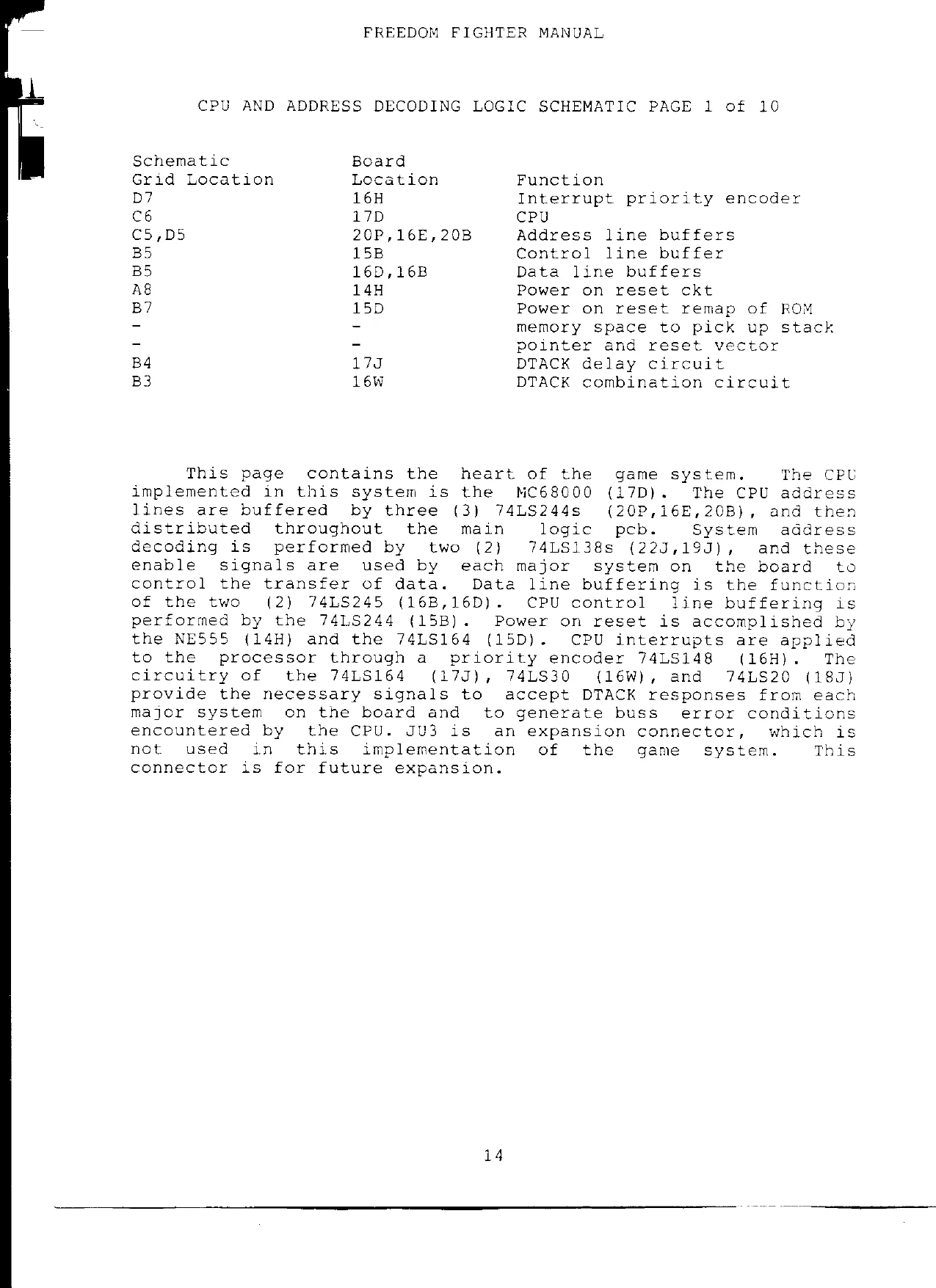
CPU AND ADDRESS DECODING LOGIC SCHEMATIC PAGE 1 of 10
| Grid Location | Location | Function |
| D? | 16H | Interrupt priority encoder |
| cé | 17D | CPU |
| c5,D5 | 20P,16E,20B | Address line buffers |
| BS | 15B | Control line buffer |
| B5 | 16D,16B | Data line buffers |
| Ag | 14H | Power on reset ckt |
| B7 | 15D | Power on reset remap of ROM |
| = | - | memory space to pick up stack |
| - | - | pointer and reset vector |
| B4 | 17d | DTACK delay circuit |
| B3 | 16W | DTACK combination circuit |
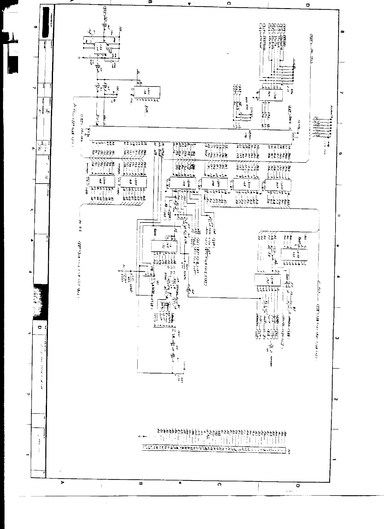
This page contains the heart of the game system. The CPU implemented in this system is the MC68000 (17D). The CPU address lines are buffered by three (3) 74LS244s (20P,16E,20B}), and then distributed throughout the main logic pcb. System address decoding is performed by two (2) 74LS138s (223,193), and these enable signals are used by each major system on the board to control the transfer of data. Data line buffering is the function of the two (2) 74L8245 (16B,16D). CPU control jline buffering is performed by the 7418244 (15B). Power on reset is accomplished by the NE555 (14H) and the 74LS164 (15D). CPU interrupts are applied to the processor through a priority encoder 74LS148 (16H). The circuitry of the 74LS164 (173), 74LS30 (16W), and 74LS20 (18d) provide the necessary signals to accept DTACK responses from each major system on the board and to generate buss error conditions encountered by the CPU. JU3 is an expansion connector, which is not used in this implementation of the game system. This connector is for future expansion.
This page is a drawing, shown as the original scan.
This page is a drawing, shown as the original scan.
This page is a drawing, shown as the original scan.
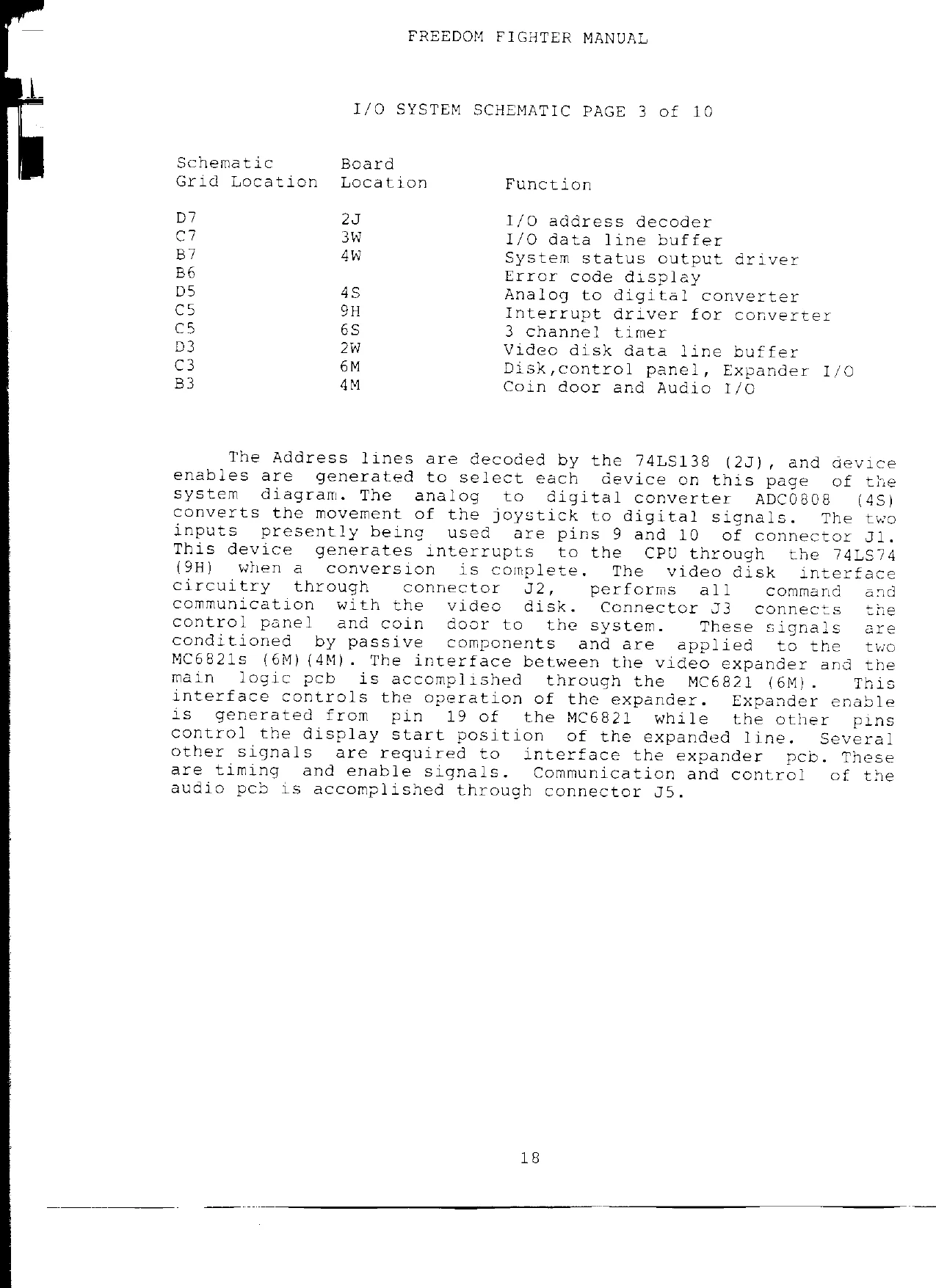
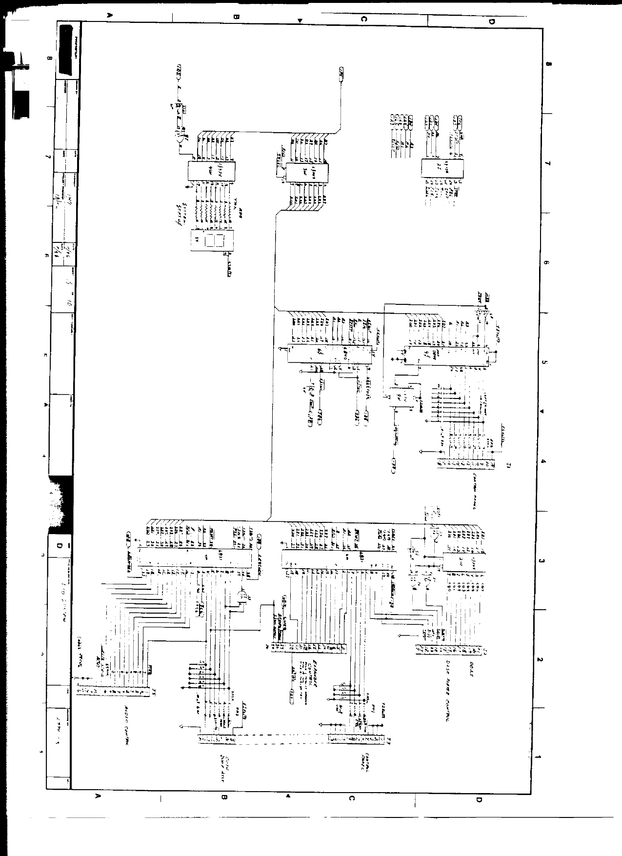
1/0 SYSTEM SCHEMATIC PAGE 3 of 10
Grid Location Location Function
| D7 | 2g | 1/0 address decoder |
| C7 | 3W | I/O data line buffer |
| B? | aw | System status output driver |
B6 Error code display
| DS | 4s | Analog to digital converter |
| €5 | SH | Interrupt driver for converter |
| cs | 6S | 3 channel timer |
| D3 | 20 | Video disk data line buffer |
| C3 | 6M | Disk,control panel, Expander 1/0 |
| B3 | 4M | Coin @oor and Audio 1/0 |
The Address lines are decoded by the 74LS138 (23), and device enables are generated to select each device on this page of the system diagram. The analog to digital converter aDC0808 (4S) converts the movement of the joystick to digital signals. The two inputs presently being used are pins 9 and 10 of connector Jl. This device generates interrupts to the CPU through the 74L$74 {9H} when a@ conversion is complete. The video disk interface circuitry through connector J2, performs all command and communication with the video disk. Connector J3 connects the control panel and coin door to the system. These signals are conditioned by passive components and are applied to the two MC682is (6M) (4M). The interface between the video expander and the main logic pcb is accomplished through the MC6821 (6M). This interface controls the operation of the expander. Expander enable is generated from pin 19 of the MC6821 while the other pins control the display start position of the expanded line. Several other signals are required to interface the expander pcb. These are timing and enable signals. Communication and control of the audio pcb is accomplished through connector J5.
This page is a drawing, shown as the original scan.
This page is a drawing, shown as the original scan.
This page is a drawing, shown as the original scan.
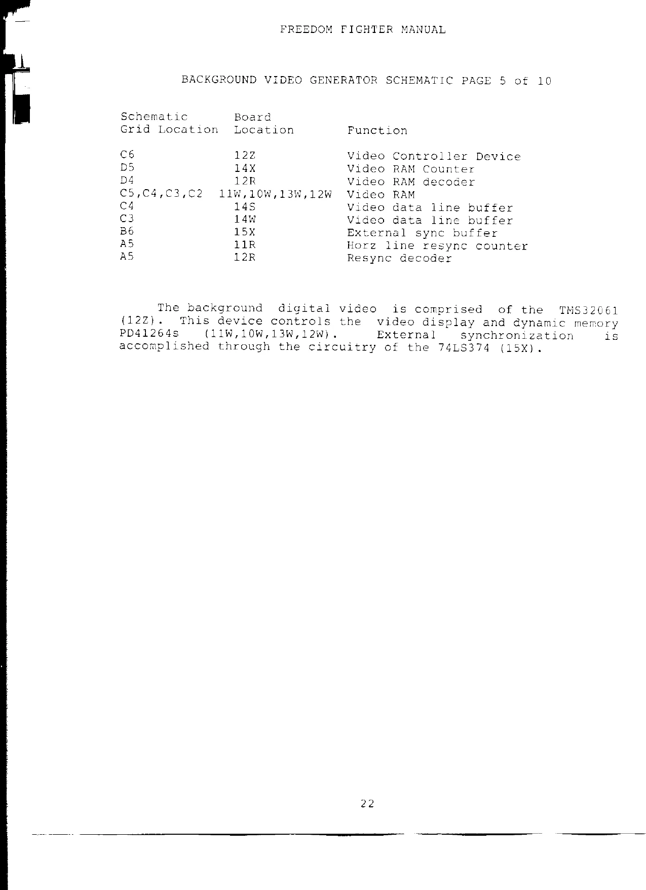
This page is a drawing, shown as the original scan.
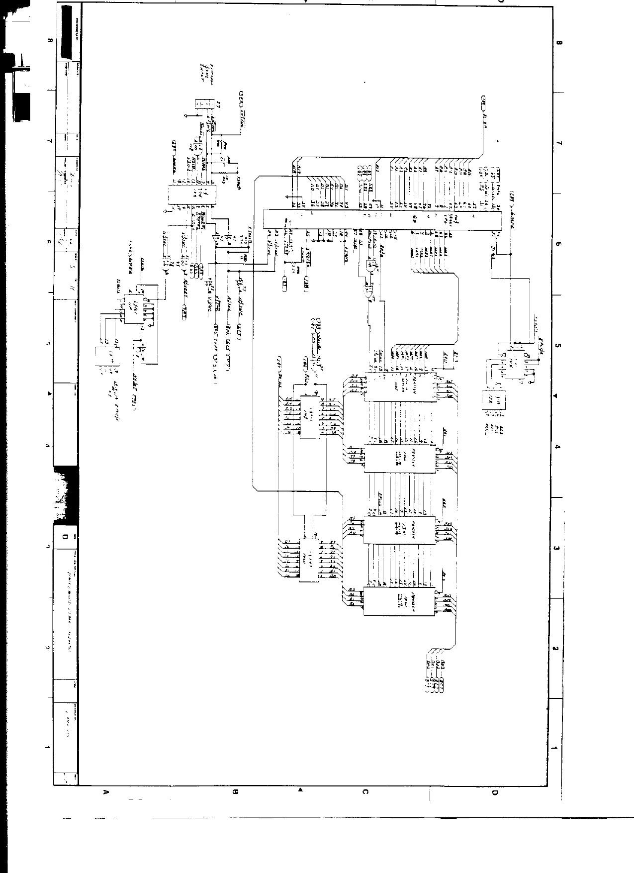
This page is a drawing, shown as the original scan.
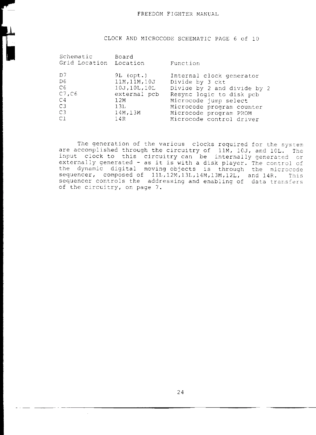
This page is a drawing, shown as the original scan.
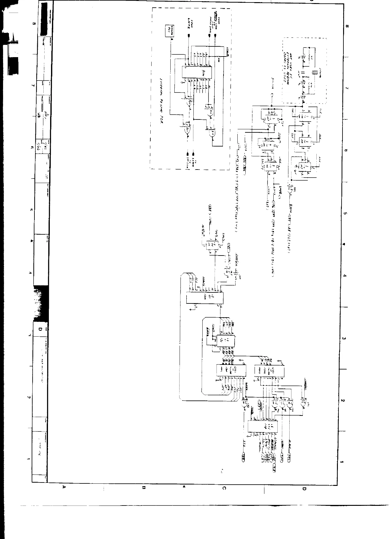
This page is a drawing, shown as the original scan.
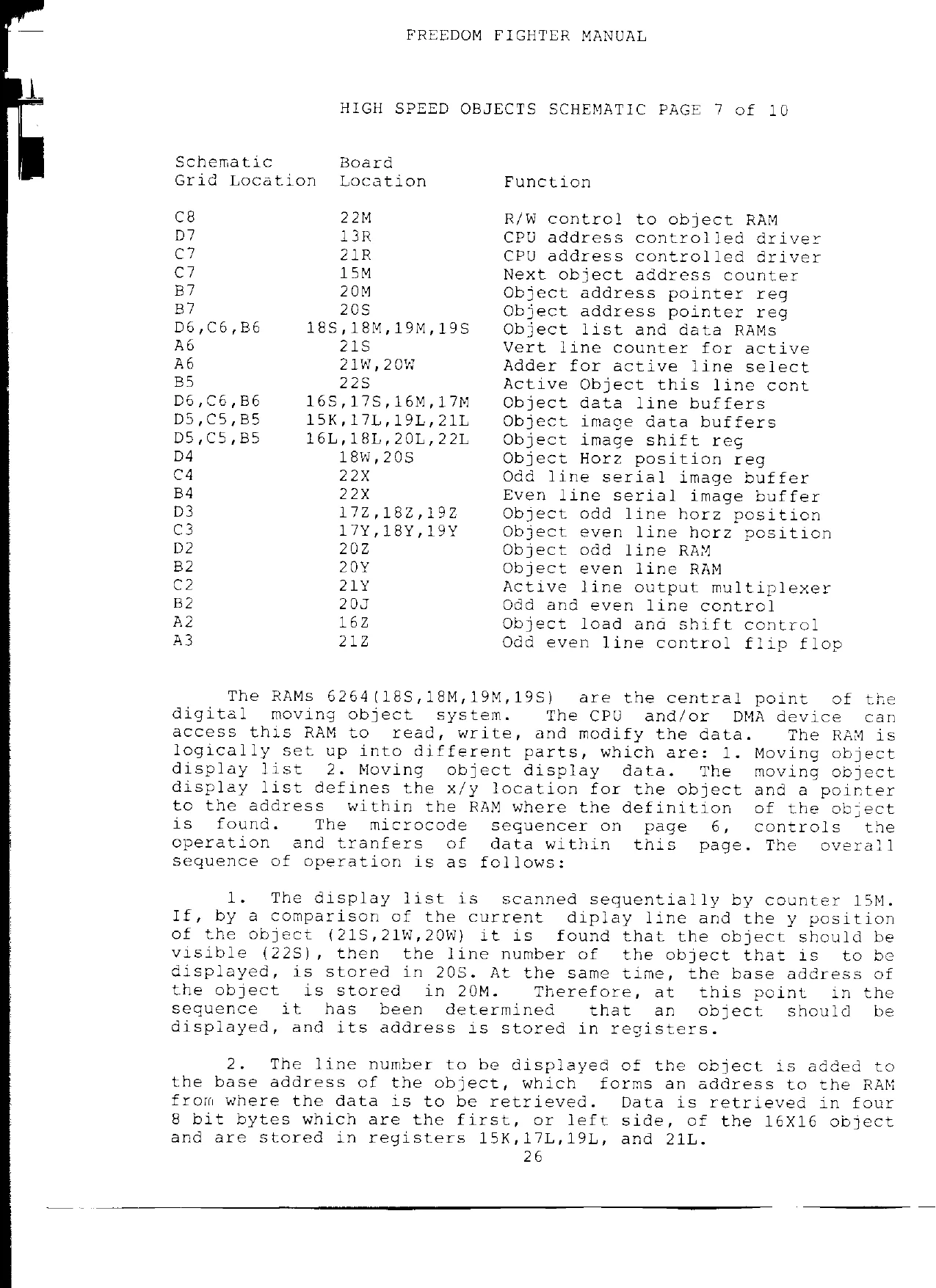
HIGH SPEED OBJECTS SCHEMATIC PAGE 7 of 10
Grid Location Location Function
| ce | 22M | R/W contre] to object RAM |
| D? | 13R | CPU address controlled driver |
| Cc? | 21R | CPU address controlled driver |
| Cc? | 15M | Next object address counter |
| B7 | 20M | Object address pointer reg |
| B7 | 20S | Object address pointer reg |
D6,C6,Bé 18S,18M,19M,19S Object list and data RAMs
| Ao | 21s | Vert line counter for active |
| Ab | 21W,20W | Adder for active line select |
| BS | 228 | Active Object this line cont |
D6,Cé, BE 16S,17S,16M,17M Object data line buffers D5,C5,B5 15K,17L,19L,21L Object image data buffers DS,C5,B5 16L,18L,20L,22L Object image shift reg
| D4 | 18W,205 | Object Horz position reg |
| c4 | 22X | Odd line serial image buffer |
| B4 | 22x | Even line serial image buffer |
| D3 | 172,182,192 | Object odd line horz position |
| c3 | 17¥,18Y,19Y | Object even line horz position |
| b2 | 202 | Object odd line RAM |
| B2 | 20¥ | Object even line RAM |
| C2 | 21y | Active line output multiplexer |
| B2 | 207 | Odd and even line contrel |
| AZ | 162 | Object load ana shift control |
| A3 | 212 | Odd even line control flip flop |
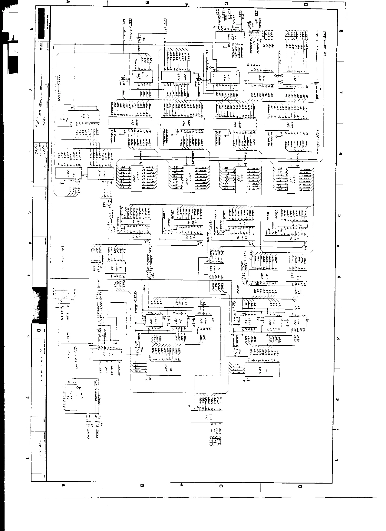
The RAMs 6264(18S,18M,19M,19S) are the central point of the digital moving object system. The CPU and/or DMA device can access this RAM to read, write, and modify the data. The RAM is logically set up into different parts, which are: 1. Moving object display list 2. Moving object display data. The moving object @isplay list defines the x/y location for the object and a pointer to the address within the RAM where the definition of the object is found. The microcode seguencer on page 6, controls the operation and tranfers of data within this page. The overall sequence of operation is as follows:
- The display list is scanned sequentially by counter 15M. If, by a comparison of the current diplay line and the y position of the object (218,21W,20W) it is found that the object should be visible (22S), then the line number of the object that is to be displayed, is stored in 205. At the same time, the base address of the object is stored in 20M. Therefore, at this point in the sequence it has been determined that an object should be displayed, and its address is stored in registers.
- The line number to be displayed of the object is added to the base address of the object, which forms an address to the RAM from where the data is to be retrieved. Data is retrieved in four 8 bit bytes which are the first, or left side, of the 16X16 object and are stored in registers 15K,17L,19L, and 21L.
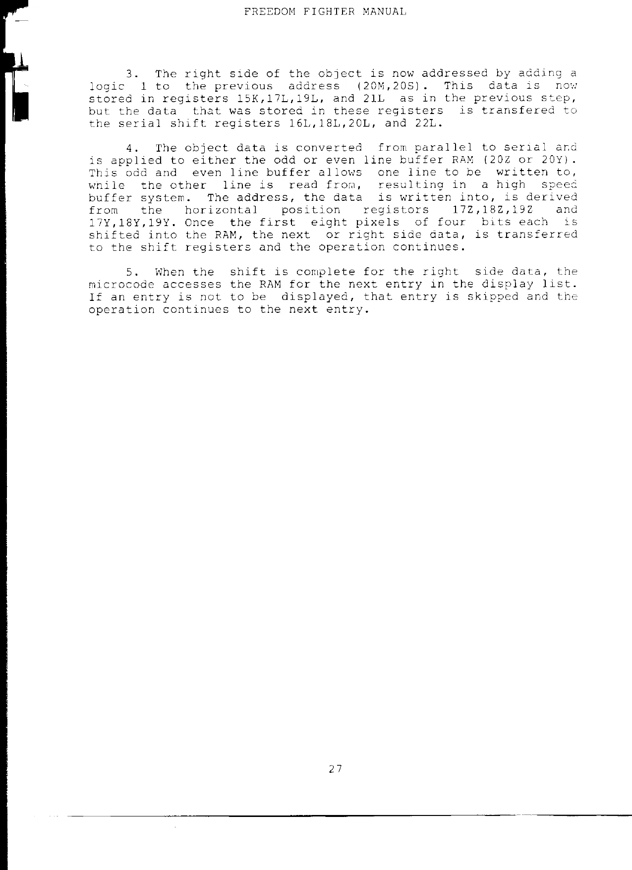
- The right side of the object is now addressed by adding a logic 1 to the previous address (20M,20S). This data is now stored in registers 15K,17L,19L, and 21L as in the previous step, but the data that was stored in these registers is transfered to the serial shift registers 16L,18L,20L, and 22L.
- The cbject data is converted from parallel to serial and is applied to either the odd or even line buffer RAM (202 or 20Y¥). This odd and even line buffer allows one line to be written to, wnile the cther line is read from, resulting in a high speed buffer system. The address, the data is written into, is derived from the horizontal position registors 172,182,192 and 17¥,18Y,19Y. Once the first eight pixels of four bits each is shifted into the RAM, the next or right side data, is transferred to the shift registers and the operation continues.
- When the shift is complete for the right side data, the microcode accesses the RAM for the next entry in the display list. If an entry is not to be displayed, that entry is skipped and the operation continues to the next entry.
This page is a drawing, shown as the original scan.
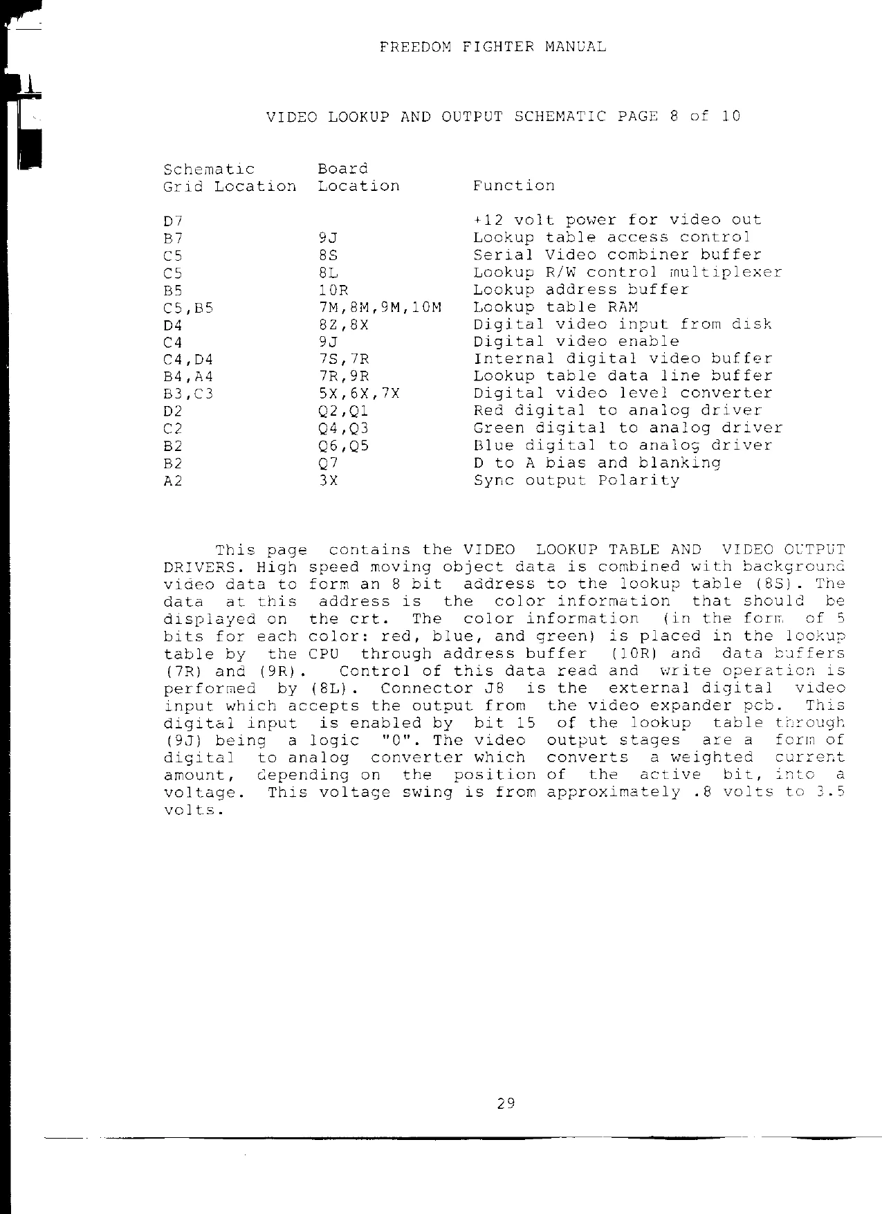
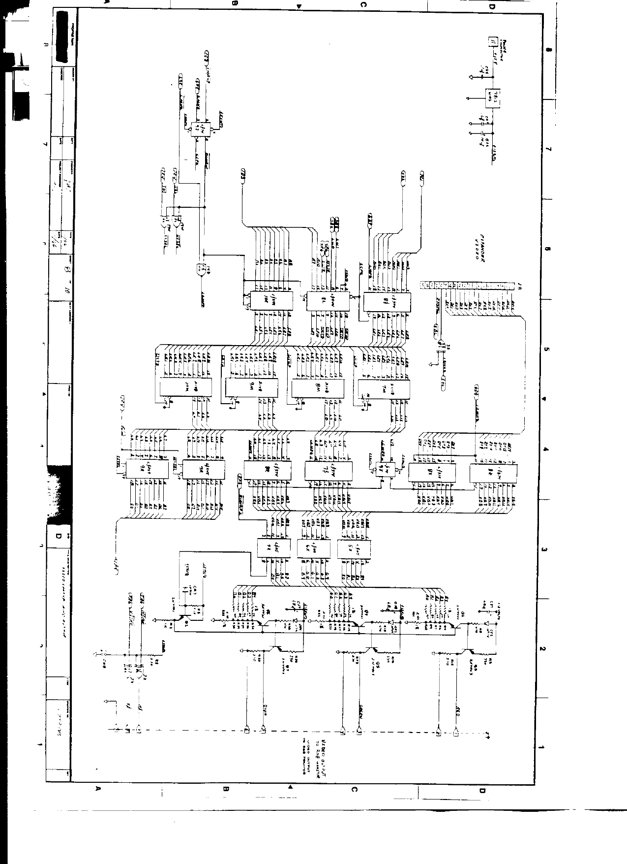
VIDEO LOOKUP AND OUTPUT SCHEMATIC PAGE 8 of 10
Grid Location Location Function
D7? +12 volt power for video out
| B? | gd | Lookup table access control |
| cs | 8S | Serial Video combiner buffer |
| cs | 8L | Lookup R/W control multiplexer |
| B5 | 10R | Lookup address buffer |
C5,B5 7M,8M,9M,10M Lookup table RAM
| D4 | 82 ,8X | Digital video input from disk |
| c4 | oo | Digital video enable |
| c4,D4 | 785,7R | Internal digital video buffer |
| B4,A4 | 7R,9R | Lookup table data line buffer |
| B3,C3 | 5X,6X,7xX | Digital video level converter |
| D2 | 02,01 | Red digital to analog driver |
| c2 | Q4,03 | Green digital to analog driver |
| B2 | 06,05 | Blue digital to analog driver |
| B2 | Q7 | D to A bias and blanking |
| AZ | 3X | Syne output Polarity |
This page contains the VIDEO LOOKUP TABLE AND VIDEO OUTPUT DRIVERS. High speed moving object data is combined with background video data to form an 8 bit address to the lookup table (85). The data at this address is the color information that should be displayed on the crt. The color information (in the form of 5 bits for each color: red, blue, and green) is placed in the lookup table by the CPU through address buffer (JOR) and data buffers (7R) and (9R). Control of this data read and write operation is performed by (8L}. Connector J8 is the external digital video input which accepts the output from the video expander pcb. This digital input is enabled by bit 15 of the lookup table through
- being a logic "0". The video output stages are a form of digital to analog converter which converts a weighted current amount, depending on the position of the active bit, into a4 voltage. This voltage swing is from approximately .8 volts to 2.5 volts.
This page is a drawing, shown as the original scan.
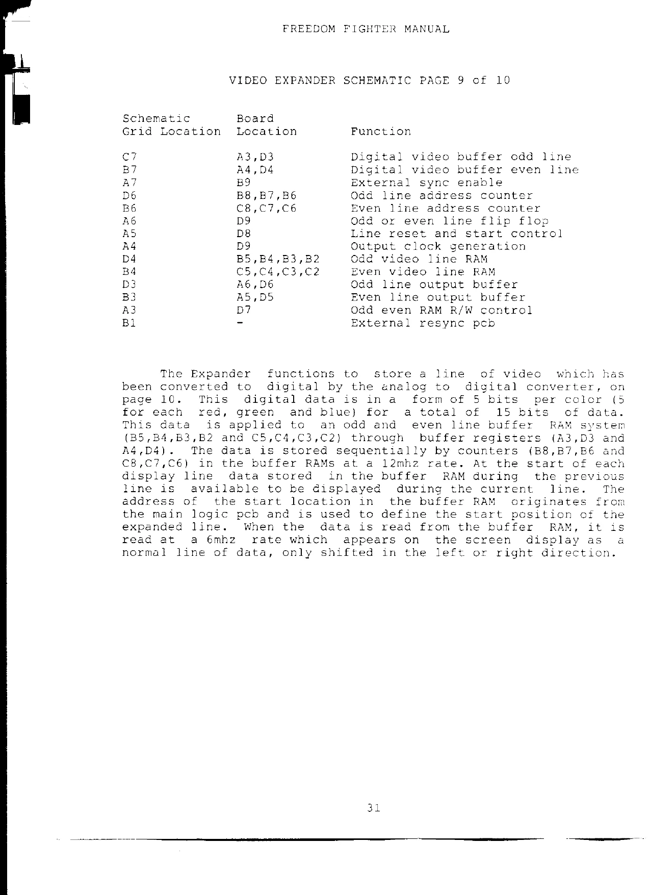
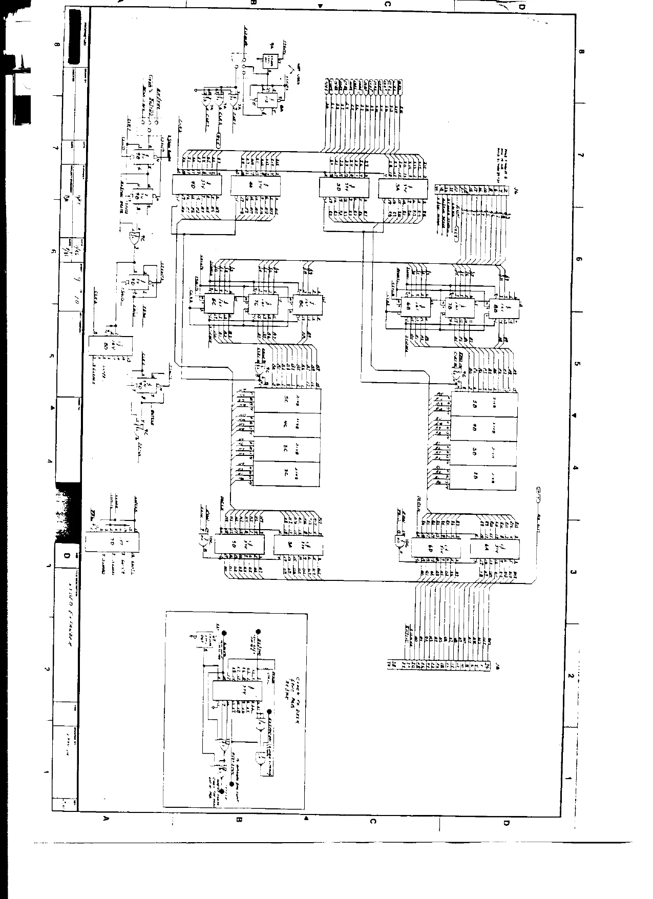
VIDEO EXPANDER SCHEMATIC PAGE 9 of 10
Grid Location Location Function
| CF | A3,D3 | Digital video buffer odd line |
| B? | A4,D4 | Digital video buffer even line |
| Al | Bo | External sync enable |
| D6 | B8,B7,56 | Odd line address counter |
| B6 | c8,C7,C6 | Even line address counter |
| AG | DS | Odd or even line flip flop |
| AS | DB | Line reset and start control |
| A4 | Dg | Output clock generation |
| D4 | BS,B4,53,B2 | Oda video line RAM |
| B4 | c5,C4,C3,C2 | Even video line RAM |
| D3 | A6,D6 | Odd line output buffer |
| B3 | A5,D5 | Even line output buffer |
| A3 | D7 | Odd even RAM R/W control |
| Bl | - | External resync peb |
The Expander functions to store a line of video which has been converted to digital by the enalog to digital converter, on page 10. This digital data is in a form of 5 bits per color (5 for each red, green and biue) for a total of 15 bits of data. This data is applied to an odd and even line buffer RAM system (B5,B4,B3,B2 and C5,C4,C3,C2}) through buffer registers (A3,D3 and A4,D4). The data is stored sequentially by counters (B8,B7,B6 and c8,C7,C6) in the buffer RAMs at a 12mhz rate. At the start of each display line data stored in the buffer RAM during the previous line is available to be displayed during the current line. The address of the start location in the buffer RAM originates from the main logic pcb and is used to define the start position of the expanded line. When the data is read from the buffer RAM, it is read at a 6mhz rate which appears on the screen display as a4 normal line of data, only shifted in the left or right direction.
This page is a drawing, shown as the original scan.
This page is a drawing, shown as the original scan.
This page is a drawing, shown as the original scan.
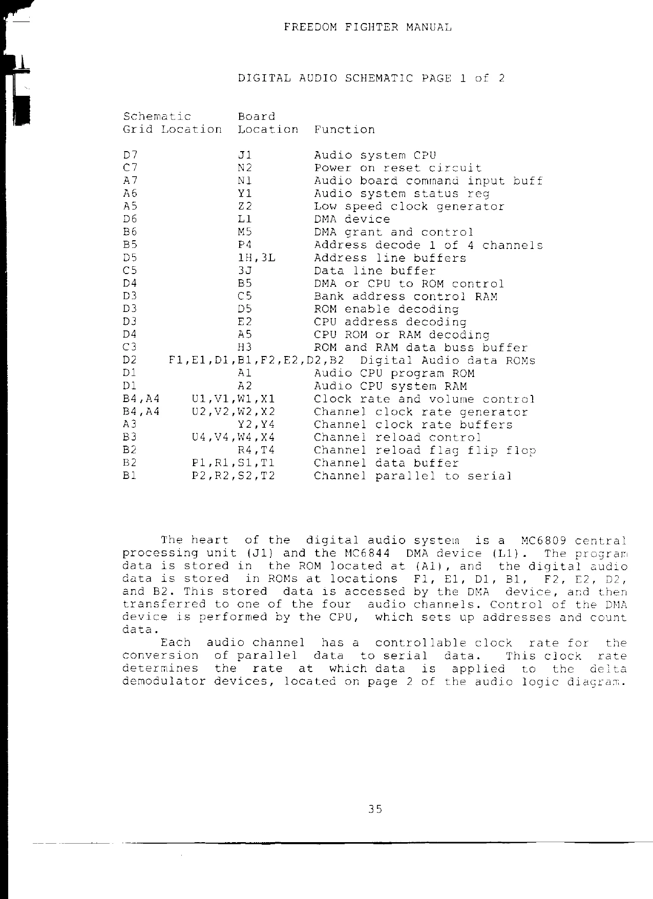
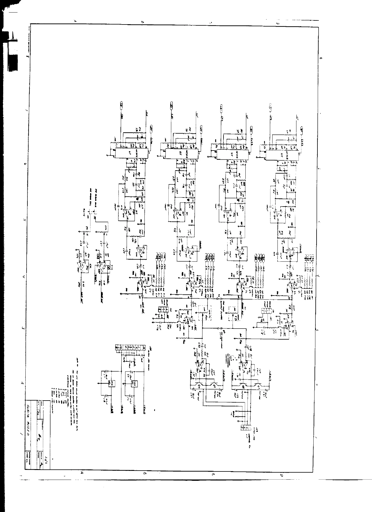
DIGITAL AUDIO SCHEMATIC PAGE 1 of 2
Grid Location Location Function
| D7? | o1 | Audio system CPU |
| C7 | N2 | Power on reset circuit |
| A? | Ni | Audio board command input buff |
| AG | Yi | Audio system status reg |
| AS | 22 | Low speed clock generator |
| D6 | LL | DMA device |
| B6 | MS | DMA grant and control |
| B5 | P4 | Address decode 1 of 4 channels |
| D5 | 1H,3L | Address line buffers |
| cs | 3d | Data line buffer |
| D4 | BS | DMA or CPU to ROM control |
| D3 | es | Bank address control RAM |
| D3 | DS | ROM enable decoding |
| D3 | E2 | CPU address decoding |
| D4 | AS | CPU ROM or RAM decoding |
| C3 | H3 | ROM and RAM data buss buffer |
D2 F1,E1,D1,B1,F2,E2,D2,82 Digital Audio data ROMs
| Di | Al | Audio CPU program ROM |
| Di | A2 | Audio CPU system RAM |
| B4,A4 | U1,V1,W1,X1 | Clock rate and volume control |
| B4,A4 | U2,V2,W2,X2 | Channel] clock rate generator |
| Ai | Y2,Y4 | Channel clock rate buffers |
| B3 | U4,V4,W4,X4 | Channel reload control |
| B2 | R4,T4 | Channel reload flag flip flop |
| B2 | P1,R1,S1,T1 | Channel data buffer |
| Bl | P2,R2,S2,T2 | Channel parallel to serial |
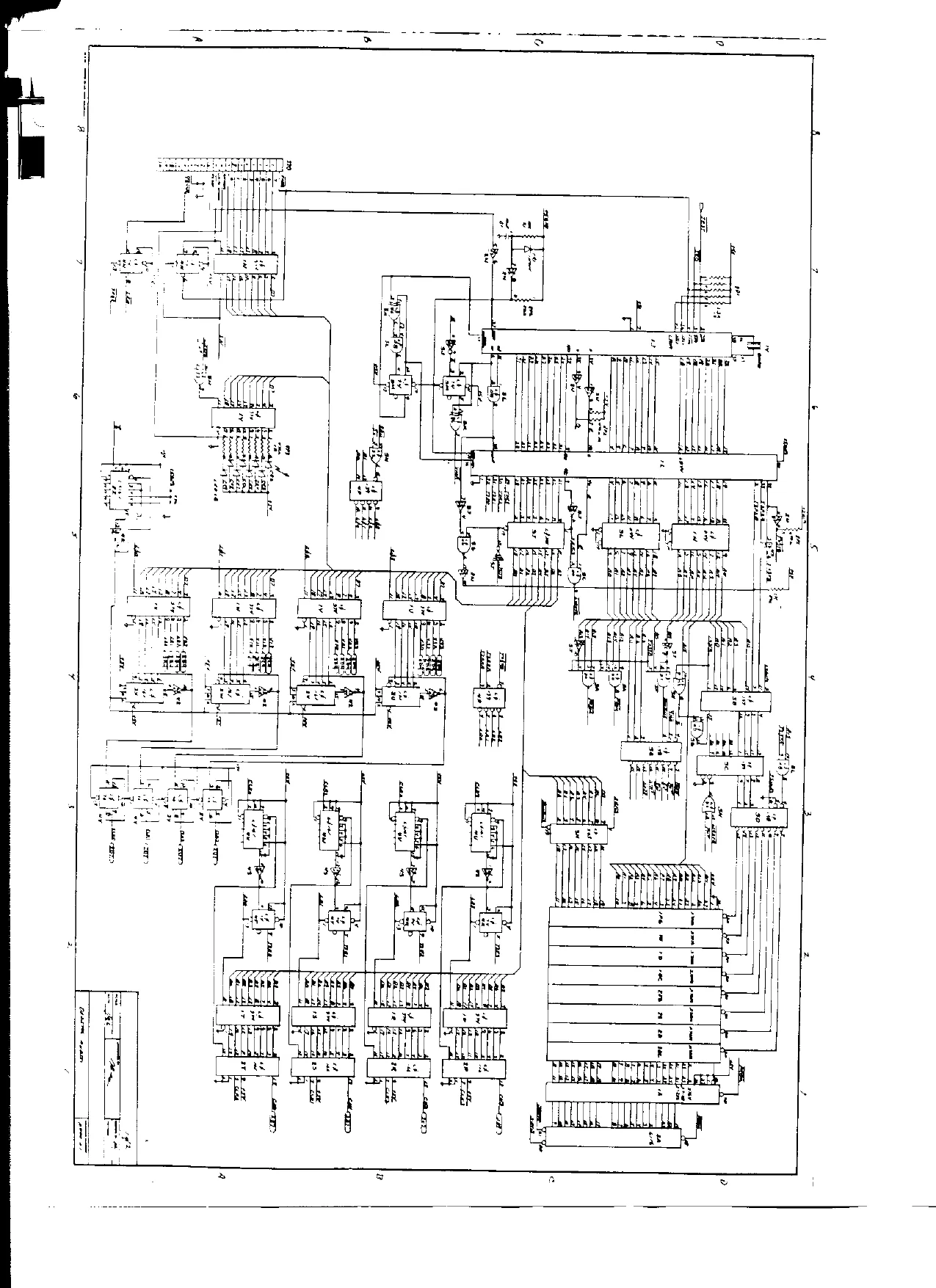
The heart of the digital audio system is a MC6809 central processing unit (J1) and the MC6844 DMA device (Ll). The program data is stored in the ROM located at (Ai), and the digital audio Gata is stored in ROMs at locations Fi, El, Dl, Bl, F2, E2, D2, and BZ. This stored data is accessed by the DMA device, and then transferred to one of the four audio channels. Control of the DMA device is performed by the CPU, which sets up addresses and count data. Each audio channel has a controllable clock rate for the conversion of parallel data to serial data. This clock rate determines the rate at which data is applied to the deita demodulator devices, located on page 2 of the audio logic diagram.
This page is a drawing, shown as the original scan.
This page is a drawing, shown as the original scan.
This page is a drawing, shown as the original scan.
This page is a drawing, shown as the original scan.