Food Fight SP-229 1st Printing
Food Fight (rev 3) (General Computer Corporation (Atari license), 1982) · Schematic Package · 22 pages · 31 sections · original scan
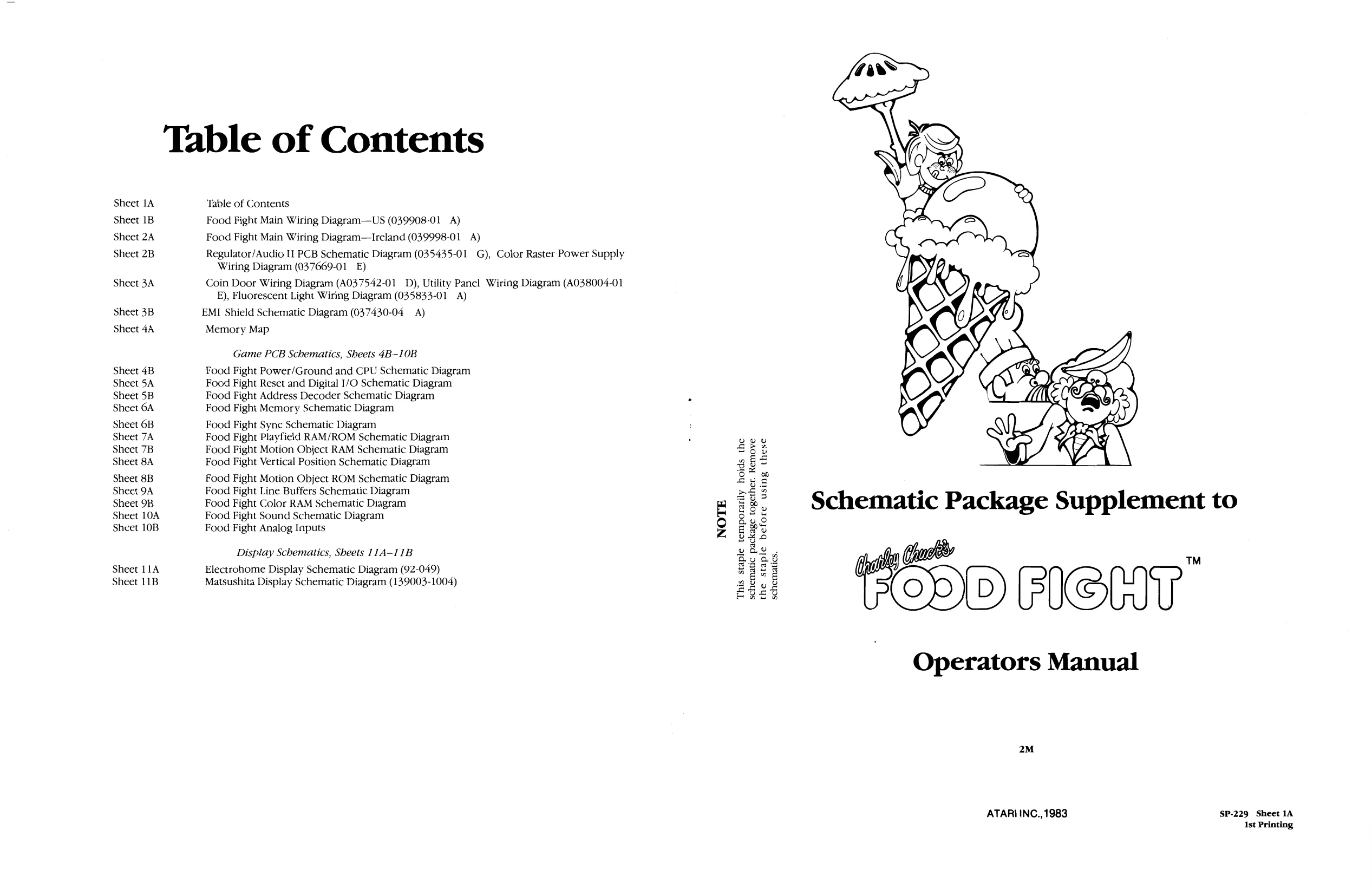
Table of Contents
Sheet 1A Table of Contents Sheet 1B Food Fight Main Wiring Diagram—US (039908-01 A) Sheet 2A Food Fight Main Wiring Diagram—Ireland (039998-01 A) Sheet 2B Regulator/Audio I] PCB Schematic Diagram (035435-01 G), Color Raster Power Supply Wiring Diagram (037669-01 E) Sheet 3A Coin Door Wiring Diagram (A037542-01 D), Utility Panel Wiring Diagram (A038004-01 E), Fluorescent Light Wiring Diagram (035833-01 A) Sheet 3B EMI Shield Schematic Diagram (037430-04 A) Sheet 4A Memory Map
Game PCB Schematics, Sheets 4B-10B Sheet 4B Food Fight Power/Ground and CPU Schematic Diagram Sheet 5A Food Fight Reset and Digital I/O Schematic Diagram Sheet 5B Food Fight Address Decoder Schematic Diagram . Sheet 6A Food Fight Memory Schematic Diagram Sheet 6B Food Fight Syne Schematic Diagram Sheet 7A Food Fight Playfield RAM/ROM Schematic Diagram. eve Sheet 7B Food Fight Motion Object RAM Schematic Diagram 266 Sheet 8A Food Fight Vertical Position Schematic Diagram 3 5 bo} Sheet 8B Food Fight Motion Object ROM Schematic Diagram 2 3 2 Sheet 9A Food Fight Line Buffers Schematic Diagram Bes e sheet 9B Food Fight Color RAM Schematic Diagram # 22, Schematic Package Supplement to Sheet 10A Food Fight Sound Schematic Diagram B 8 vo Sheet 10B Food Fight Analog Inputs 9 2S Zz p28 Display Schematics, Sheets 11A-11B ghey Cua ™ Sheet 11A Electrohome Display Schematic Diagram (92-049) 5] 3 § = Sheet 11B Matsushita Display Schematic Diagram (139003-1004) 2202 G Begsy
Operators Manual
2M
ATARI INC.,1983 SP-229 Sheet 1A Ist Printing
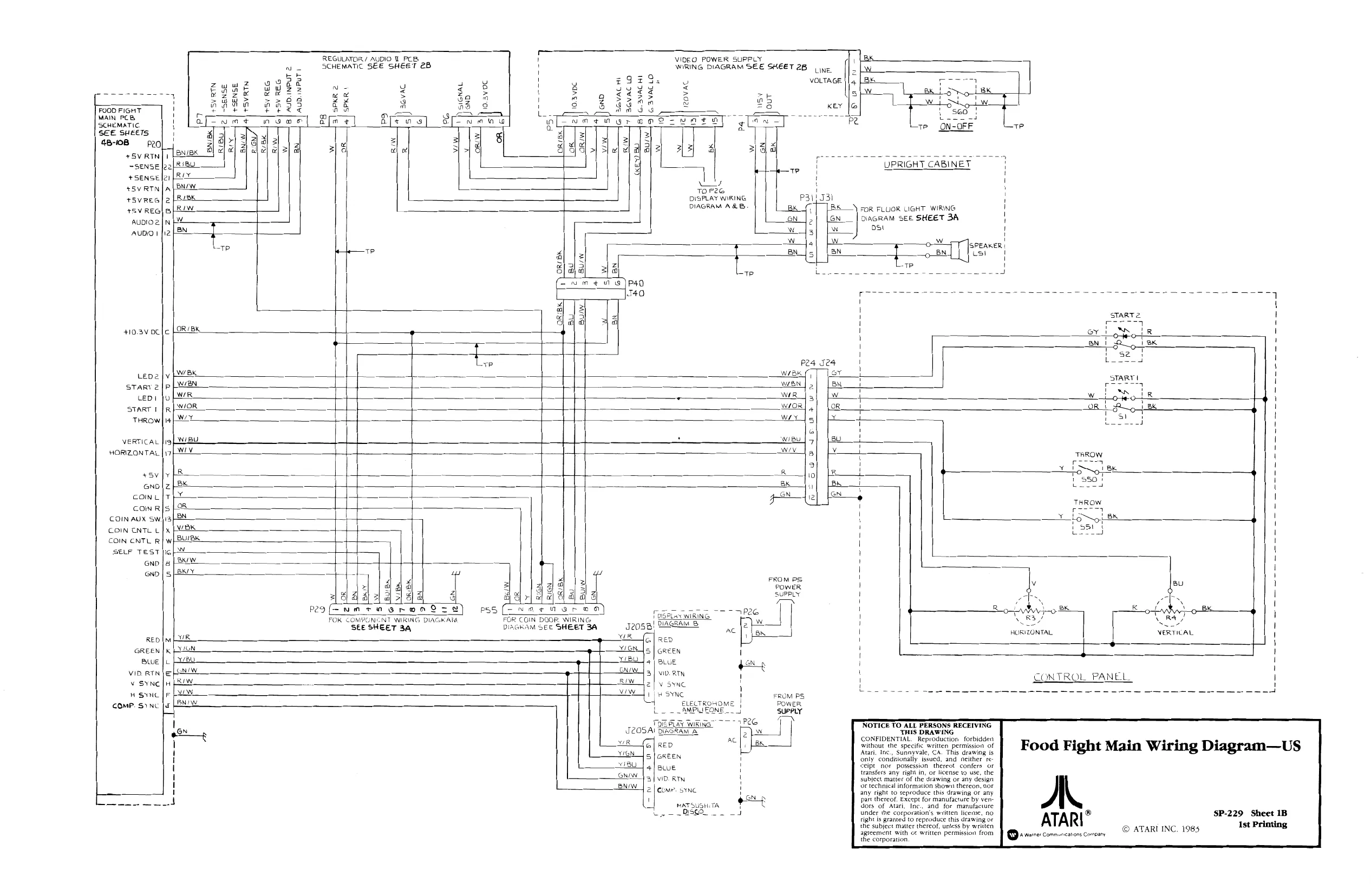
This page is a drawing, shown as the original scan.
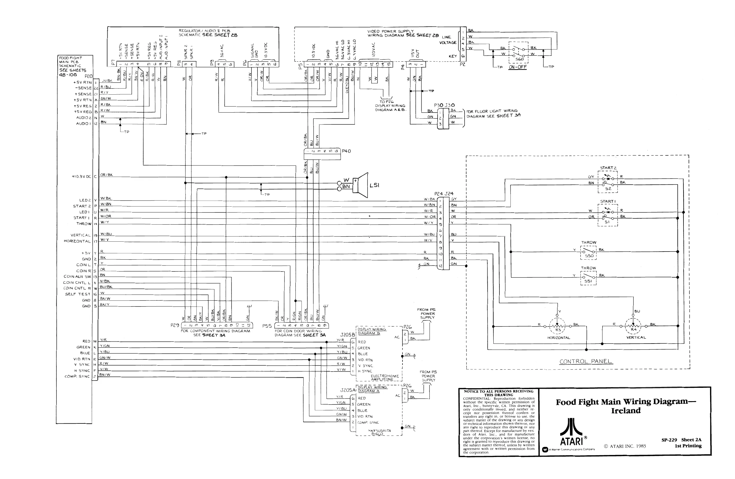
This page is a drawing, shown as the original scan.
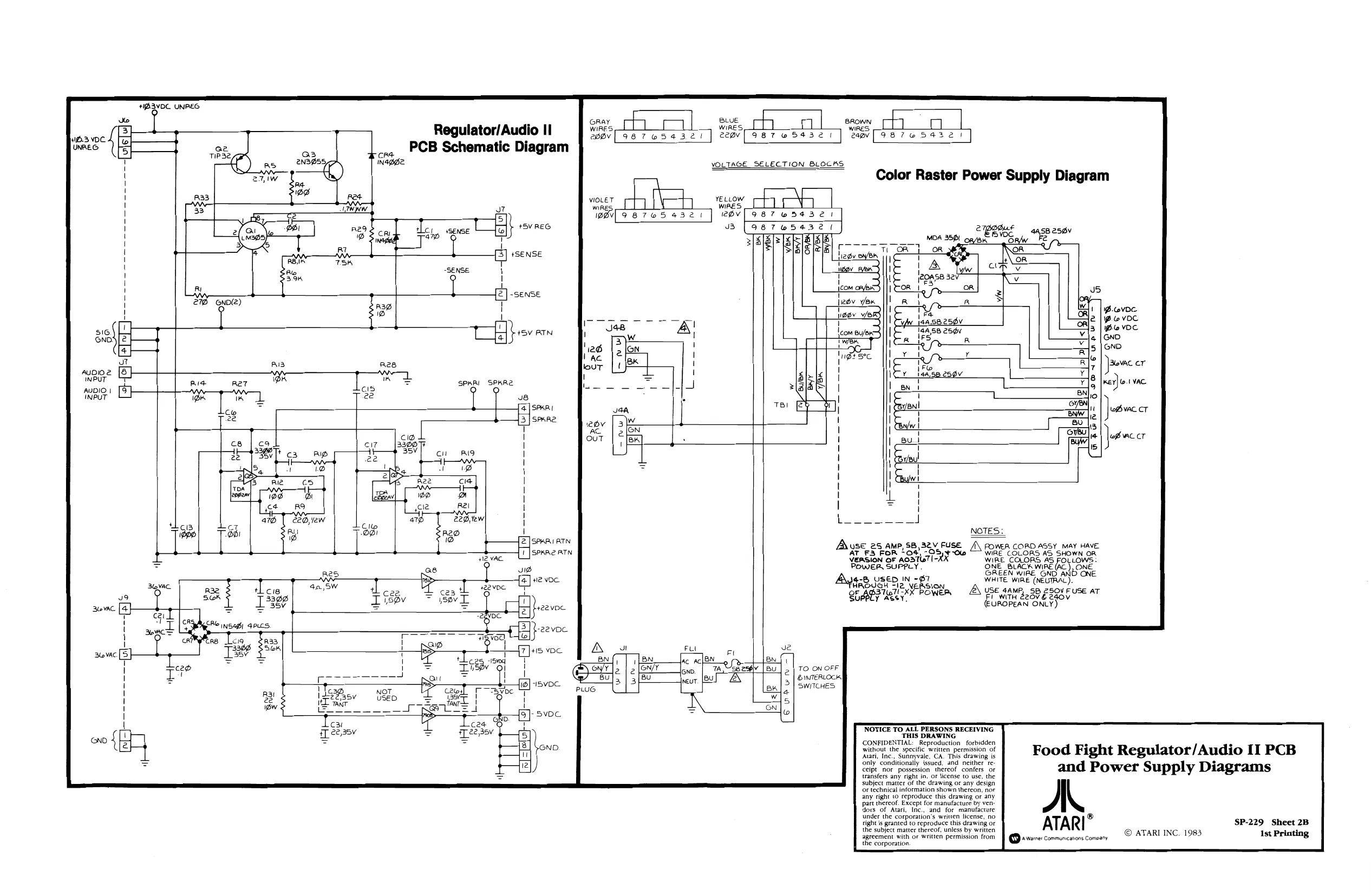
This page is a drawing, shown as the original scan.
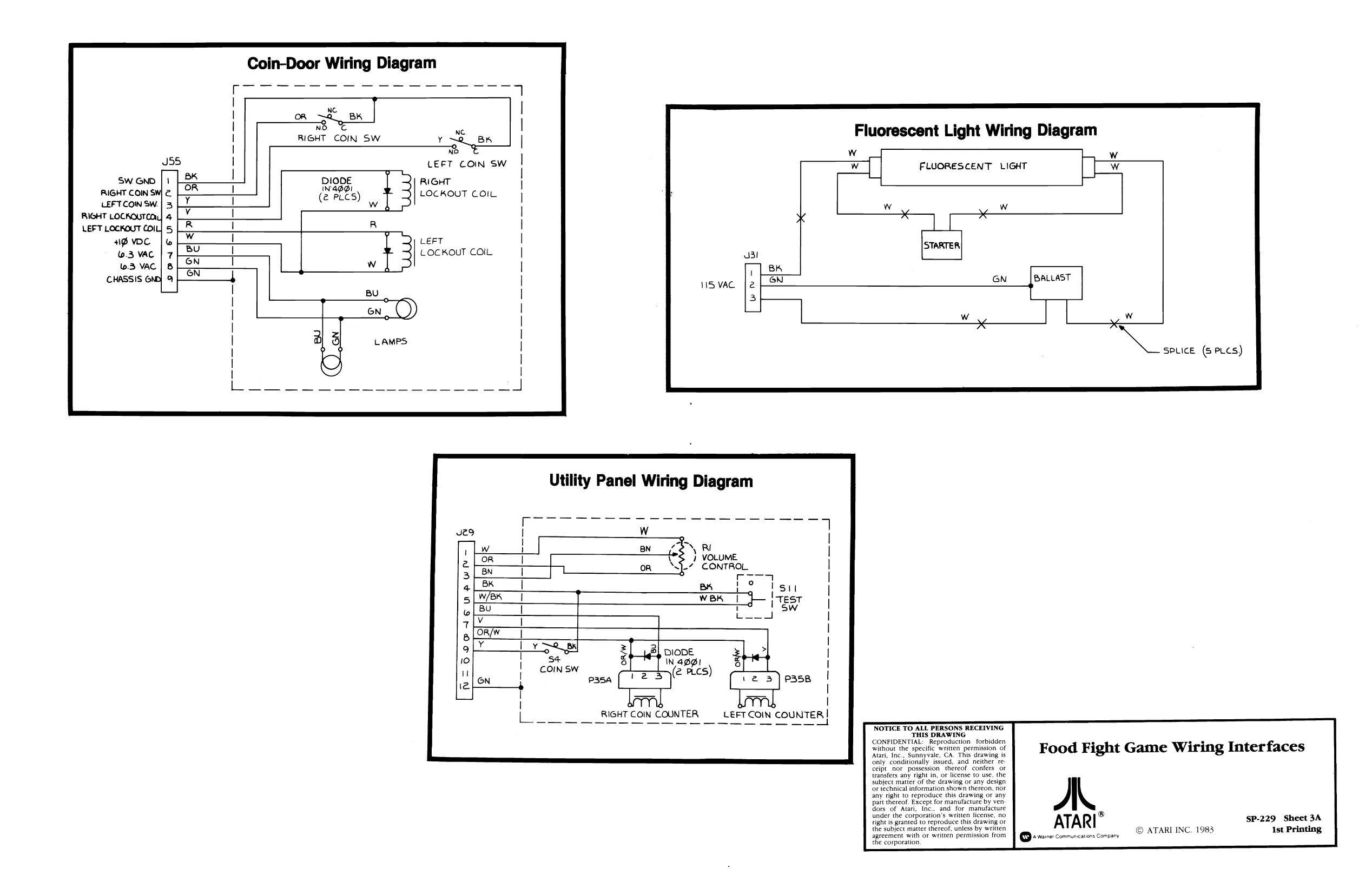
This page is a drawing, shown as the original scan.
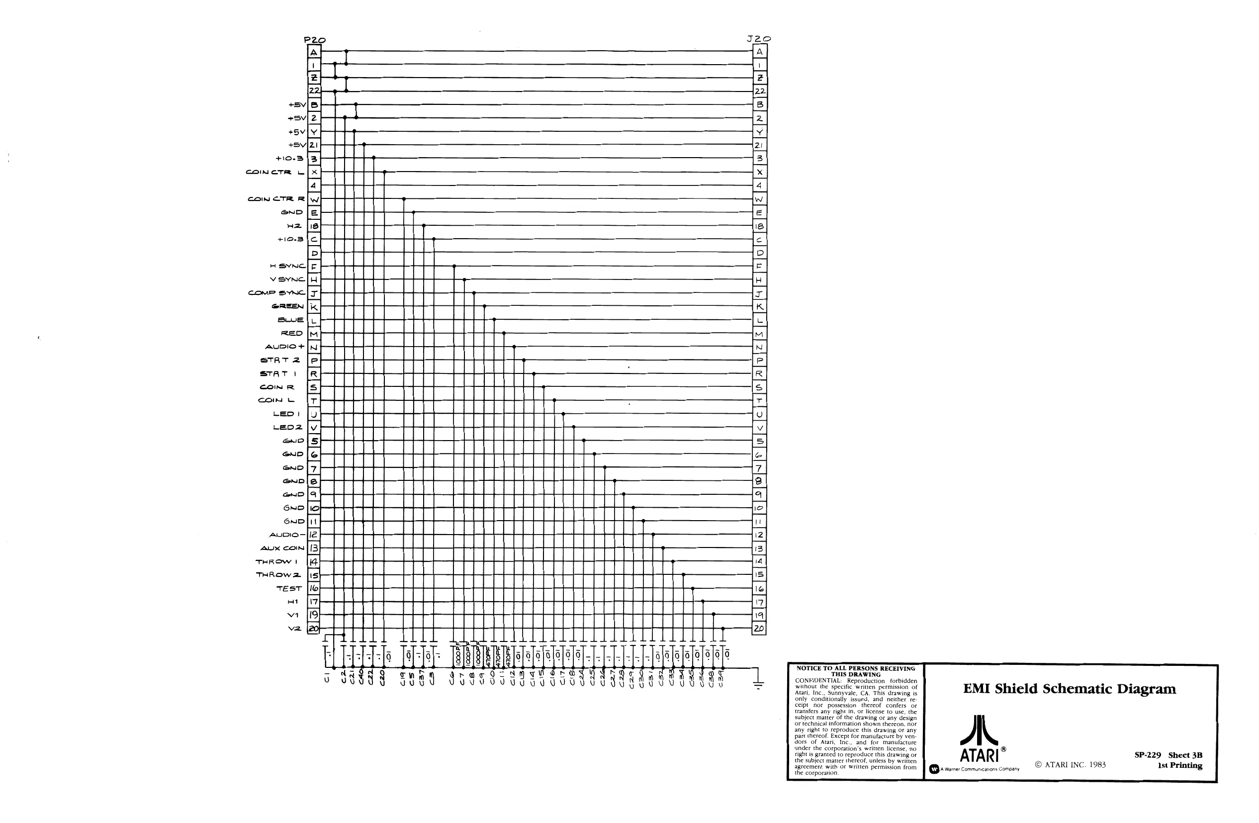
This page is a drawing, shown as the original scan.
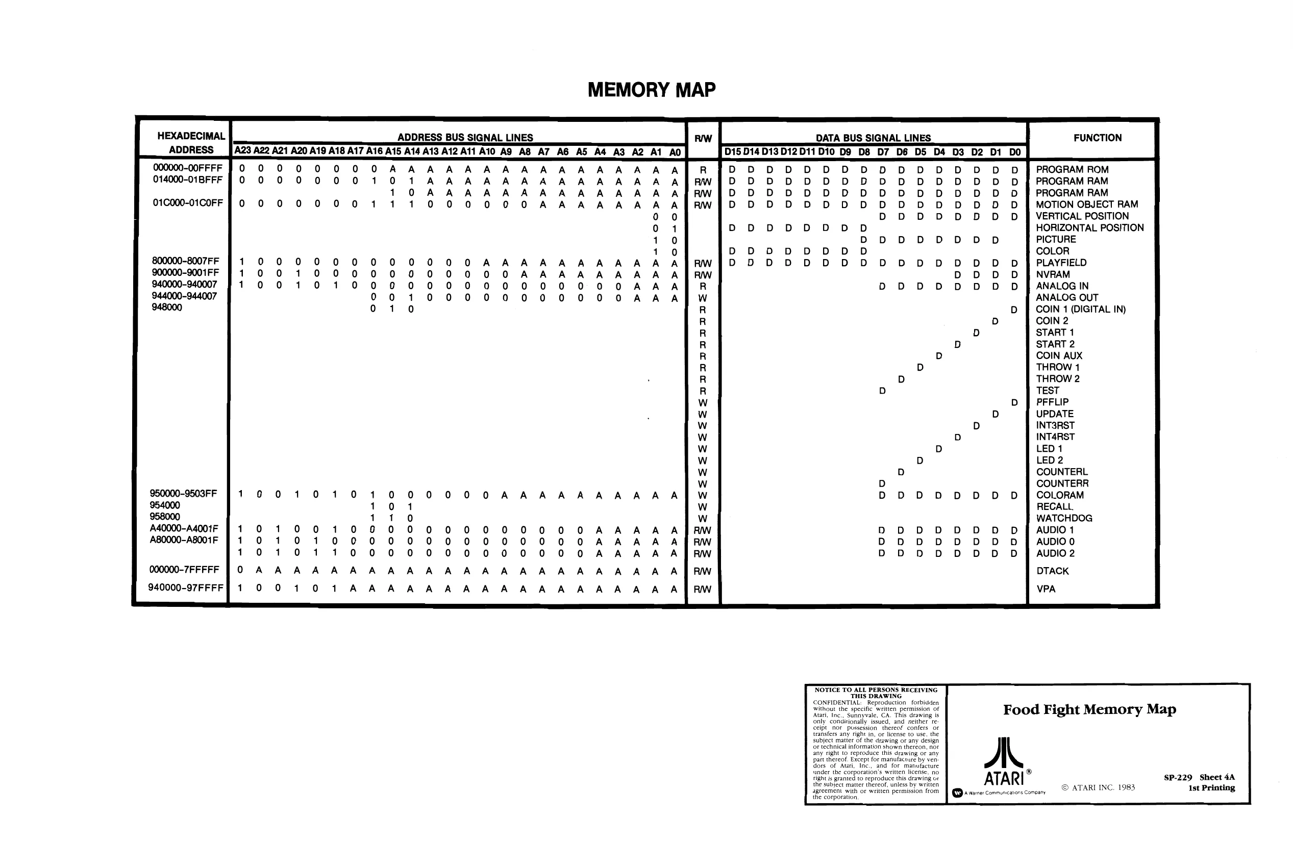
This page is a drawing, shown as the original scan.
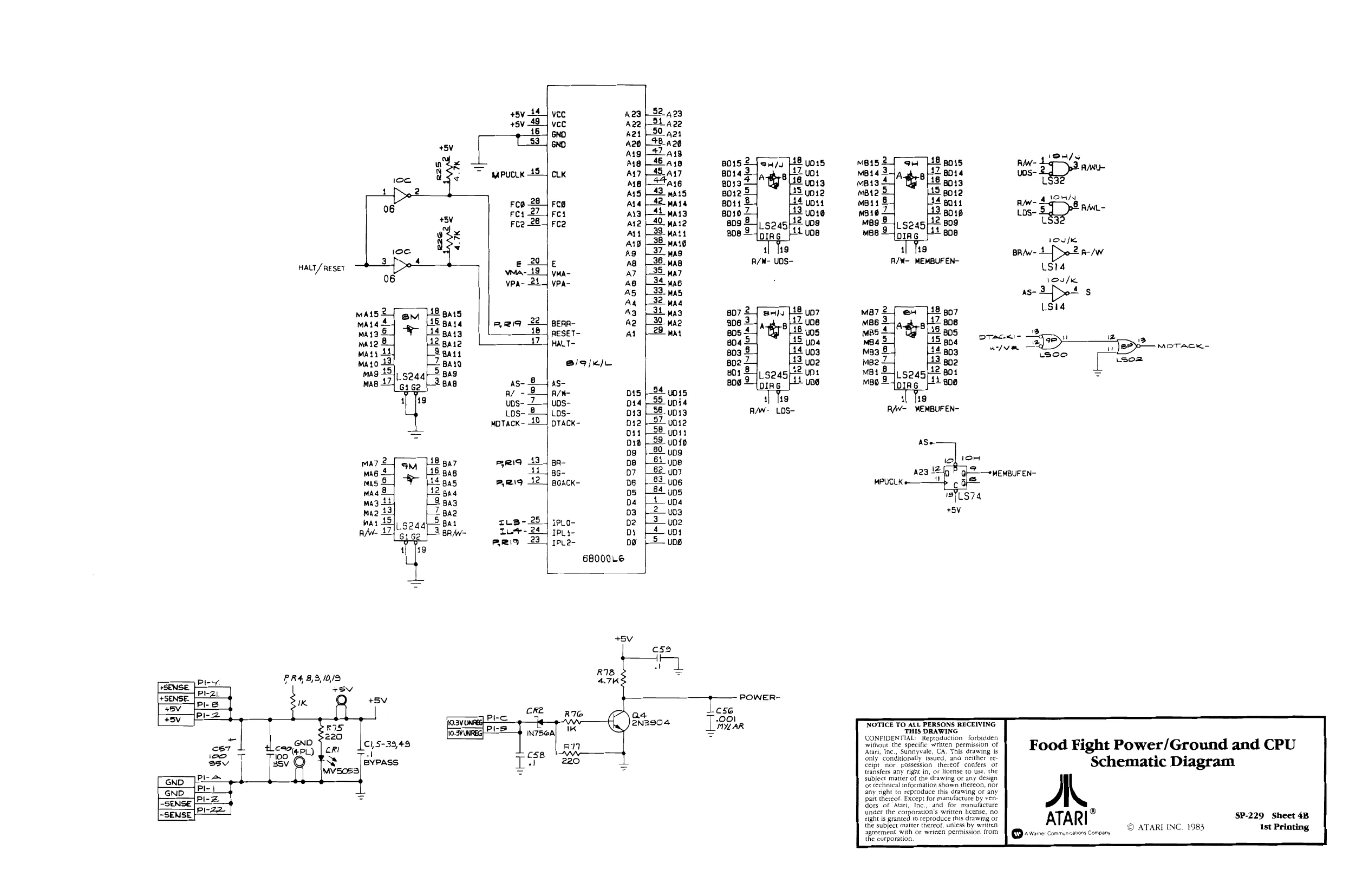
This page is a drawing, shown as the original scan.
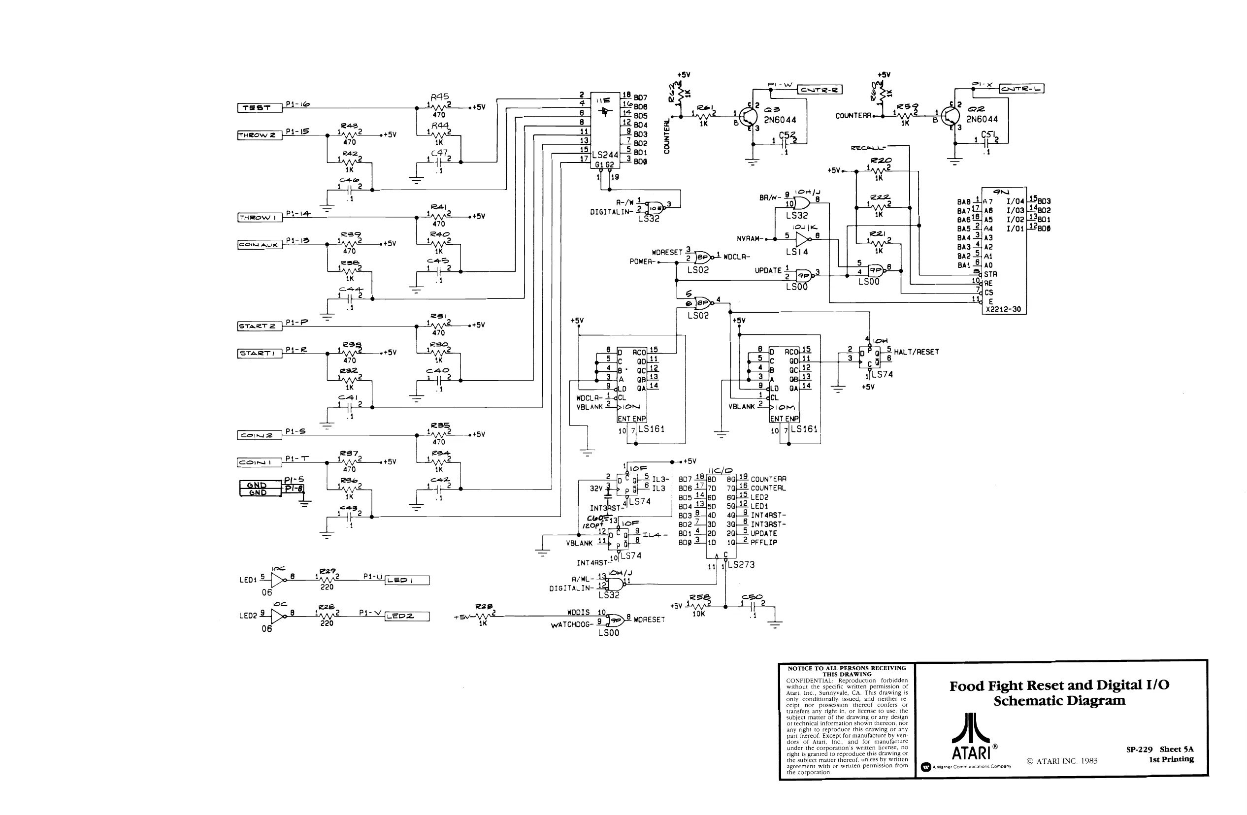
This page is a drawing, shown as the original scan.
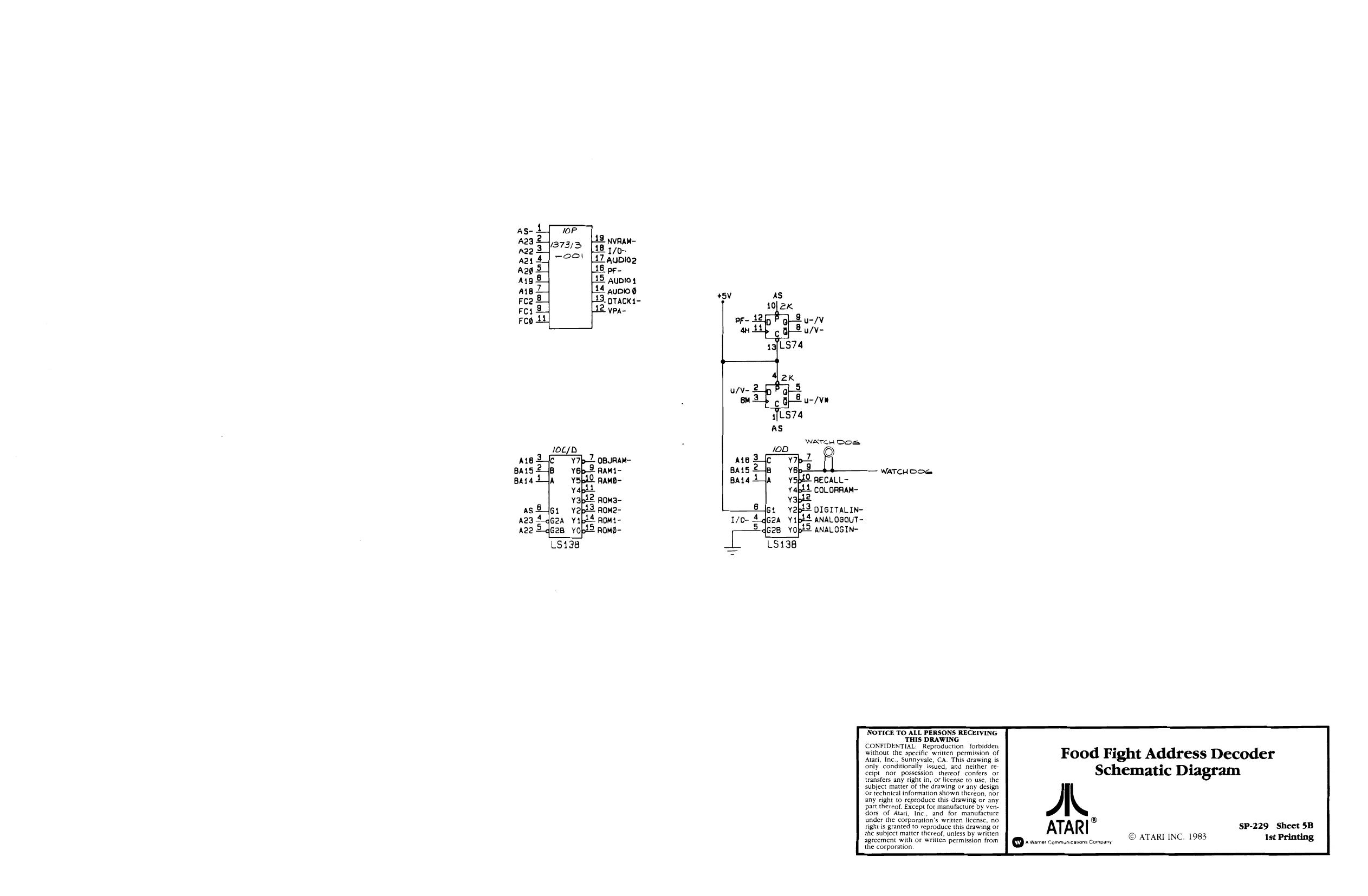
This page is a drawing, shown as the original scan.
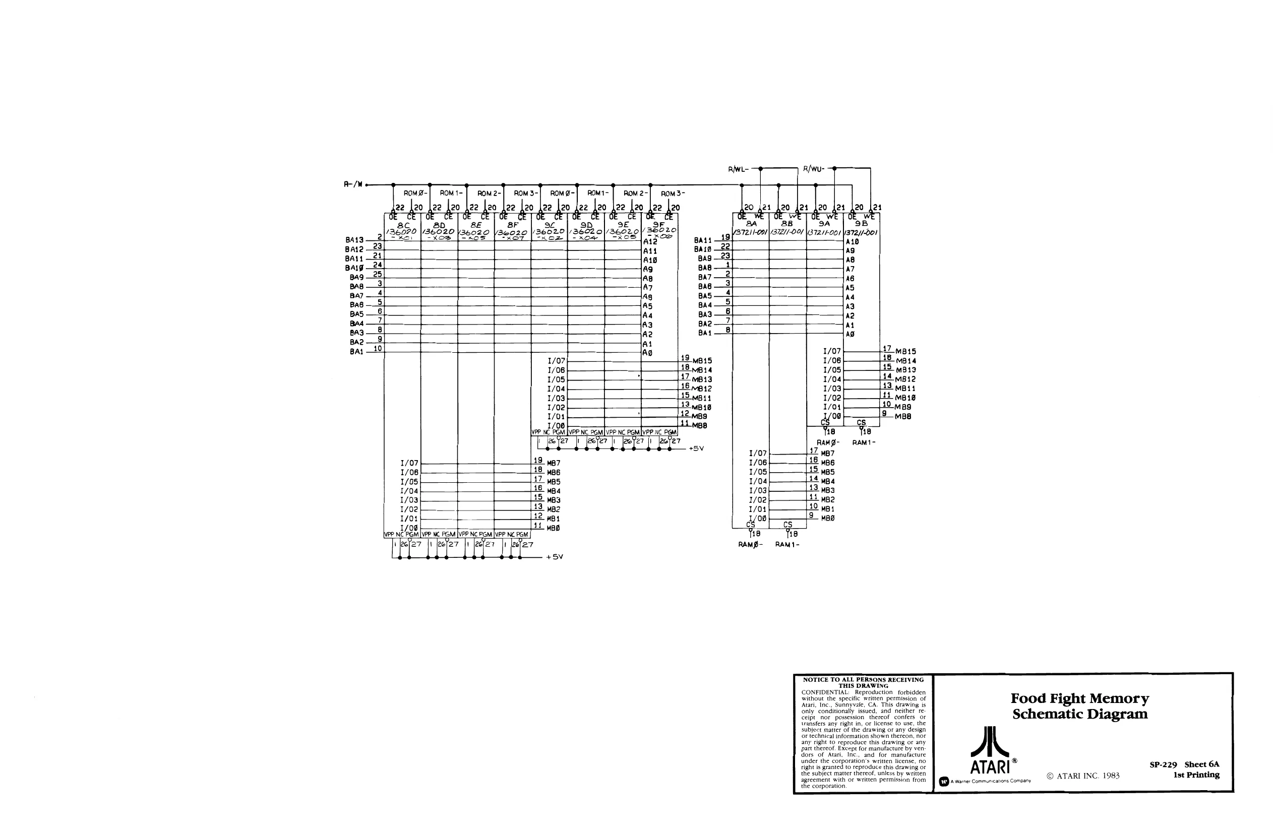
This page is a drawing, shown as the original scan.
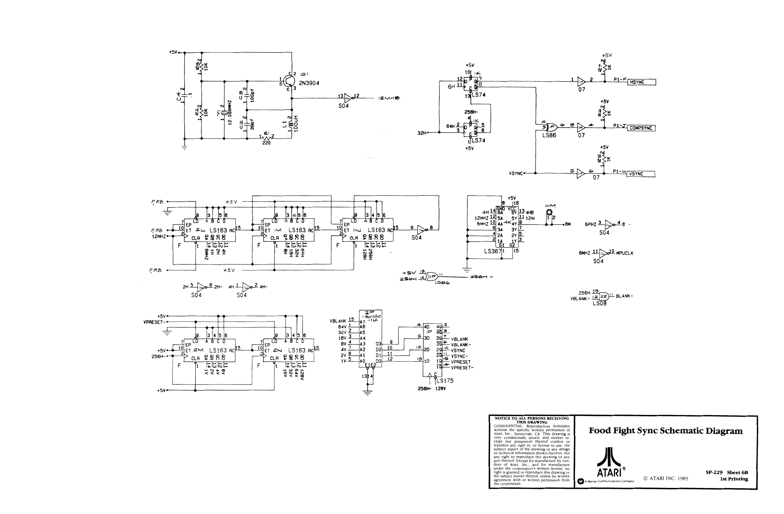
This page is a drawing, shown as the original scan.
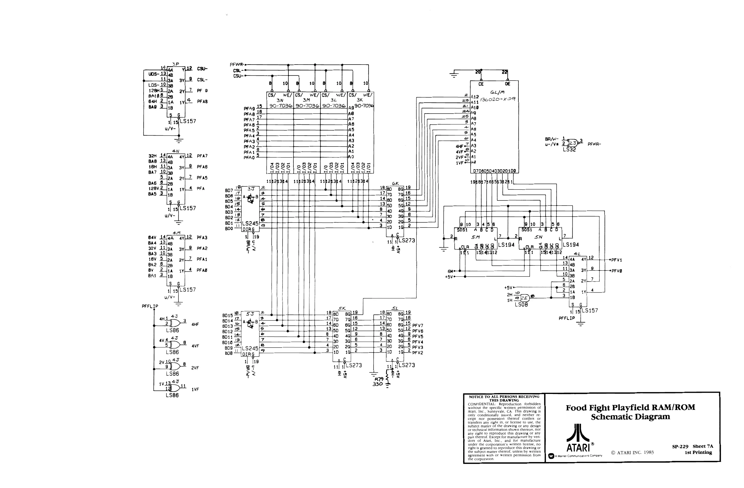
This page is a drawing, shown as the original scan.
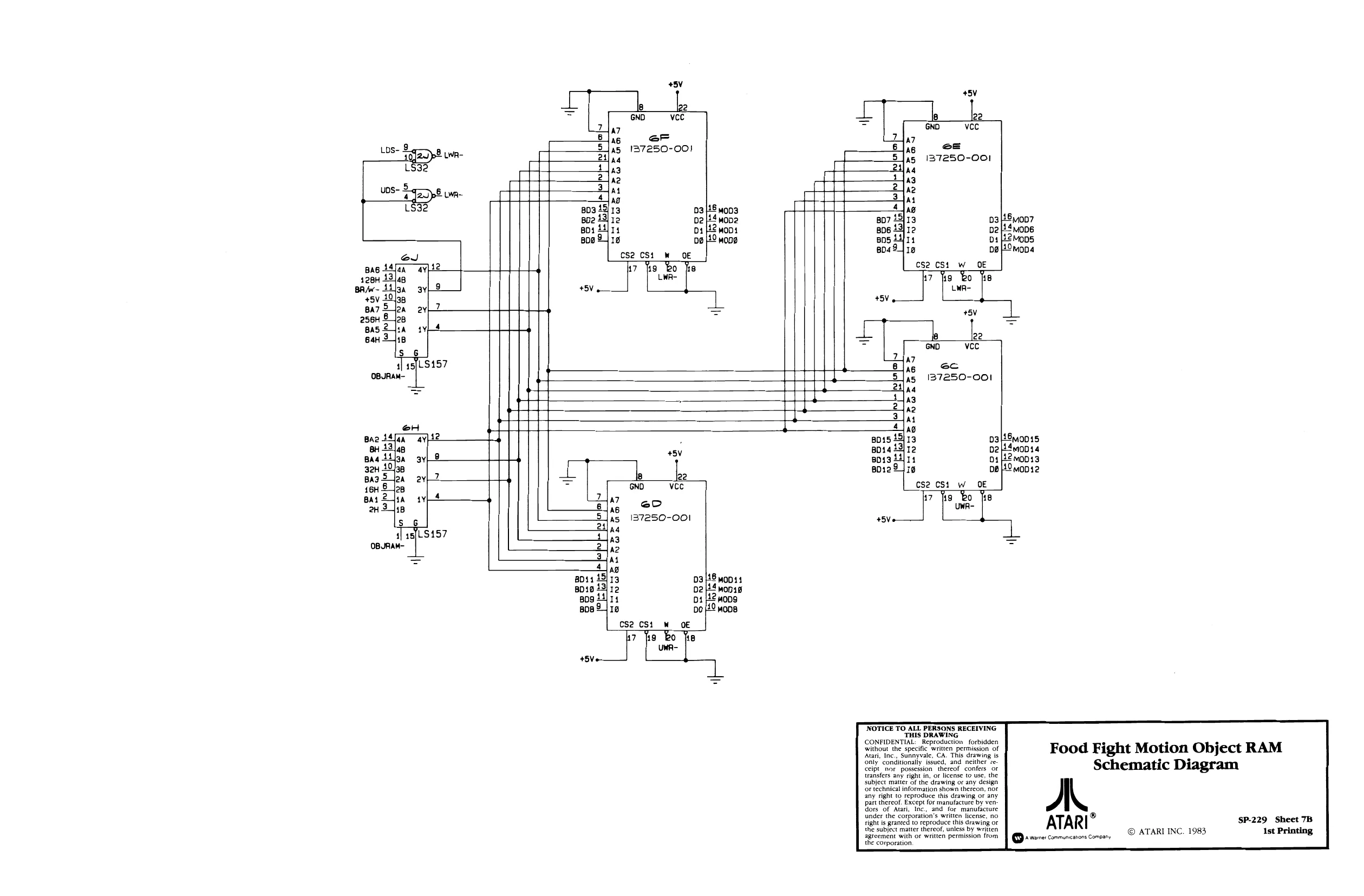
This page is a drawing, shown as the original scan.
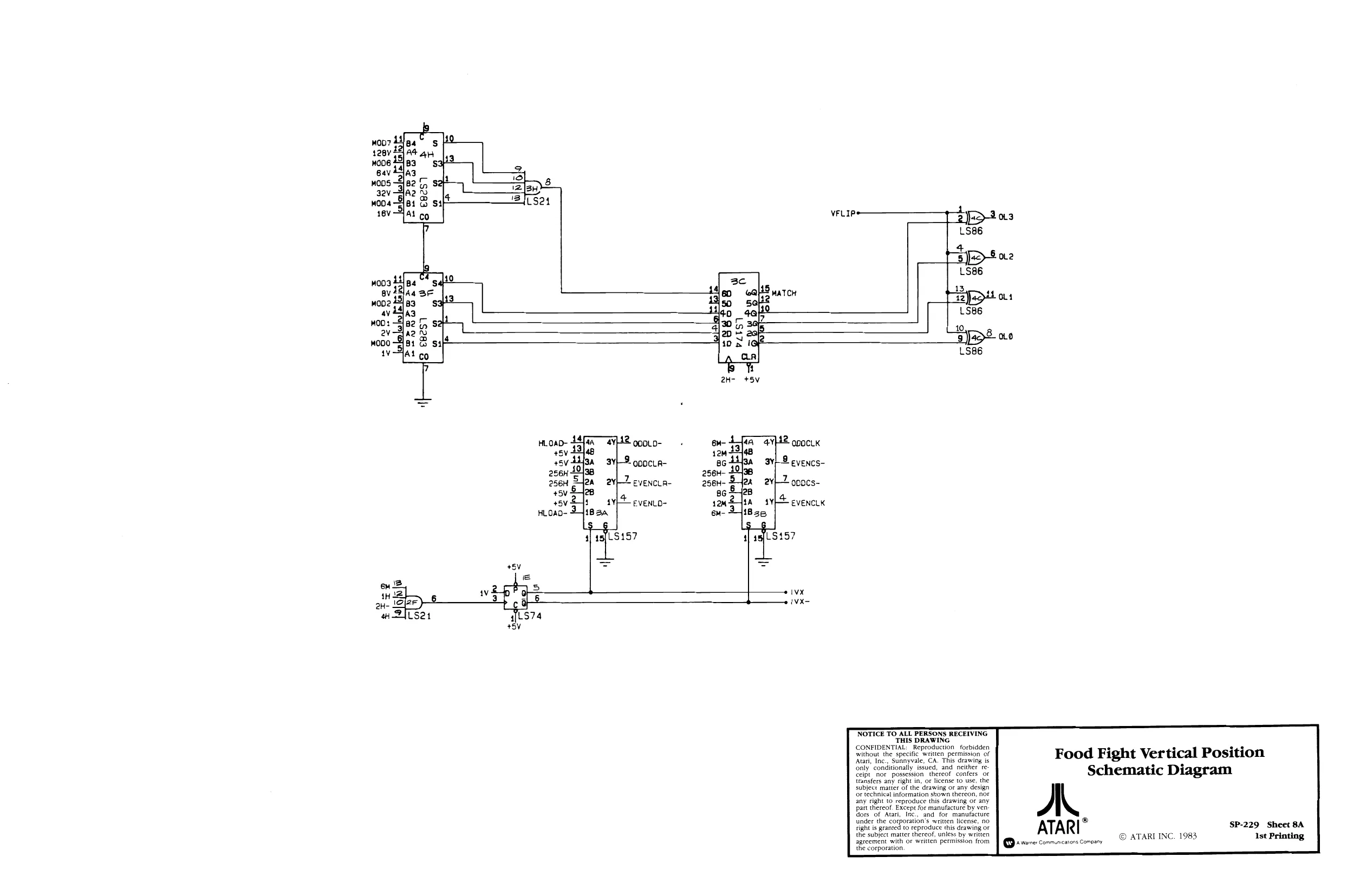
This page is a drawing, shown as the original scan.
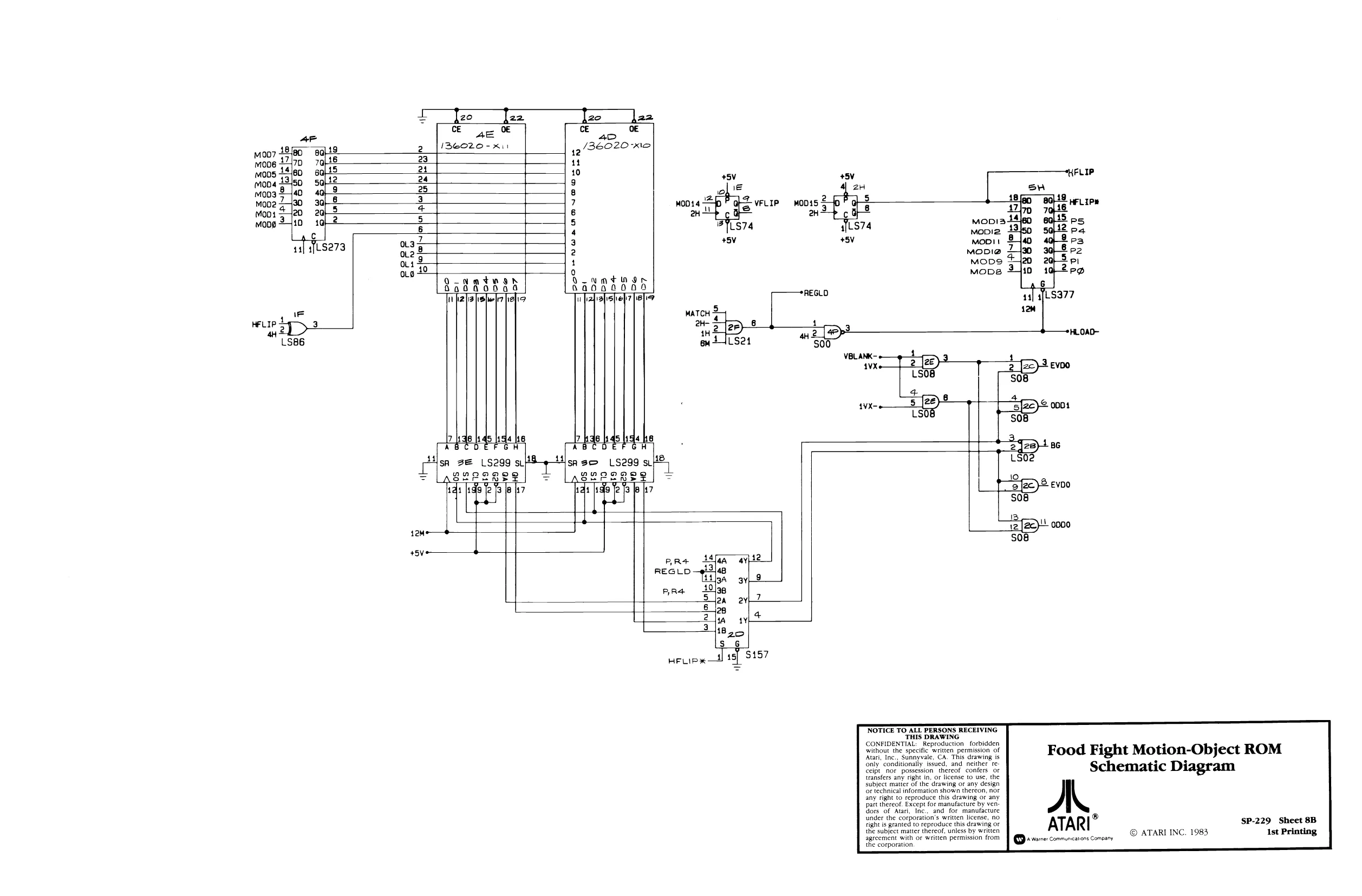
This page is a drawing, shown as the original scan.
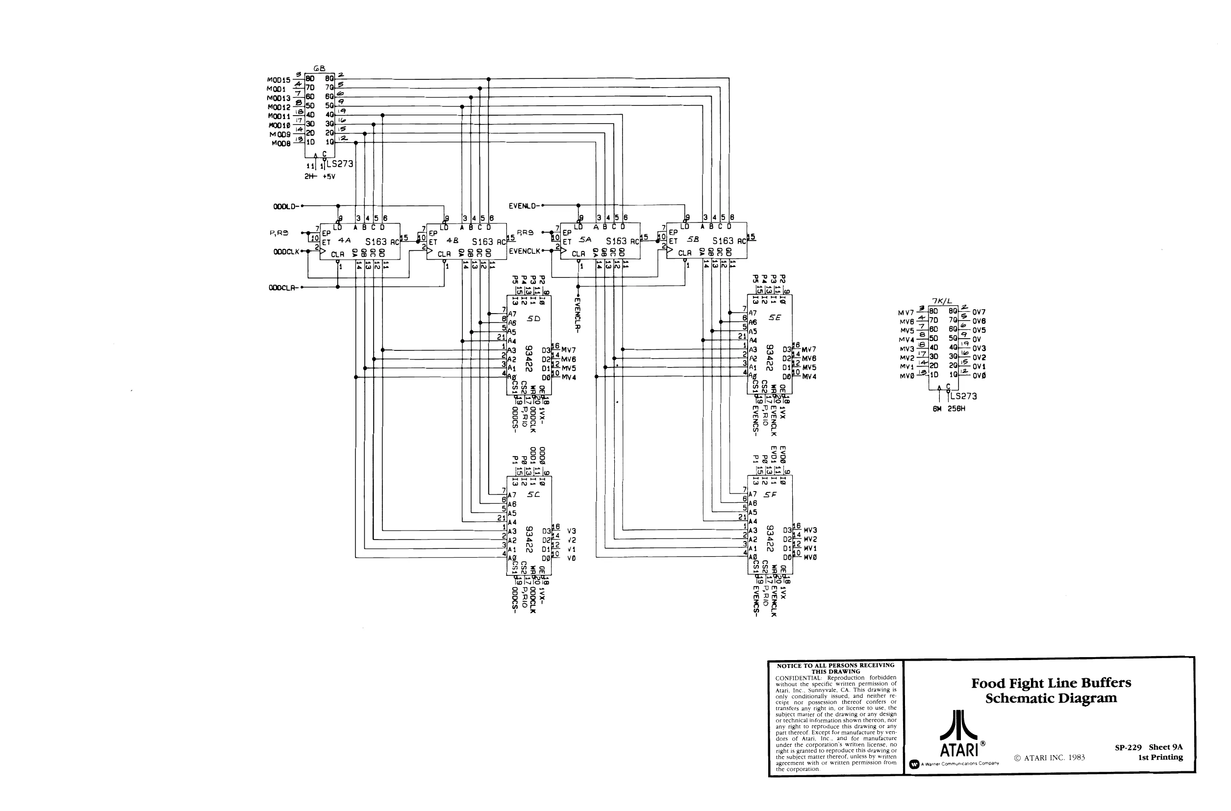
This page is a drawing, shown as the original scan.
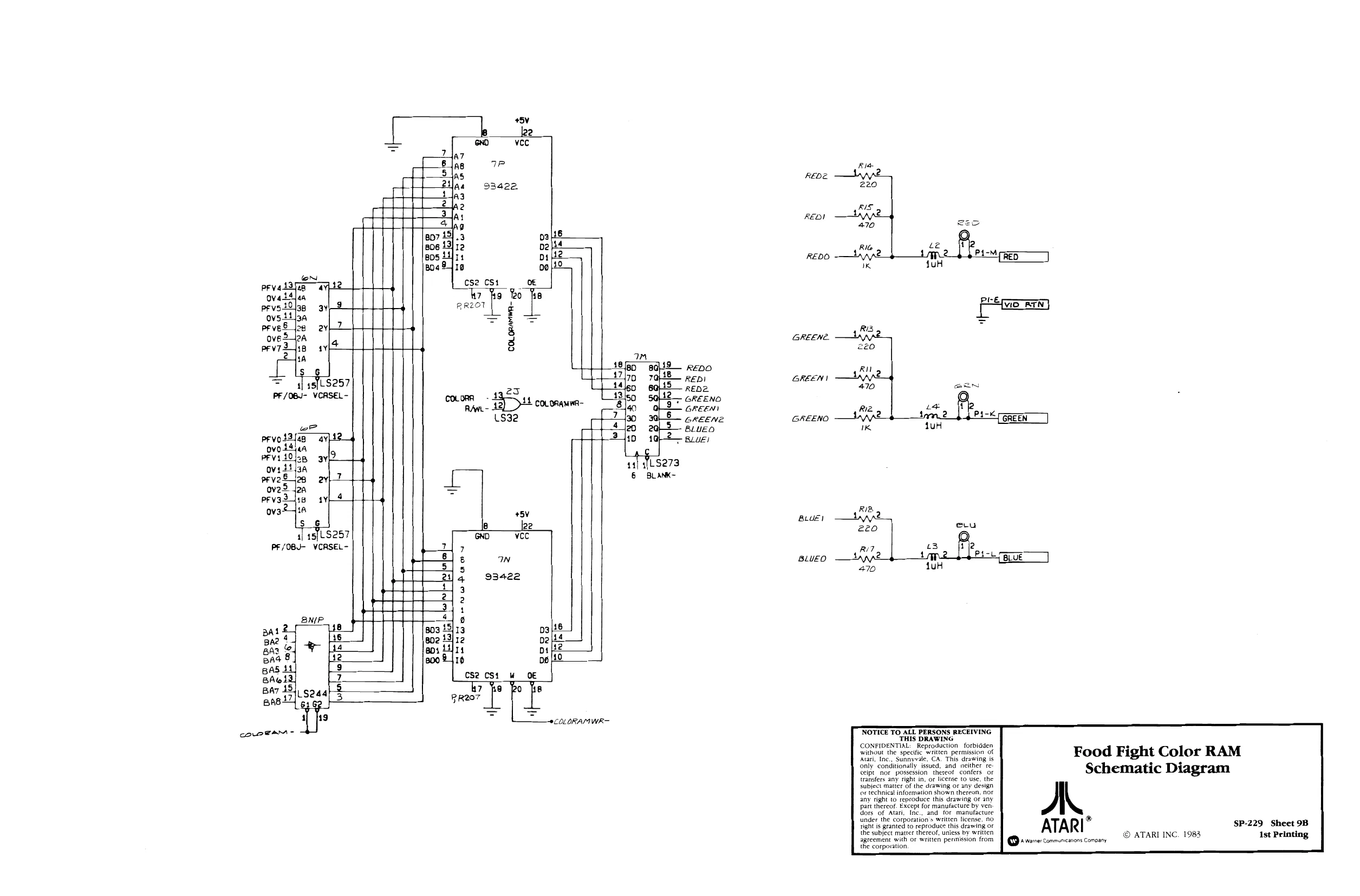
This page is a drawing, shown as the original scan.
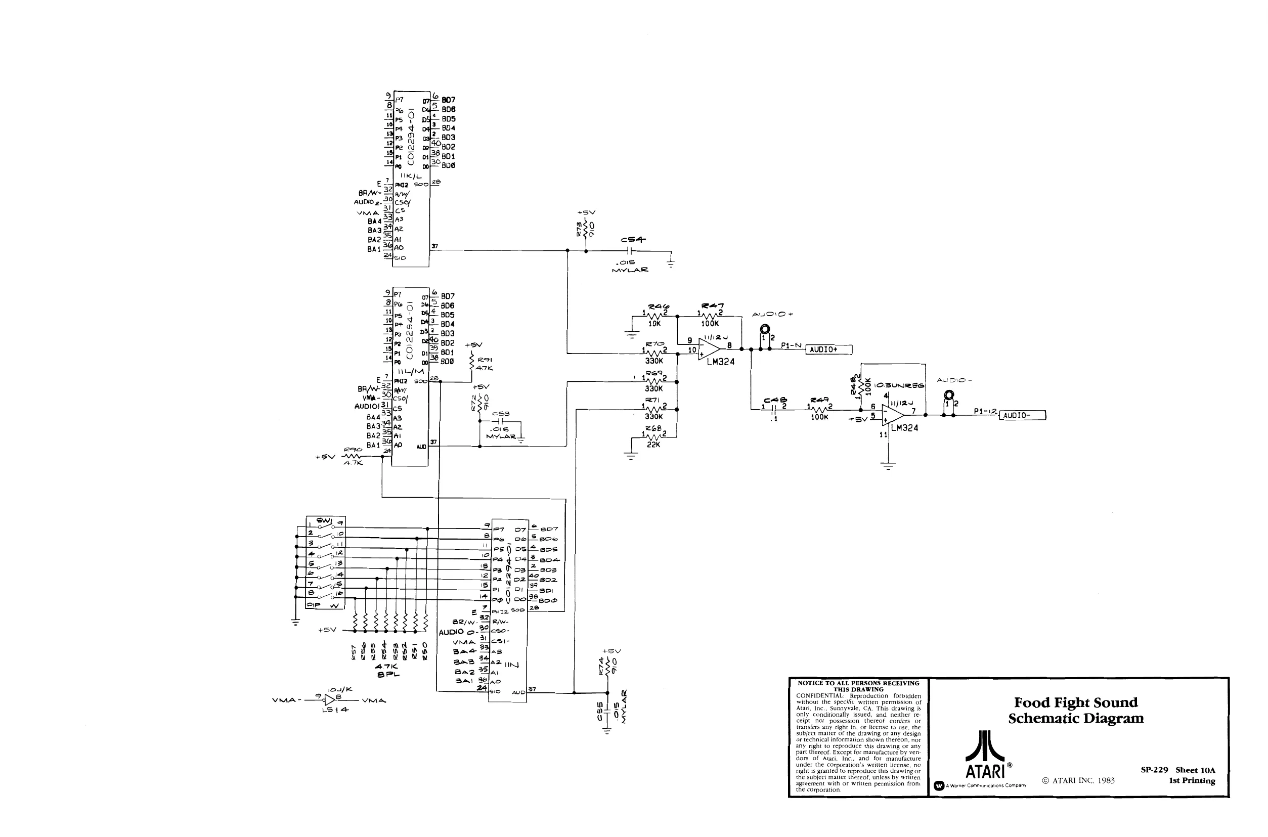
This page is a drawing, shown as the original scan.
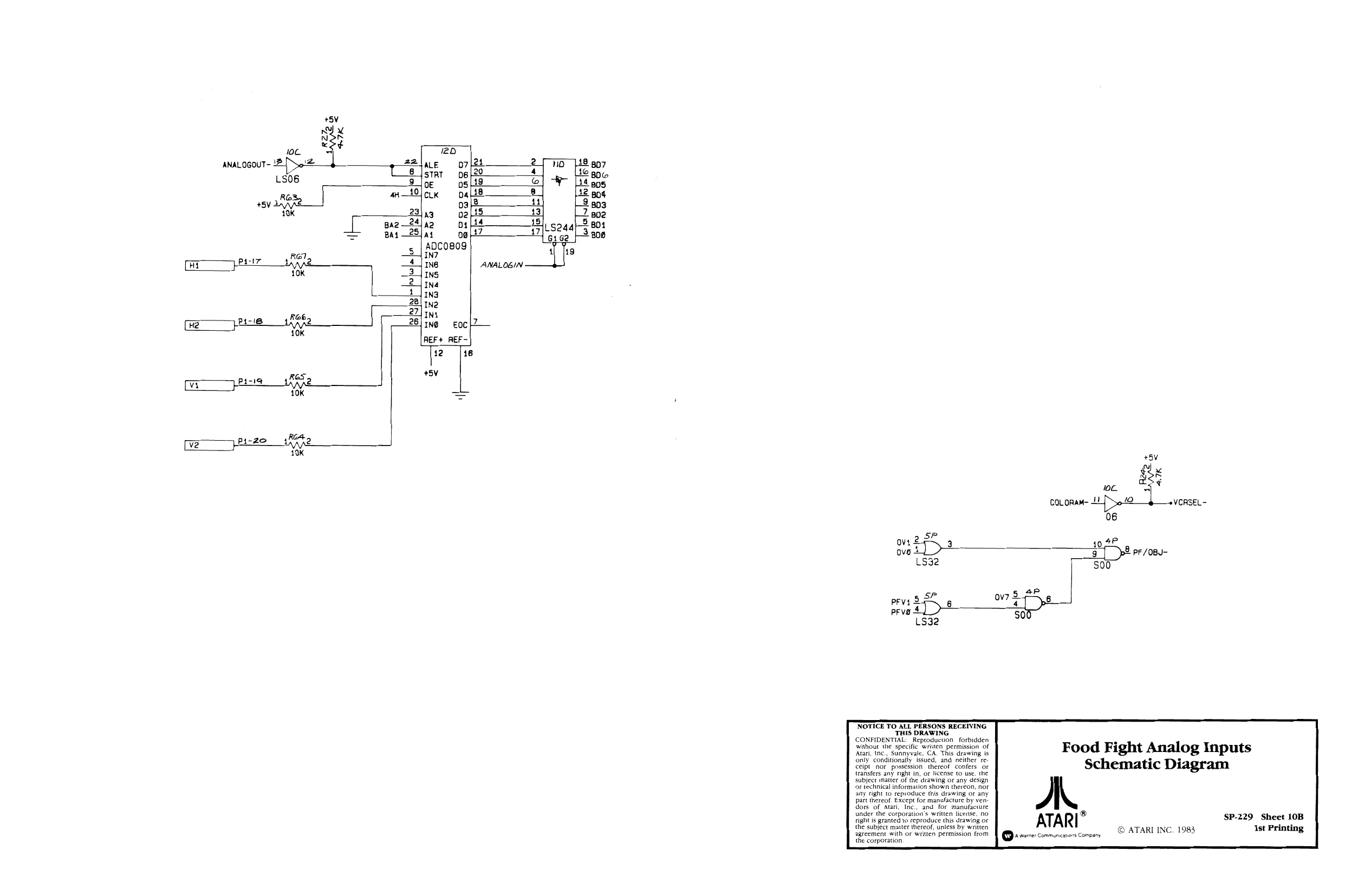
This page is a drawing, shown as the original scan.
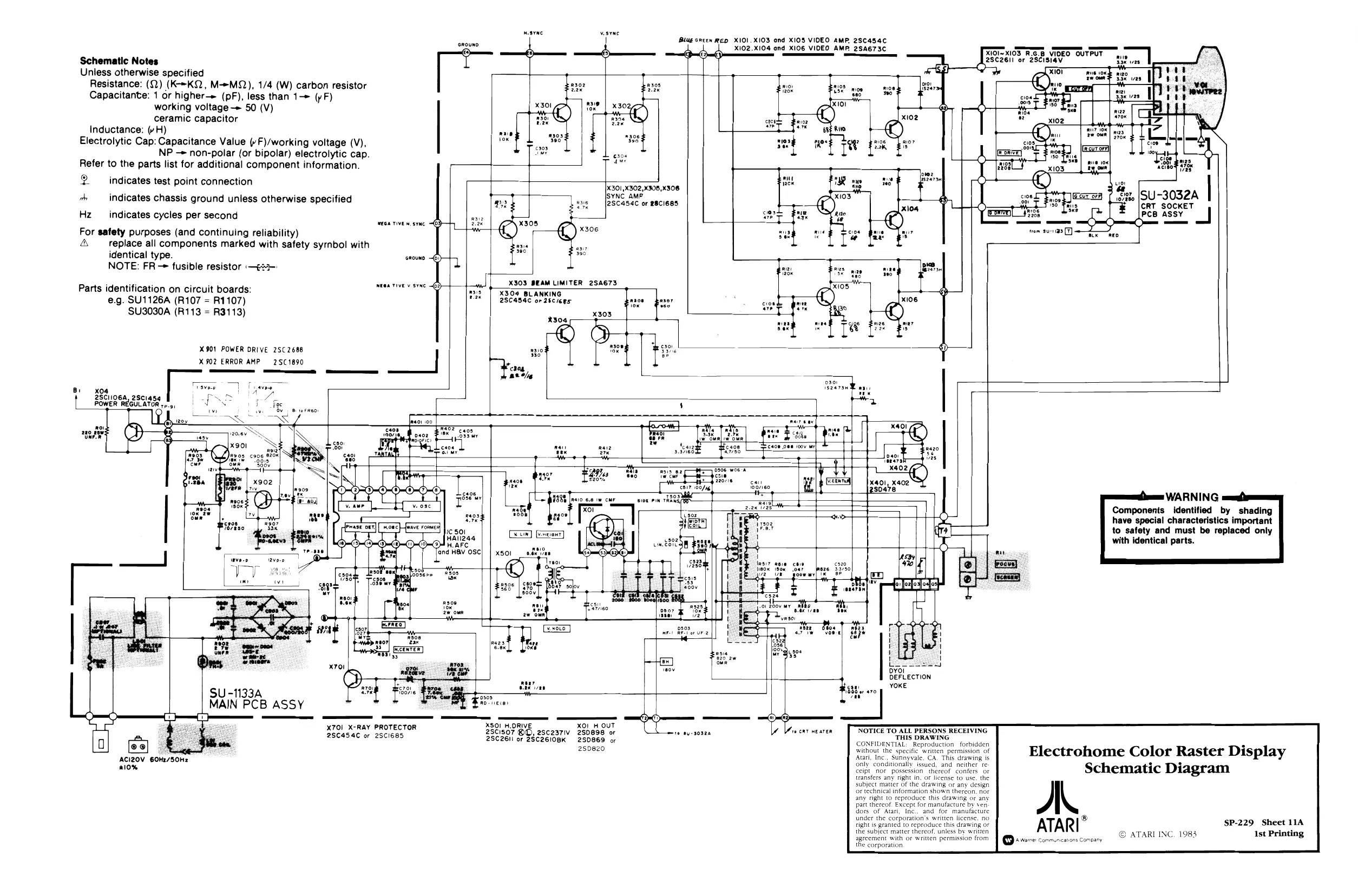
weayne vesyme Blug cneen RED XIO1.X103 and X105 VIDEO AMP, 28¢454C
| GROUND | \ | d | X102.X104 and X1I06 VIDEO AMP. 2SA673C |
Schematic Notes ; : Unless otherwise specified Resistance: (Q) (K->KQ, M->MQ2), 1/4 (W) carbon resistor hes TS? noe Capacitante: 1 or higher—> (pF), less than 1-~ (yF) working voltage -» 50 (V) ceramic capacitor Inductance: (vH) ane Electrolytic Cap: Capacitance Value (F)/working voltage (V), a NP - non-polar (or bipolar) electrolytic cap. Refer to the parts list for additional component information. 2 indicates test point connection hn indicates chassis ground unless otherwise specified X10l=x103 RGB VIDEO OUTPUT 4, 2SC26II or 28CIS14V vas
X301 ,X302,x308,x308 SYNC AMP. 2SC454C or BBCI685 ISU-3032A | ICRT SOCKET PCB ASSY Hz indicates cycles per second
| ween riven sinc | GS | x305 |
For satety purposes (and continuing reliability) © X08
a replace all components marked with safety syrnbol with * gy
identical type.
X901 POWER DRIVE 25C2688 X02 ERROR AMP —2S( 1890
x04 2SCi106A, 2sci4s¢ POWER REGULATOR rp.9,
= WARNING
2.201 Components identified by shading
rreg have special characteristics important ay tae to safety and must be replaced only
| we! | Halizea | t | 1 | with identical parts. |
| . | and HAV 0sc| | oben | re | | |
| on | TE | oy ae ous | ||
| E Tait dt | =| | ay | | ||{i | |
| a | | | L | 1 |
meor) "zane i Beran
mS 820 2w
| Lie] | a | be |
ares, eat = BerLection
| = | Oe | YOKE |
SU-1133A te * MAIN PCB ASSY ee
| % | X7O1 X-RAY PROTECTOR | eb RS, ascosriv Bheds ur | asi | Te ORT EATER | ‘NOTICE TO ALL PERSONS RECEIVING |
| : | or | ne usa | ‘THIS DRAWING | ||
| ; | 2SC454C or 25ci685 | 28C261i or ZSC2EIOBK | 250869 or | CONFIDENTIAL: Reproduction forbidden |
ExS 280820 without the specific weitten permission of
Electrohome Color Raster Display
Schematic Diagram
ATARI : SP-229 Sheet 11A
°o co © ATARI INC. 1983 Ist Printing
Atari, Inc., Sunnyvale, CA. This drawing is only conditionally issued, and neither re Ceipt_nor possession thereof confers or transfers any right in, of license to use. the subject matter Of the drawing or any design or technical information shown thereon. nor any right to reproduce this drawing or any part thereof Except for manufacture by ven dors of Atari, Inc. and for manufacture ACI20V 6OH2/50H2 210%
tnder the corporation's written license, no right is granted to reproduce this drawing or the subject mater thereo. uness by writen agreement with or written permission from the corporation,
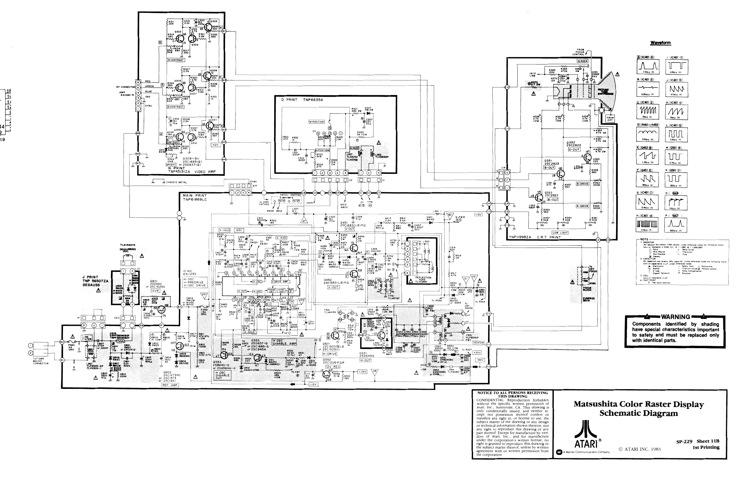
This page is a drawing, shown as the original scan.