Major Havoc SP-252 2nd Printing
Major Havoc (rev 3) (Atari, 1983) · Schematic Package · 19 pages · 49 sections · original scan
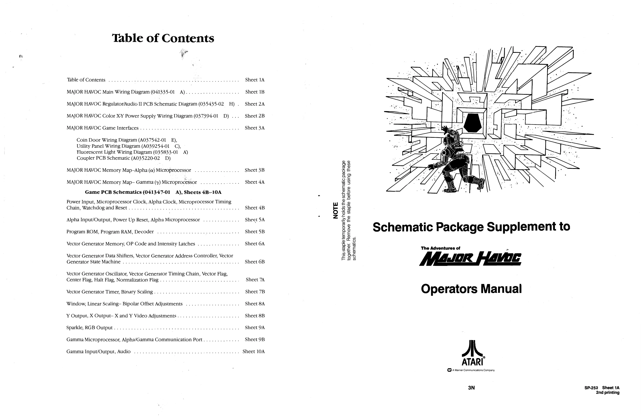
Table of Contents
Table of Contents Sheet 1A
MAJOR HAVOC Main Wiring Diagram (041335-01 A)......-..-...-55 .. Sheet 1B
MAJOR HAVOC Regulator/Audio II PCB Schematic Diagram (035435-02 H) . Sheet 2A
MAJOR HAVOC Color XY Power Supply Wiring Diagram (037394-01 D) ... Sheet 2B
MAJOR HAVOC Game Interfaces .......... seen a kee untae mete ge eo oan Sheet 3A
Coin Door Wiring Diagram (A037542-01 E), Utility Panel Wiring Diagram (A039254-01 C), Fluorescent Light Wiring Diagram (035833-01 A) Coupler PCB Schematic (A035220-02 D)
MAJOR HAVOC Memory Map-Alpha (a) Microprocessor Sheet 3B
MAJOR HAVOC Memory Map- Gamma (y) Microprocessor nes Sheet 4A Game PCB Schematics (041347-01 A), Sheets 4B--10A
Power Input, Microprocessor Clock, Alpha Clock, Microprocessor Timing Chain, Watchdog and Reset........... ease dade amare Lemmas 3 Hw Sheet 4B
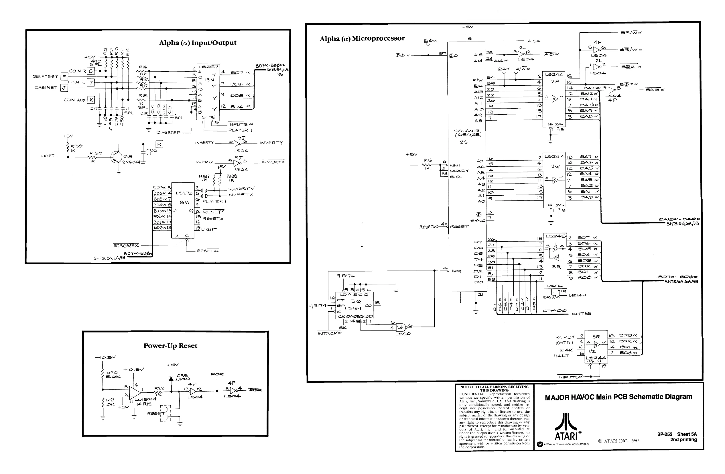
Alpha Input/Output, Power Up Reset, Alpha Microprocessor ............. Sheet SA
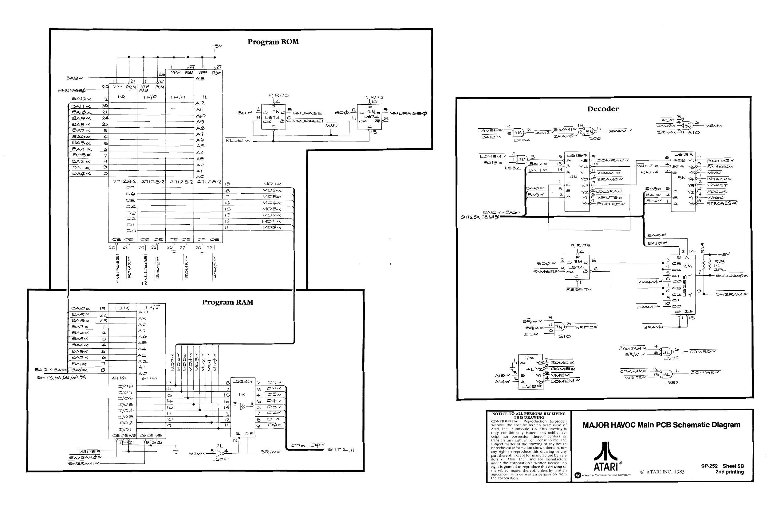
Program ROM, Program RAM, Decoder .............. 00 ccc eeeee eee Sheet 5B
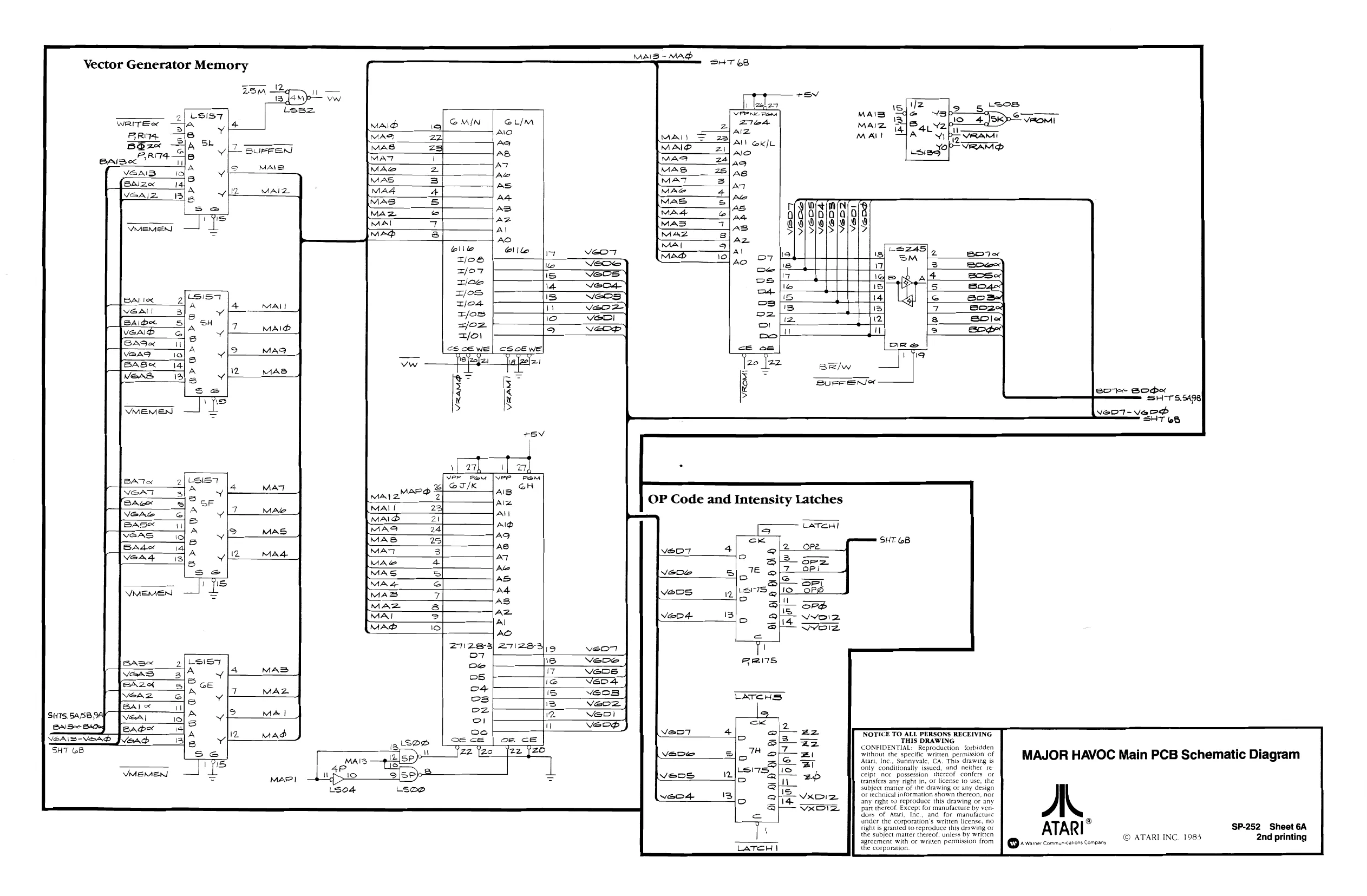
Vector Generator Memory, OP Code and Intensity Latches ..........-...+ Sheet 6A
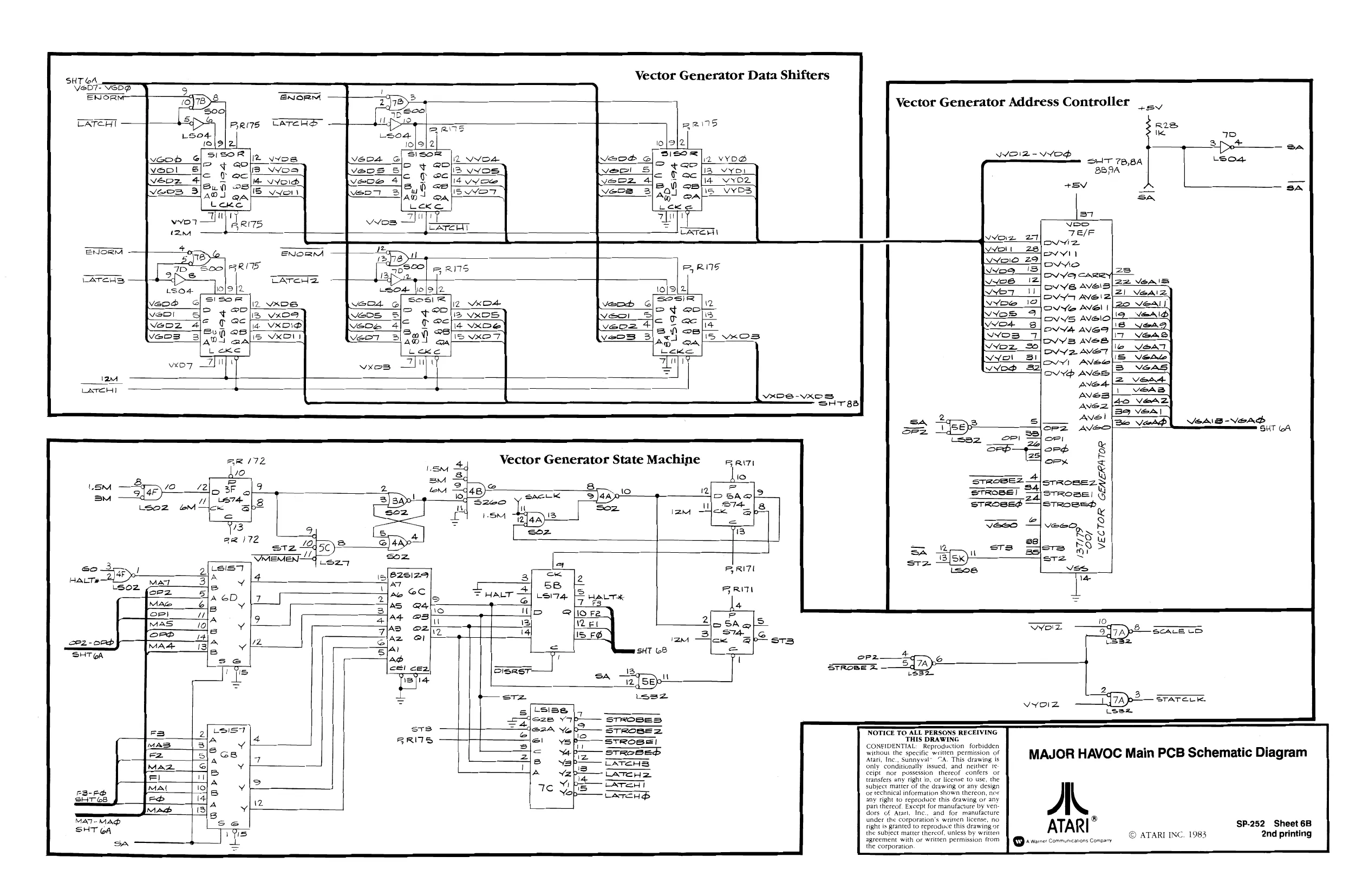
Vector Generator Data Shifters, Vector Generator Address Controller, Vector Generator State Machine ...............00.200005 enn Sheet 6B
Vector Generator Oscillator, Vector Generator Timing Chain, Vector Flag, Center Flag, Halt Flag, Normalization Flag............. 000000 Sheet 7A
Vector Generator Timer, Binary Scaling... .... 00.60. e eee eee eee Sheet 7B
Window, Linear Scaling— Bipolar Offset Adjustments ..............05 + Sheet 8A
Y Output, X Output- X and Y Video Adjustments ............ sees Sheet 8B
Sparkle, RGB Output......... ene eee een eee nena seveeesee. Sheet 9A Gamma Microprocessor, Alpha/Gamma Communication Port........ . ... Sheet 9B
Gamma Input/Output, Audio Sheet 10A
schematics. Schematic Package Supplement to
The Adventures of [+144 [4
Operators Manual
ATARI (9 A Warner Commurictons Company
3N SP.252 Sheet 1A 2nd printing
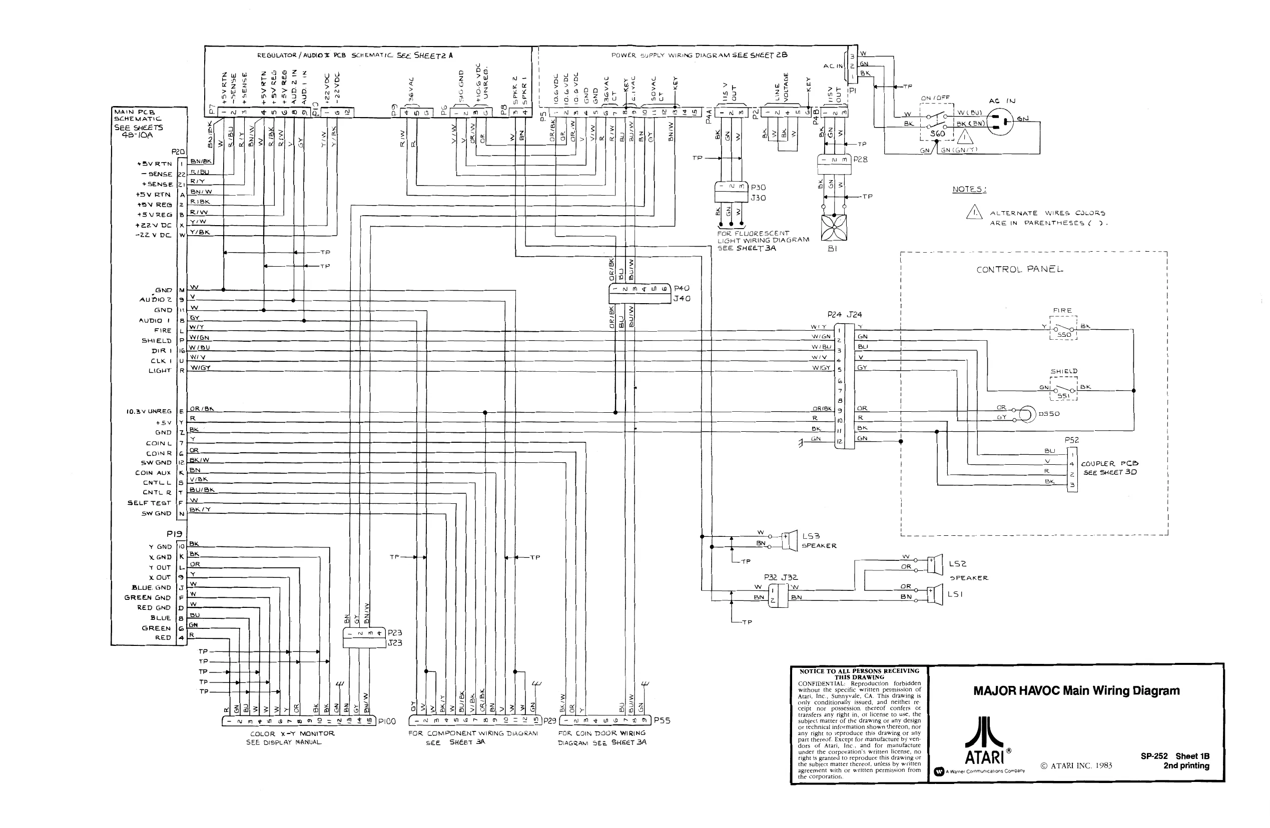
This page is a drawing, shown as the original scan.
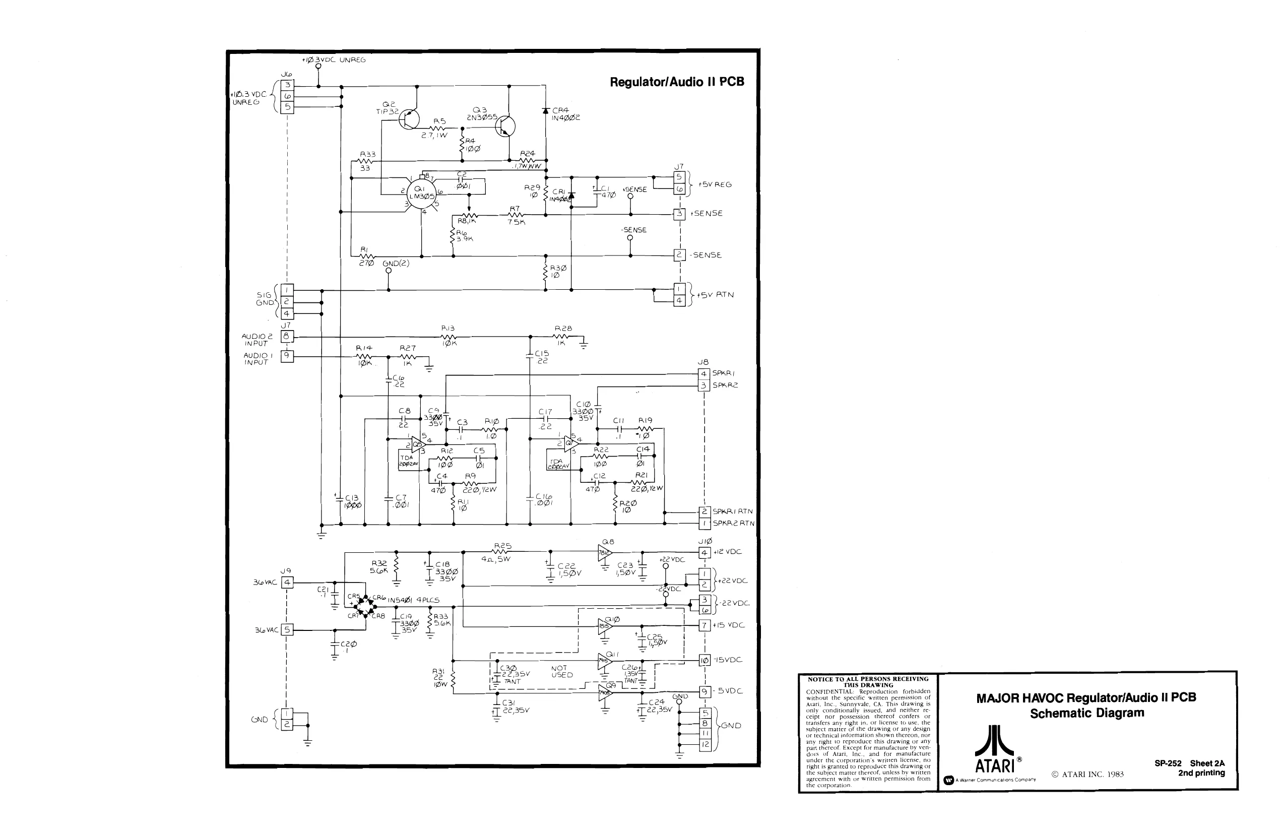
This page is a drawing, shown as the original scan.
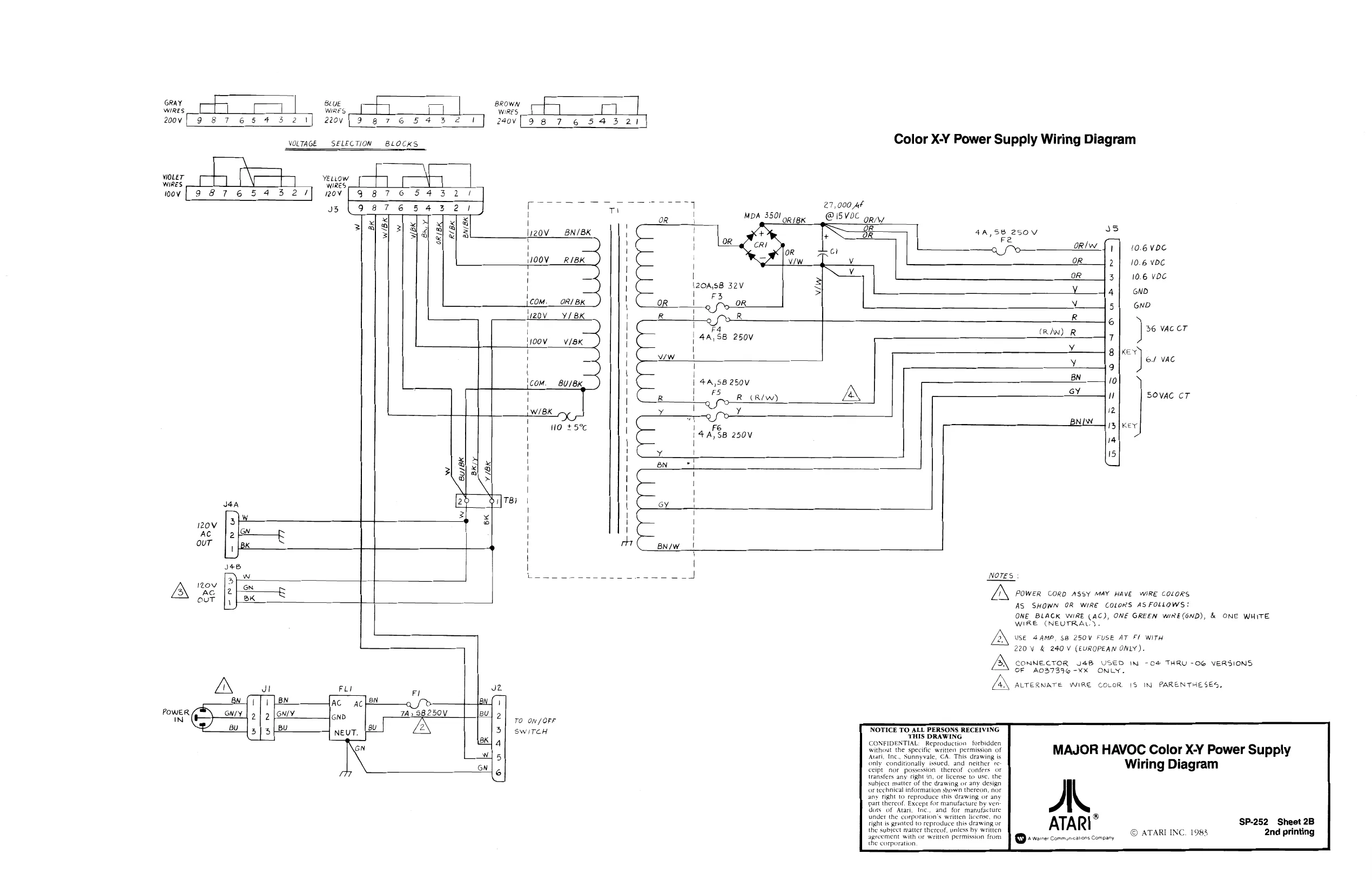
This page is a drawing, shown as the original scan.
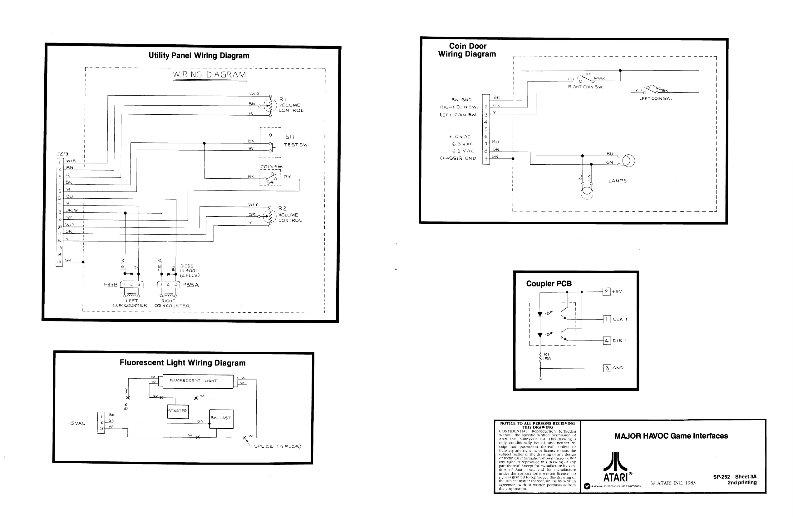
Coin Door
Utility Panel Wiring Diagram Wiring Diagram
WIRING DIAGRAM
or ¢ NOB K 28 % IGHT COINS Qh RIG Sw yo NO
sw 6ND < LEFT COINSW.
RIGHT COIN SW
LEFT COIN SW
+1OVDC
6.3 VAC
63 VAC
CHASSIS. GND
VOLUME, CONTROL
| DI00E a iN 4001 (2PLcs) 12 3) PaSA Coupler PCB
LEFT RIGHT COINCOUNTER — COINCOUNTER
Fluorescent Light Wiring Diagram
wi FLUORESCENT
\ISVAC NOTICE TO ALL PERSONS RECEIVING "HS DRAWING nn CONFIDENTIAL. Reproduction forbidde oa ind sie specie ween pasion of MAJOR HAVOC Game Interfaces SPLICE (5 PLCS) trabafery anf ight Inv or ikente FO Use, the subject matter of the drawing or any design
or technical information shown thereon, nor
any right to reproduce this drawing or any part thereof. Except for manufacture by ven ors of Atari, Ine.. and for manufacture under the curporation’s written license, no, ® fa i grated o eprodce this drawing or ATARI . ; SP-252 Sheet 3A
the subject matter thereot. unless by writer © ATARI INC. 1983 2nd printing
eK x
BALLAST en
Ww x
\
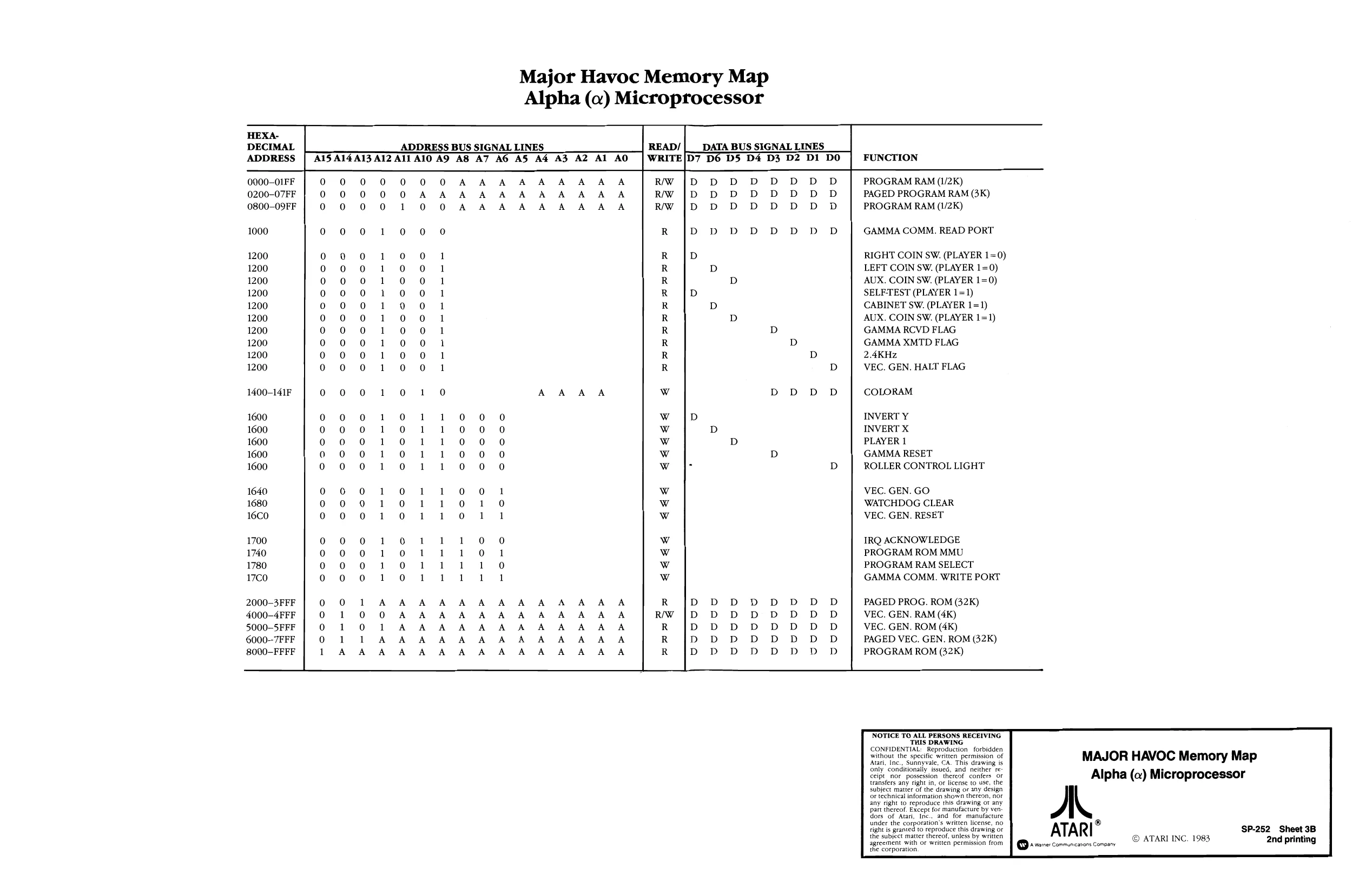
Major Havoc Memory Map Alpha (a) Microprocessor
HEXA- DECIMAL ADDRESS BUS SIGNAL LINES READ/
| 0000-O1FF | 0 0 00 00 0 A AA AA A A AA | RW IDDDDDODOD OD | PROGRAM RAM (1/2K) | ||
| 0200-07FF | 0 0 0 0 0 A A A A A A AA AAA | RW | DDODODODOD OD | PAGED PROGRAM RAM (3K) | |
| 0800-09FF | 0 0 0 0 10 0 A A A A A A A AA | RW ID DD DDODOD OD | PROGRAM RAM (1/2K) | ||
| 1000 | o 0 0 10 0 0 | R | DD ODODODOD OD | GAMMA COMM. READ PORT | |
| 1200 | o 0 0 10 0 1 | R | RIGHT COIN SW. (PLAYER 1=0) | ||
| 1200 | 0 0 0 100 1 | R | D | LEFT COIN SW. (PLAYER 1=0) | |
| 1200 | 0 0 0 10 0 1 | R | D | AUX. COIN SW. (PLAYER 1=0) | |
| 1200 | oo 0 10 0 1 | R | SELF-TEST (PLAYER 1=1) | ||
| 1200 | o 0 0 10 0 1 | R | D | CABINET SW. (PLAYER 1=1) | |
| 1200 | 0 0 0 10 0 1 | R | D | AUX. COIN SW. (PLAYER 1=1) | |
| 1200 | 0 0 0 10 0 1 | R | D | GAMMA RCVD FLAG | |
| 1200 | 0 0 0 10 0 1 | R | D | GAMMA XMTD FLAG | |
| 1200 | 0 0 0 10 0 1 | R | D | 2.4KHz | |
| 1200 | 0 0 0 10 0 1 | R | D | VEC. GEN. HALT FLAG | |
| 1400-141F | 0 0 0 10 1 0 | A A A A | Ww | DOD OD OD | COLORAM |
| 1600 | 0 0 0 1 0 1 1 0 0 0 | Ww | INVERT Y | ||
| 1600 | 0 0 0 10 1 1 0 0 0 | Ww | D | INVERT X | |
| 1600 | oo 0 1 0 1 1 0 0 0 | Ww | D | PLAYER 1 | |
| 1600 | o 0 0 10 1 1 0 0 0 | Ww | D | GAMMA RESET | |
| 1600 | 0 0 0 1 0 1 1 0 0 0 | Ww | D | ROLLER CONTROL LIGHT | |
| 1640 | 0 6 0 1 0 1 | 1 ~°0 | 1 | Ww | VEC. GEN. GO |
| 1680 | 0 0 90 1 0 1 1 0 1 0 | Ww | ‘WATCHDOG CLEAR | ||
| 16CO | 0 0 0 1 01 1 01 1 | Ww | VEC. GEN. RESET | ||
| 1700 | 0 0 0 1 0 1 21 21 0 0 | w | IRQ ACKNOWLEDGE | ||
| 1740 | 0 0 0 10 1 | 1 1 01 | Ww | PROGRAM ROM MMU | |
| 1780 | 0 0 0 1 0 1 21 21 1 «0 | Ww | PROGRAM RAM SELECT | ||
| 170 | ooo 1 0 1 1 21 | 21 | «21 | Ww | GAMMA COMM. WRITE PORT |
| 2000-3FFF | o 0 1 A A A AA A A A A A AAA | R | DDD ODODOD OD | PAGED PROG. ROM (32K) | |
| 4000-4FFF | o 1 00 AA A A AA A A AA AA | RW | DDDoDODOD OD | VEC. GEN. RAM (4K) | |
| 5000-5FFF | o 101 AA A A A AA A A AAA | R | DDODODOD OD OD | VEC. GEN. ROM (4K) | |
| 6000--7FFF | 0 1 | 1 A A A A A A A AK A A AAA | R | DDD DOD OD D | PAGED VEC. GEN. ROM (32K) |
| 8000-FFFF | 1 A A A A A A A A A A A A A AA | DDODODOD OD D | PROGRAM ROM (32K) |
CoNIDENTIAL Reproduction, Cte A sous espa maton permeton MAJOR HAVOC Memory Map Ceipt ‘nor possession thereof confers or Alpha (a) Microprocessor transfers any right in, or license to use, the subject matter of the drawing or any design, or technical information shown thereon, nor any right to reproduce this drawing ot any part thereof. Except for manufacture by ven: dors of Atari, Inc., and for manufacture sn car rt ATARI® sP-252 sheet 38 Ine subject matter thereof, unless by wien © ATARI INC. 1983 2nd printing
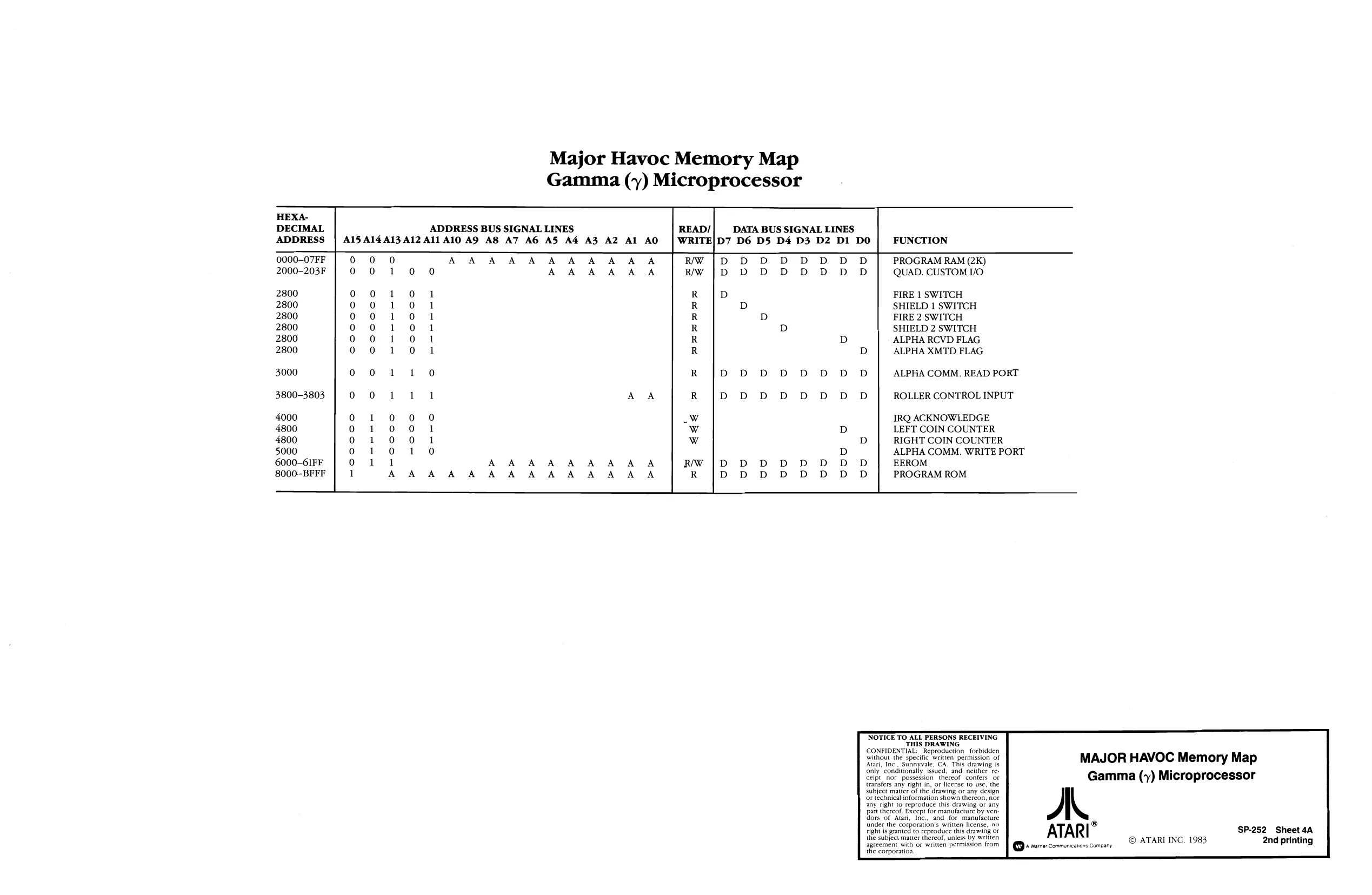
Major Havoc Memory Map Gamma (y) Microprocessor
HEXA-
DECIMAL ADDRESS BUS SIGNAL LINES DATA BUS SIGNAL LINES
| ADDRESS | A15 A14A13 Al2 All A10 A9 A8 A7 A6 A5 A4 AZ AZ Al AO | D7 D6 D5 D4 D3 D2 Di DO | FUNCTION | |||||||||||
| 0000-07FF | 6 | 0 | 0 | A | A | A | A | A | A | A | A | A | AA | PROGRAM RAM (2K) |
| 2000-203F | o | 0 | 1 | 0 | 0 | A | A | A | A | A | A | RW | QUAD. CUSTOM I/O | |
| 2800 | oo | 1 | 0 | 1 | R | D | FIRE 1 SWITCH | |||||||
| 2800 | o | 0 | 1 | 0 | 1 | R | D | SHIELD 1 SWITCH | ||||||
| 2800 | 0 | 0 | 10 | 1 | R | D | FIRE 2 SWITCH | |||||||
| 2800 | 0 | 0 | 10 | 1 | R | D | SHIELD 2 SWITCH | |||||||
| 2800 | oo1 | 01 | R | D | ALPHA RCVD FLAG | |||||||||
| 2800 | oo | 1 | 0 | 1 | R | D | ALPHA XMTD FLAG | |||||||
| 3000 | o | o | 1 | 1 | 0 | R | D | D | ALPHA COMM. READ PORT | |||||
| 3800-3803 | 0 | 0 | 1 | 1 | 1 | A | A | ROLLER CONTROL INPUT | ||||||
| 4000 | 0 | 1°00 | 0 | IRQ ACKNOWLEDGE | ||||||||||
| 4800 | o | 100 | 1 | LEFT COIN COUNTER | ||||||||||
| 4800 | o | 10 | 01 | RIGHT COIN COUNTER | ||||||||||
| 5000 | o | 1 | 0 | 1 | 0 | ALPHA COMM. WRITE PORT | ||||||||
| 6000-61FF | o | 11 | A | A | A | A | A | A | A | A | A | EEROM | ||
| 8000-BFFF | 1 | A | A | A | A | A | A | A | A | A | A | A | AAA | PROGRAM ROM |
"NOTICE TO ALL PERSONS RECEIVING THIS DRAWING CONFIDENTIAL: Reproduction forbidden Munna Sabagrse” Co TRS Gane MAJOR HAVOC Memory Map cele ‘nor porsession thereof confers. oF Gamma (7) Microprocessor transfers any right in, or license 10 use, the subject matter of the drawing or any design ‘or technical information shown thereon, nor any right to reproduce this drawing or any part thereof, Except for manufacture by ven: dors of Atari, Inc., and for manufacture sais teae orca sug ATARI® $P-252 Sheet 4a greement vath or watten permision £0" | @) pane: commons Conoary the corporation, © ATARI INC. 1983 2nd printing
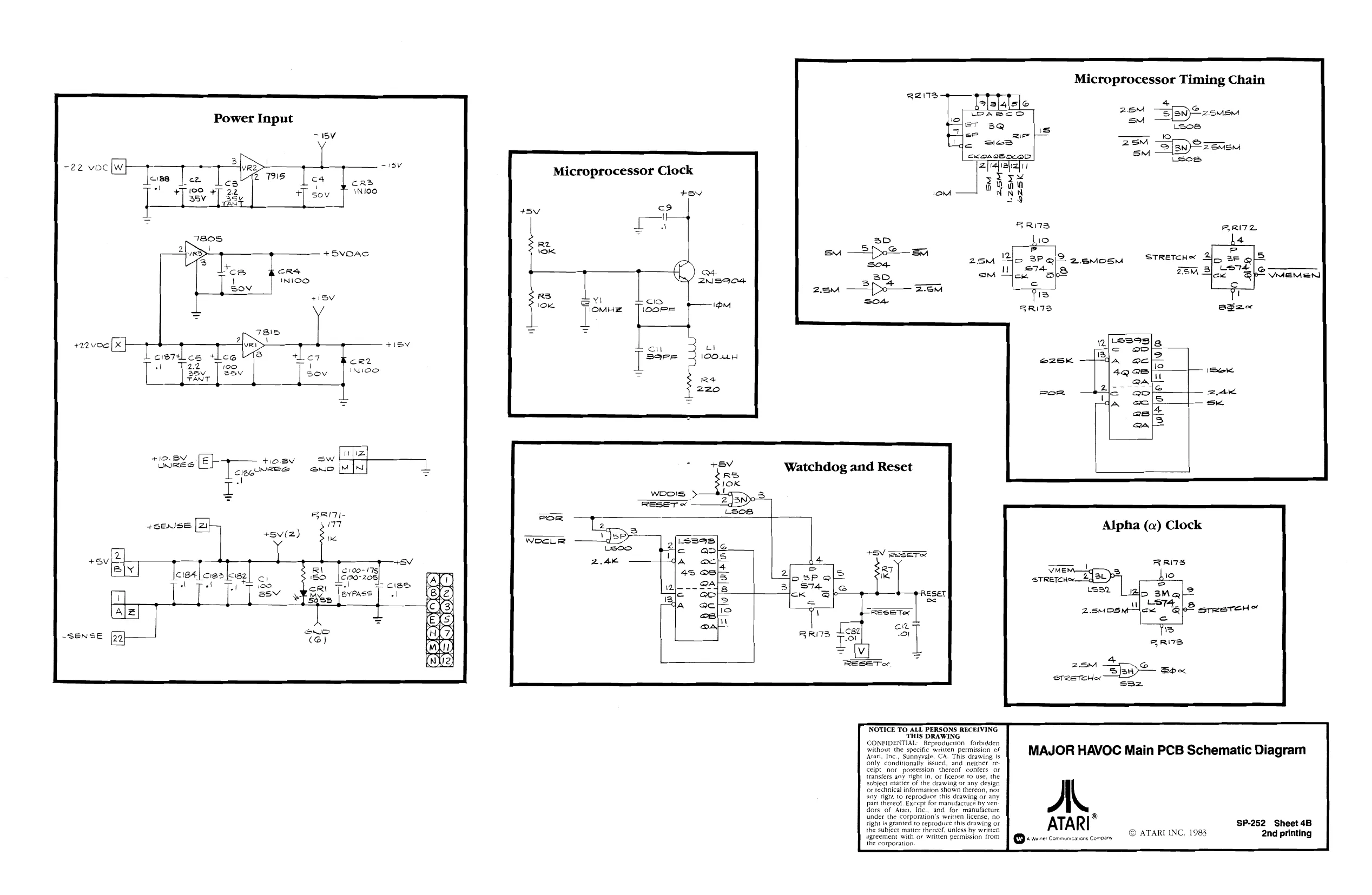
This page is a drawing, shown as the original scan.
This page is a drawing, shown as the original scan.
This page is a drawing, shown as the original scan.
This page is a drawing, shown as the original scan.
This page is a drawing, shown as the original scan.
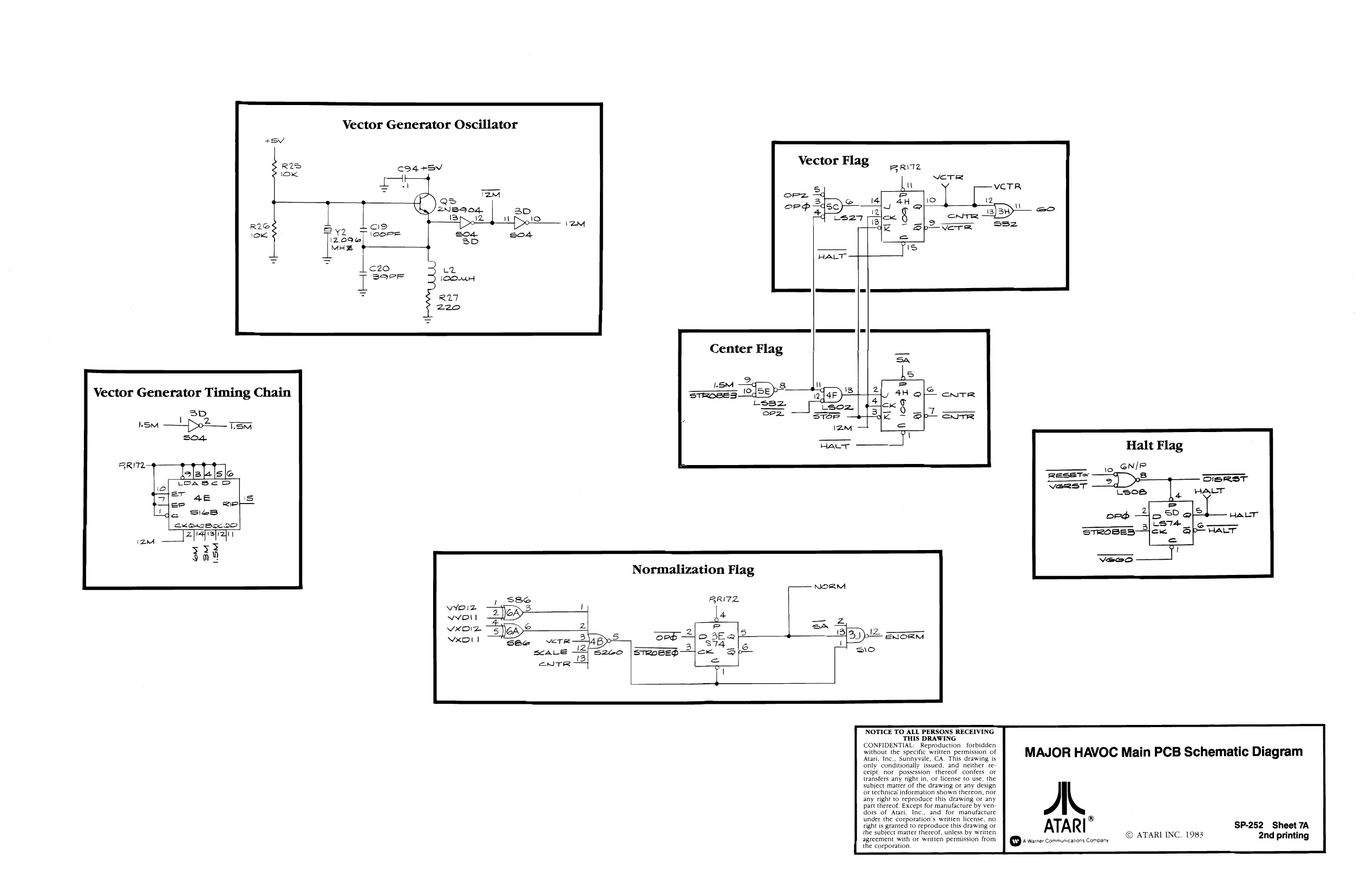
This page is a drawing, shown as the original scan.
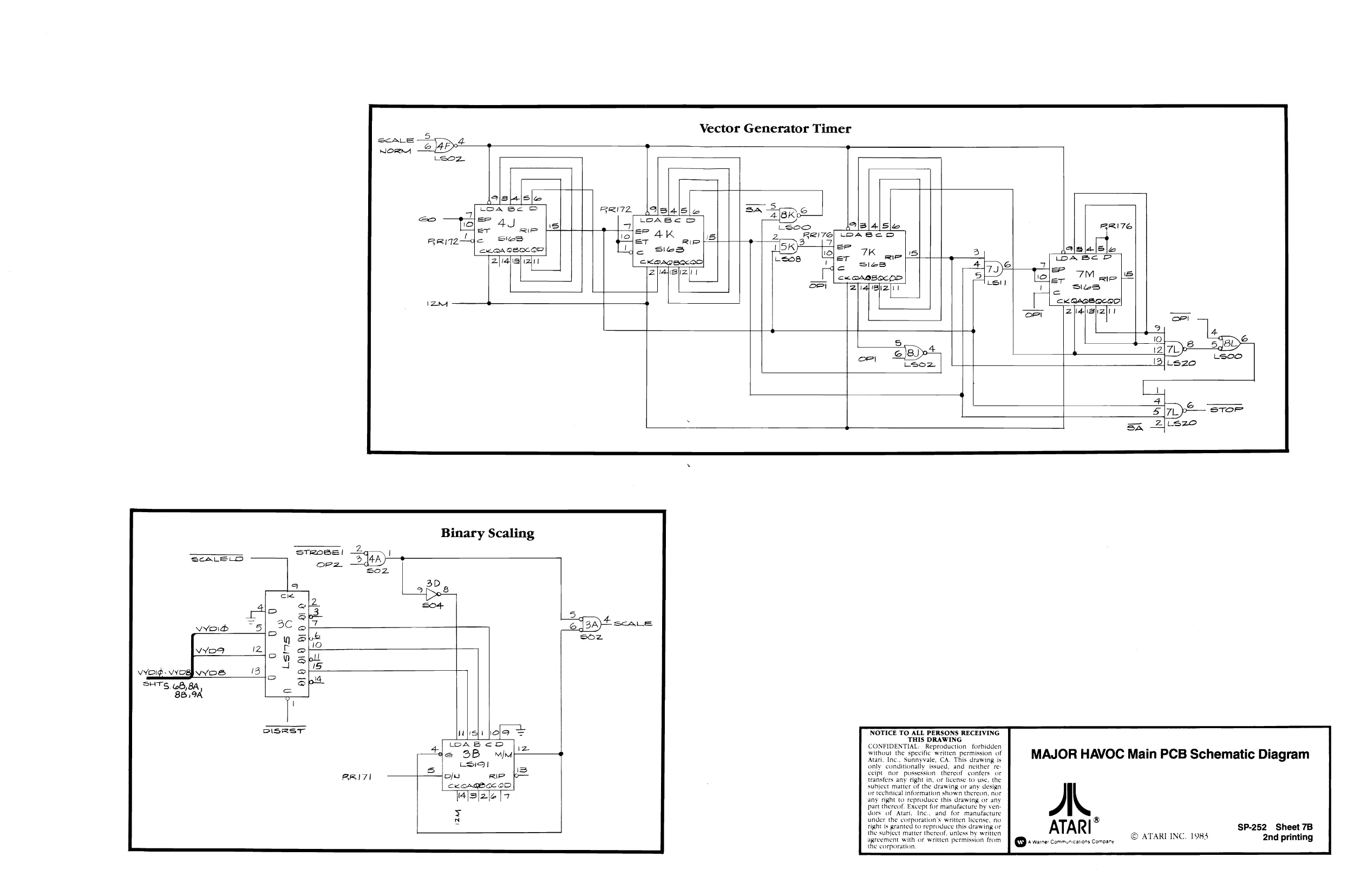
This page is a drawing, shown as the original scan.
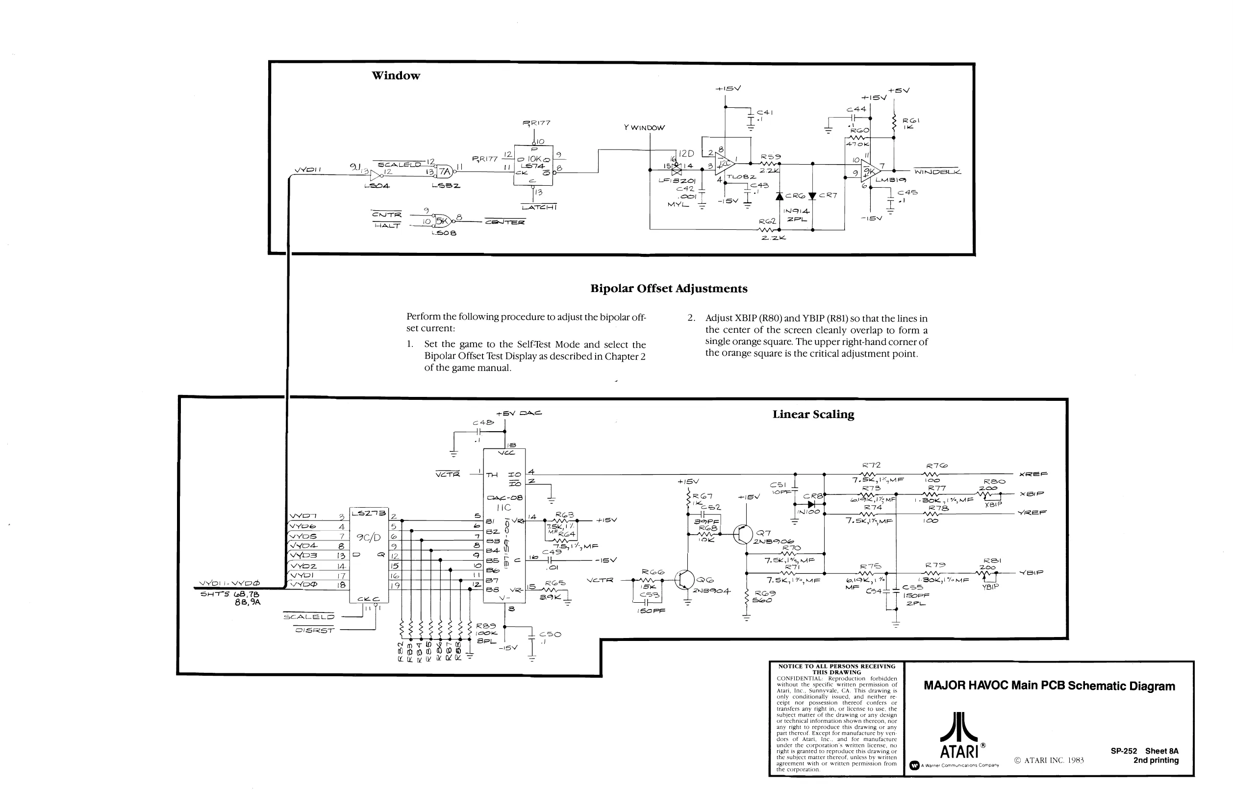
8, VYDII-VYDD
SHTS B,7BR SA RR?
215 10ko|2 Cert af 7Ap ut jhe oe Y window
9/2 wrosoe Luaiey J ds zo
-15v
Bipolar Offset Adjustments
Perform the following procedure to adjust the bipolar offset current:
- Set the game to the Self-Test Mode and select the Bipolar Offset Test Display as described in Chapter 2 of the game manual. Adjust XBIP (R80) and YBIP (R81) so that the lines in the center of the screen cleanly overlap to form a single orange square. The upper right-hand corner of the orange square is the critical adjustment point.
Linear Scaling
RTS
2 Sle, pet paki _— tsv 2 So eo + ry ala T . a
15 +_2 ne
otc Ss REO R77 zoo
TAOS re COT 278 ie xe
vRer
FS 1% Me RGD com (S0PF 505 2eL
NOTICE TO ALL PERSONS RECEIVING THIS DRAWING CONFIDENTIAL: Reproduction forbidden without the specific ‘written permission of Atari, Inc., Sunnyvale, CA. This drawing is only’ conditionally issued, and- neither re Ceipt nor possession thereof confers or transfers any right in, or license 10 use, the subject matter of the drawing or any design Or technical information showa thereon, nor any right to reproduce this drawing or any
part thereof. Except for manufacture by ven right is granted to reproduce this drawing or
dors of Atari, Inc., and for manufacture tnder the corporation's written license, 80
the subject matter thereof, ualess by written, agreement with or written permission from the corporation. A.
ATARI”
ATARI INC. 1983
MAJOR HAVOC Main PCB Schematic Diagram
SP-252 Sheet 8A 2nd printing
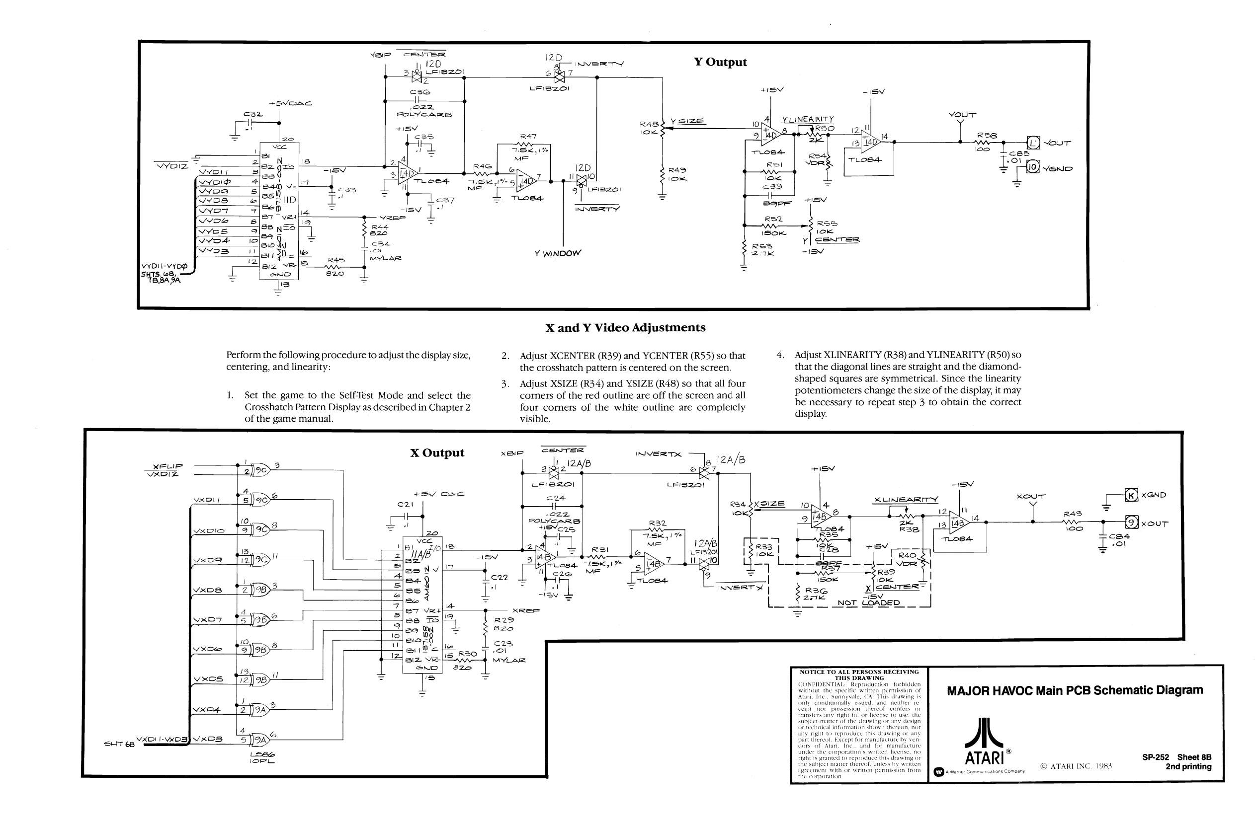
SHT 6B
Y Output
VXDUL-VXD EJ VXOS Perform the following procedure to adjust the display size, centering, and linearity:
Set the game to the SelfTest Mode and select the Crosshatch Pattern Display as described in Chapter 2 of the game manual.
X Output
a is G ysize o See |
Y WINDOW
X and Y Video Adjustments
Adjust XCENTER (R39) and YCENTER (R55) so that the crosshatch pattern is centered on the screen.
Adjust XSIZE (R34) and YSIZE (R48) so that all four corners of the red outline are off the screen and all four corners of the white outline are completely visible.
4B BI Rosa TSK,17 c2e MF 0 | oS fn} fw fr |
o
iy YLINEARITY
4.
INNERT > | Le Adjust XLINEARITY (R38) and YLINEARITY (R50) so that the diagonal lines are straight and the diamondshaped squares are symmetrical. Since the linearity potentiometers change the size of the display, it may be necessary to repeat step 3 to obtain the correct display.
NOTICE TO ALL PERSONS RECEIVING THIS DRAWING CONFIDENTIAL: Reproduction forbidden without the specific written permission of Atari, Inc., Sunnyvale, CA. This drawing is only’ conditionally issued, and neither re Geipt_nor possession thereof conkers oF transfers any right in, oF heense to use, the
subject matier of the drawing or any design part thereol, Except for manufacture by ven right is granted to reproduce this drawing or
Gr technical information shown thereon, Ot any right to reproduce this drawing or any
dfs of Atari, Ine, and for manufactuce Under the corporation's written license, 0
ascent wih of writen periion fon Yaar conmncatarsConoany © ATARI INC. 1984
MAJOR HAVOC Main PCB Schematic Diagram
SP-252 Sheet 8B 2nd printing
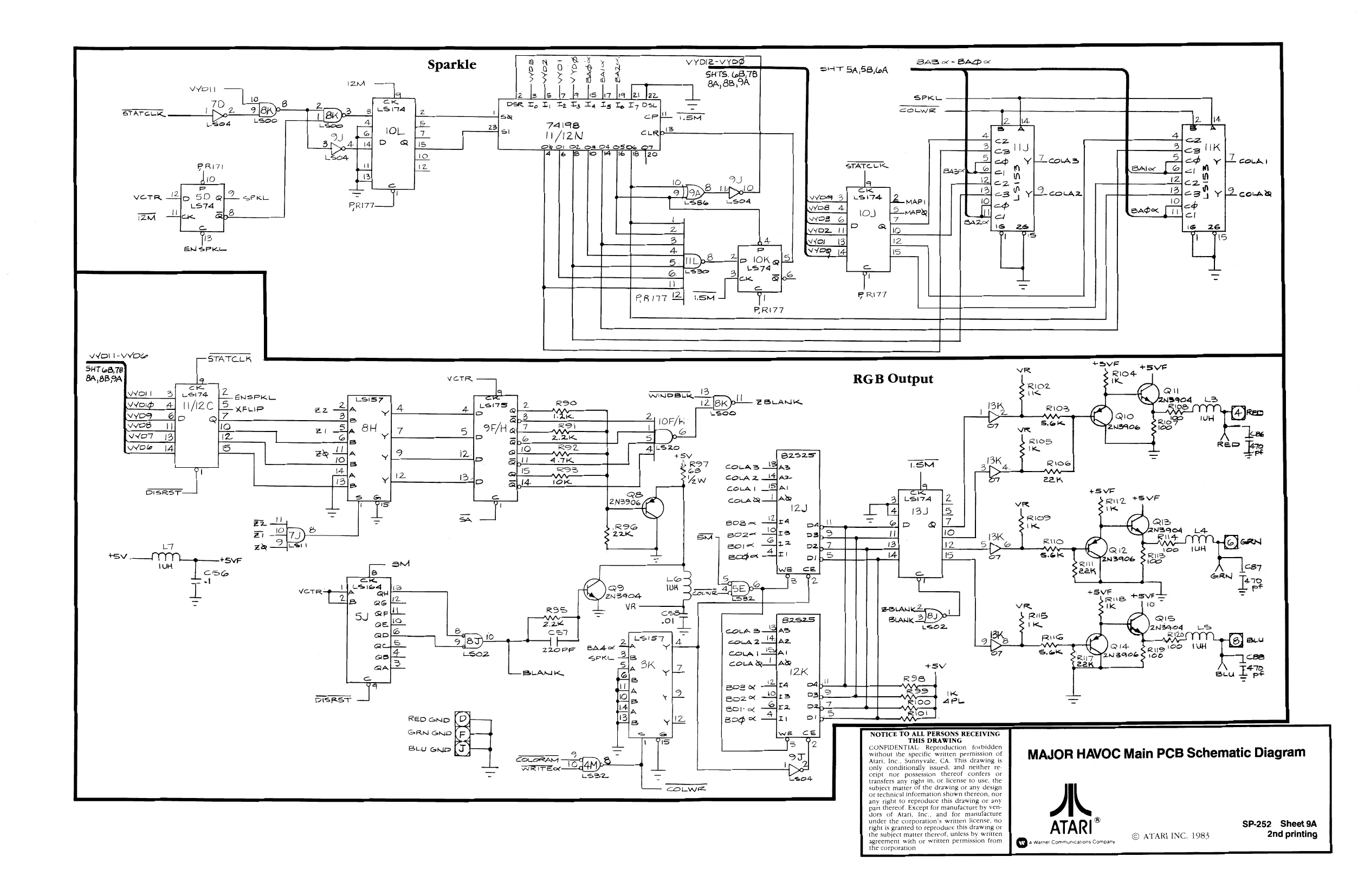
This page is a drawing, shown as the original scan.
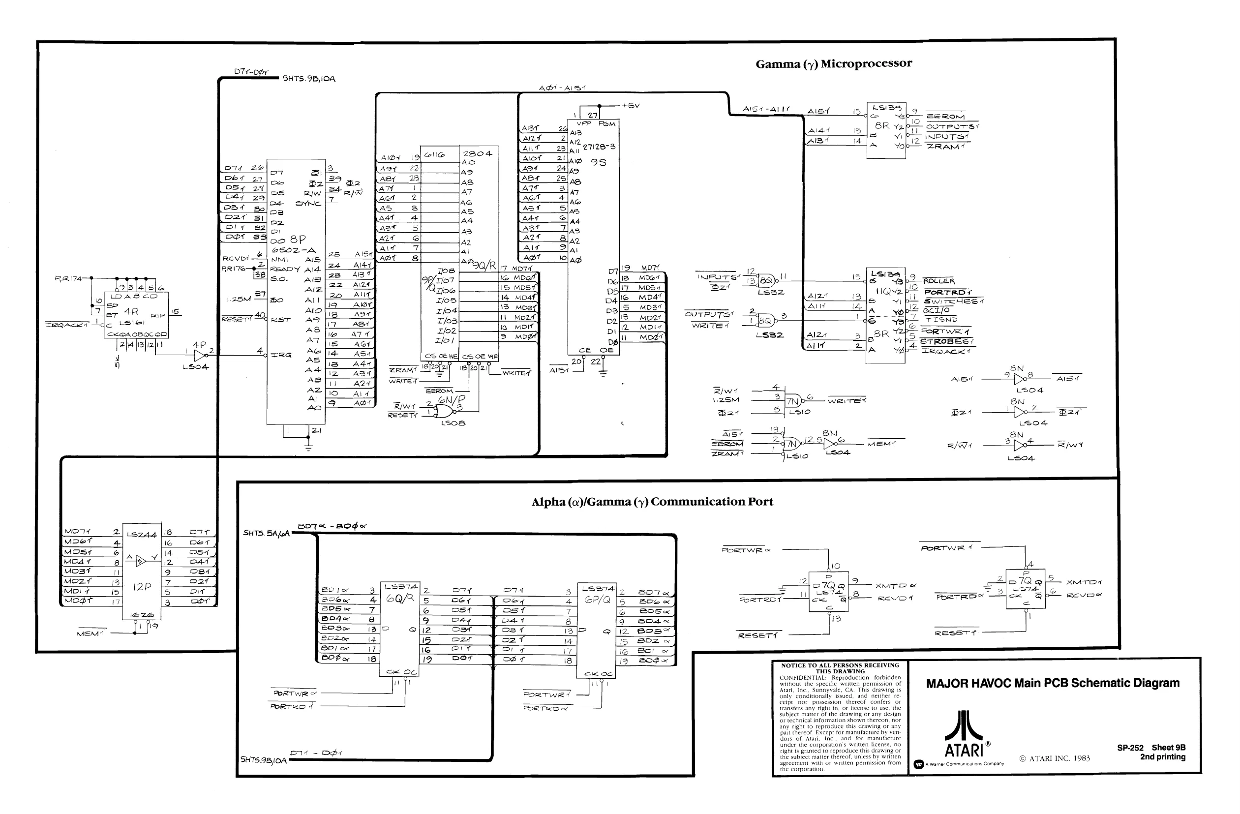
This page is a drawing, shown as the original scan.
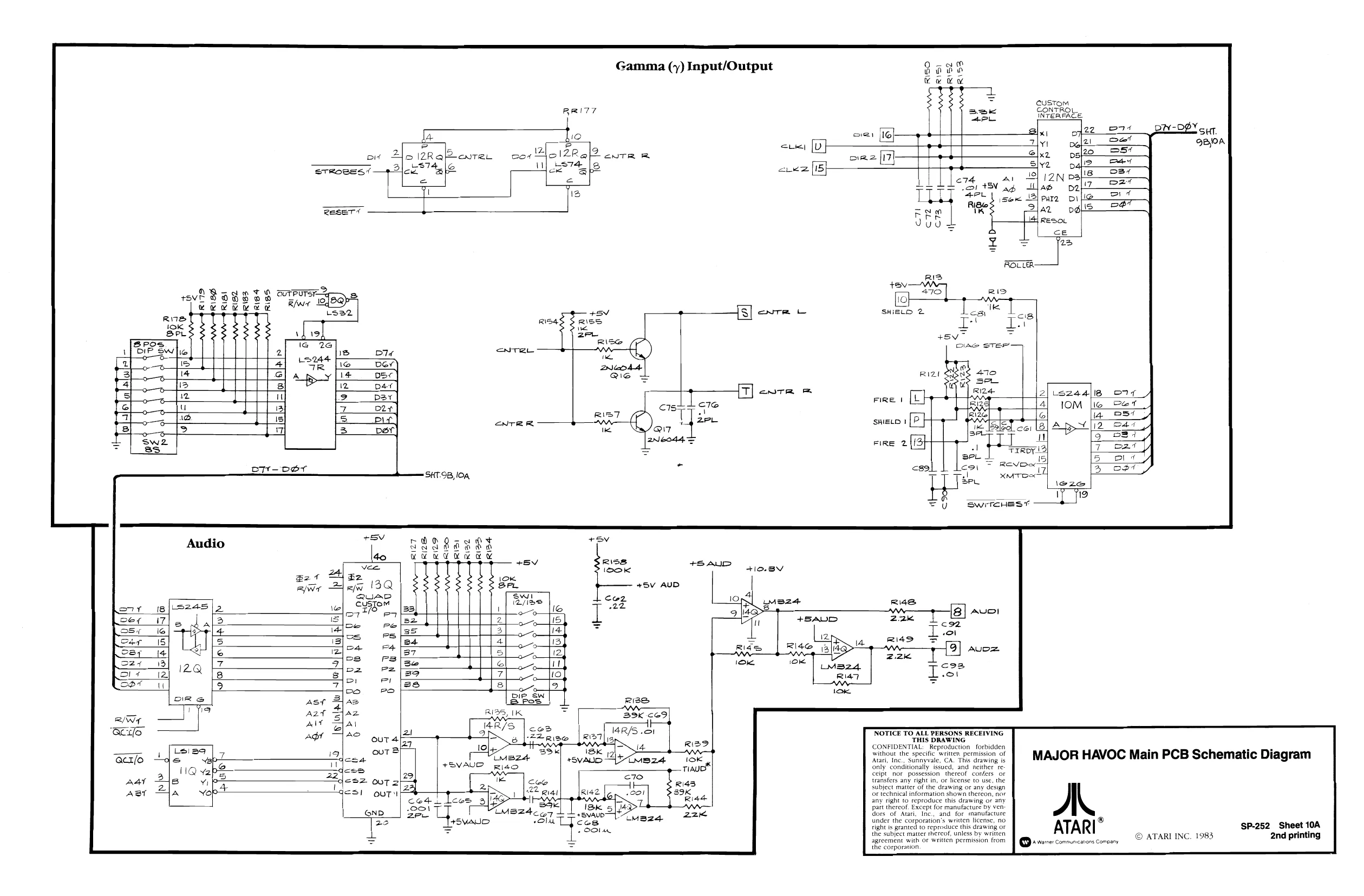
This page is a drawing, shown as the original scan.