Super Sprint SP-290 1st Printing
Super Sprint (rev 4) (Atari Games, 1986) · Schematic Package · 33 pages · 79 sections · original scan
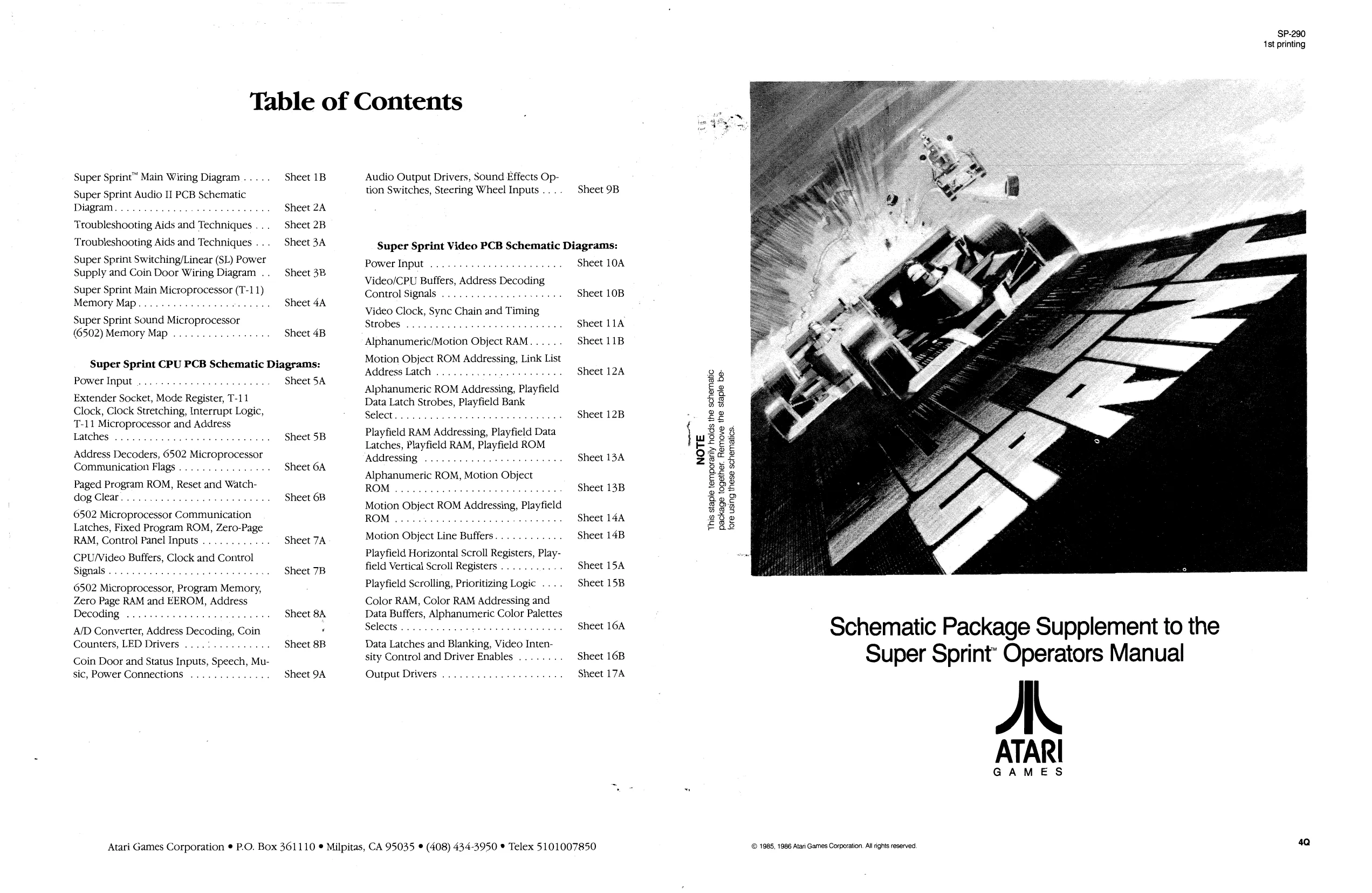
Table of Contents
Super Sprint™ Main Wiring Diagram ..... Sheet 1B Super Sprint Audio II PCB Schematic Diagram. .... eet eee Sheet 2A Troubleshooting Aids and Techniques Sheet 2B Troubleshooting Aids and Techniques... Sheet 3A. Super Sprint Switching/Linear (SL) Power Supply and Coin Door Wiring Diagram .. Sheet 3B Super Sprint Main Microprocessor (T-11) Memory Map.............0.0 0200005 Sheet 4A Super Sprint Sound Microprocessor (6502) Memory Map ............-- Sheet 4B
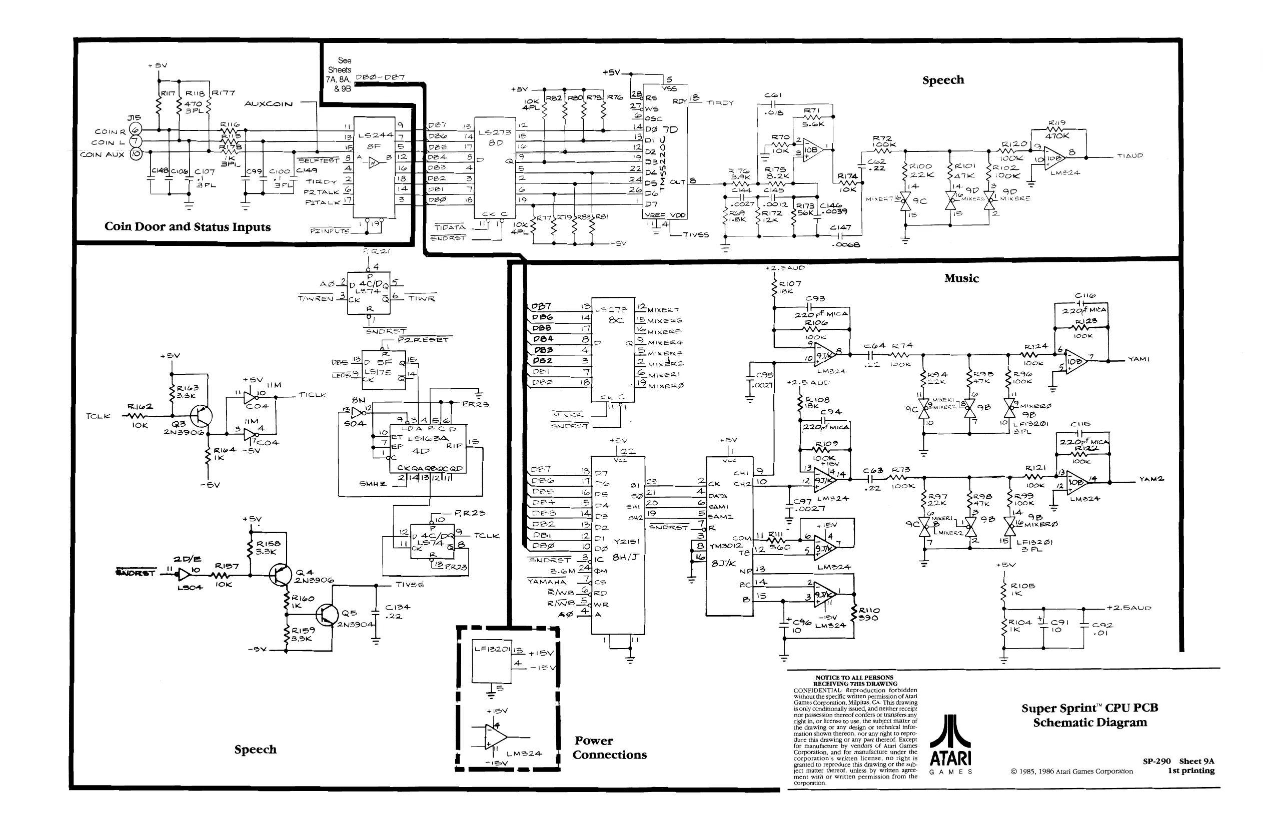
Super Sprint CPU PCB Schematic Diagrams: Power Input ......-.........- Sheet 5A Extender Socket, Mode Register, T-11 Clock, Clock Stretching, Interrupt Logic, T-11 iaiataaeaiiil and Address Latches 6.00.0... cece eee eee eee Sheet 5B Address Decoders, 6502 12 Microprocessor Communication Flags............ Sheet 6A Paged Program ROM, Reset and Watchdog Clear... 20.0... 2c eee : Sheet 6B 6502 Microprocessor Communication Latches, Fixed Program ROM, ceo RAM, Control Panel Inputs ...... .. Sheet 7A CPU/Video Buffers, Clock and Control Signals . . fete ns era ee eae Sheet 7B 6502 Microprocessor, Program Memory, Zero Page RAM and EEROM, Address Decoding ...........0...0005 . Sheet 8A A/D Converter, Address Decoding, Coin * Counters, LED Drivers ....:...... -. Sheet 8B Coin Door and Status Inputs, Speech, Music, Power Connections ar Sheet 9A Audio Output Drivers, Sound Effects Option Switches, Steering Wheel Inputs . . . Sheet 9B
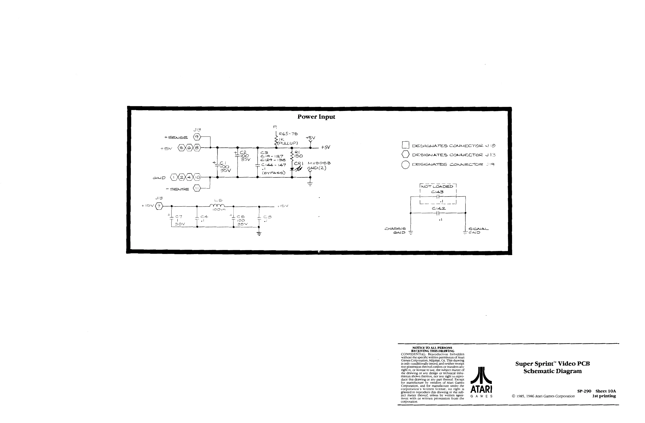
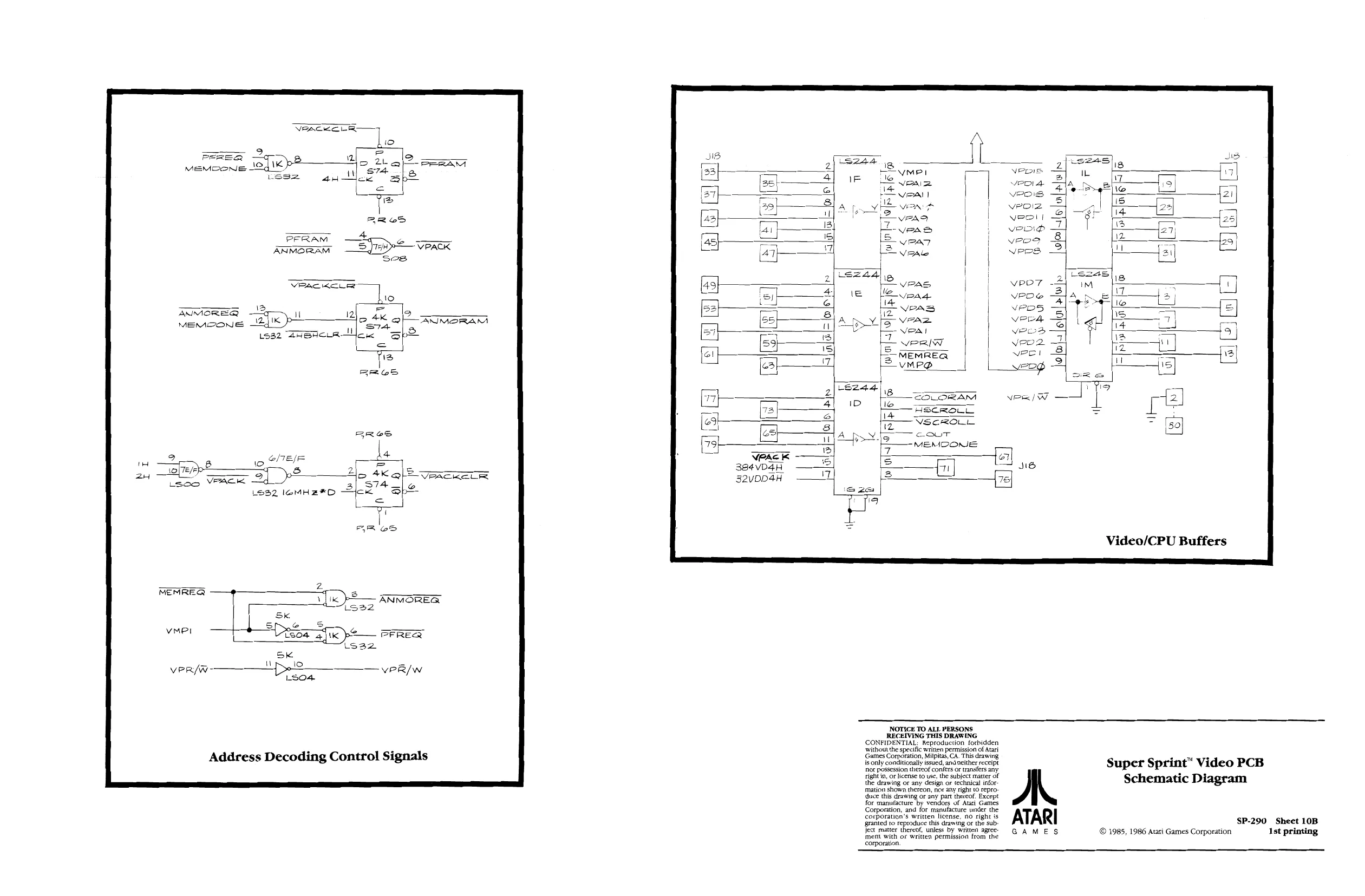
Super Sprint Video PCB Schematic Diagrams: Power Input ........ Sheet 10A Video/CPU Buffers, Address Deco Control Signals ...........0 006 e eee Sheet 10B Video Clock, Sync Chain and Timing Strobes cece eee see Sheet 11A Alphanumeric/Motion Object RAM...... Sheet 11B Motion Object ROM Addressing, Link List Address Latch ........... Sheet 12A Alphanumeric ROM Addressing, Playfield Data Latch Strobes, Playfield Bank Select......... . Sheet 12B Playfield RAM Addressing, Playfield Data Latches, Playfield RAM, Playfield ROM Addressing ............520.05 . Sheet 13A Aippanumeric ROM, Motion Object ROM 2.0... 0c cece eee ee Sheet 13B Motion Object ROM Addressing, Playfield ROM 2... eee tee Sheet 14A Motion Object Line Buffers......... .. Sheet 14B Playfield Horizontal Scroll Registers, Playfield Vertical Scroll Registers . . . . . Sheet 15A Playfield Scrolling, Prioritizing Logic .. . Sheet 15B Color RAM, Color RAM Addressing and Data Buffers, Alphanumeric Color Palettes Selects... 2.0.00. 00 ee eee eee Sheet 16A
Data Latches and Blanking, Video Intensity Control and Driver Enables . Sheet 16B Output Drivers ............ 00200 Sheet 17A
Atari Games Corporation ¢ P.O. Box 361110 © Milpitas, CA 95035 © (408) 434-3950 ® Telex 5101007850
fore using these schematics. ‘SP-290 1st printing
Schematic Package Supplement to the Super Sprint’ Operators Manual
AN ATARI GAMES
© 1985, 1986 Atari Games Corporation. All rights reserved. 4a
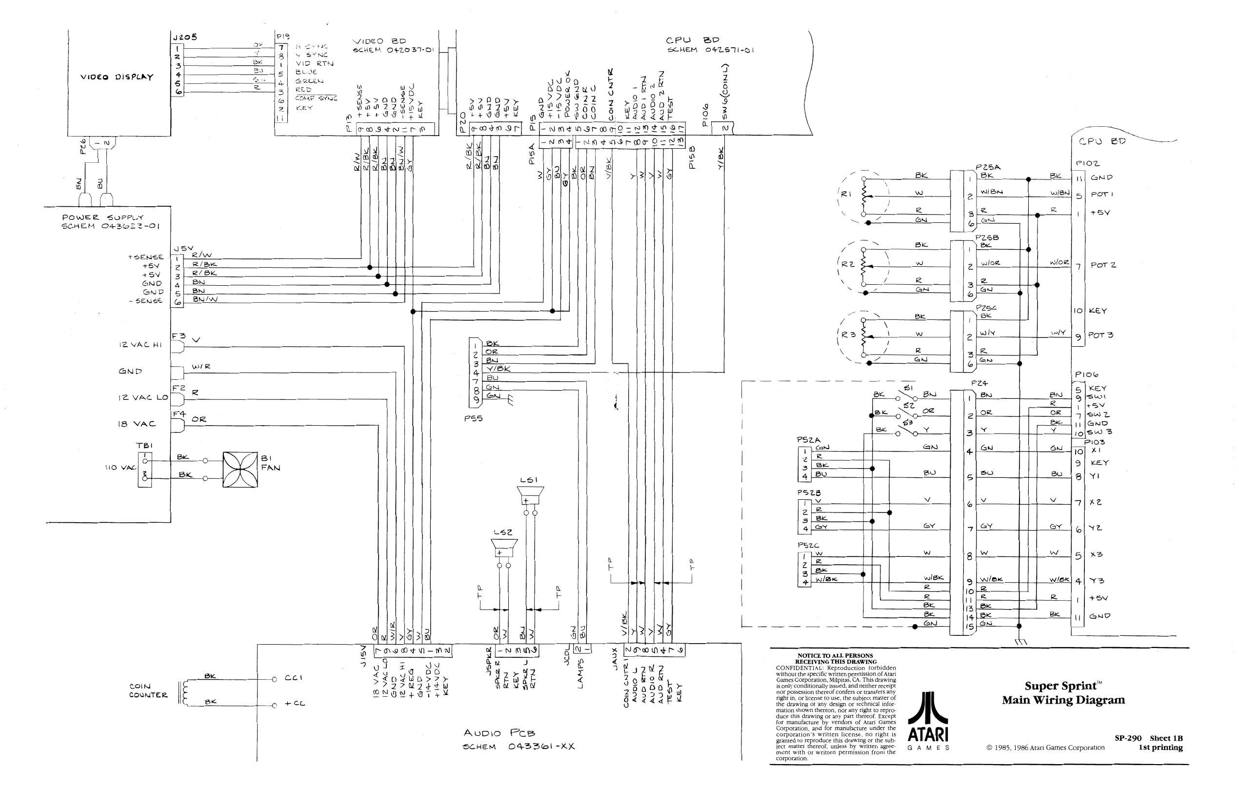
This page is a drawing, shown as the original scan.
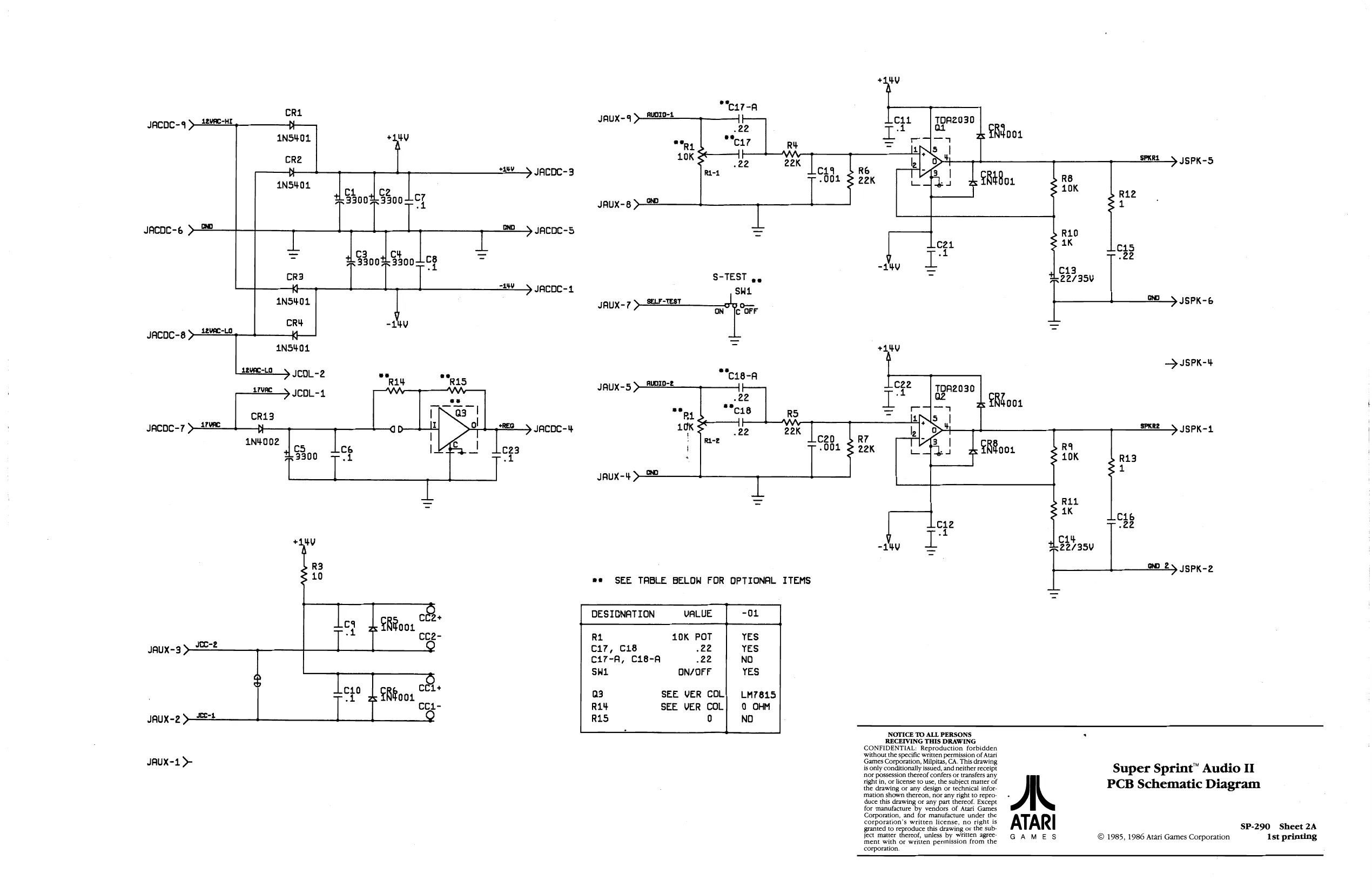
This page is a drawing, shown as the original scan.
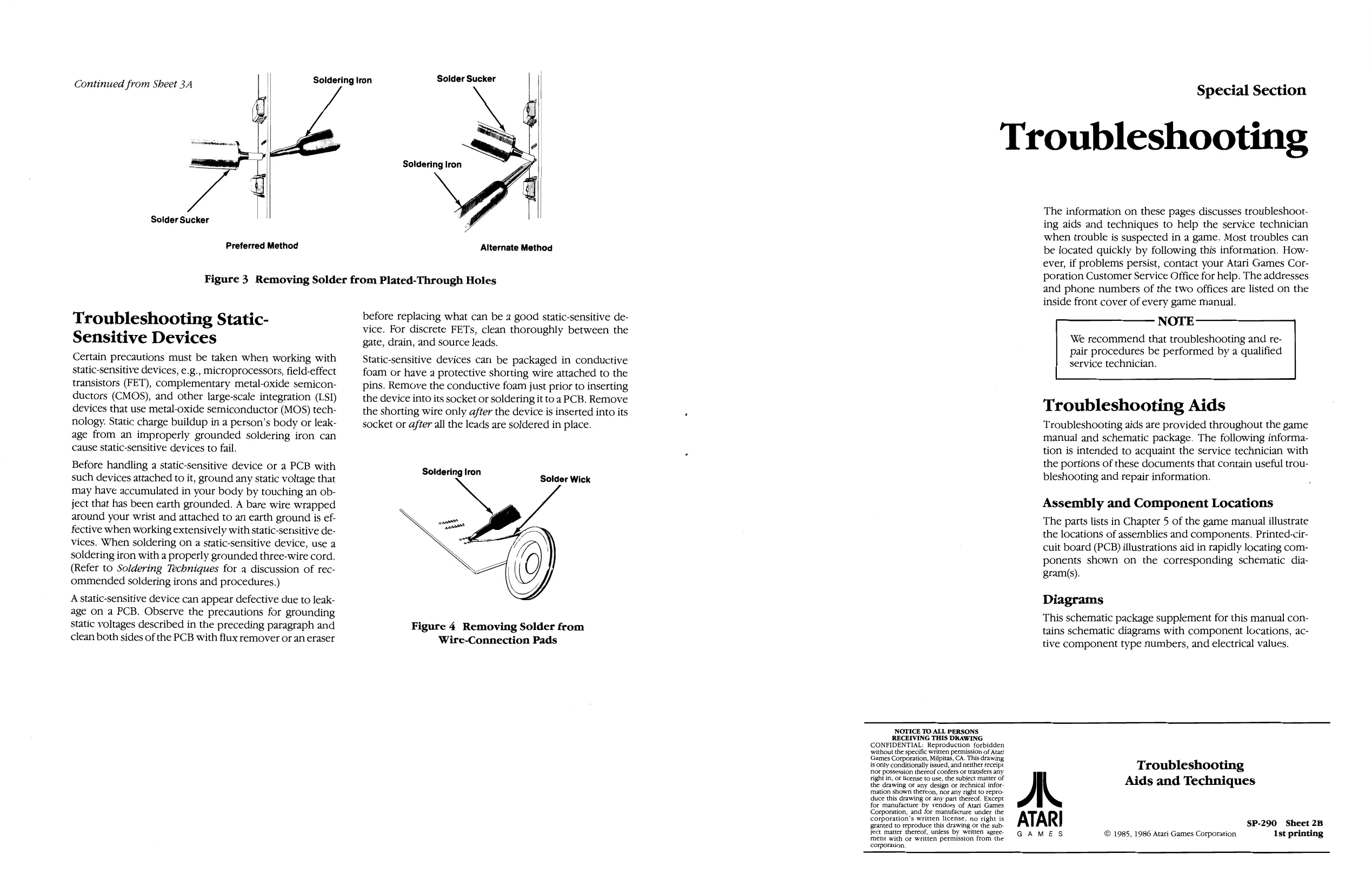
Continued from Sheet 3A
Solder Sucker
Preferred Method Soldering Iron Solder Sucker
Soldering Iron
Alternate Method
Figure 3 Removing Solder from Plated-Through Holes
Troubleshooting Static-
Sensitive Devices
Certain precautions must be taken when working with static-sensitive devices, e.g., microprocessors, field-effect transistors (FET), complementary metal-oxide semiconductors (CMOS), and other large-scale integration (LSI) devices that use metal-oxide semiconductor (MOS) technology. Static charge buildup in a person’s body or leakage from an improperly grounded soldering iron can Cause static-sensitive devices to fail.
Before handling a static-sensitive device or a PCB with
such devices attached to it, ground any static voltage that may have accumulated in your body by touching an object that has been earth grounded. A bare wire wrapped around your wrist and attached to an earth ground is effective when working extensively with static-sensitive devices, When soldering on a static-sensitive device, use a soldering iron with a properly grounded three-wire cord. (Refer to Soldering Techniques for a discussion of recommended soldering irons and procedures.) A static-sensitive device can appear defective due to leakage on a PCB. Observe the precautions for grounding Static voltages described in the preceding paragraph and clean both sides of the PCB with flux remover or an eraser before replacing what can be a good static-sensitive device. For discrete FETs, clean thoroughly between the gate, drain, and source leads. Static-sensitive devices can be packaged in conductive foam or have a protective shorting wire attached to the pins. Remove the conductive foam just prior to inserting the device into its socket or soldering it toa PCB. Remove the shorting wire only after the device is inserted into its socket or after all the leads are soldered in place.
Soldering Iron Solder Wick
Figure 4 Removing Solder from Wire-Connection Pads
Special Section
Troubleshooting
NOTICE TO ALL PERSONS: RECEIVING THIS DRAWING CONFIDENTIAL: Reproduction forbidden ‘without the specific written permission of Atari Games Corporation, Milpitas, CA. This drawing. is only conditionally issued, and neither receipt Nor possession thereof confers or transfers any The information on these pages discusses troubleshooting aids and techniques to help the service technician when trouble is suspected in a game. Most troubles can be iocated quickly by following this information. However, if problems persist, contact your Atari Games Corporation Customer Service Office for help. The addresses and phone numbers of the two offices are listed on the inside front cover of every game manual.
Troubleshooting Aids
Troubleshooting aids are provided throughout the game manual and schematic package. The following information is intended to acquaint the service technician with the portions of these documents that contain useful troubleshooting and repair information.
Assembly and Component Locations The parts lists in Chapter 5 of the game manual illustrate the locations of assemblies and components, Printed-circuit board (PCB) illustrations aid in rapidly locating components shown on the corresponding schematic diagram(s).
Diagrams This schematic package supplement for this manual contains schematic diagrams with component locations, active component type numbers, and electrical values.
right in, of license to use, the subject matter of tT the drawing oF any. design or technical infor Aids and Techniques de Hil Swng tr pad ieee aoe foc manufacture by veridorg of Ate Games Corporation and for manacue det the ranted to teproduce this drawing Or the sub SP-290 Sheet 2B Ject matter thereof, unless by written agree «GA ME S © 1985, 1986 Atari Games Corporation 1st printiny ment with or written permission fromthe © a “po Printing corporation
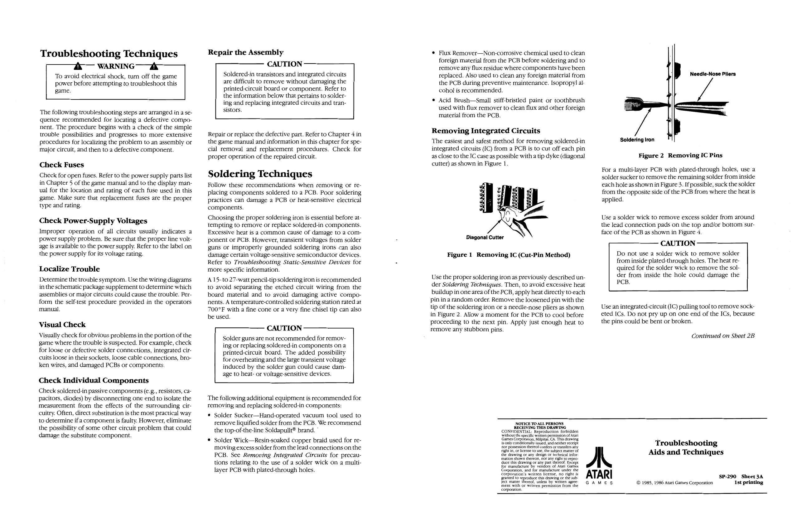
Troubleshooting Techniques
To avoid electrical shock, turn off the game power before attempting to troubleshoot this game.
The following troubleshooting steps are arranged in a sequence recommended for locating a defective component. The procedure begins with a check of the simple trouble possibilities and progresses to more extensive procedures for localizing the problem to an assembly or major circuit, and then to a defective component.
Check Fuses Check for open fuses. Refer to the power supply parts list in Chapter 5 of the game manual and to the display manual for the location and rating of each fuse used in this game. Make sure that replacement fuses are the proper type and rating.
Check Power-Supply Voltages
Improper operation of all circuits usually indicates a power supply problem. Be sure that the proper line voltage is available to the power supply. Refer to the label on the power supply for its voltage rating.
Localize Trouble Determine the trouble symptom. Use the wiring diagrams in the schematic package supplement to determine which assemblies or major circuits could cause the trouble. Perform the self-test procedure provided in the operators manual.
Visual Check Visually check for obvious problems in the portion of the game where the trouble is suspected. For example, check for loose or defective solder connections, integrated circuits loose in their sockets, loose cable connections, broken wires, and damaged PCBs or components
Check Individual Components
Check soldered-in passive components (e.g., resistors, capacitors, diodes) by disconnecting one end to isolate the measurement from the effects of the surrounding circuitry. Often, direct substitution is the most practical way to determine ifa component is faulty. However, eliminate the possibility of some other circuit problem that could damage the substitute component. Repair the Assembly
Repair or replace the defective part. Refer to Chapter 4 in the game manual and information in this chapter for special removal and replacement procedures. Check for proper operation of the repaired circuit.
Soldering Techniques
Follow these recommendations when removing or replacing components soldered to a PCB. Poor soldering practices can damage a PCB or heat-sensitive electrical components. Choosing the proper soldering iron is essential before attempting to remove or replace soldered-in components. Excessive heat is a common cause of damage to a component or PCB. However, transient voltages from solder guns or improperly grounded soldering irons can also damage certain voltage-sensitive semiconductor devices. Refer to Troubleshooting Static-Sensitive Devices for more specific information. A15-to 27-watt pencil-tip soldering iron is recommended to avoid separating the etched circuit wiring from the board material and to avoid damaging active components. A temperature-controlled soldering station rated at 700°F with a fine cone or a very fine chisel tip can also be used.
The following additional equipment is recommended for removing and replacing soldered-in components:
- Solder Sucker—Hand-operated vacuum tool used to remove liquified solder from the PCB. We recommend. the top-of-the-line Soldapullt® brand. Solder Wick—Resin-soaked copper braid used for removing excess solder from the lead connections on the PCB. See Removing Integrated Circuits for precautions relating to the use of a solder wick on a multilayer PCB with plated-through holes.
- Flux Remover—Non-corrosive chemical used to clean foreign material from the PCB before soldering and to remove any flux residue where components have been replaced. Also used to clean any foreign material from the PCB during preventive maintenance. Isopropyl alcohol is recommended. e Acid Brush—Small stiff-bristled paint or toothbrush used with flux remover to clean flux and other foreign material from the PCB.
Removing Integrated Circuits
The easiest and safest method for removing soldered-in integrated circuits (IC) from a PCB is to cut off each pin as close to the IC case as possible with a tip dyke (diagonal cutter) as shown in Figure 1.
Diagonal Cutter
Figure 1 Removing IC (Cut-Pin Method)
Use the proper soldering iron as previously described under Soldering Techniques. Then, to avoid excessive heat buildup in one area of the PCB, apply heat directly to each pin ina random order. Remove the loosened pin with the tip of the soldering iron or a needle-nose pliers as shown. in Figure 2. Allow a moment for the PCB to cool before proceeding to the next pin. Apply just enough heat to remoye any stubborn pins.
NOTICE TO ALL PERSONS
RECEIVING THIS DRAWING CONFIDENTIAL: Reproduction forbidden ‘without the specific written permission of Atari Games Corporation, Milpitas, CA. This drawing. is only conditionally issued, and neither receipt nor possession thereof confers or transfers any right in, oF license to use, the subject matter of the drawing or any design or technical infor mation shown thereon, nor any right to repro duce this drawing or any part thereof. Except for manufacture by vendors of Atari Games Corporation, and for manufacture under the corporation's written license, no right is granted to reproduce this drawing or the subject matter thereof, unless by written agree ment with or written permission from the corporation. Needle-Nose Pliers
Soldering Iron
Figure 2 Removing IC Pins
For a multi-layer PCB with plated-through holes, use a solder sucker to remove the remaining solder from inside each hole as shown in Figure 3. If possible, suck the solder from the opposite side of the PCB from where the heat is applied.
Use a solder wick to remove excess solder from around the lead connection pads on the top and/or bottom surface of the PCB as shown in Figure 4.
Use an integrated-circuit (IC) pulling tooi to remove socketed ICs. Do not pry up on one end of the ICs, because the pins could be bent or broken.
Continued on Sheet 2B
Troubleshooting NM Aids and Techniques ATARI SP-290 Sheet 3A GAMES © 1985, 1986 Atari Games Corporation 1st printing
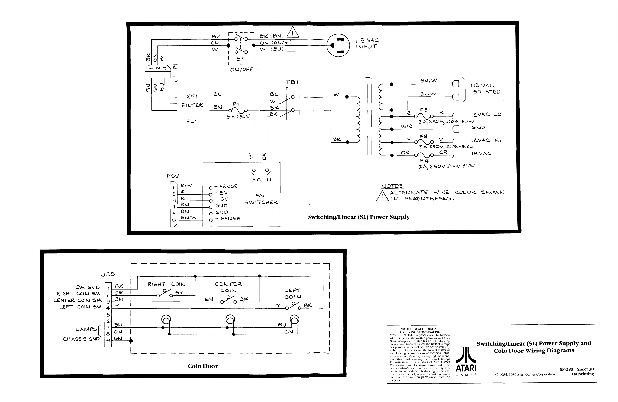
This page is a drawing, shown as the original scan.
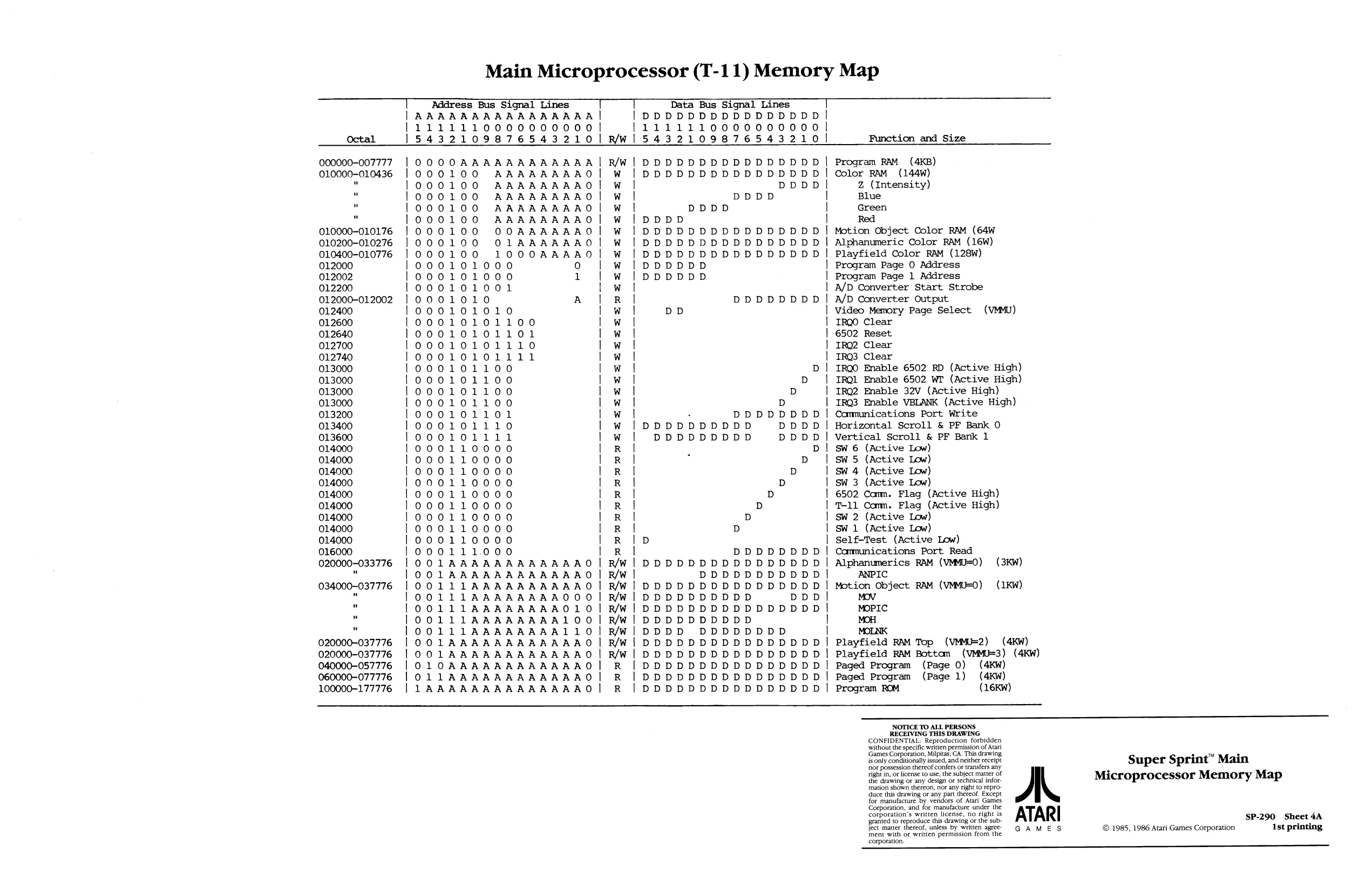
This page is a drawing, shown as the original scan.
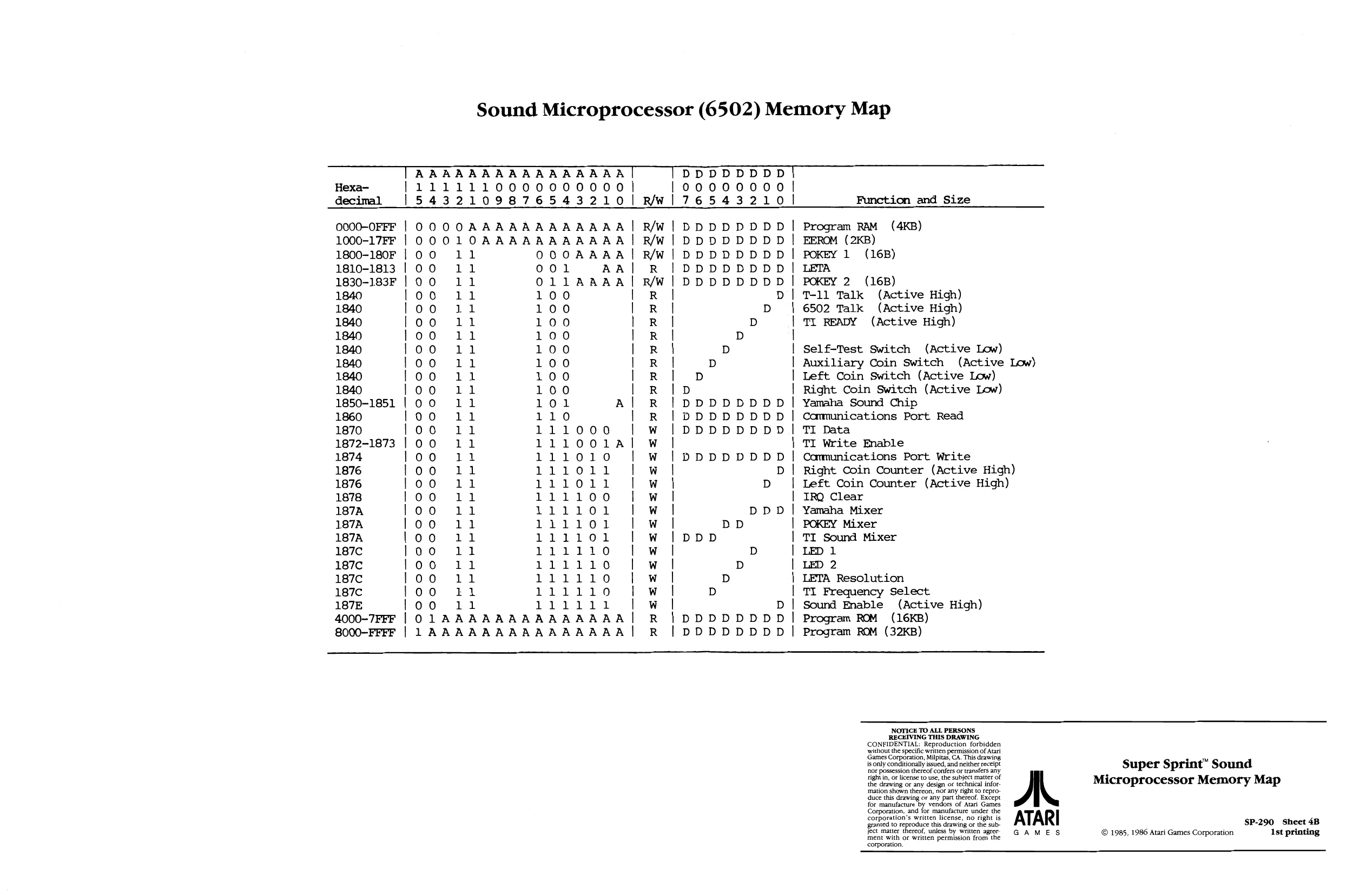
This page is a drawing, shown as the original scan.
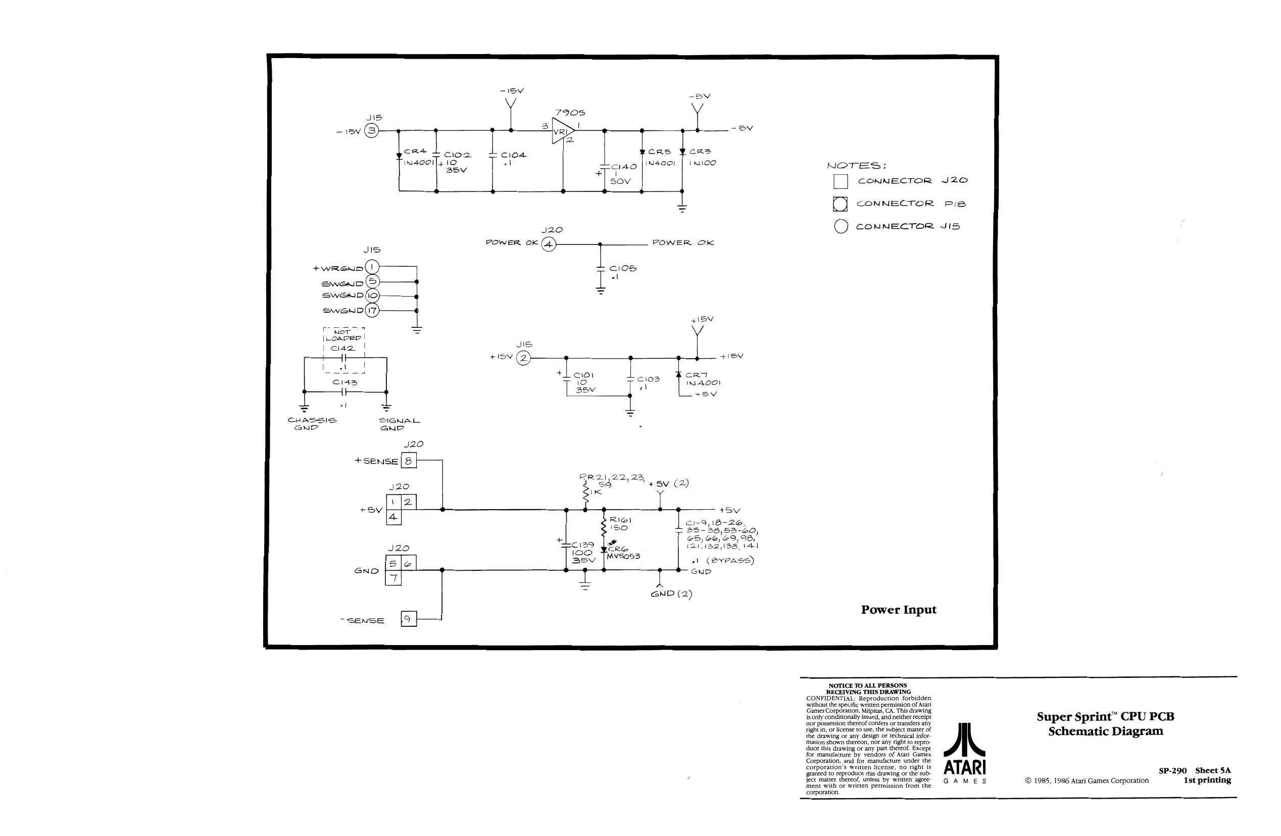
This page is a drawing, shown as the original scan.
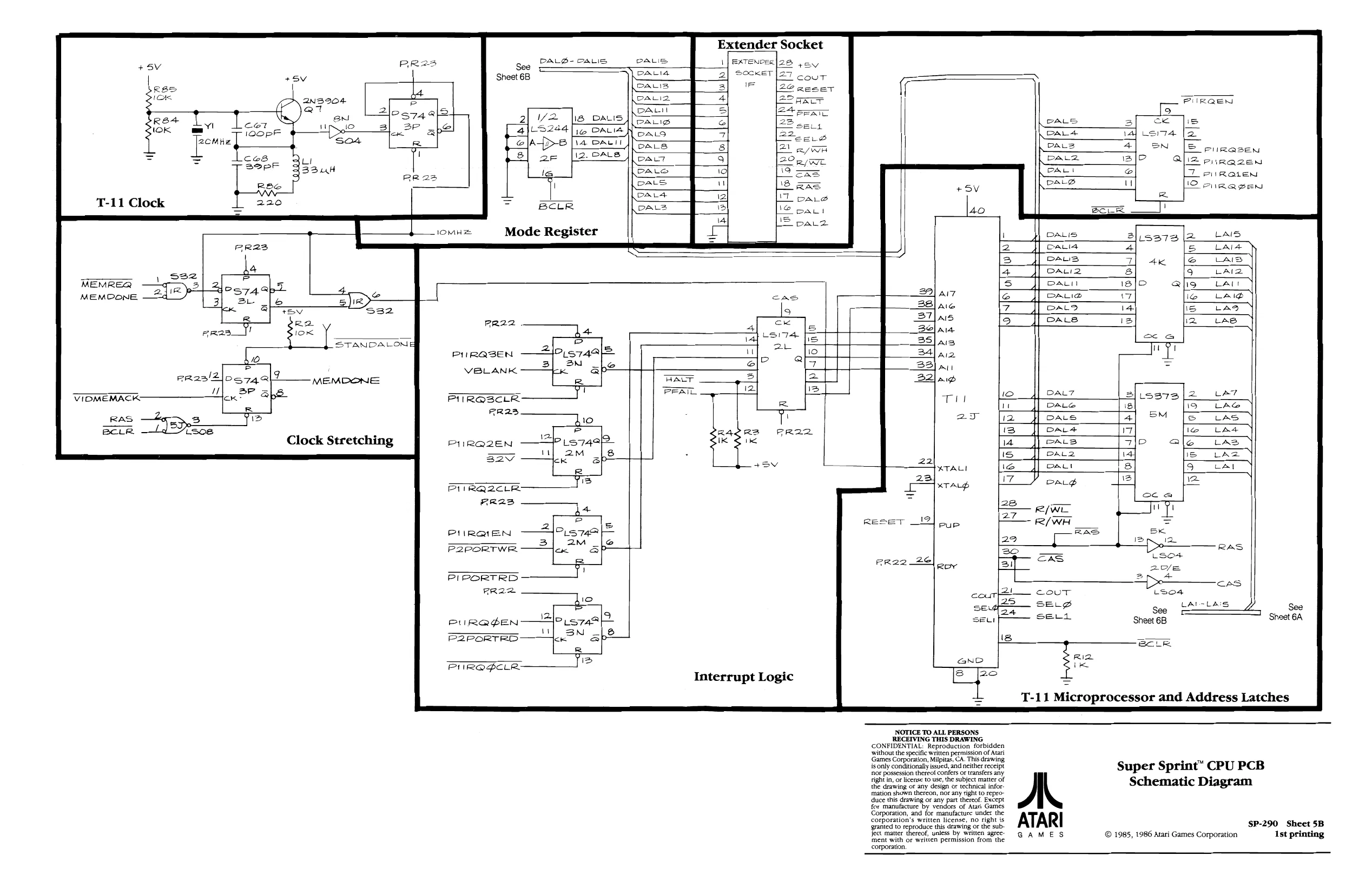
This page is a drawing, shown as the original scan.
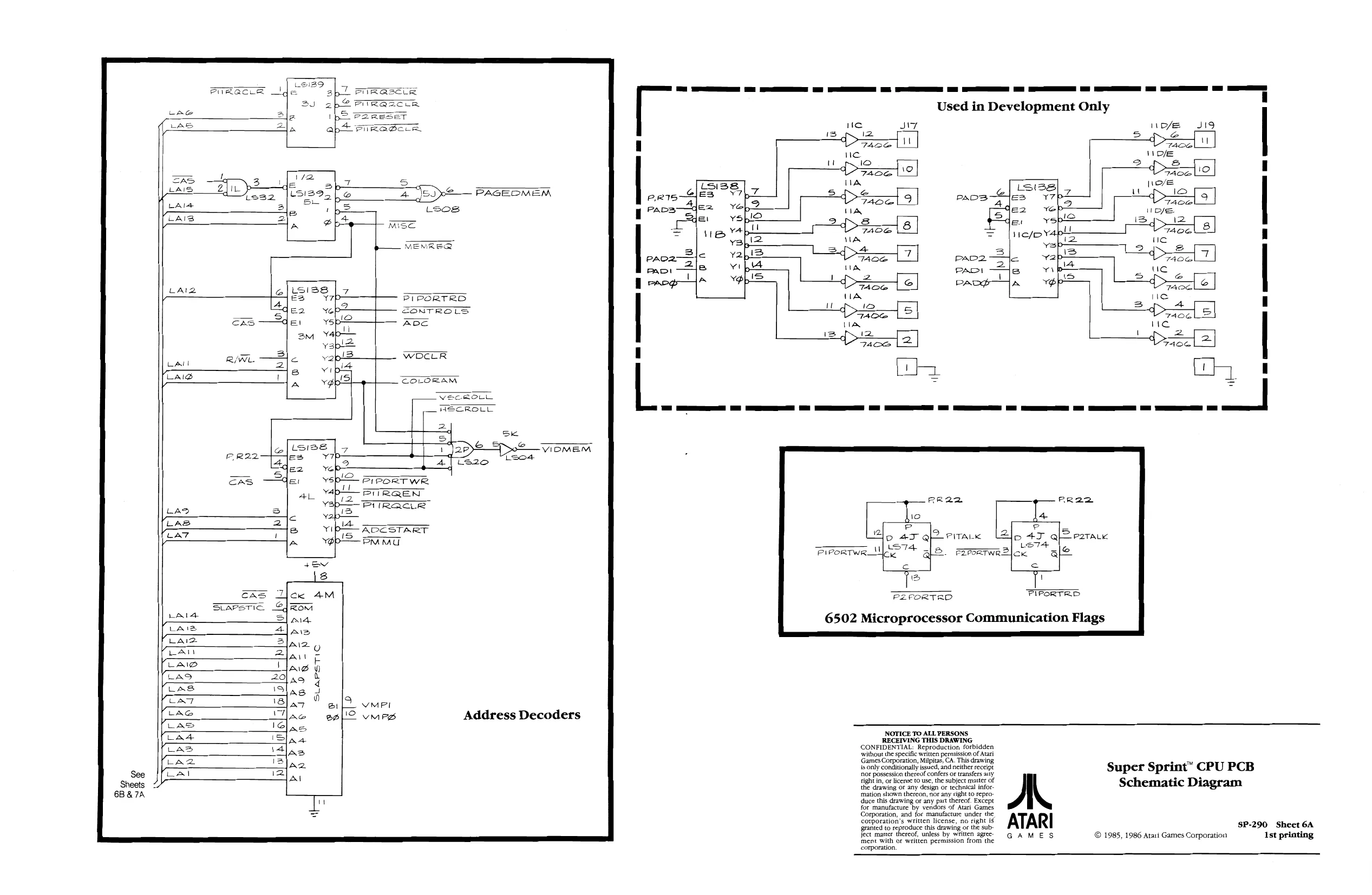
TRAQBELR b2 PTRASeLR PaReSseT
be 5 a EDS — PAGEDMEM Lsos
MSE
}__ WEWREQ
PIPORTRO EONTROLS
PIPORT WR SU RQEN 2 SRA 1S RAC
4 AGZSTART
1s
CAS SAPs LaLa
LA
LAIz LAI LAID es MMU
Address Decoders PADZ
PADI
Used in Development Only
np/e JI9 S A Doel! Oe 2 s&s peal oe [SI5El 7 ra enya)
| PADS | r=. | v7 | 3 | { | —voaes | 3g |
a {E2 "EPS es er ysple is 12. = tL = |lic/oY4p> yap S
| PaAD2Z | Feast | v2 | = |
| PADI | 3B | vps | |
| PAcd | a | yp |
IP
SP ITALK e
PIPORTWR. [&. eapoRTWwRe Ion ale p47 al2rztak Ler i
S ] 1 FIFORTRD
6502 Microprocessor Communication Flags
NOTICE TO ALL PERSONS,
RECEIVING THIS DRAWING. CONFIDENTIAL: Reproduction forbidden without the specific written permission of Atari ‘Games Corporation, Milpitas, CA. This drawing 's only conditionally issued, and neither receipt ‘nor possession thereof confers or transfers any right in, or license t0 use, the subject matter of the drawing or any design or technical infor- ‘mation shown thereon, nor any right to repro, duce this drawing or any part thereof. Except for manufacture by vendors of Atari Games Corporation, and for manufacture under the Corporation's written license, no right is granted to reproduce this drawing ot te subject matter thereof, unless by written agree ment with or written permission from the corporation.
Super Sprint” CPU PCB
AM Schematic Diagram
ATARI SP-290 Sheet 6A
GAMES © 1985, 1986 Atari Games Corporation
Ist printing
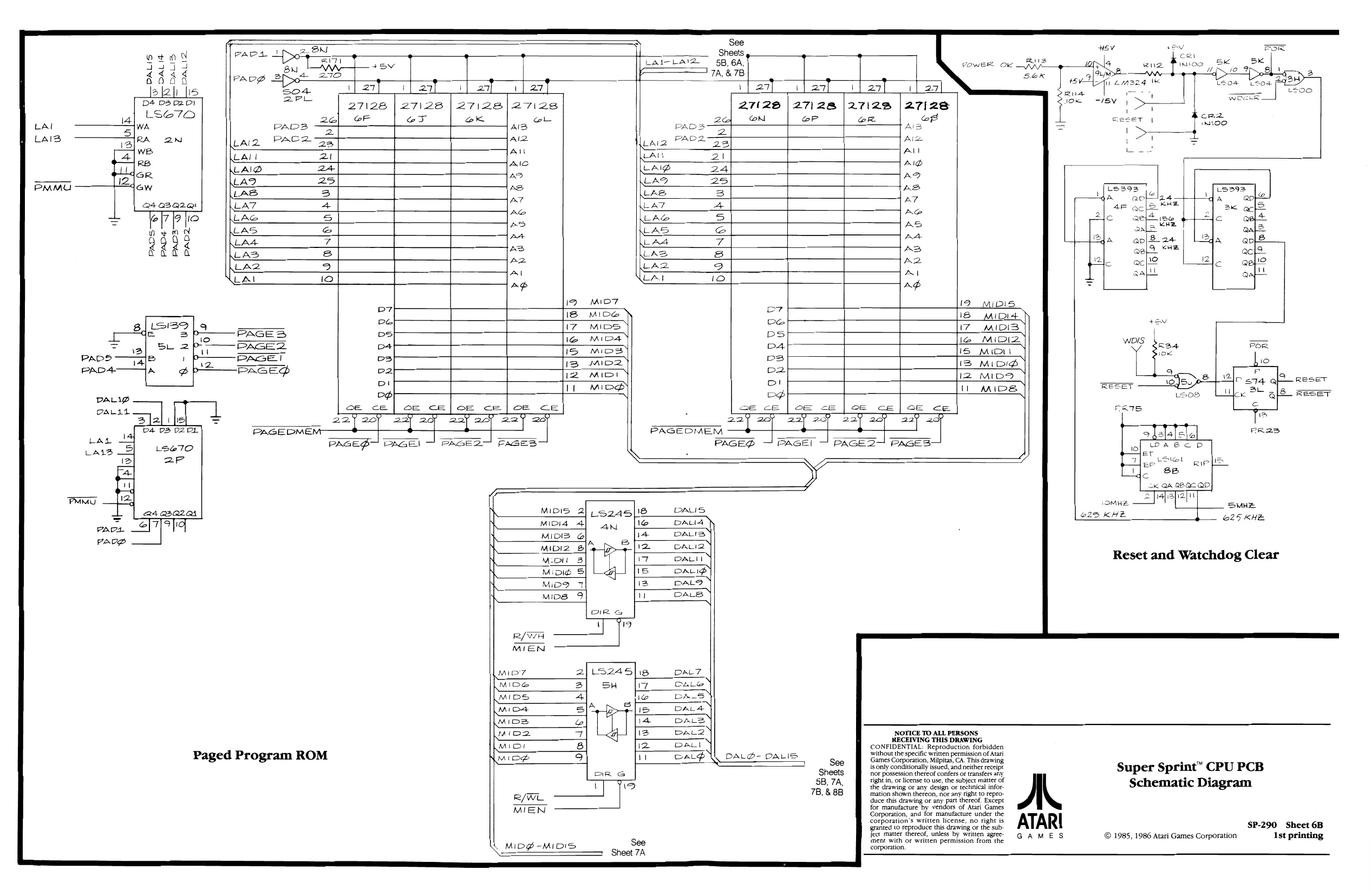
This page is a drawing, shown as the original scan.
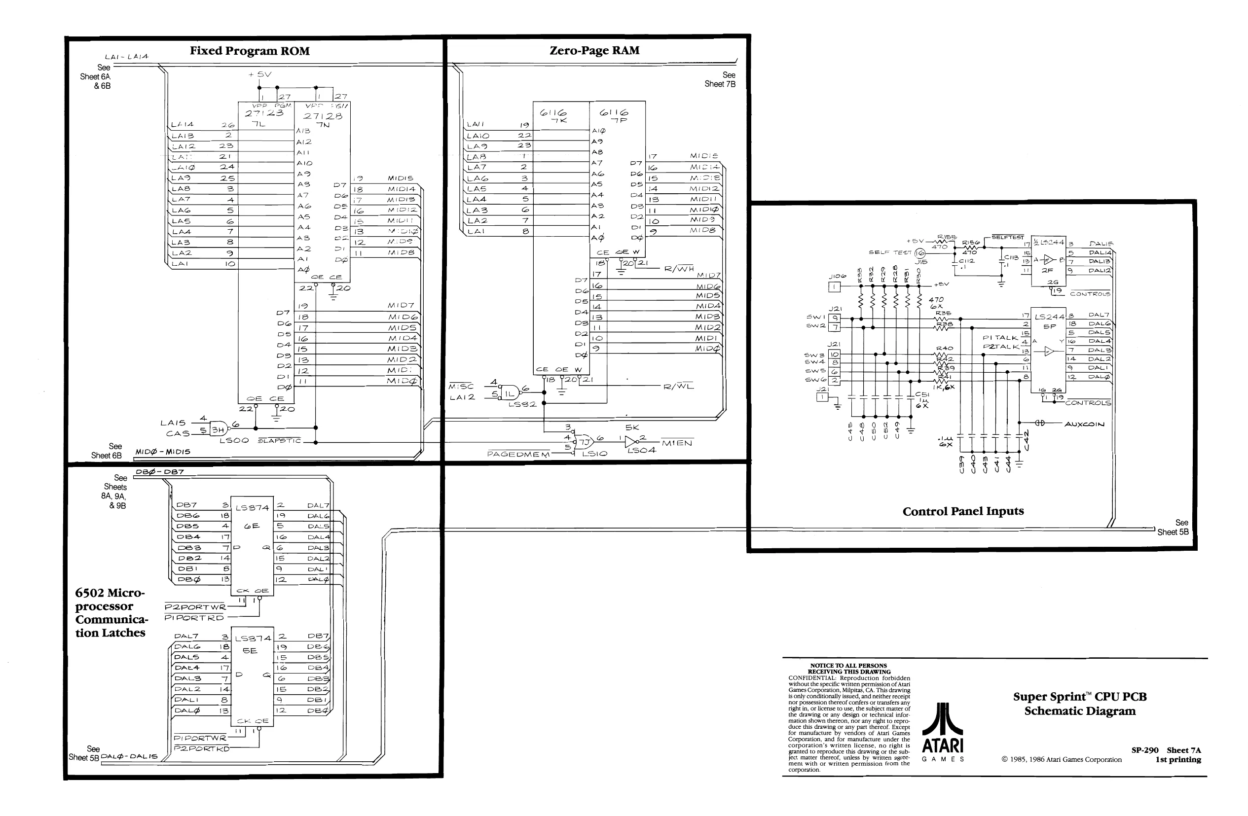
This page is a drawing, shown as the original scan.
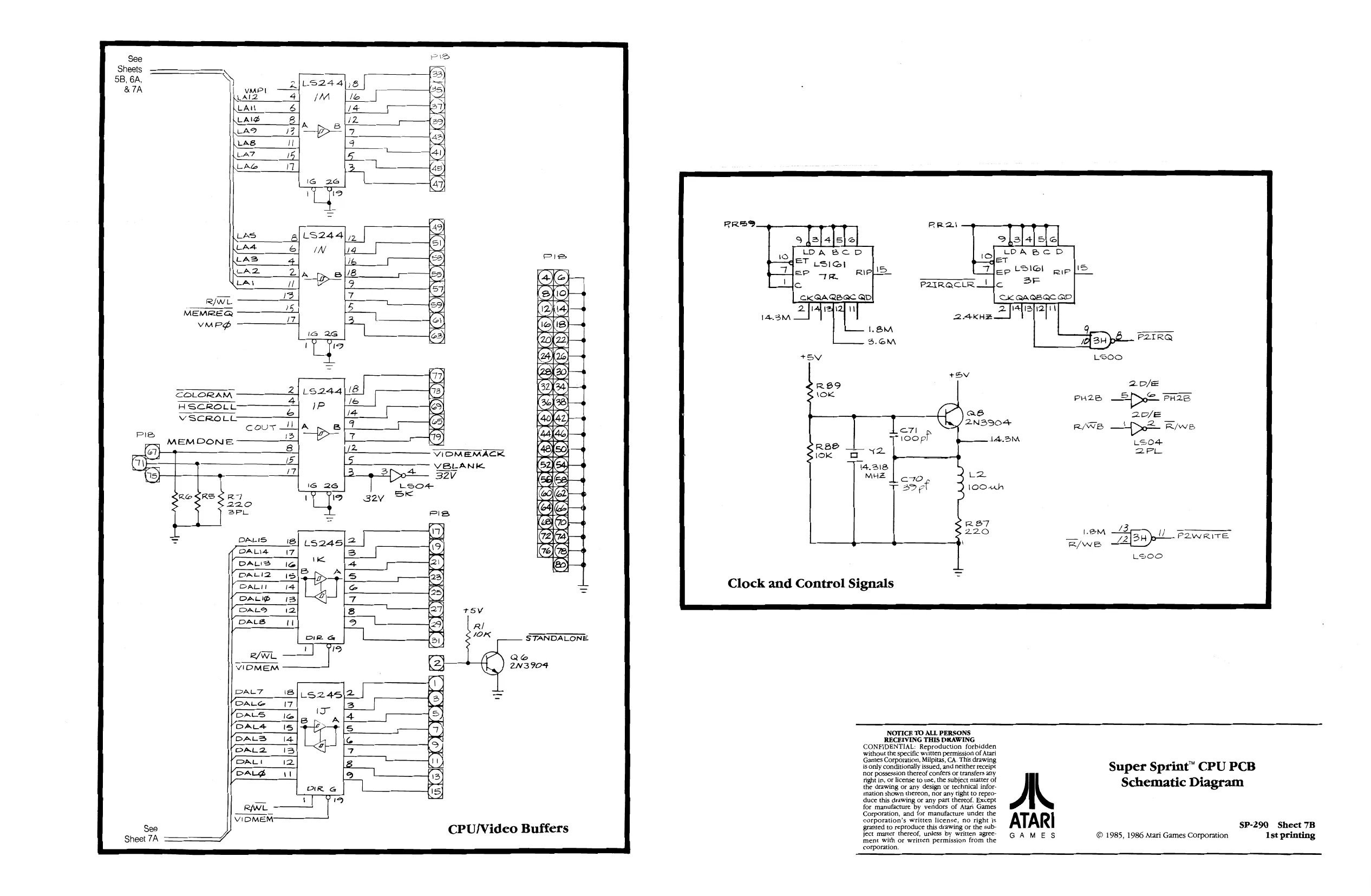
R/WL MEMREQ vuPg
COLORAM
HSCROLL-
VSCROLE
MEMDONE, cour
+
PALIS is BK
Lsot szy SS
BALA
DALS le! T-
DALI2 1s
Pau
DALIG 13) tit DAL®
DALS u ole fajofayatoyo
RW —— VIDMEM
DALTZ ORG
7 12 ViIBMEMACK
VBLANK 3B2V
is LS245) CALE (7 CALS le A BAL iS DALS ‘4 CALZ
CALI
CALS ul STANDALONE,
Qe 2N3904
CPU/Video Buffers P2TRQCLR
Clock and Control Signals
NOTICE TO ALL PERSONS RECEIVING THIS DRAWING CONFIDENTIAL: Reproduction forbidden ‘without the specific wnitten permission of Atari Games Corporation, Milpitas, CA. This drawing ‘sonly conditionally issued, and neither receipt or possession thereof confers or transfers ay right in, oF license to use, the subject matter of the drawing or any design or technical infor. mation shown thereon, nor any tight t0 reproduce this drawing or any part thereof. Except for manufacture by vendors of Atari Games Corporation, and for manufacture under the corporation’s written license, no right is ‘granted to reproduce this drawing or the subject marter thereof, unless by written agree ment with or written permission from the corporation. [By P2WRITE Loo
Super Sprint” CPU PCB Schematic Diagram
SP-290 Sheet 7B © 1985, 1986 Atari Games Corporation Ist printing
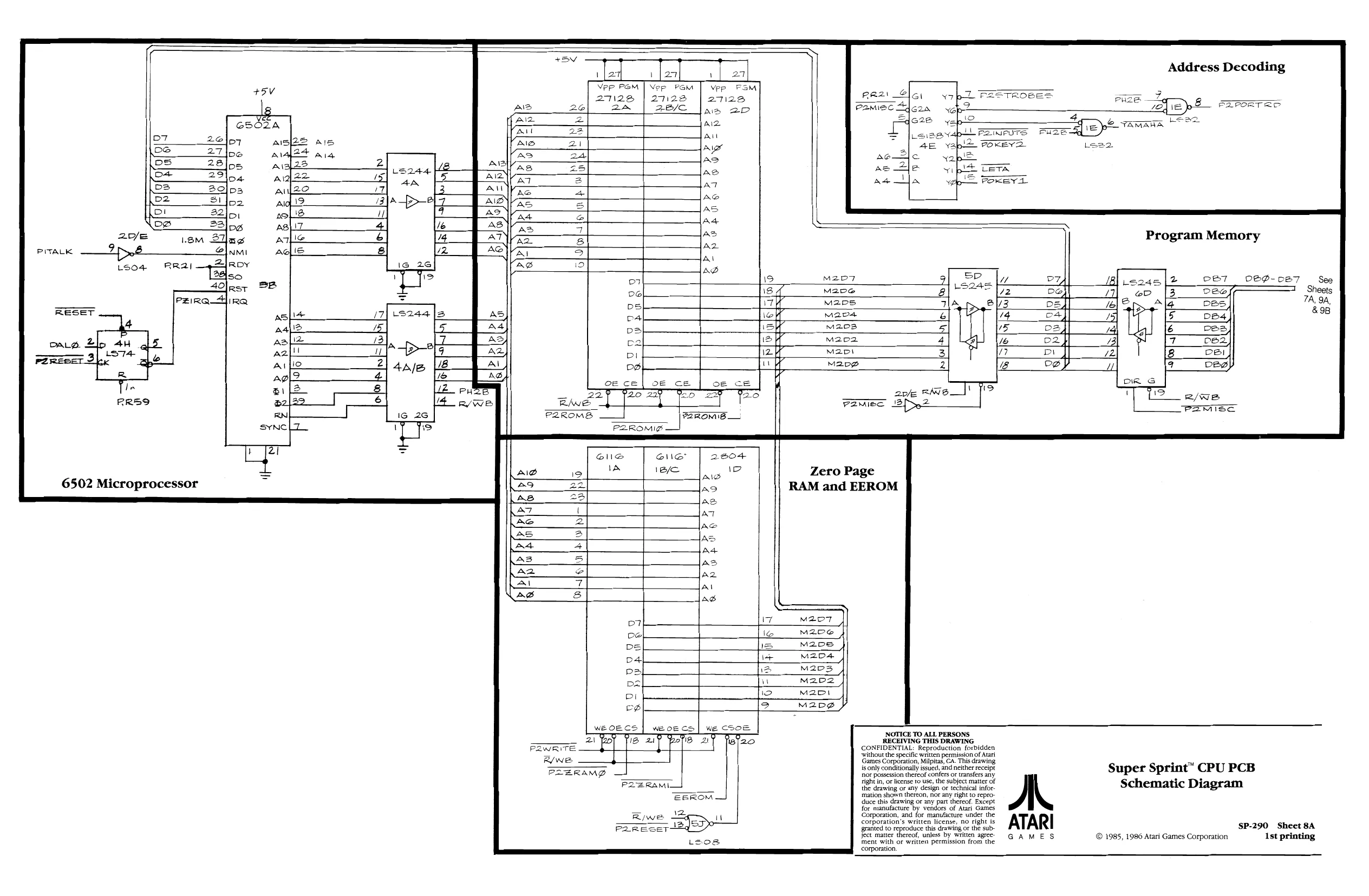
PITALK
6502 Microprocessor 3] Vfo fs fo fn]
AS
AZ
AL AD
Address Decoding
e2PORT ED
Program Memory
ce7 0EP-cB7 See Dee Sheets DES, 7A, 9A, De4 &9B
Des,
DE2,
oe 9/00] J] afS fool DBS,
P2aMIEe
AIS
Zero Page
RAM and EEROM
NOTICE TO ALL PERSONS RECEIVING THIS DRAWING CONFIDENTIAL: Reproduction forbidden ‘without the specific written permission of Atari Games Corporation, Milpitas, CA. This drawing, is only conditionally issued, and neither receipt nor possession thereof confers or transfers any right in, oF litense ro use, the subject matter of the drawing or any design or technical infor: mation shown thereon, nor any right to reproduce this drawing or any part thereof. Except for manufacture by vendors of Atari Games Corporation, and for manufacture under the Corporation's written license, no right is, granted to reproduce this drawing or the subject matter thereof, unless by written agree- ‘ment with or written permission from the corporation, U2 2/ae PEMISeS
Super Sprint" CPU PCB Schematic Diagram
ATARI SP-290 sheet A
GAMES © 1985, 1986 Atari Games Corporation 1st printing
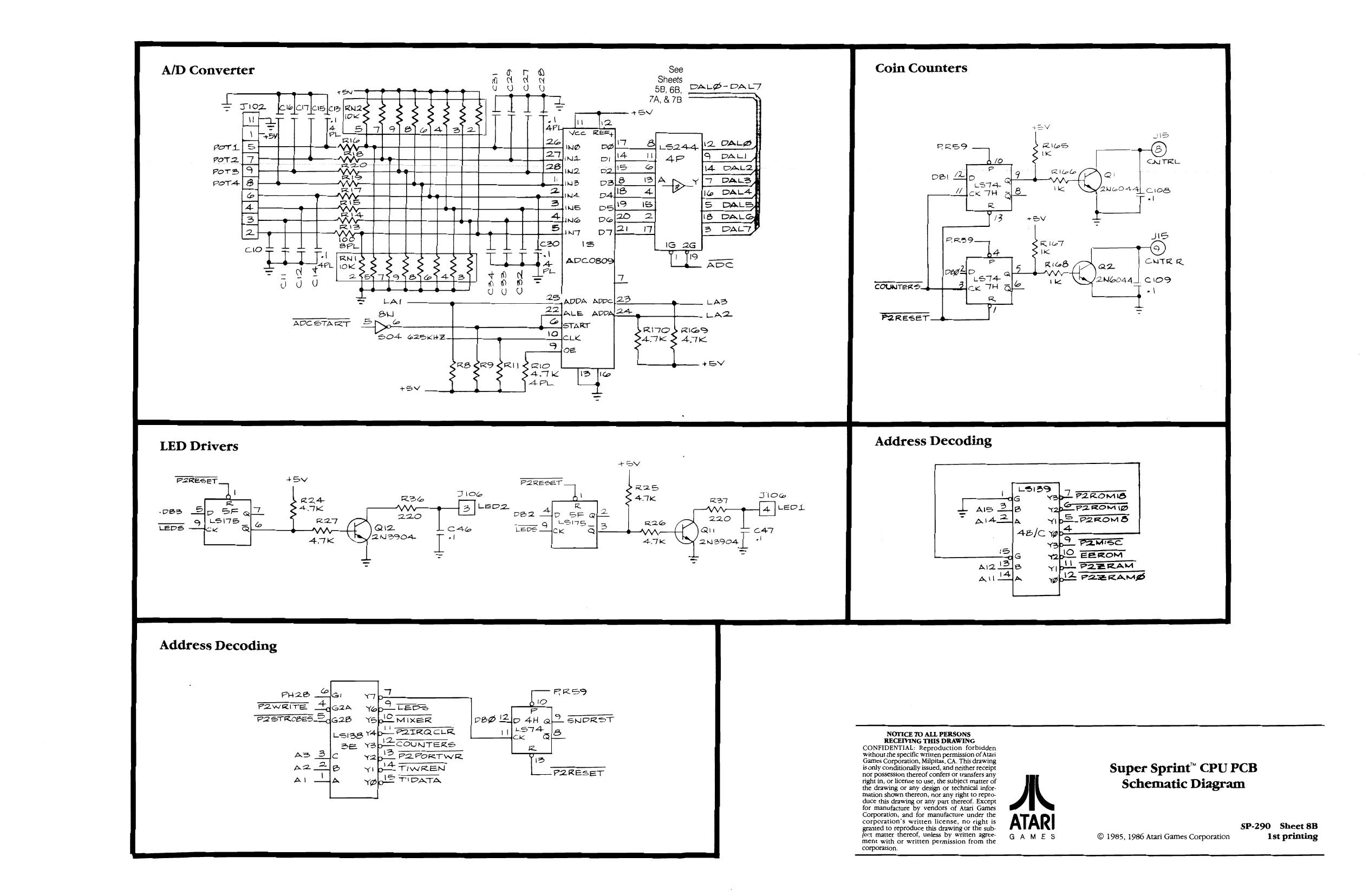
This page is a drawing, shown as the original scan.
This page is a drawing, shown as the original scan.
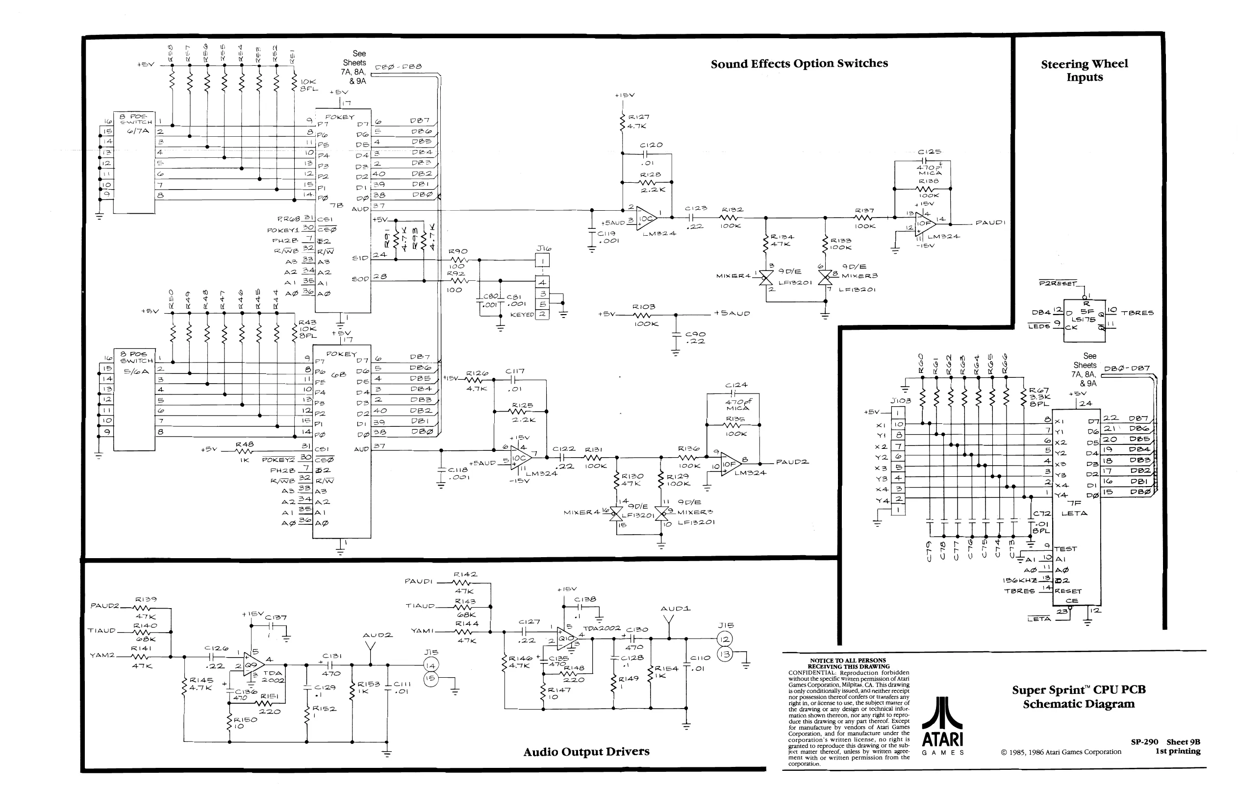
& POs SwiteH Sloan
PAUDI
KISS K Ol [efnJo [> }-[-
Sound Effects Option Switches
MixeR4.
Audio Output Drivers sce
LFi2201 Zz
Reo Rel Ro2 ROS Roa ROS
Steering Wheel Inputs
Roe TA, 8A, &9A Sheets 589-087
NOTICE TO ALL PERSONS RECEIVING THIS DRAWING CONFIDENTIAL: Reproduction forbidden ‘without the specific written permission of Atari Games Corporation, Milpitas, CA. This drawing, is only conditionally issued, and neither receipt ‘nor possession thereof confers or transfers any right in, oF ficense to use, the subject matter of the drawing or any design of technical infor. ‘mation shown thereon, rior any right to reproduce this drawing or any part thereof. Except for manufacture by vendors of Atari Games Corporation, and for manufacture under the corporation's written license, no right is ‘granted to reproduce this drawing or the subject matter thereof, unless by written agree: ment with or written permission from the ‘corporation. AL
ATARI
GAMES
Super Sprint” CPU PCB Schematic Diagram
SP-290 Sheet 9B © 1985, 1986 Atari Games Corporation 1st printing
This page is a drawing, shown as the original scan.
This page is a drawing, shown as the original scan.
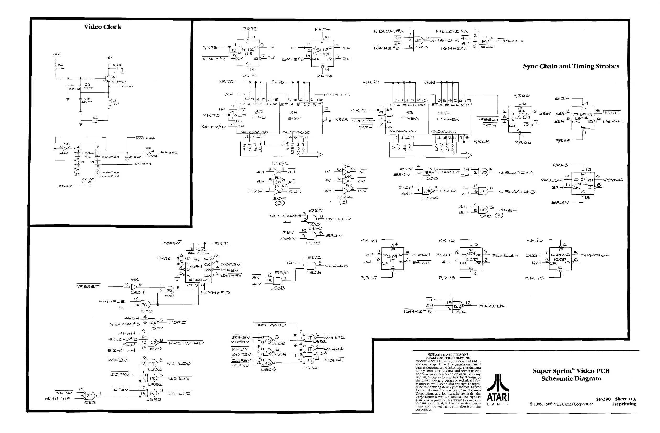
This page is a drawing, shown as the original scan.
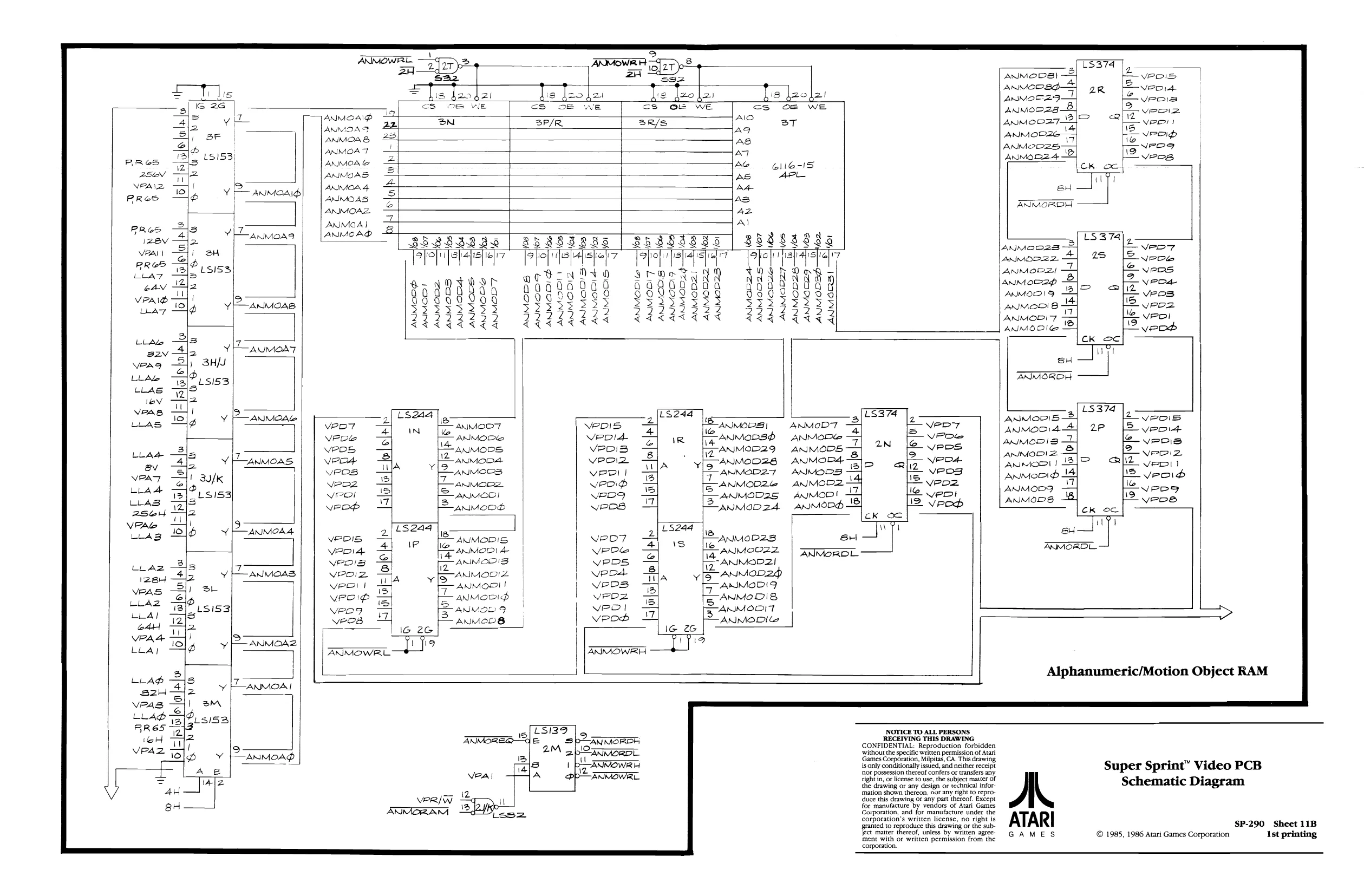
This page is a drawing, shown as the original scan.
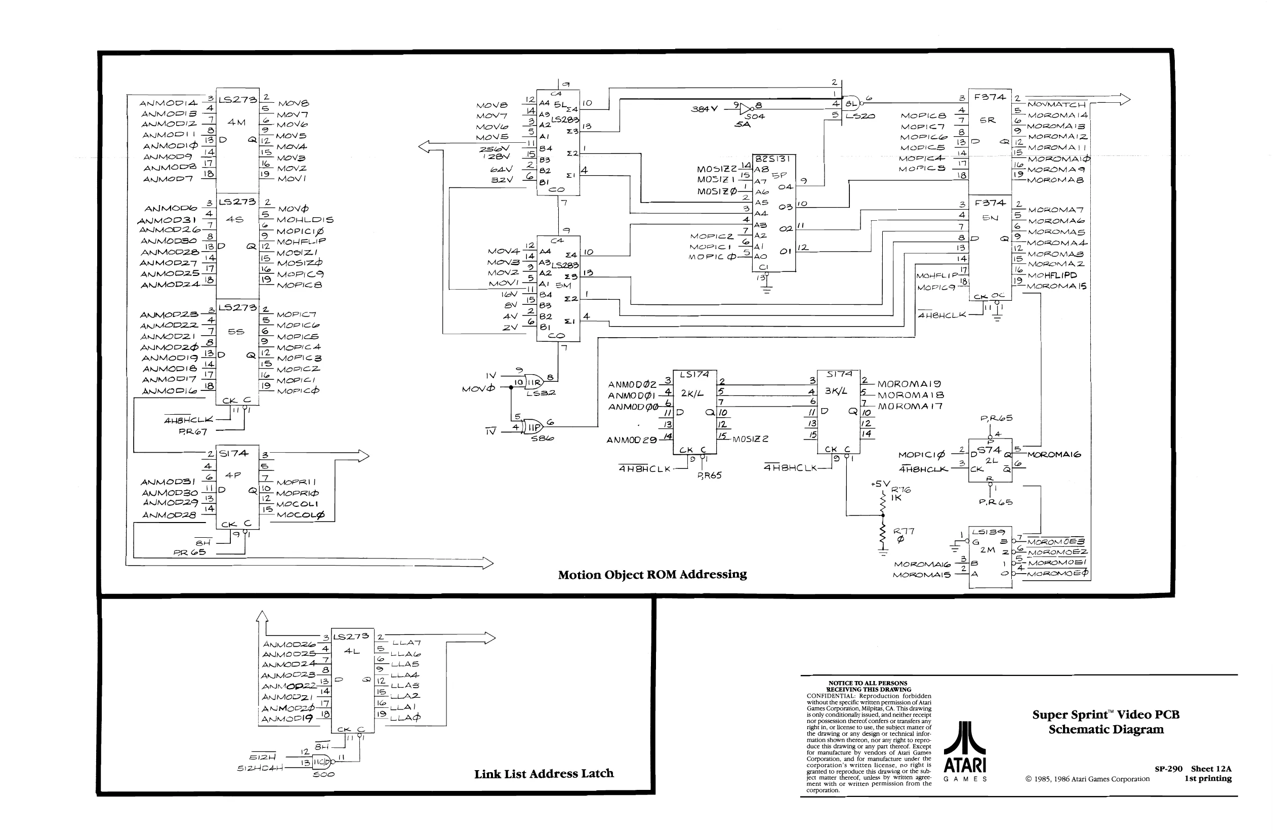
This page is a drawing, shown as the original scan.
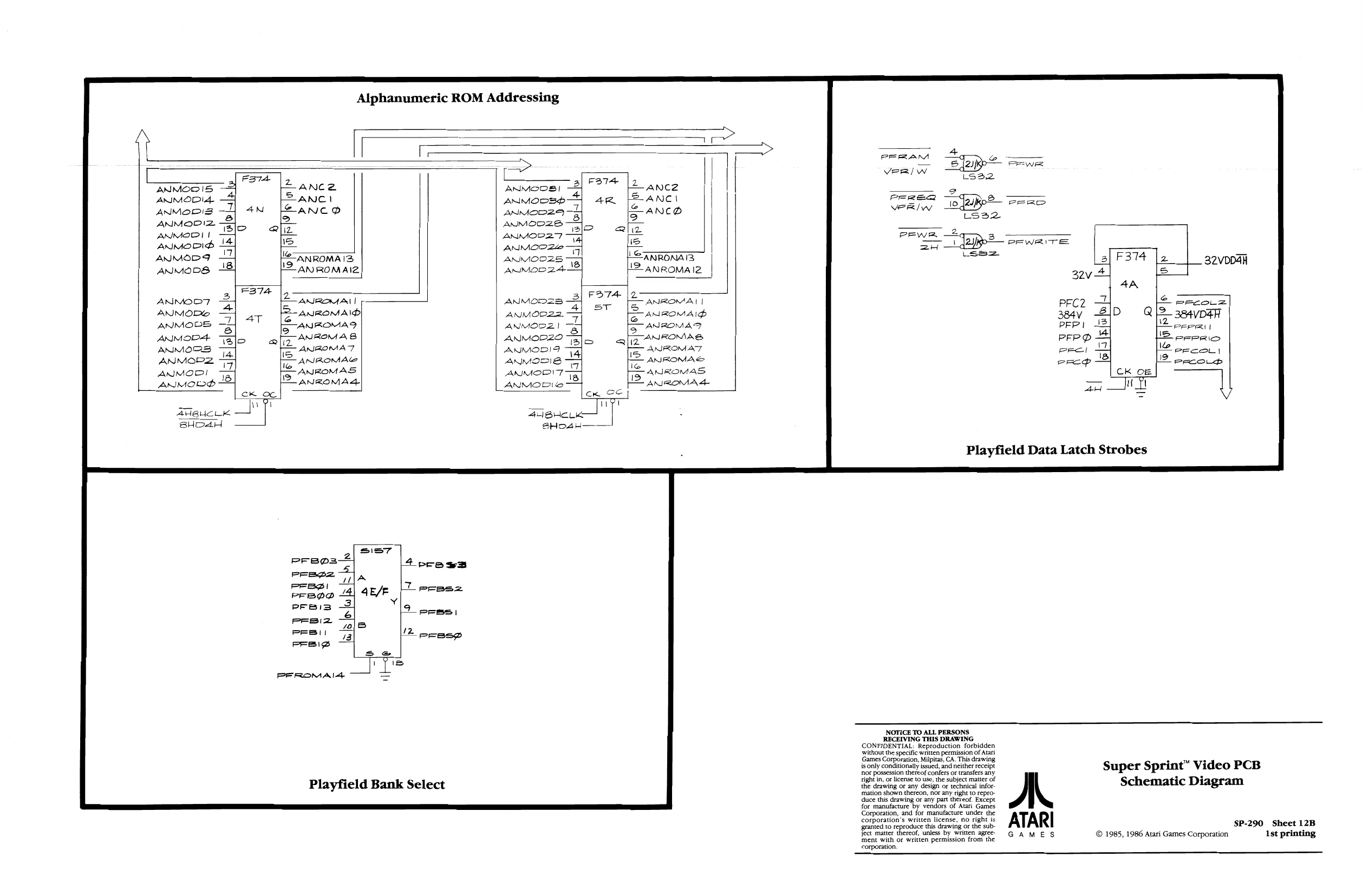
This page is a drawing, shown as the original scan.
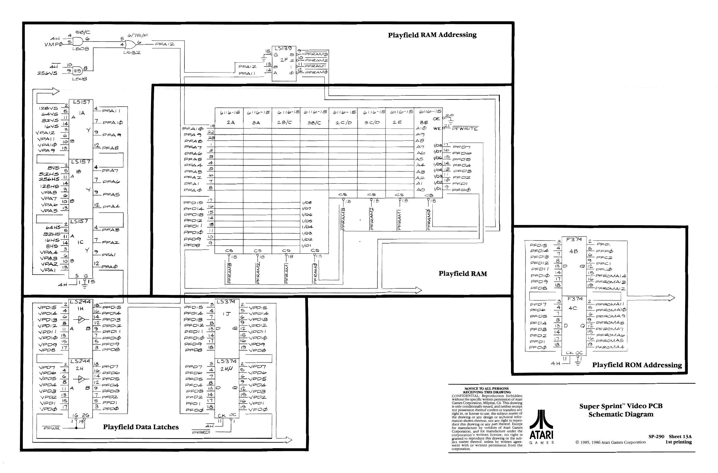
This page is a drawing, shown as the original scan.
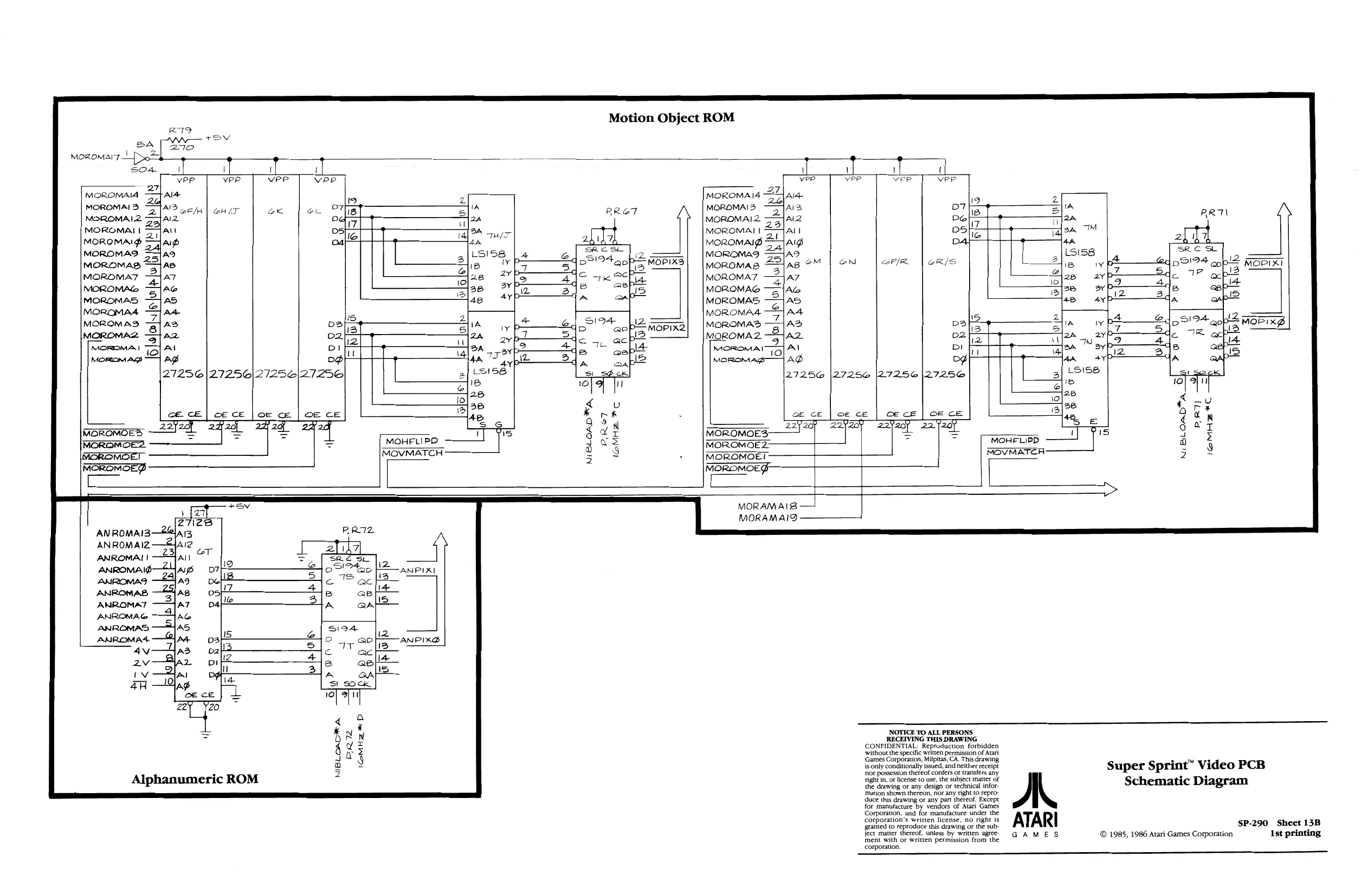
This page is a drawing, shown as the original scan.
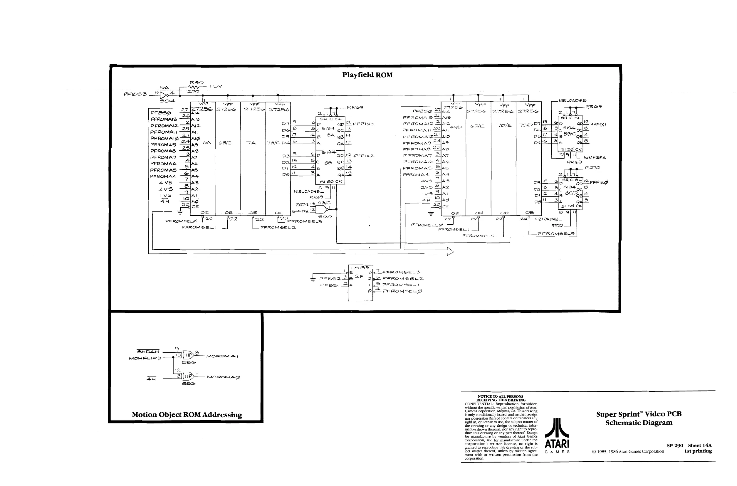
This page is a drawing, shown as the original scan.
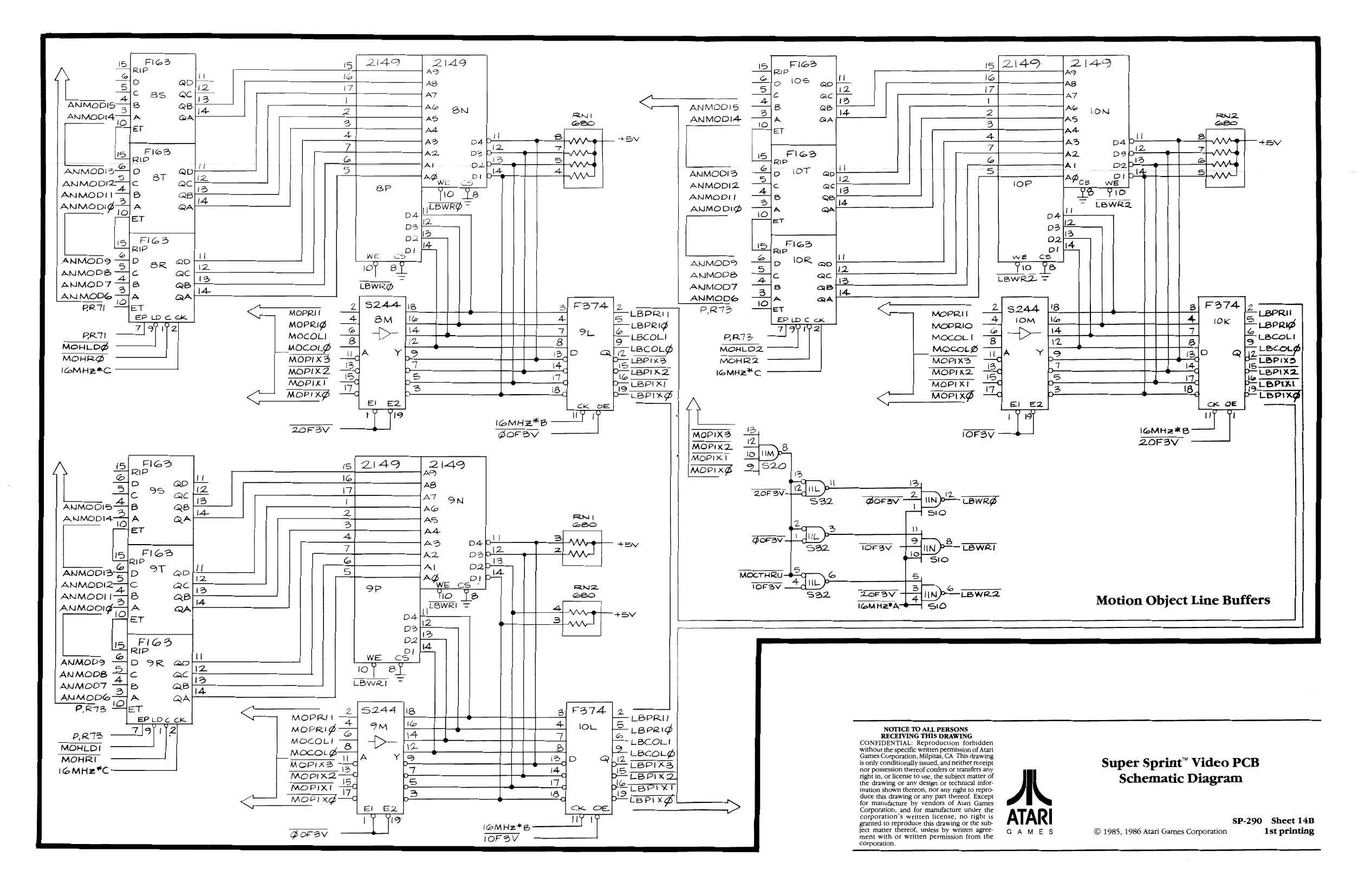
This page is a drawing, shown as the original scan.
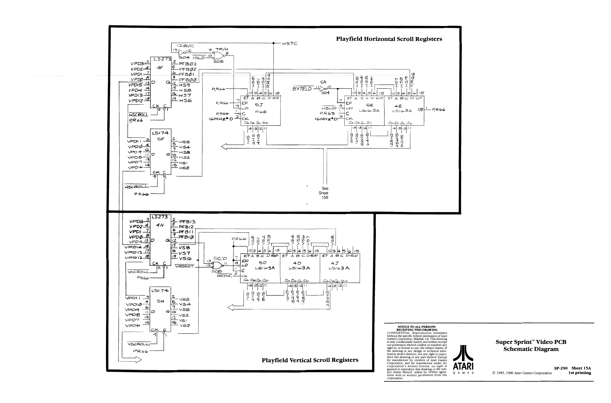
This page is a drawing, shown as the original scan.
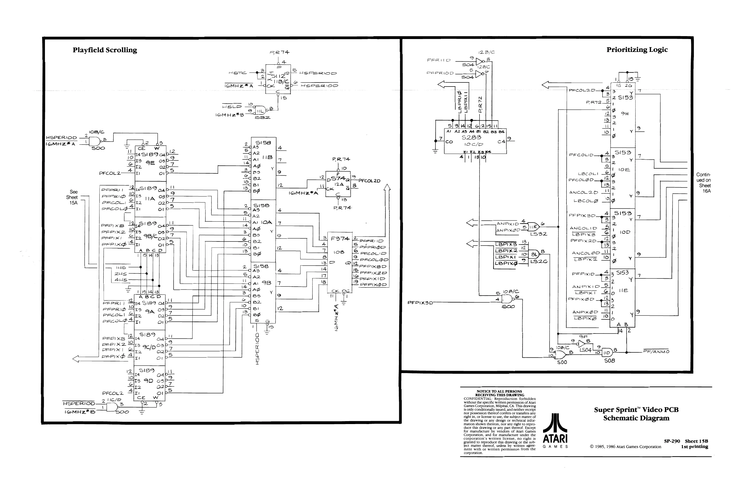
This page is a drawing, shown as the original scan.
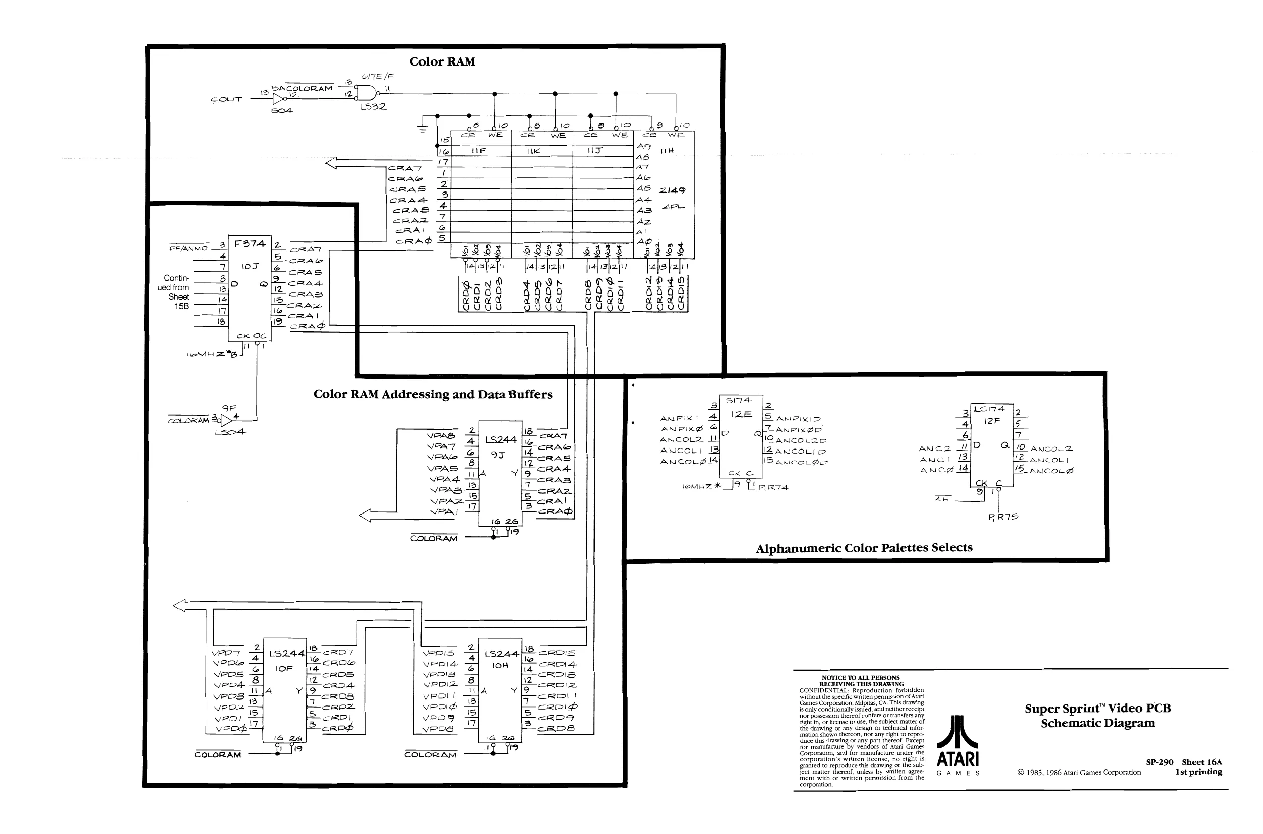
This page is a drawing, shown as the original scan.
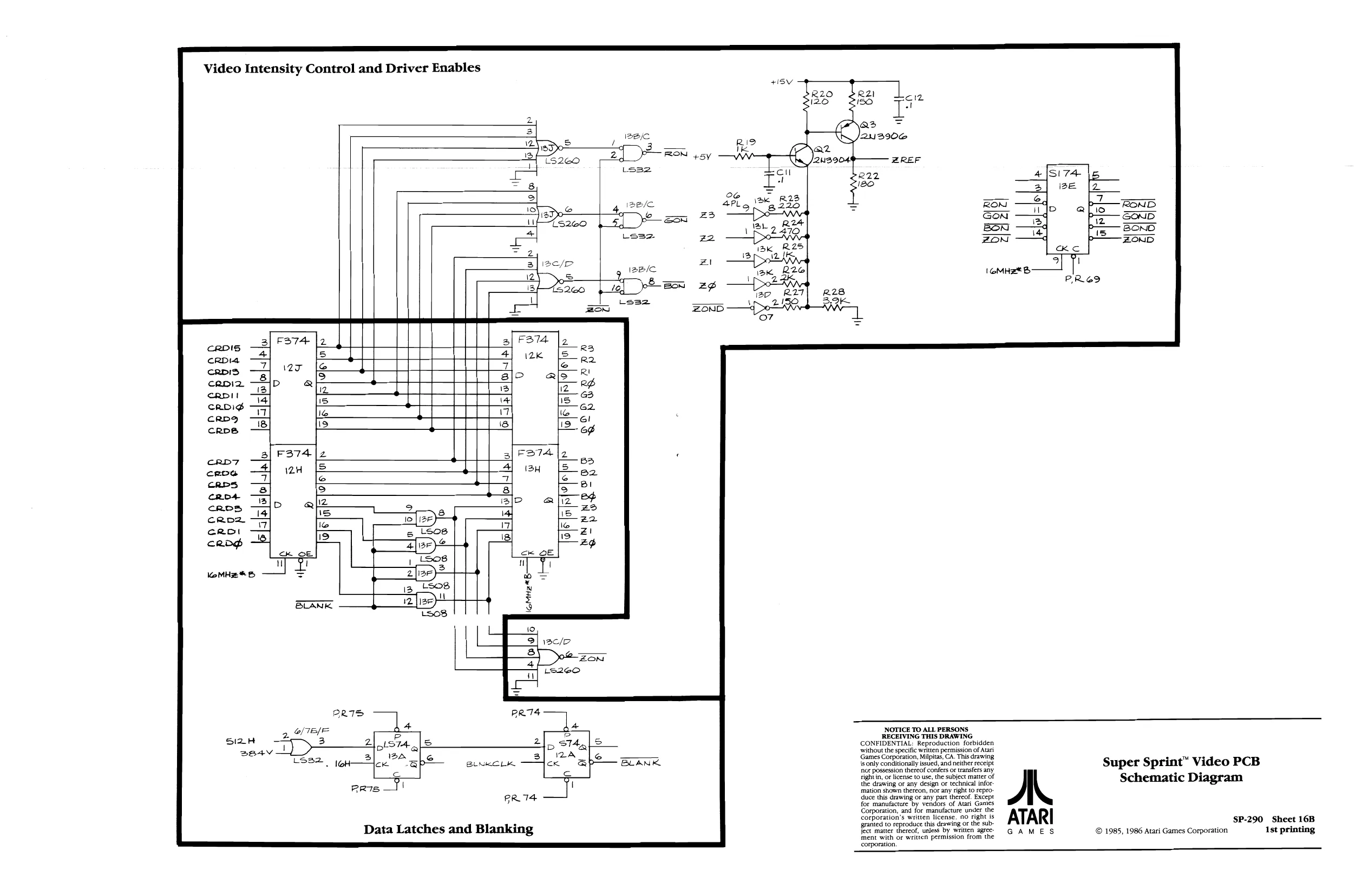
This page is a drawing, shown as the original scan.
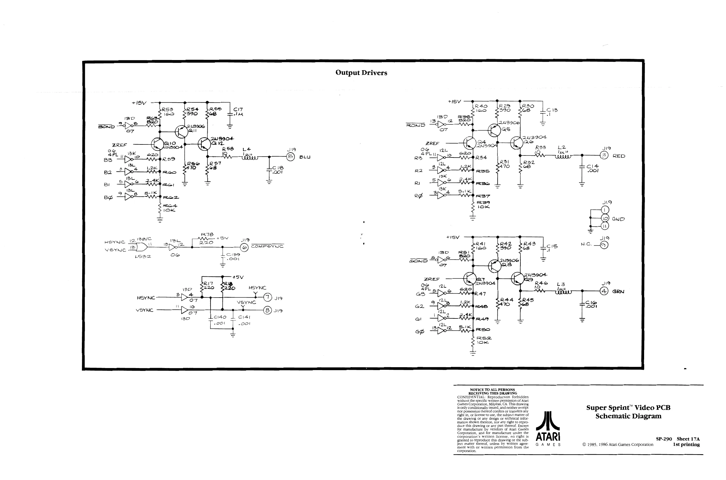
This page is a drawing, shown as the original scan.