Barrier Schematics
Barrier (Cinematronics (Vectorbeam license), 1979) · Schematics · 23 pages · 28 sections · original scan

This page is a drawing, shown as the original scan.
GENERAL DESCRIPTION
This chapter describes the principles of operation of the major circuit functions of the Vectorbeam BARRIER game. The system’s general functional description is followed by detailed circuit descriptions. Each circuit description includes simplified circuit schematics (Appendix A) applicable to the blocks under discussion. Note that all of the schematics used are very similar to the schematics used by most industrial electronics firms. The use of the wide arrowhead paths simplify the schematic bus lines.
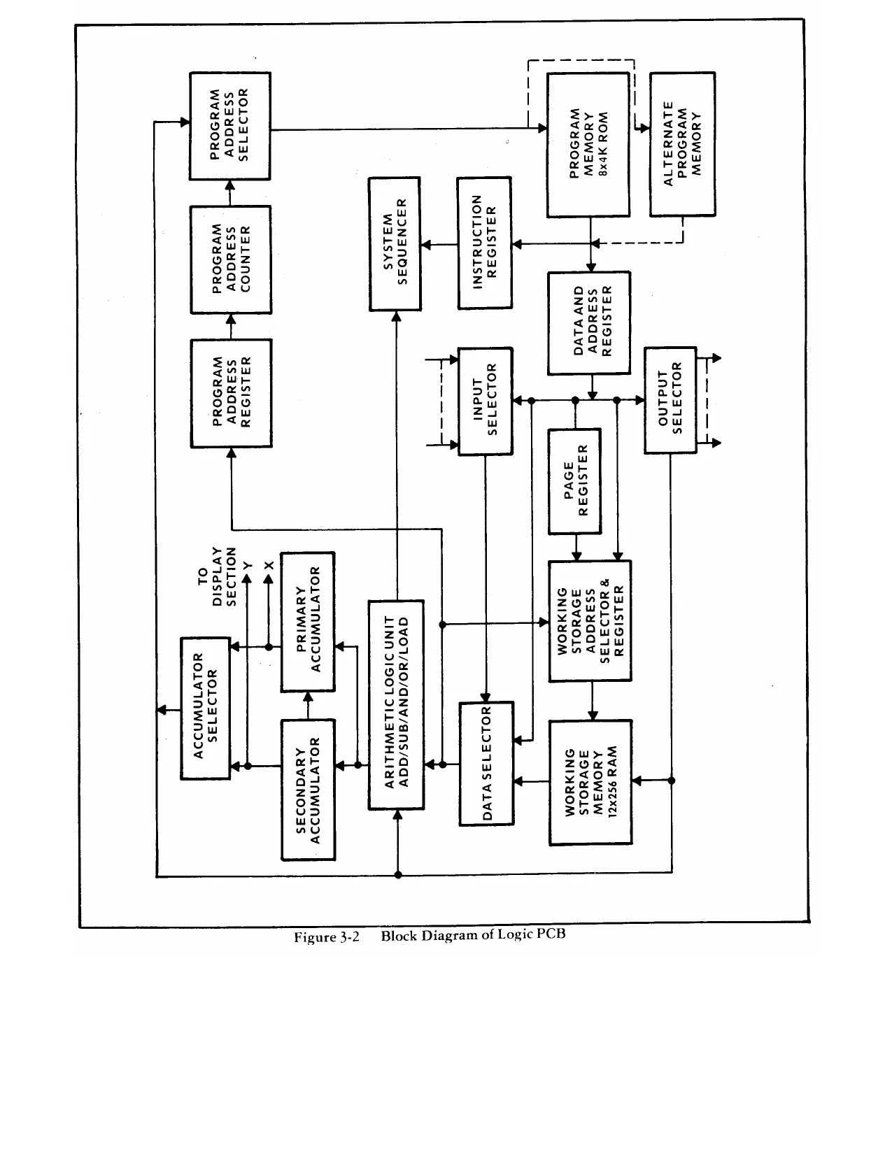
Figure 3-1 illustrates all of the major components of the Vectorbeam BARRIER game. This block diagram indicates that the logic board is separate from the monitor. It also illustrates the low voltage power supply package, the coin mechanism, the control panel and how they are interconnected. Figure 3-2 illustrates the logic board block diagram. The dash lines indicate what is used and shared by the monitor display electronics. It also indicates that which is to be only used by the display electronics on the monitor board.
MONITOR DISPLAY
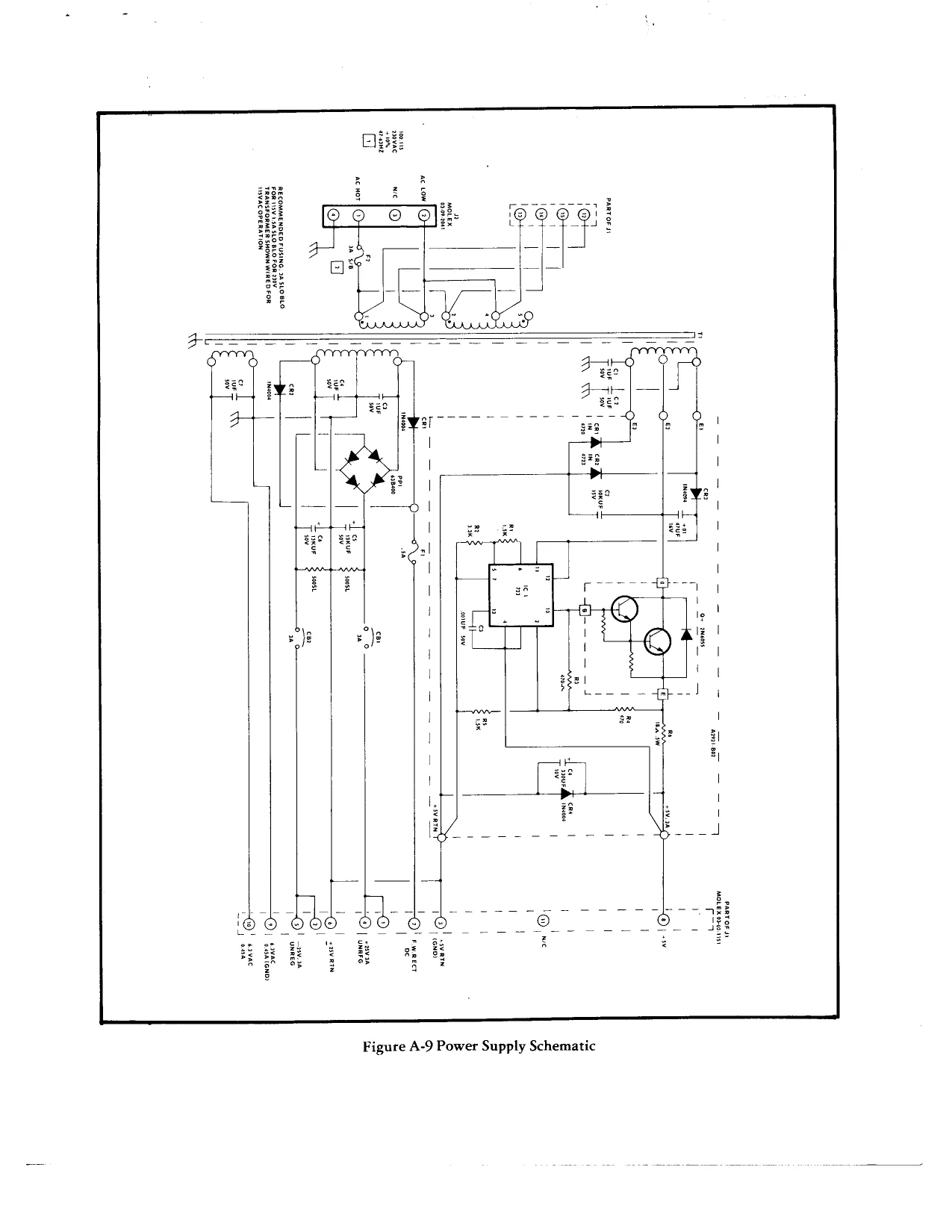
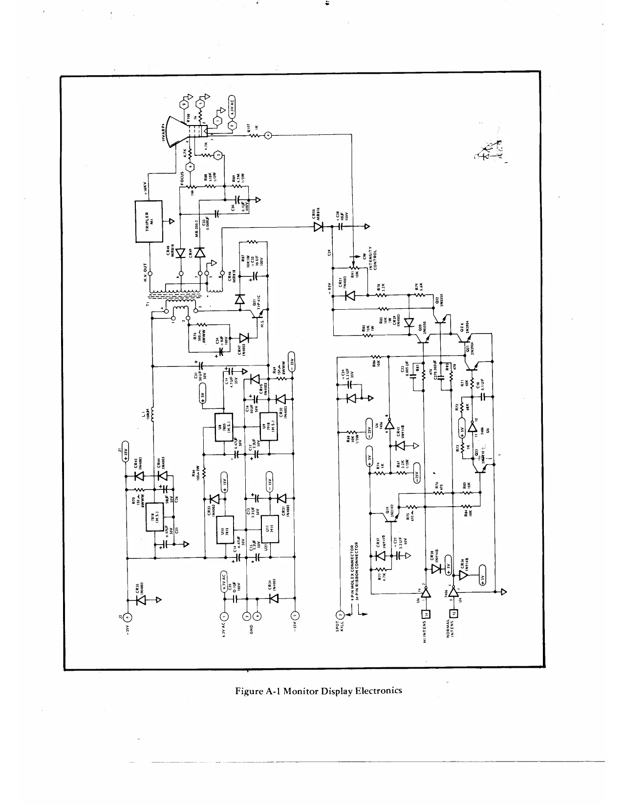
(Refer to Appendix A, Figure A-1) All monitor electronics are self-contained on a single printed circuit board. All low voltages supplied to this board originate from the power supply package located inside the game cabinet. All troubleshooting and maintenance procedures are located in the MAINTENANCE chapter of this manual. The Vectorbeam monitor is unlike the conventional TV monitor. It is a vector system that displays vectors (lines) generated from X-Y coordinates received from the logic board. The horizontal points are X and the vertical Y (width and height respectively). The X and Y logic signals originate from the logic board, discussed later. The +25 volts and 6.3 volts AC and the +25 volt spot kill originate from the low voltage power supply. The +25 volts is a DC voltage rectified and filtered in the supply package. The 6.3 volts AC is used as the heater voltage for the CRT display. On Figure A-1, in the upper-left hand comer, voltages have been regulated by the three terminal regulator devices. For example the +25 volts is regulated by a 7818 and a 7918 respectively down to +18 volts used by the oscillator. Transformer T1 provides the means to supply the CRT grid and anode voltages. The +25 volts is also regulated to +5 volts used for the logic circuitry included in this drawing. The circuit connected to the primary of T1 (a high voltage transformer) form an oscillator which induces the necessary high voltage at the secondary of T1 The frequency is set by the T1 transformer characteristics - The output of the T1 is then rectified. The highest voltage winding is connected to the tripler M1 which raises the output voltage of this transformer and rectifies it to +18 K volts, for the CRT anode. At pin 6 the negative pulses are rectified and applied to a 1 megohm potentiometer FOCUS control which applies the grid bias at pin 4 of the CRT. The positive pulses are rectified at pin 7 of the T1 transformer as the grid 2 bias for the CRT whereas the CRT at pin 2 is at ground through register R108. The heater pins 1 and 8 of the CRT are connected to ground and pin 1 of the PCB respectively. The +25 volts is also regulated down to +15 volts for the DAC’s by device U10 and U11 (7815 and 7915 respectively). The secondary of Tl (pins 5 and 8) develop the necessary voltage to produce a +90 volts DC rectified by diode CR50 and filtered by capacitor C28, This +90 volts DC is used by the modulating circuit for the CRT display. The lower half of the drawing consists of the spot kill circuit and the intensity modulator circuit. The intensity modulating circuit is comprised of two individual circuits. One input is the high intensity and the other the normal intensity. These two inputs are connected to the high and normal intensity transistor drivers Q20 and Q21 and the hex inverter U6 (7406). Both circuits are identical. For example, in this explanation the high intensity circuit is described: In the high intensity circuit when the input goes high at pin 1 of U6 the output at pin 2 goes low. With this low signal, Q20 is turned off from an on state, and the collector of Q20 goes high. Assume that switching transistor Q24 is turned on. The NORMAL INTENSITY input is always on when the display logic is operating properly. A low input at PCB connector (pin 12) is inverted by hex inverter 7406 which turns on transistor Q22. Device Q22 completes the current path through the intensity control (R91) to ground via resistors R78 and R79 and collector to emitter of Q22. This condition applies a voltage less than +90 volts corresponding to the setting of the intensity control, to the CRT cathode. When a higher intensity is required the HIGH INTENSITY input (pin 14 of the Display PCB) goes low turning on Q20. With Q20 turned on the current path from the +90 volts line in through R91, diode CR39 then finally through the collector to emitter of Q20 to ground. This condition reduces the voltage at the wiper of R91, therefore increasing the intensity of the electron beam. The NORMAL INTENSITY input should always remain low providing some sort of constant electron beam. When the —25 volts is removed, pin 9 of U6 goes high and pin 8 goes low, which immediately tums off Q14 eliminating the chance of a spot. The U6 device is an open collector evice requiring a pull up resistor such as R86 at pin 8. The high side R86 is connected to a voltage source at pin 3 of Molex connector J2. +25 volts unregulated and unfiltered.
Another spot kill protection circuit (Q21. Q23 and U6) keeps Q14 on when either intensity input is high but when both inputs are low it provides a 2 millisecond turn-on time for Q14. After the 2 millisecond period the Q21 device tums on removing the current path through Q20 and Q22 by turning off QI4. This is accomplished when pins 2 and 4 of U6 are both high which turns on Q23. inverts at pin 10 of U6. Pin 10 of U6 as it switches from a low to a high is initially at ground. then gradually goes positive at C18, until after approximately 2 milliseconds it is positive enough to turn on Q14.
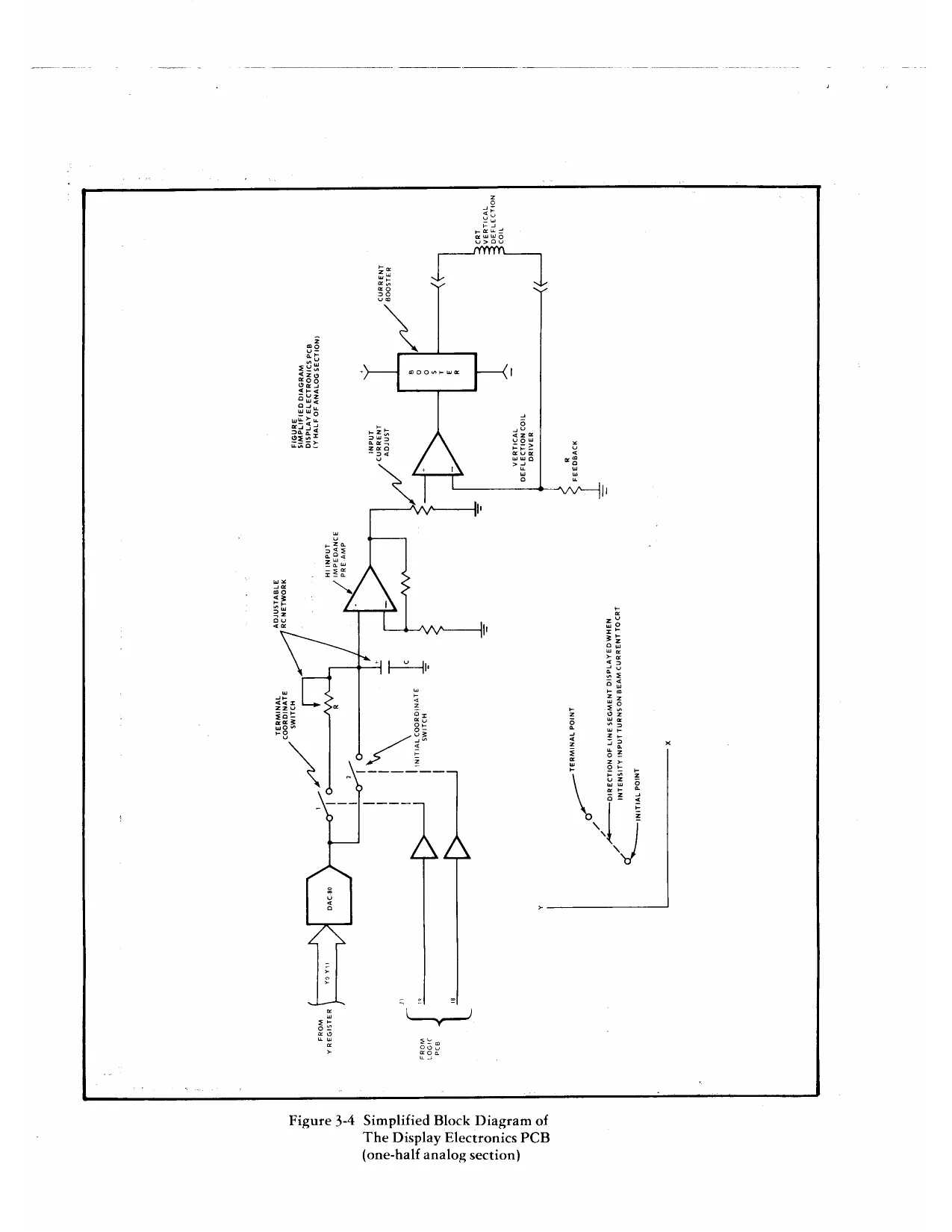
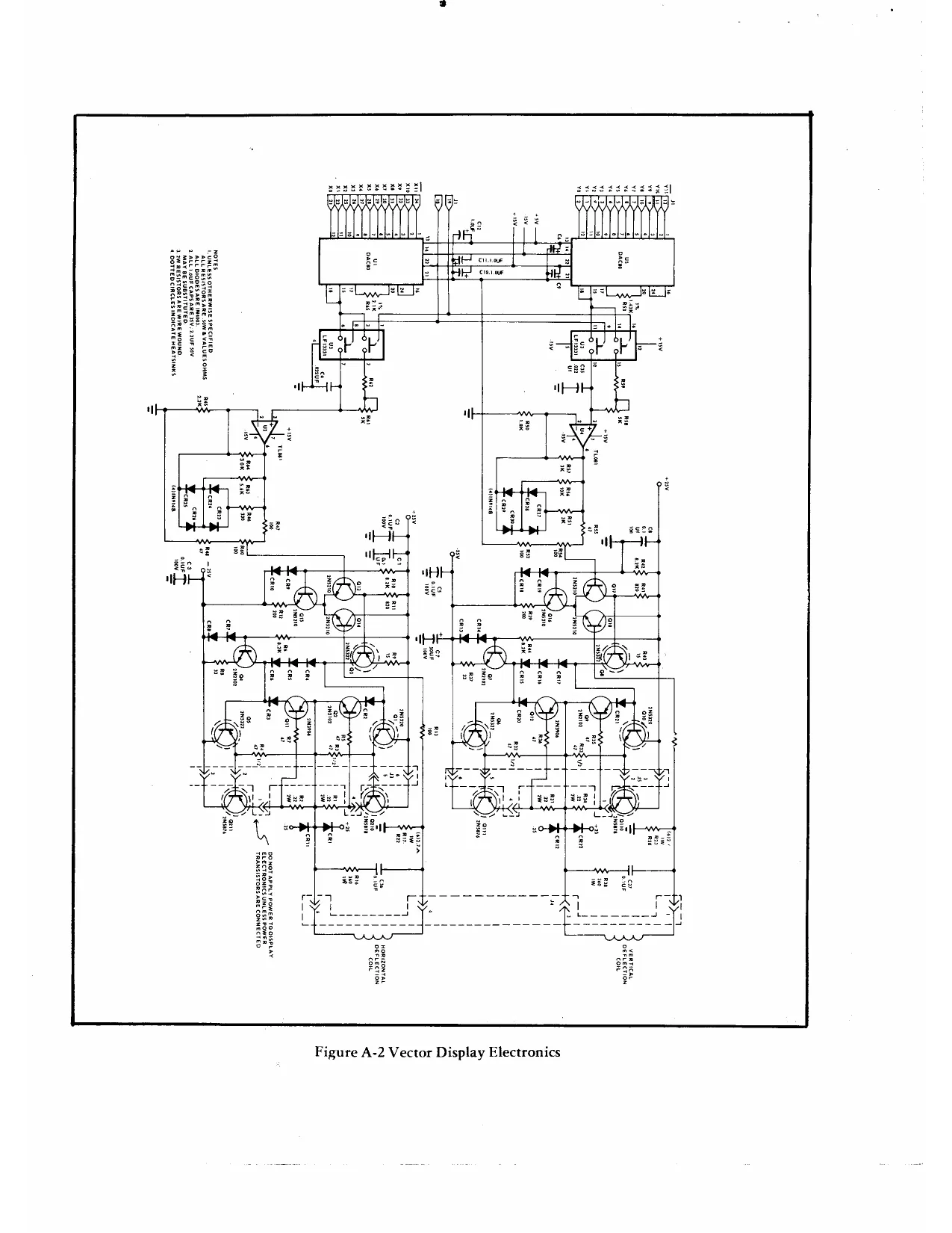
(Refer to Appendix A. Figure A-2) The schematic of Figure A-2 illustrates wo identical circuits, one for the Y and the other for the X coordinate. For purposes of this explanation only the upper halt will be discussed (the Y coordinant circuit of Figure 3.4). Beginning with the inputs we have 12. 6 inputs to DAC U5 defining the Y coordinate. These DAC’s generate approximately 4096 (4K) different positions on the screen for the Y coordinate, likewise 4096 for the X coordinate at the lower half of the circuit. Supply voltage to these two DAC’s (UG and U1) originates from the +15 volt regulators of Figure Al (U10 and U11). The analog output of DAC US enters the non-inverting input of amplifier U4 from either the analog Switch 1 or th analog Switch 2. Assume that 4 volts at the analog output (pin 15 of U5) and that analog Switch 2 has been enabled. The 4 volts applied to the input OP-AMP U4 also appears across capicitor C35. The output voltage at the circuit of U4 also appears at the wiper of potentiometer R54. The voltage at this wiper is applied to a discrete differential amplifier circuit comprised of device Q16, QI7 and QI8. The +4 volts turns on Q17 which also. turns on transistor Q8. The input to this transistor is the output of the differential amplifier of Q17 and Q18. This output is then urrent boosted by the Q10 and QELO devices for the positive transistion or by the Q6 and QUILL tor the negative transitions. Devices Q9 and Q12 are the overload protection. The current then flows through the Y (vertical) deflection coil and back to the inverting input at the hase of QI8 in the differential amplifier circuit which nulls out. providing a perfectly balanced current injection. circuit. Nothing is displayed on the screen since there is no signal entering the normal or high intensity inputs of the modulator circuitry of Figure A-L. Switch 2 opens leaving the charged capacitor C35 with the initial voltage, which is the initial point of the line segment to be displayed on the CRT after Switch 2 is opened (Switch 1 also remains open). The terminal point of the line segment is entered into the Y register of the logic board and then loaded into the DAC. Assume 5 volts at the output of the DAC. Switch 1 is energized, making contact and appling the 5 volt output from the DAC to the non-inverting input ot U4. This new voltage is across the RC network comprised af R58. R59 und C35. The modulating circuits of sheet 1 of 2 turns on the clectron beam current to the CRT providing a display from the initial point (voltage across C35) to the terminal point. voltage which has been loaded into the DAC trom the Y register. The transition from the initial point to the terminal point appears as a straight line, The rate ar which this line seyment travels is determined by the RC network at the input of U4, When the register is changed te a new point, Switch L opens and Switch 2 value across C35. The initial voltage across C35 4s never displayed on the CRT until a signal at the intensity modulator input turns on the clectron beam current to the CRY. The lower half of this section for the X coordinate 1s identical,
THE VECTOR GENERATOR
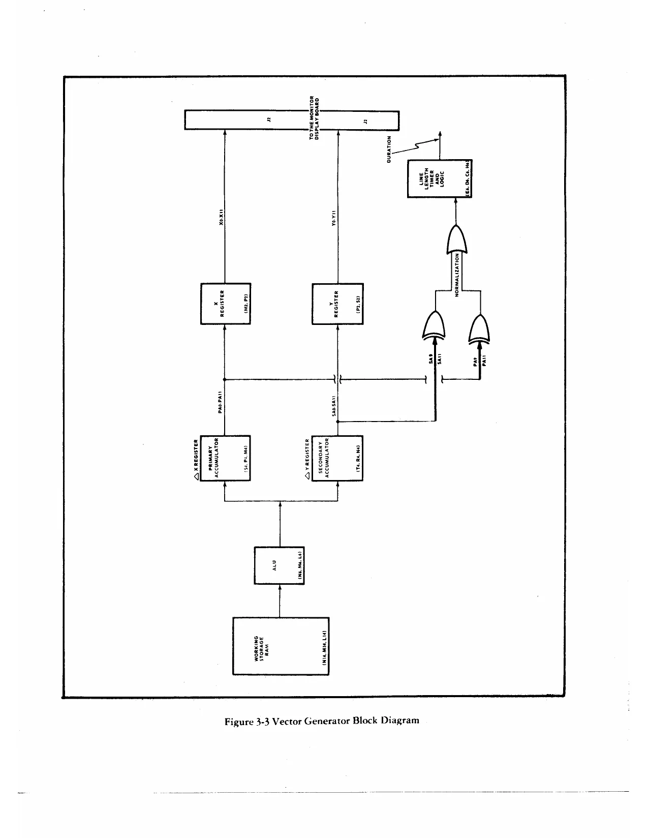
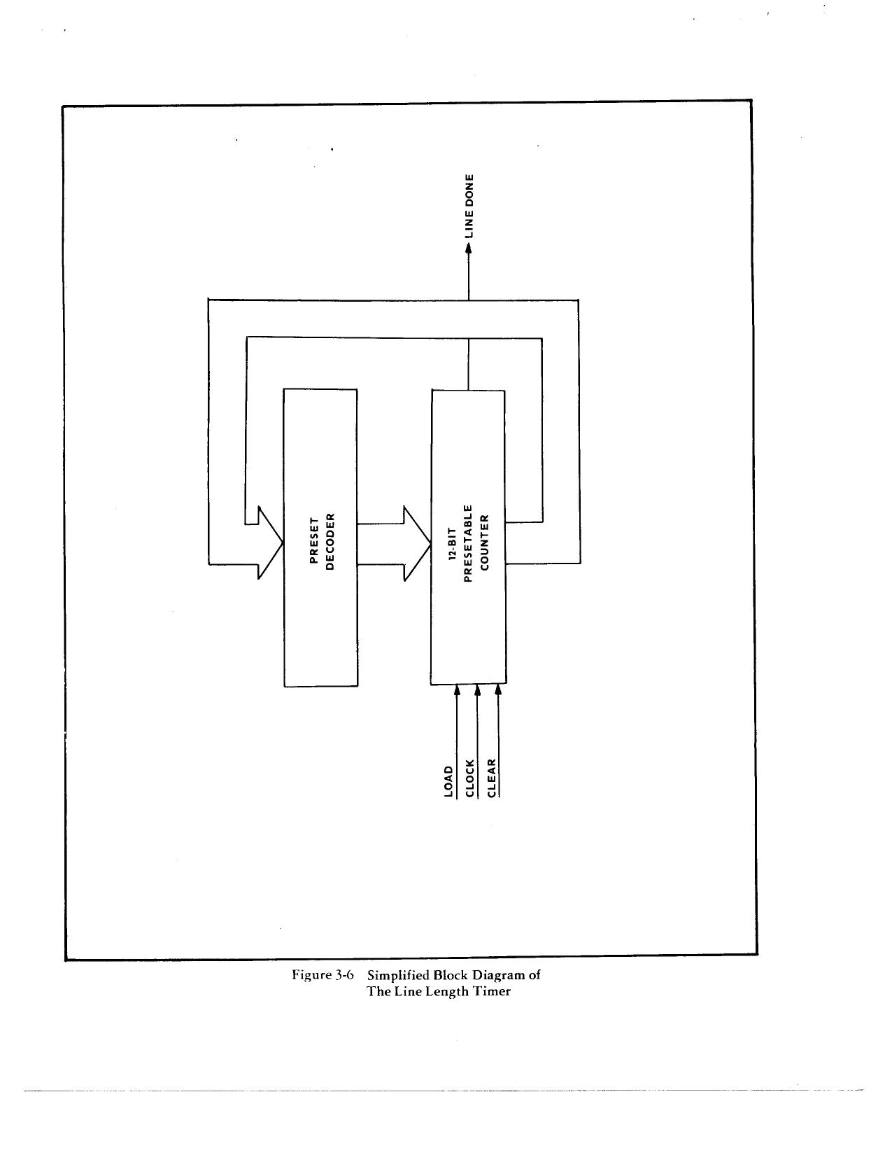
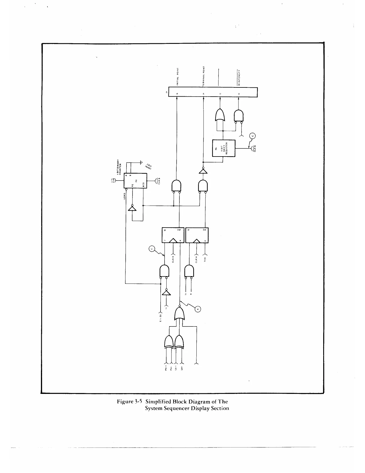
The vector generator is the digital section ot the vector display electronics located on the logic board. As illustr ted in Figure 33. it shows the working storage register. program memory, arithmetic logic unit (ALU). the primary and secondary accumulators together with the accumulator selector and the system sequencer logic, The remaining logic circuitry which is the X and Y register and the line length timer are primarily used for the display functions and are not shared with the game logic. Figure 3-4 extracts the digital display electronics from Figure 3.3 simplitying its explanation. The line length timer included in Figure 3-4 is divided into the decoderand
counter of Figure 3.5, The purpose of the line length times
is to determine the duration of closure to the clectron beam. switch which allows a vector to be displayed on the CRT The 12 bit presetable counter comprised of D6 and C6 is initially cleared (CLR) which sets it to zero, Tt then counts at the rate of the clock (CLK 8). The output of the counter addresses the preset decoder which produces outputs to the counter which are the preset inputs to the counter whenever a load signal goes low. This enable is removed when the line length counter reaches a maximum count.
THE GAME LOGIC
Program Memory closes which places the new
‘A PROM PCB is temporarily used in place ot the standard ROM devices (8. 8 X IK EPROMS). This PCB is remote trom the logic PCB mounted next to the audio PCB. When ROM's (permanent devices) are developed they are to be installed in their appropriate sockets and remove the PROM PCB.
The program memory is comprised of 2, 8 X 4K ROMS with two pages of memory in each: 1 even chip, 1 odd chip. The odd chip contains the odd memory and the even chip contains the even memory locations.
The Program Address Counter (Refer to Appendix A, Figure A-5) The program address counter is comprised of 4-bit binary counters S11, R11 and P11 (74LS163). These counters are presetable by the states of inputs at pin 3, 4, 5 and 6. The preset inputs originate from register devices P13 and R13 (748377 and 74LS194 dual latch registers). These registers are loaded with the data from the output of the data selector (LO-L11) which originates from either the RAM or the ROM memory (see Figure A-6). When the register is loaded, the output presets the input to the program address
counters. This preset input is loaded when pin 9 of each of
the counter devices goes low. This preset input is the initial point from where the counters begin to count. The output of the program address counter, a sequential scheme, addresses the ROM program memory whenever the program address selector selects bus B, When A is selected it automatically is tied through the address bus to the ROM program memory. These counters carry output of each device (S11 the least signigicant device and P11 the most significant). The carry output of S11 triggers the R11 counter. Counter R11 reaches the count of 16 producing high carry output as a dignal t pin 10 to P11. This program address counter is capable of addressing all 4K words of memory in the ROM program memory.
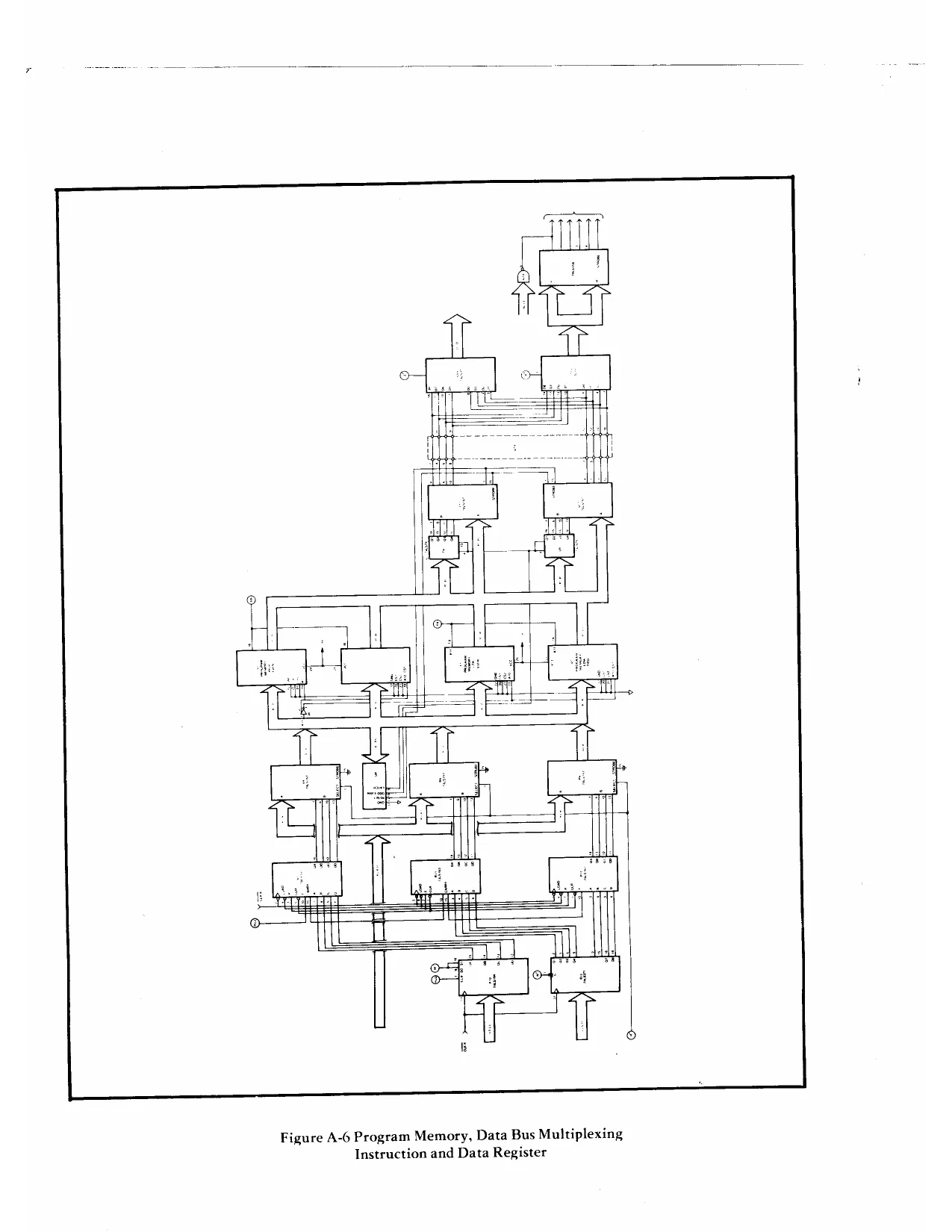
Program Memory Data Bus Multiplexing (Refer to Appendix A, Figure A-6) The purpose of multiplexing the data bus from the program memory is to make 400NS chips look like 200NS chips. The data selector is comprised of devices T11 and UI11 which are 2 to 1 data selector devices. When the A input to these two devices are selected it is the data currently processed at the output of the ROM program memory. When B is selected it is a delayed data structure. The outputs of these two data selector devices T11 and U11 form one data bus. The A or the B inputs to these data selectors are selected by the conditions of the outputs RESET, ODD and EVEN from devices U4. In this particular memory therefore the selection between inputs A and B means either the selection of the data from U7 (even) or from R7 (odd).
The Instruction Register (Refer to Appendix A, Figure A-7) The instruction register (T13) provides all of the instructions in nibbles (4-bits of an 8-bit word) to the system sequencer logic. These instructions are actual instructions required to systematically set up the game with all the actual event sequences for the board logic.
The Data Register (Refer to Appendix A, Figure A-7) The data address register (S13) provides the data from the program memory multiplexed to either the RAM memory or RAM address, the computation circuitry or the program address counter through the accumulator DO-D3 is used by the RAM working storage memory and all 8-bits are used by the computation circuitry. The instruction data line I1-I7 is multiplexed by device G14 (74LS158).
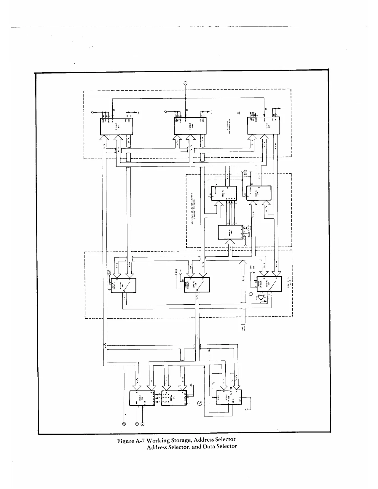
Working Storage, Address Selector and Register (Refer to Appendix A, Figure A-8) The working storage address selector and register circuitry, provide the RAM address AO-A7. These address bits locate a particular memory address to either ‘‘write’” into or ‘‘read’’ out of the RAM. This circuit is comprised of register H12, and single 4-bit register and registers J12 and I12, dual selectable 4-bit registers. Register H12, the page register, matches data bits DO-D3 to the output of H12 (QAQD). Data bits DO-D3 and the delayed data bits DO-D3 are the upper A, B, C and D inputs to devices J12 and 12. The lower A, B, C and D to J12 and 112 are the WO-W7 RAM outputs. These outputs are divided down into nibbles whereas the J12 A, B, C and D lower inputs are W4-W7 and the lower A, B, C and D inputs to R12 of W0-W3. These two quad 4-bit registers as selectable devices, therefore either the RAM output data or data register bits are selectable by the state of the select bit of pin 10, to address a given location in RAM memory.
The Data Selector (Refer to Appendix A, Figure A-8) The data selector circuitry is comprised of N11, M11 and L11 (741S157). The purpose of this circuitry is to select either the data register data bits which are at the inputs of the computational circuitry devices or the RAM output data bits which are the A input to the data selector. The outputs of L11, M11 and N11 are the register preset inputs for the program address counter.
The Computation Circuitry (Refer to Appendix A, Figure A-9) The computation circuitry is the core of the entire logic PCB. The purpose of this circuitry is to appropriately process all the information in the data instruction to the logic PCB while controlled by the sequencer logic which provides all the timing and control signals to the game logic. The ALU, a major circuitcomponent is comprised of three ALU devices N6, MG and L6. These ALU’s have the capability of
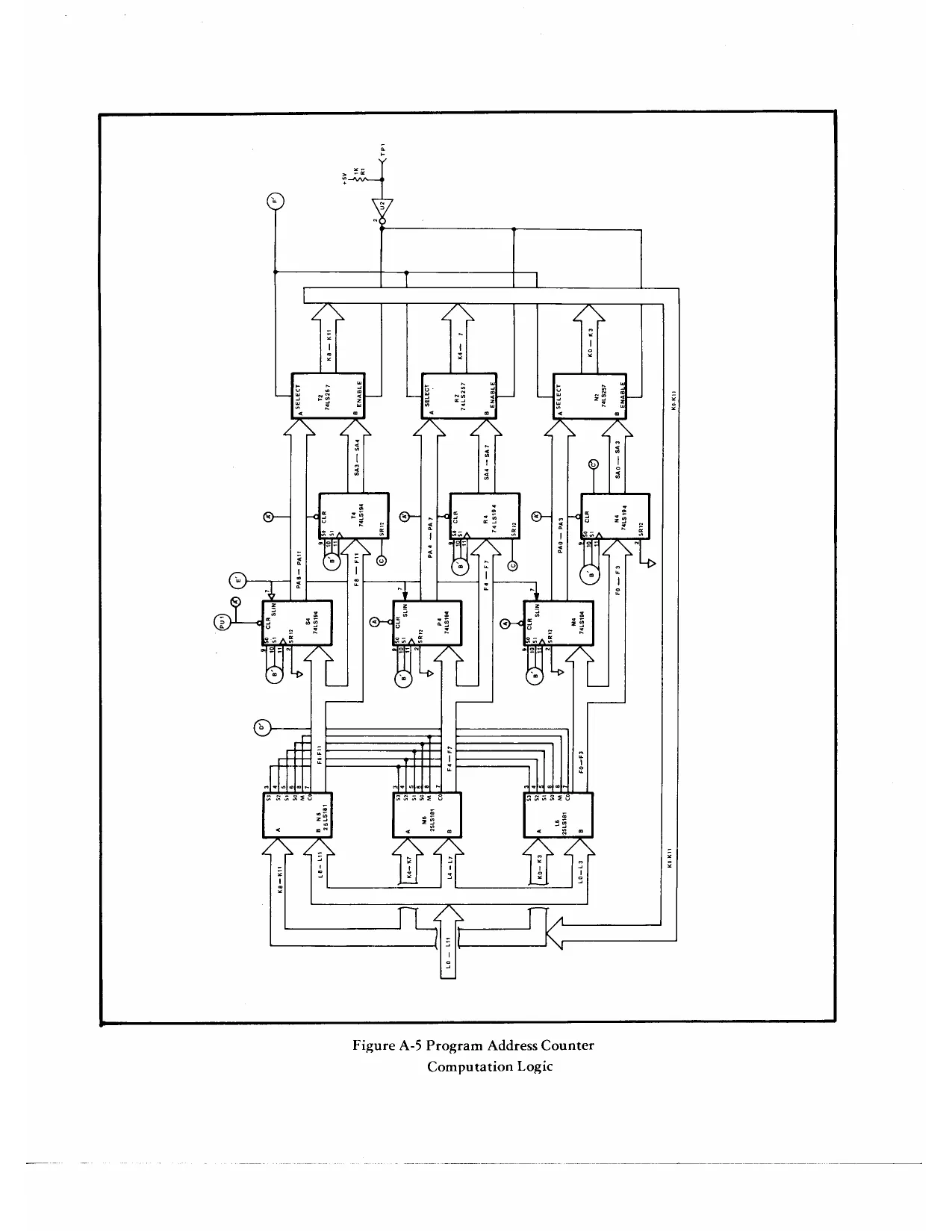
performing 16 arithmetic operations determined by inputs SO, S1, $2 and S3. These inputs re decoded by devices K2. K4 and J8. The operations process either of the A and B ALU inputs. The carry outputs (lo) are tied to look-ahead carry device L4 to be discussed later. After the operation has been performed the outputs from these ALU devices (FO-F11) are then fed to the primary and secondary accumulaters provide two function: Y and an X shift register. and arithmetic accumulators. The primary accumulator is comprised of shift registers F4, P4 and M4 (74LS194's). These shift registers ure tied together providing 12 bits of computational capability. This output addresses the ALU, the RAM and the ROM for look-up purposes. All of these outputs while in the display mode supply the X register with X data, The secondary accumulator operates very much like the primary and is
CRT NECK
MONITOR CHASSIS
Figure 4-2 CRT Magnetic Centering Rings Location comprised of shift registers T4, R4 and N4, These also cither address the program memory or provide data bits to the RAM and ALU depending on the state of the accumulator selector. The accumulator selector is comprised of data selector devices R2. N2 and T2 (7418257). This data selector selects cither input A or input B. Input A is the secondary accumulator bits SAO-SALI and input B which the primary data bits PAO PALL. These inputs are selectable by the select input line which originates from the A2 decoder (74LS107). When this bit is low it selects A input, when high it selects B input. Both select lines are commonly tied. therefore providing the identical sclect signal for N2. R2 or T2. The high speed look-ahead carey generator (7ALSIS82) together with the ALU’S provide a high speed ALU circuit
PLEXIGLASS SHIELD TENSION BOLTS
Figure 4-6 Plexiglass Shield and Plex Retainer Removal
BARRIER AUDIO BOARD ASSEMBLY
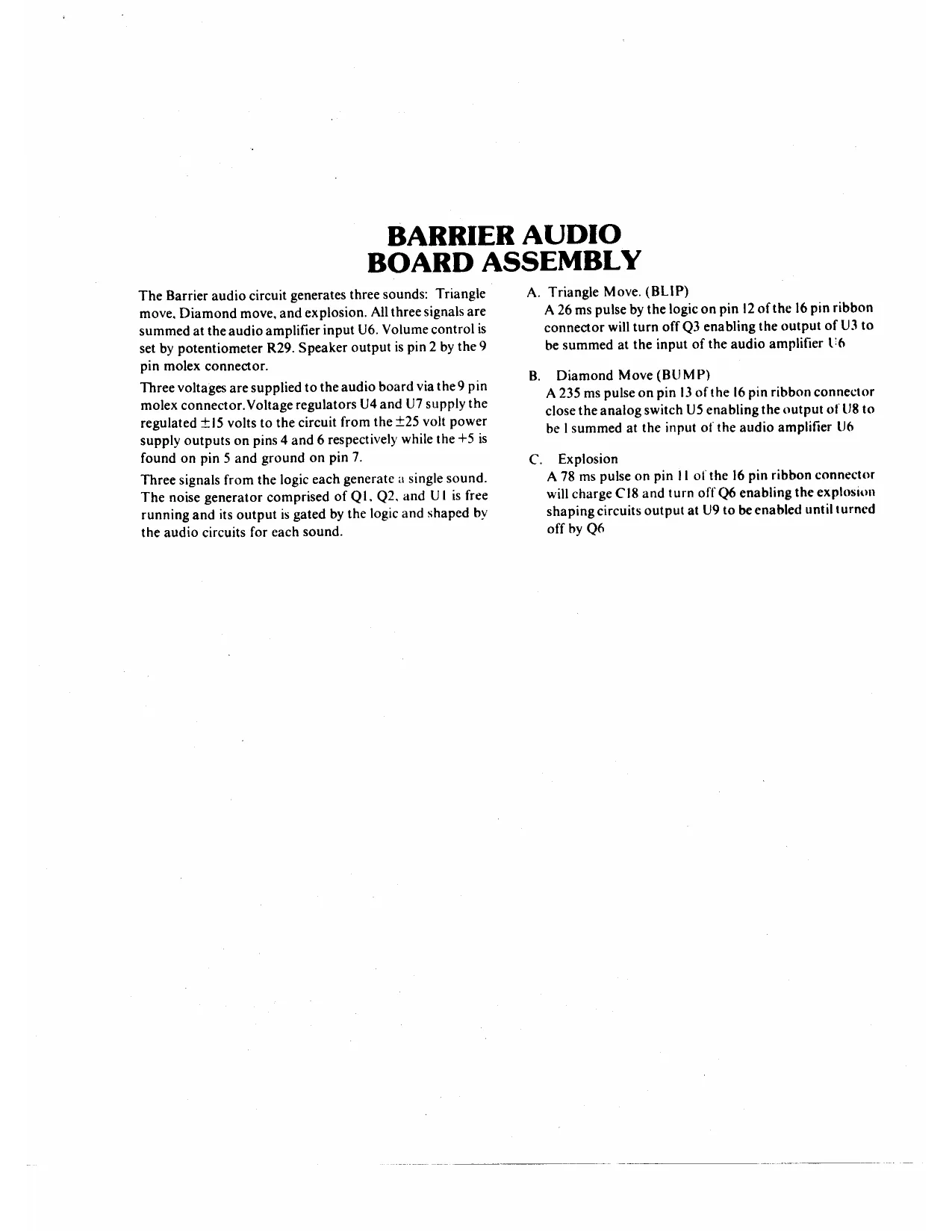
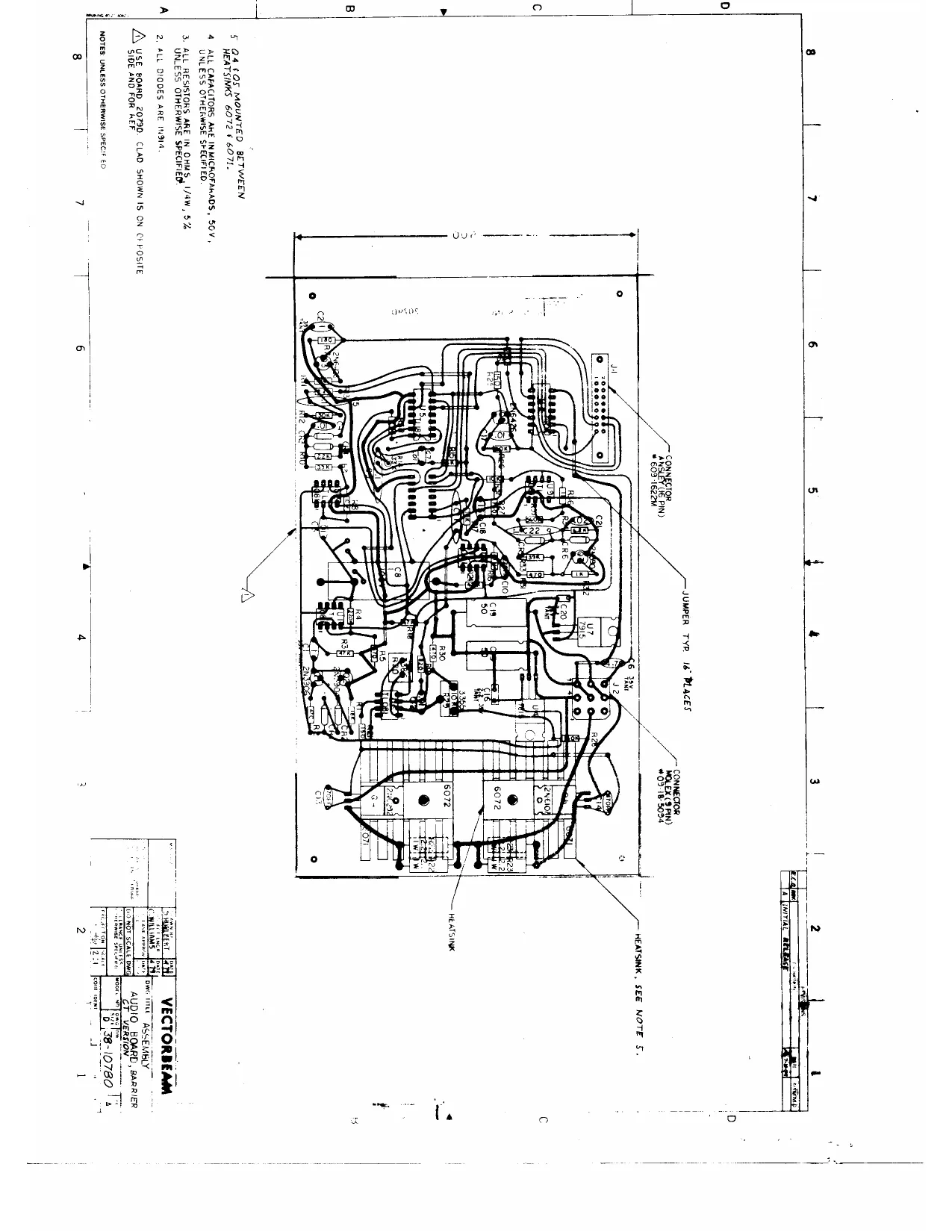
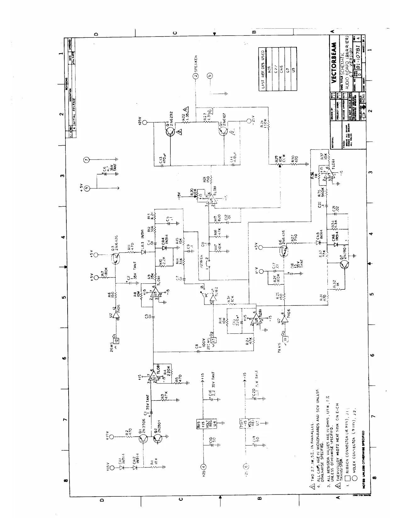
The Barrier audio circuit generates three sounds: Triangle move, Diamond move, and explosion. All three signals are summed at the audio amplifier input U6. Volume control is set by potentiometer R29. Speaker output is pin 2 by the 9 pin molex connector. Three voltages are supplied to the audio board via the9 pin molex connector. Voltage regulators U4 and U7 supply the regulated +15 volts to the circuit from the +25 volt power supply outputs on pins 4 and 6 respectively while the +5 is found on pin 5 and ground on pin 7. Three signals from the logic each generate « single sound. The noise generator comprised of Q1, Q2. and UL is free running and its output is gated by the logic and shaped by the audio circuits for each sound. A. Triangle Move. (BLIP) A 26 ms pulse by the logic on pin 12 of the 16 pin ribbon connector will turn off Q3 enabling the output of U3 to be summed at the input of the audio amplifier U6
B. Diamond Move (BUMP) A 235 ms pulse on pin 13 of the 16 pin ribbon connector close the analog switch US enabling the output of U8 to be | summed at the input of the audio amplifier U6
Cc. Explosion A 78 ms pulse on pin I of the 16 pin ribbon connector will charge C18 and turn off Q6 enabling the explosion shaping circuits output at U9 to be enabled until turned off by Q6
This page is a drawing, shown as the original scan.
This page is a drawing, shown as the original scan.
This page is a drawing, shown as the original scan.
This page is a drawing, shown as the original scan.
This page is a drawing, shown as the original scan.
This page is a drawing, shown as the original scan.
This page is a drawing, shown as the original scan.
This page is a drawing, shown as the original scan.
This page is a drawing, shown as the original scan.
This page is a drawing, shown as the original scan.
This page is a drawing, shown as the original scan.
This page is a drawing, shown as the original scan.
This page is a drawing, shown as the original scan.
This page is a drawing, shown as the original scan.
This page is a drawing, shown as the original scan.
This page is a drawing, shown as the original scan.
This page is a drawing, shown as the original scan.