Pole Position SP-218 8th Printing
Pole Position (World) (Namco, 1982) · Schematic Package · 32 pages · 26 sections · original scan
Sheet 1A
Sheet 1B
Sheet 2A
Sheet 2B
Sheet 3A
Sheet 3B
Sheet 4A
Sheet 4B Sheet 5A Sheet 5B Sheet 6A Sheet 6B Sheet 7A Sheet 7B Sheet 8A Sheet 8B Sheet 9A Sheet 9B Sheet 10A
Sheet 10B Sheet 11A Sheet 11B
Sheet 12A Sheet 12B Sheet 13A Sheet 13B Sheet 14A Sheet 14B Sheet 154 Sheet 15B
Sheet 16A
Sheet 16B Table of Contents
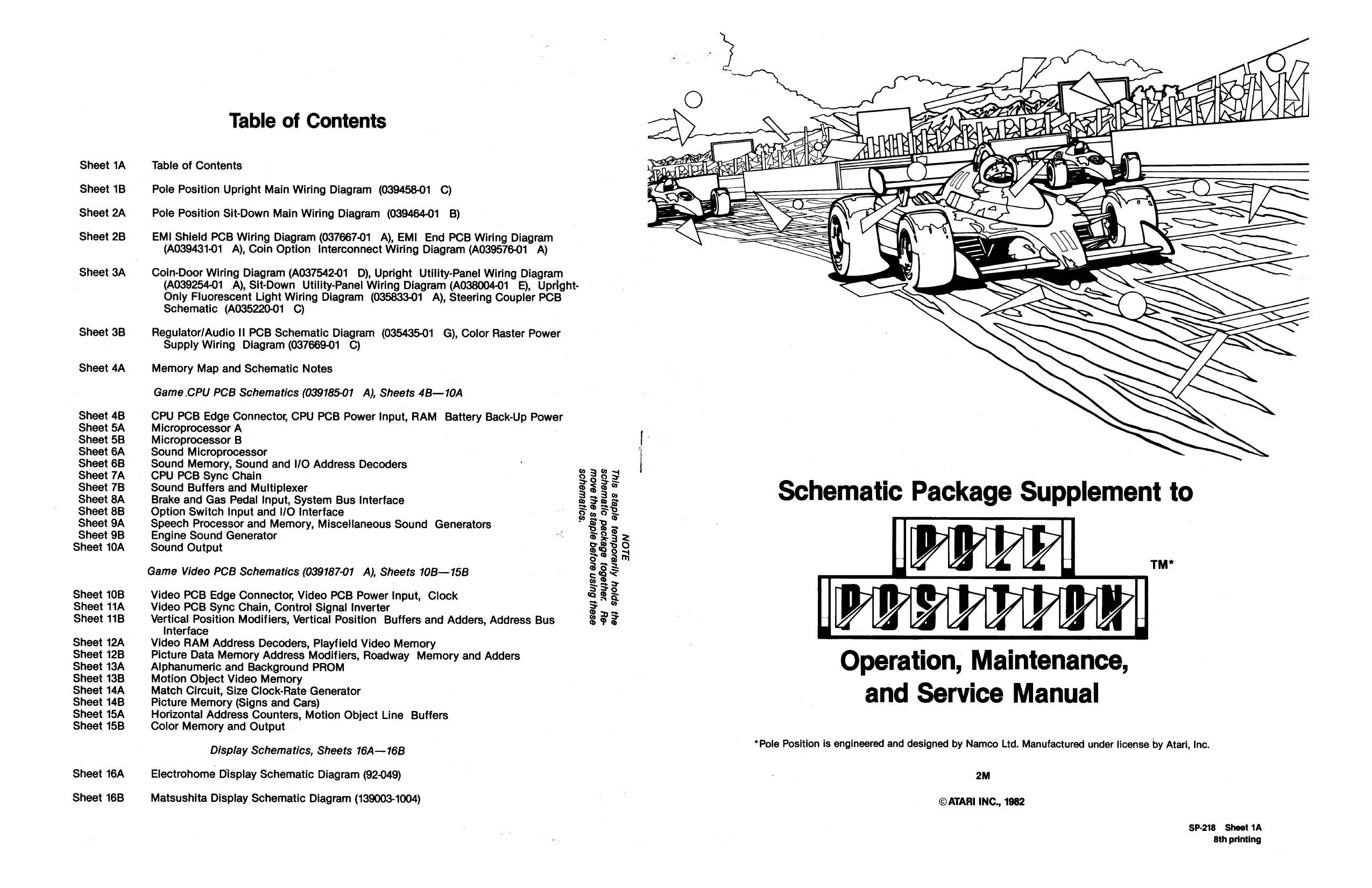
Table of Contents
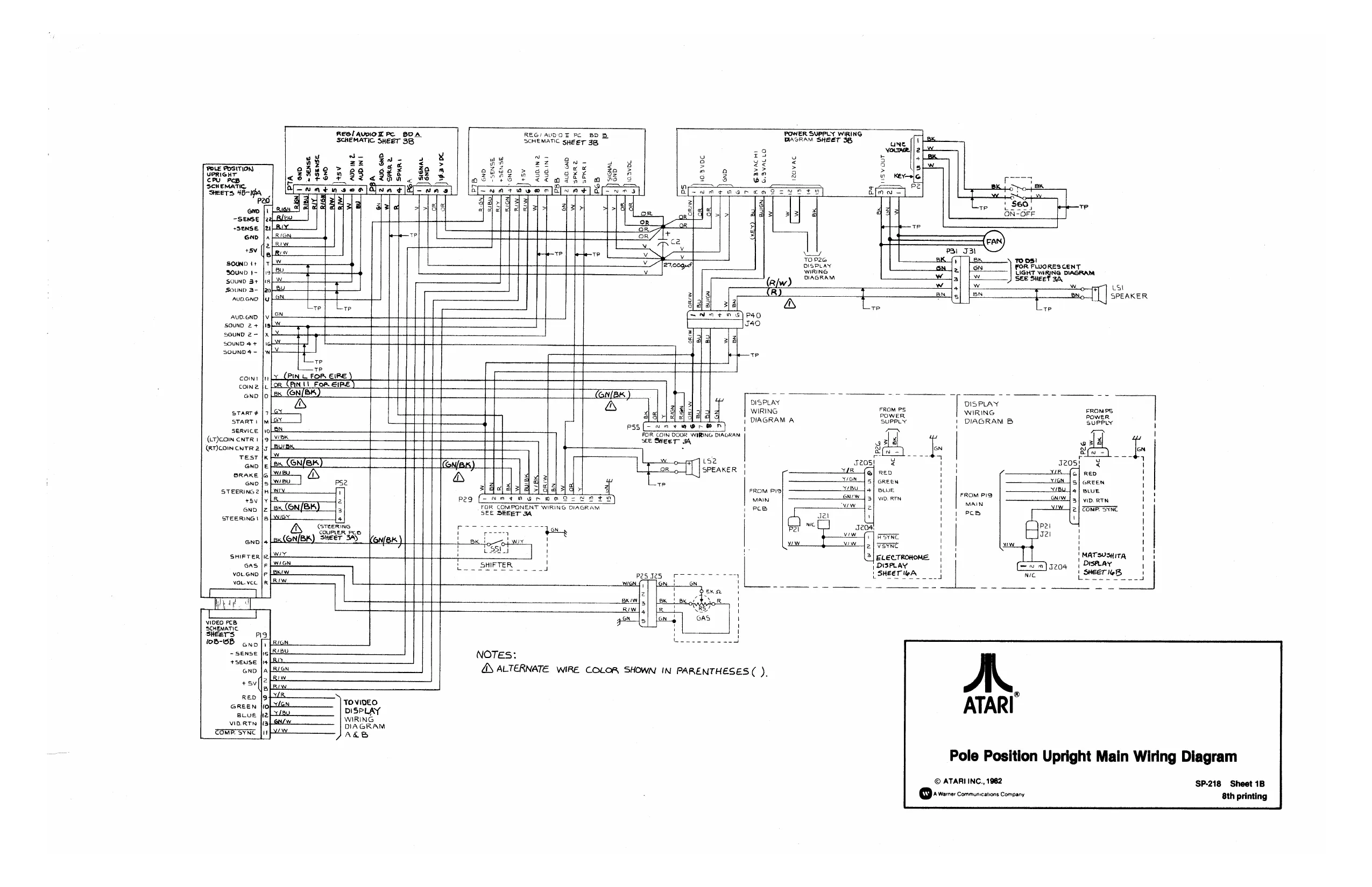
Pole Position Upright Main Wiring Diagram (039458-01 C)
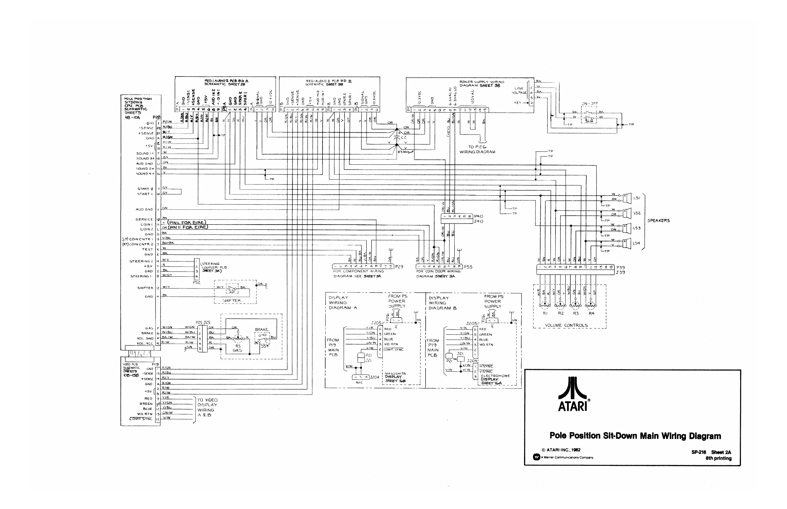
Pole Position Sit-Down Main Wiring Diagram (039464-01 B)
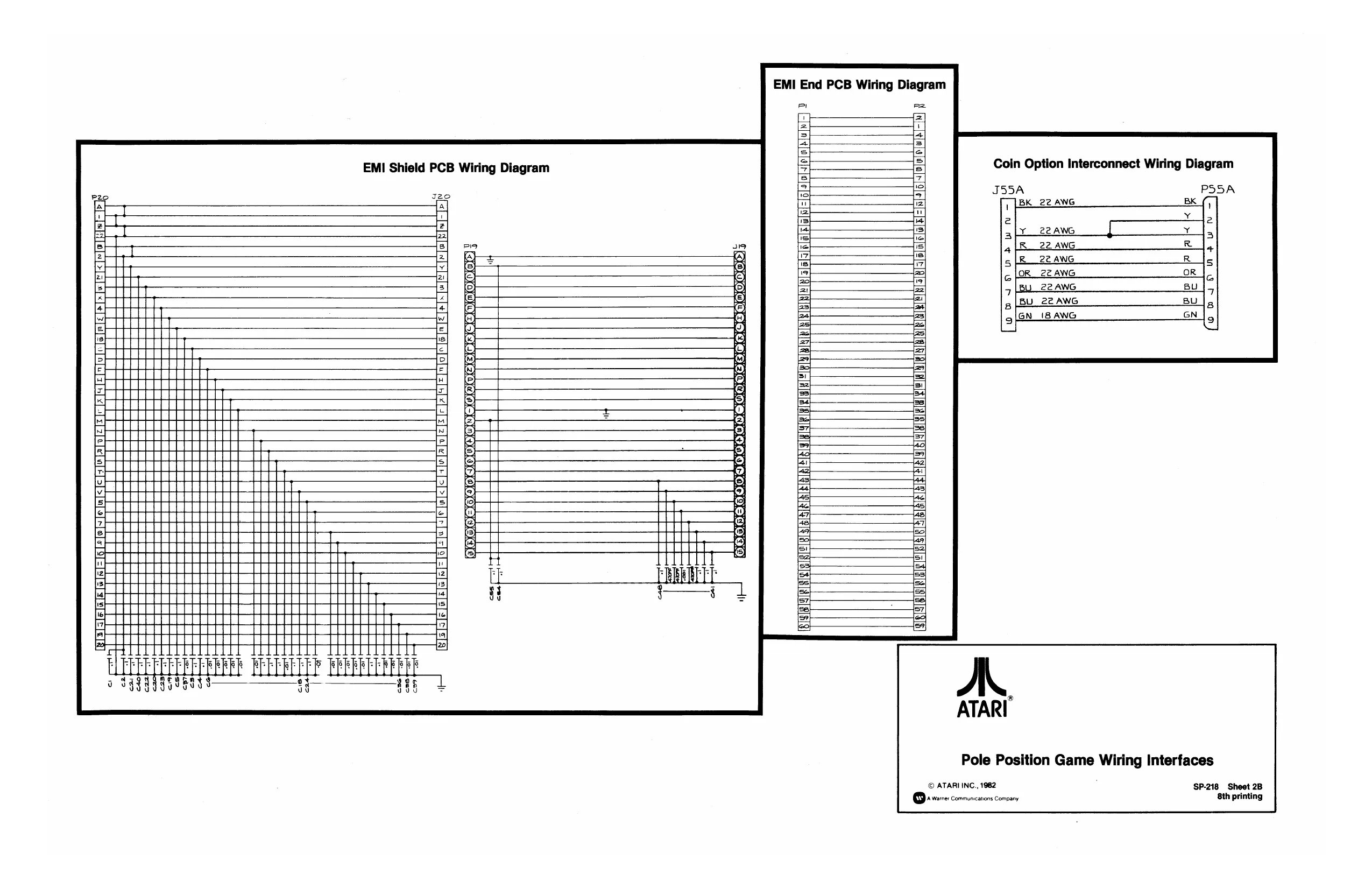
EMI Shield PCB Wiring Diagram (037667-01 A), EMI End PCB Wiring Diagram (A039431-01 A), Coin Option Interconnect Wiring Diagram (A039576-01 A)
Coin-Door Wiring Diagram (A037542-01 D), Upright Utility-Panel Wiring Diagram (A039254-01 .A), Sit-Down Utility-Panel Wiring Diagram (A038004-01 £), Upright- Only Fluorescent Light Wiring Diagram (035833-01 A), Steering Coupler PCB Schematic (A035220-01 C)
Regulator/Audio Il PCB Schematic Diagram (035435-01 G), Color Raster Power Supply Wiring Diagram (037669-01 C)
Memory Map and Schematic Notes
Game .CPU PCB Schematics (039185-01 A), Sheets 4B—10A
CPU PCB Edge Connector, CPU PCB Power Input, RAM Battery Back-Up Power Microprocessor A Microprocessor B Sound Microprocessor Sound Memory, Sound and I/O Address Decoders CPU PCB Sync Chain Sound Buffers and Multiplexer Brake and Gas Pedal Input, System Bus Interface Option Switch Input and I/O Interface Speech Processor and Memory, Miscellaneous Sound Generators Engine Sound Generator Sound Output
Game Video PCB Schematics (039187-01 A), Sheets 10B—15B
Video PCB Edge Connector, Video PCB Power Input, Clock Video PCB Sync Chain, Control Signal Inverter Vertical Position Modifiers, Vertical Position Buffers and Adders, Address Bus Interface Video RAM Address Decoders, Playfield Video Memory Picture Data Memory Address Modifiers, Roadway Memory and Adders Alphanumeric and Background PROM Motion Object Video Memory Match Circuit, Size Clock-Rate Generator Picture Memory (Signs and Cars) Horizontal Address Counters, Motion Object Line Buffers Color Memory and Output
Display Schematics, Sheets 16A—16B
Electrohome Display Schematic Diagram (92-049)
Matsushita Display Schematic Diagram (139003-1004) "soyjBWeyos esey) Bujsn asojeq ajde}s ay} eAOW -0y 1843960) abeyord oeweyos ey} spjoy Ajjsesodwea} ajdejs siyy O
Bs dK
FLON TM*
Operation, Maintenance, and Service Manual
*Pole Position is engineered and designed by Namco Ltd. Manufactured under license by Atari, Inc.
2M
©ATARI INC., 1982
SP-218 Sheet 1A 8th printing
This page is a drawing, shown as the original scan.
This page is a drawing, shown as the original scan.
This page is a drawing, shown as the original scan.
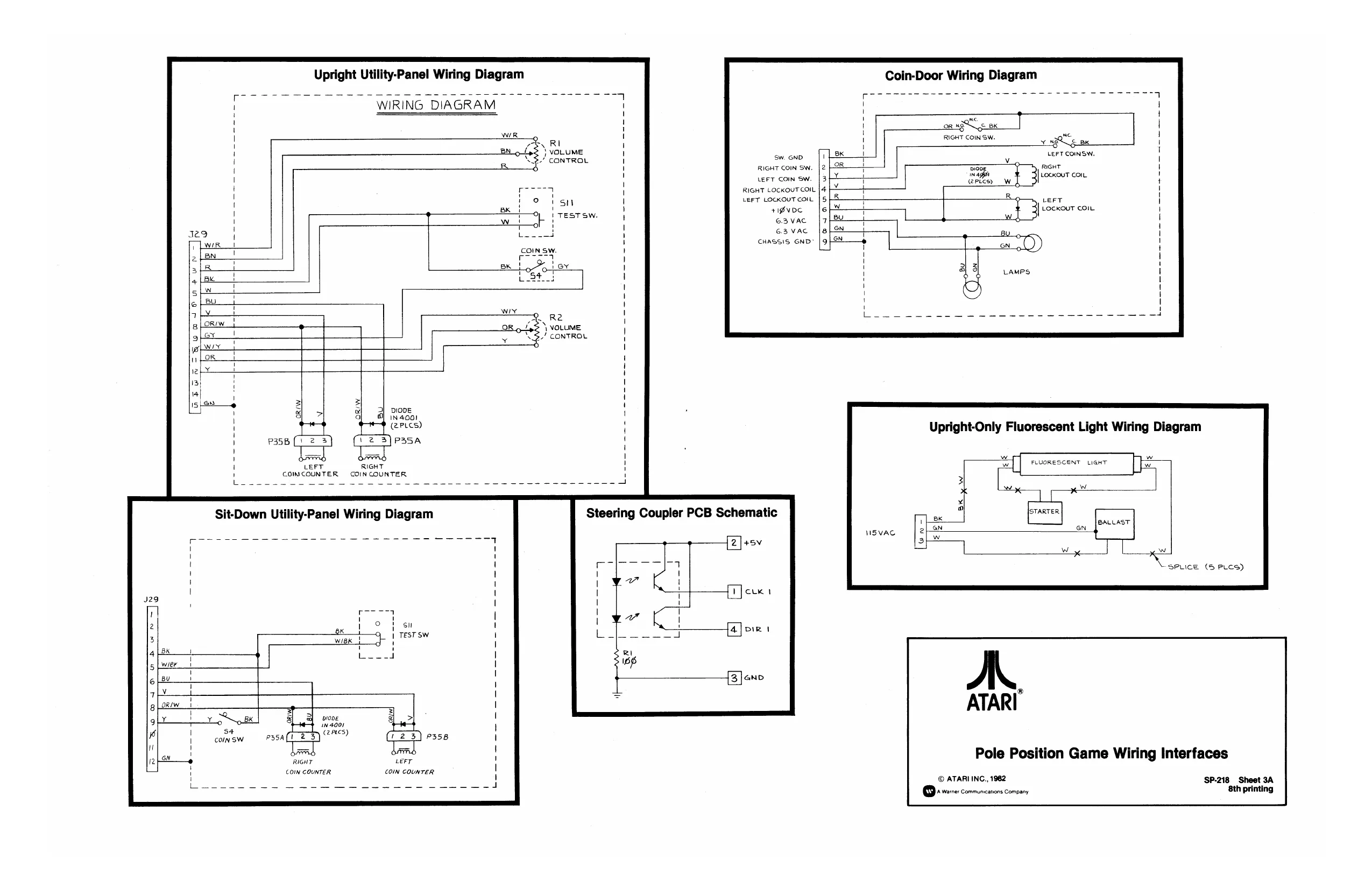
This page is a drawing, shown as the original scan.
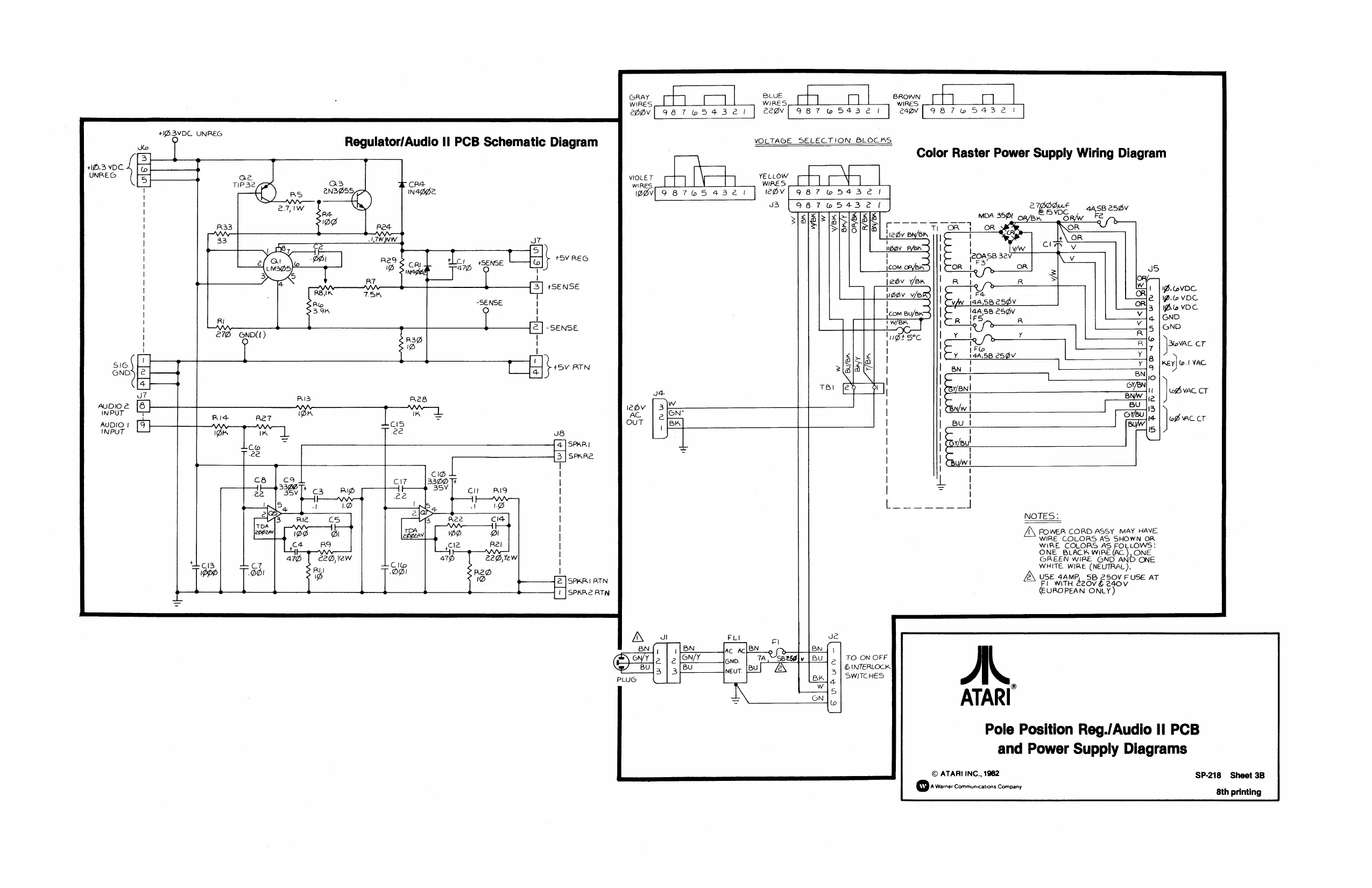
This page is a drawing, shown as the original scan.
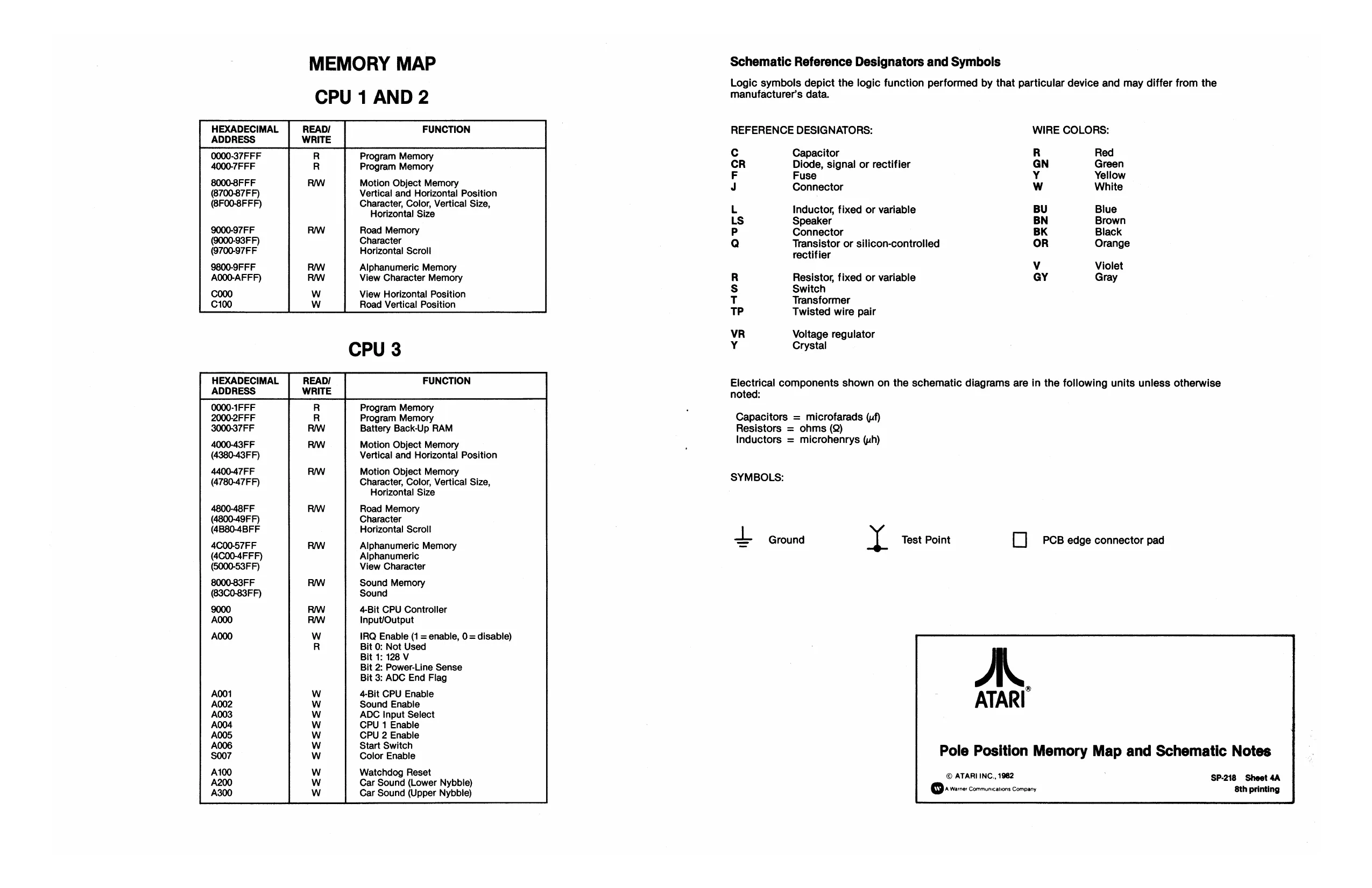
MEMORY MAP Schematic Reference Designators and Symbols Logic symbols depict the logic function performed by that particular device and may differ from the CPU 1 AND 2 manufacturer's data.
HEXADECIMAL FUNCTION REFERENCE DESIGNATORS: WIRE COLORS:
ADDRESS
(0000-37FFF Program Memory c Capacitor R Red
4000-7FFF Program Memory ie Diode; signal or rectifier on een
use fellow
8000-8FFF Motion Object Memory r
(8700-87FF) Vertical and Horizontal Positi J Connector Me White
| BFORSEFP) | Character Cor Veruca) Size, | L | Inductor, fixed or variable | BU | Blue |
Ls Speaker BN Brown
| peseaiae | pe Moran | P | Connector | BK | Black |
(9000-§ acter ili -¢
| (@70097FF | Horizontal Scroll | Q | adr or silicon-controlled | OR | Orange |
| 9800-9FFF | Alphanumeric Memory | v | Violet | ||
| A000-AFFF) | View Character Memory | R | Resistor, fixed or variable | GY | Gray |
| 5 | 5 | =" | Ss | Switch |
C000 View Horizontal Position
| C100 | Road Vertical Position | ul | ene tornelaas |
™ Twisted wire pair
VR Voltage regulator Y Crystal CPU 3
| HEXADECIMAL | READ/ | FUNCTION | Electrical components shown on the schematic diagrams are in the following units unless otherwise |
| ADDRESS | WRITE | noted: | |
| 0000-1FFF | R | Program Memory | . |
| 2000-2FFF | R | Program Memory | Capacitors = microfarads (uf) |
| 3000-37FF | Battery Back-Up RAM | Resistors = ohms (Q) | |
| 4000-43FF | Motion Object Memory | Inductors = microhenrys (uh) |
(4380-43FF) Vertical and Horizontal Position 4400-47FF Motion Object Memory .
| (4780-47FF) | Character, Color, Vertical Size, | SYMBOLS: |
Horizontal Size 4800-48FF Road Memory (4800-49FF) Character
| (4B80-4BFF | Horizontal Scroll | Lt | . | |||
| 4C00-57FF | Alphanumeric Memory | — | Ground | Test Point | Oo | PCB edge connector pad |
(4C00-4FFF) Alphanumeric (6000-53FF) View Character 8000-83FF Sound Memory (83C0-83FF) Sound 9000 4-Bit CPU Controller A000 Input/Output A000 IRQ Enable (1 = enable, 0 = disable) Bit 0: Not Used Bit 1: 128 V Bit 2: Power-Line Sense Bit 3: ADC End Flag " ®
| A001 | w | 4-Bit CPU Enable | ||||
| A002 | Ww | Sound Enable | ATARI | |||
| A003 | Ww | ADC Input Select | ||||
| A004 | Ww | CPU 1 Enable | ||||
| A005, | Ww | CPU 2 Enable | ||||
| A006 | Ww | Start Switch | ||||
| S007 | w | Color Enable | Pole Position Memory Map and Schematic Notes | |||
| A100 | Ww | Watchdog Reset | © ATARIINC., 1982 | |||
| A200 | Ww | Car Sound (Lower Nybble) | o ©! A 7 HINC., | 1! | ; | sae eneet 4 |
| A300 | Ww | Car Sound (Upper Nybble) | aroer Communications Company | Printing |
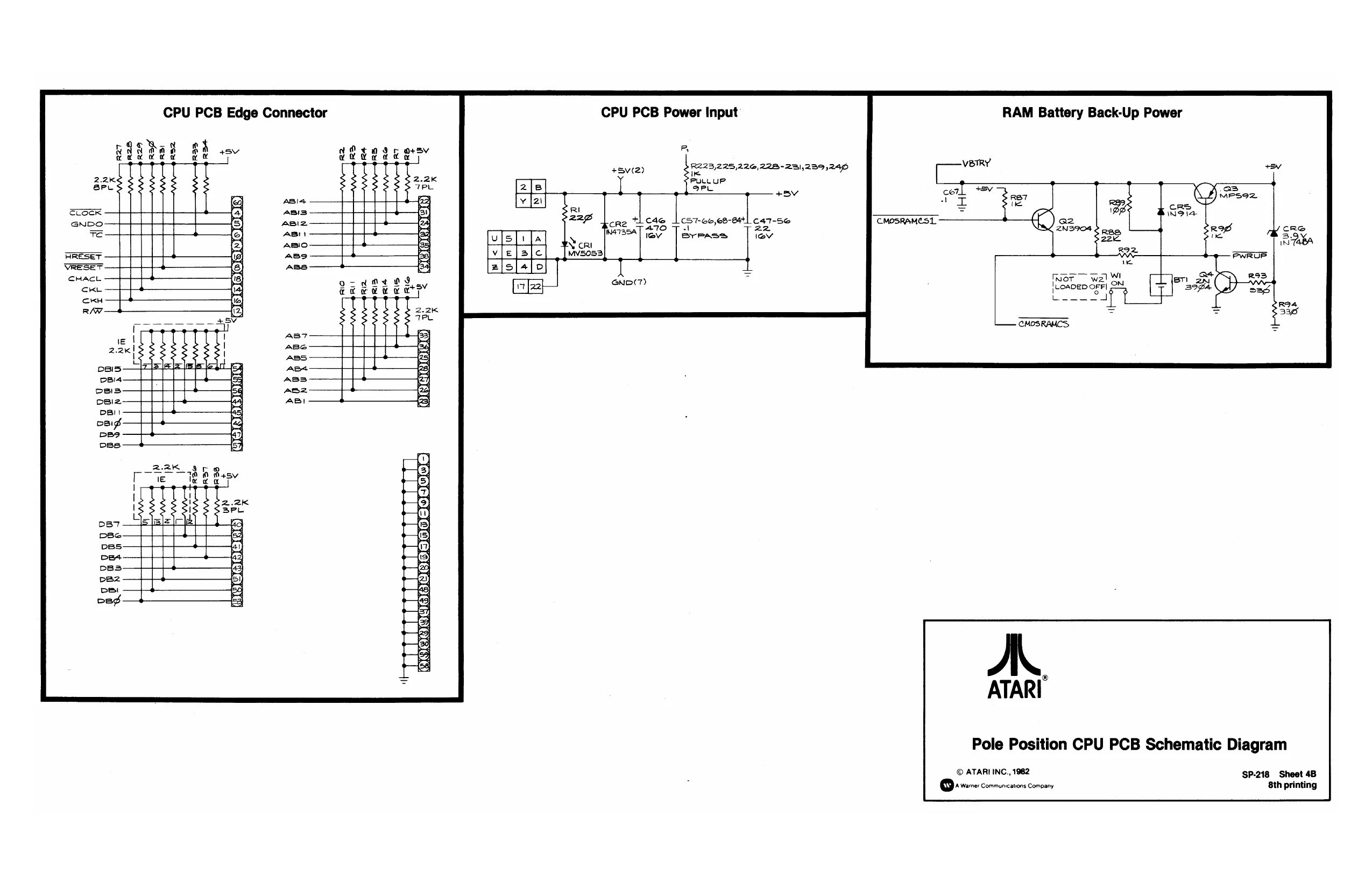
This page is a drawing, shown as the original scan.
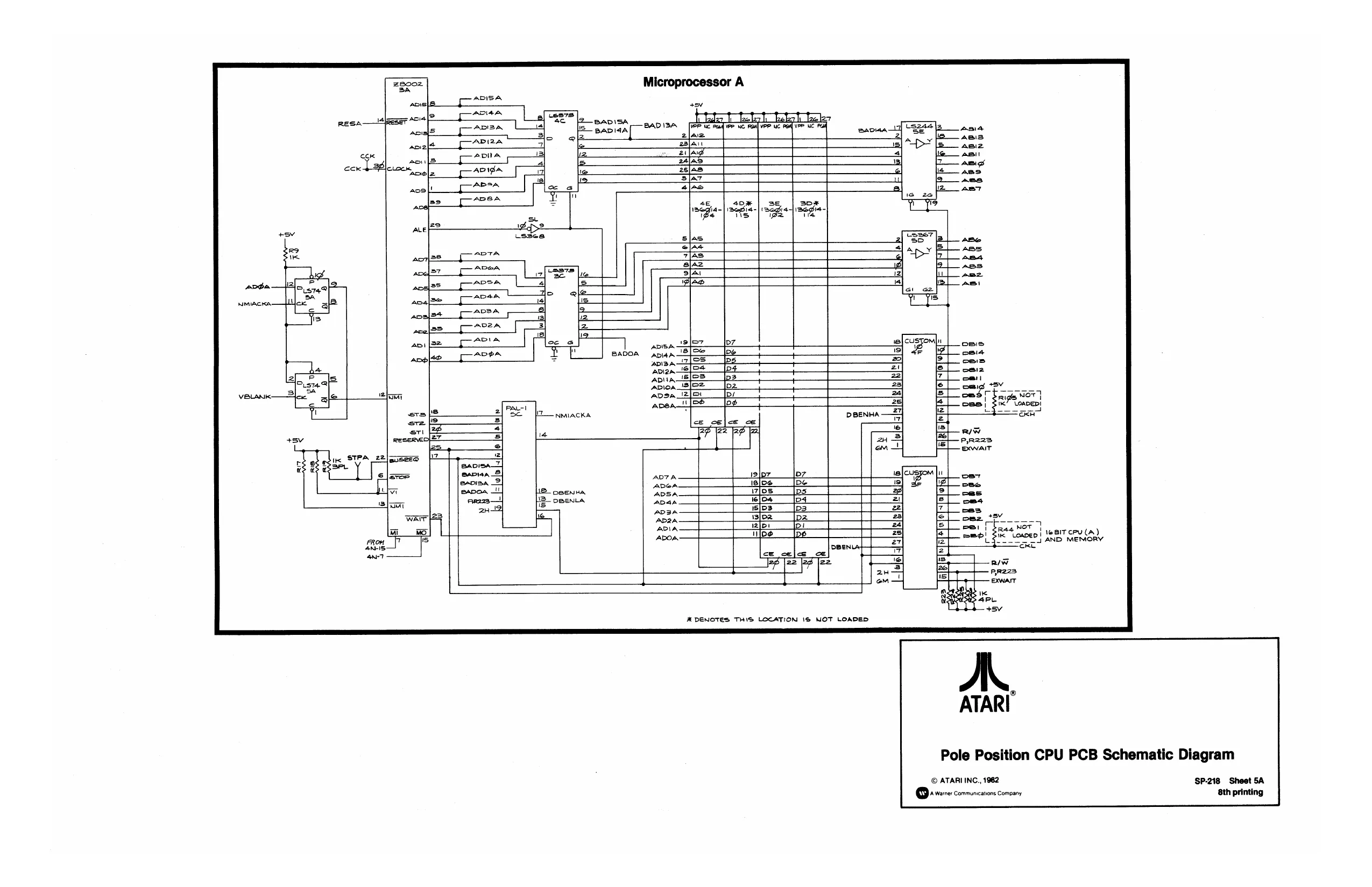
This page is a drawing, shown as the original scan.
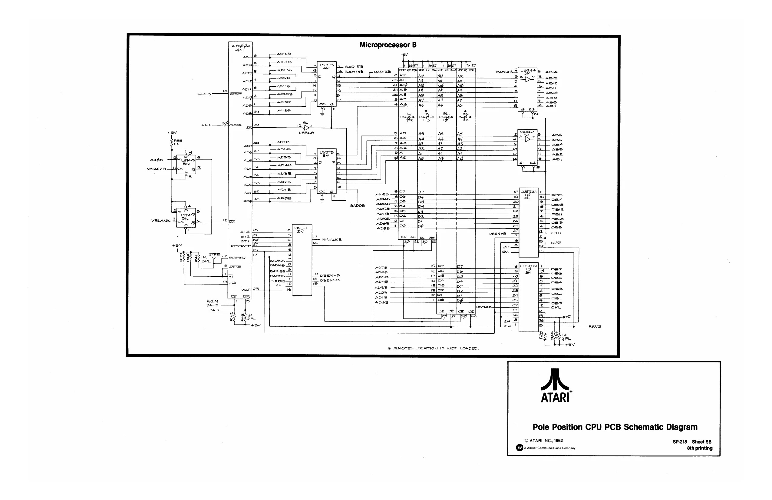
This page is a drawing, shown as the original scan.
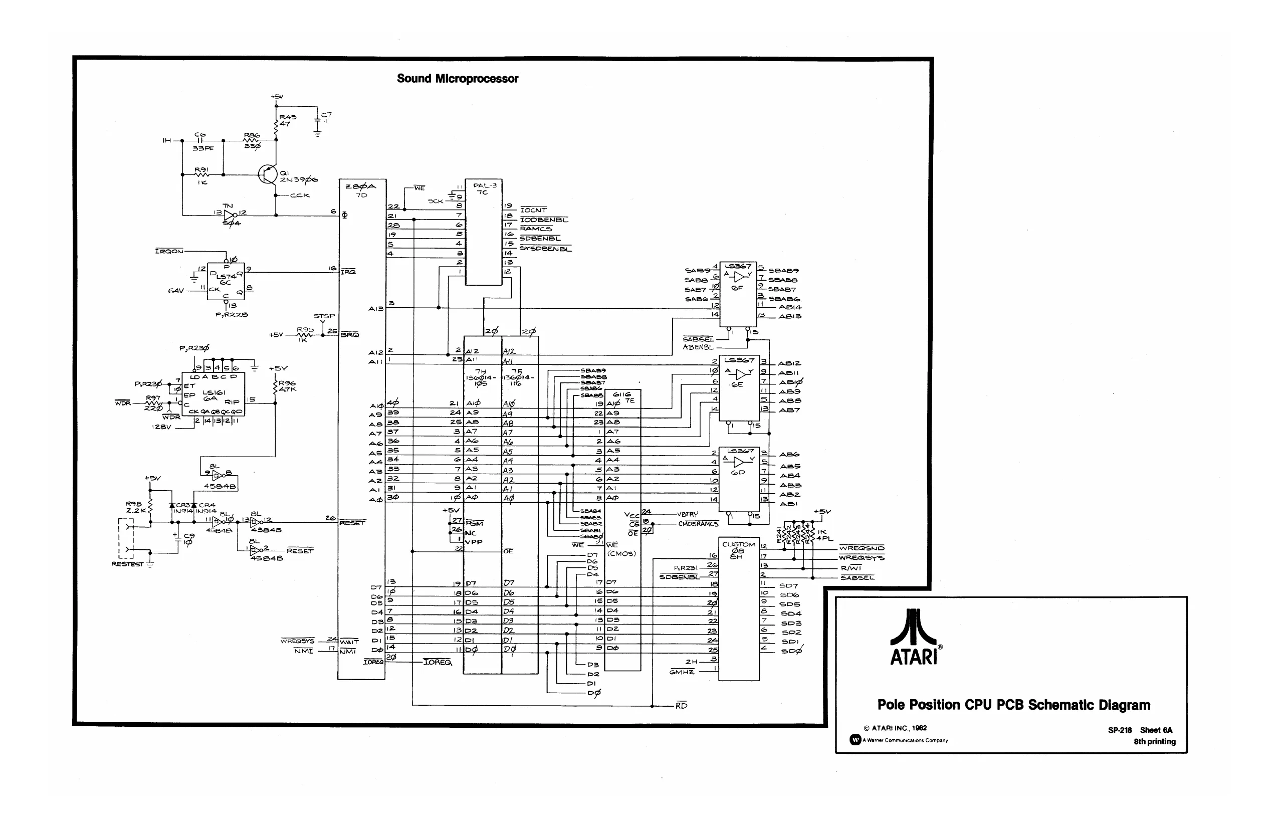
This page is a drawing, shown as the original scan.
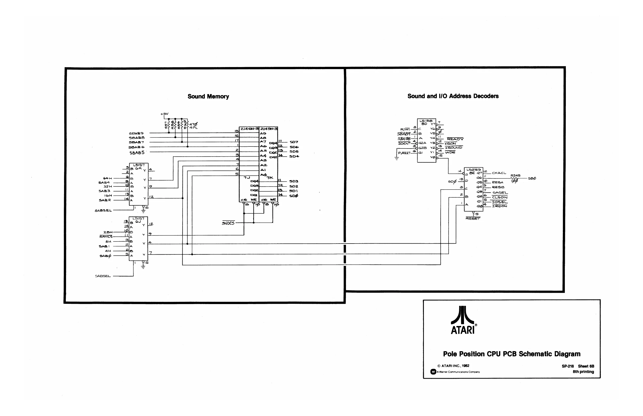
This page is a drawing, shown as the original scan.
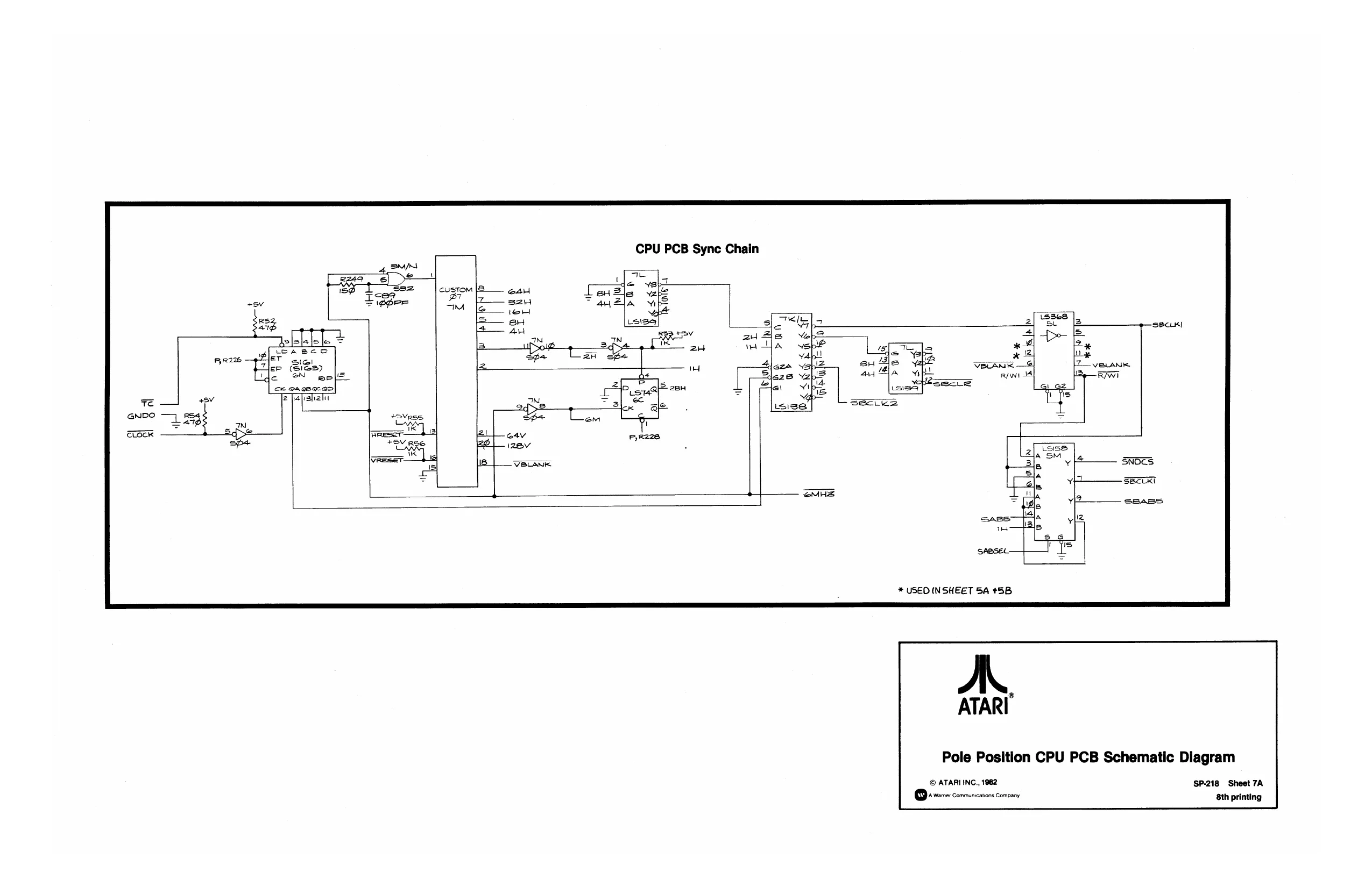
This page is a drawing, shown as the original scan.
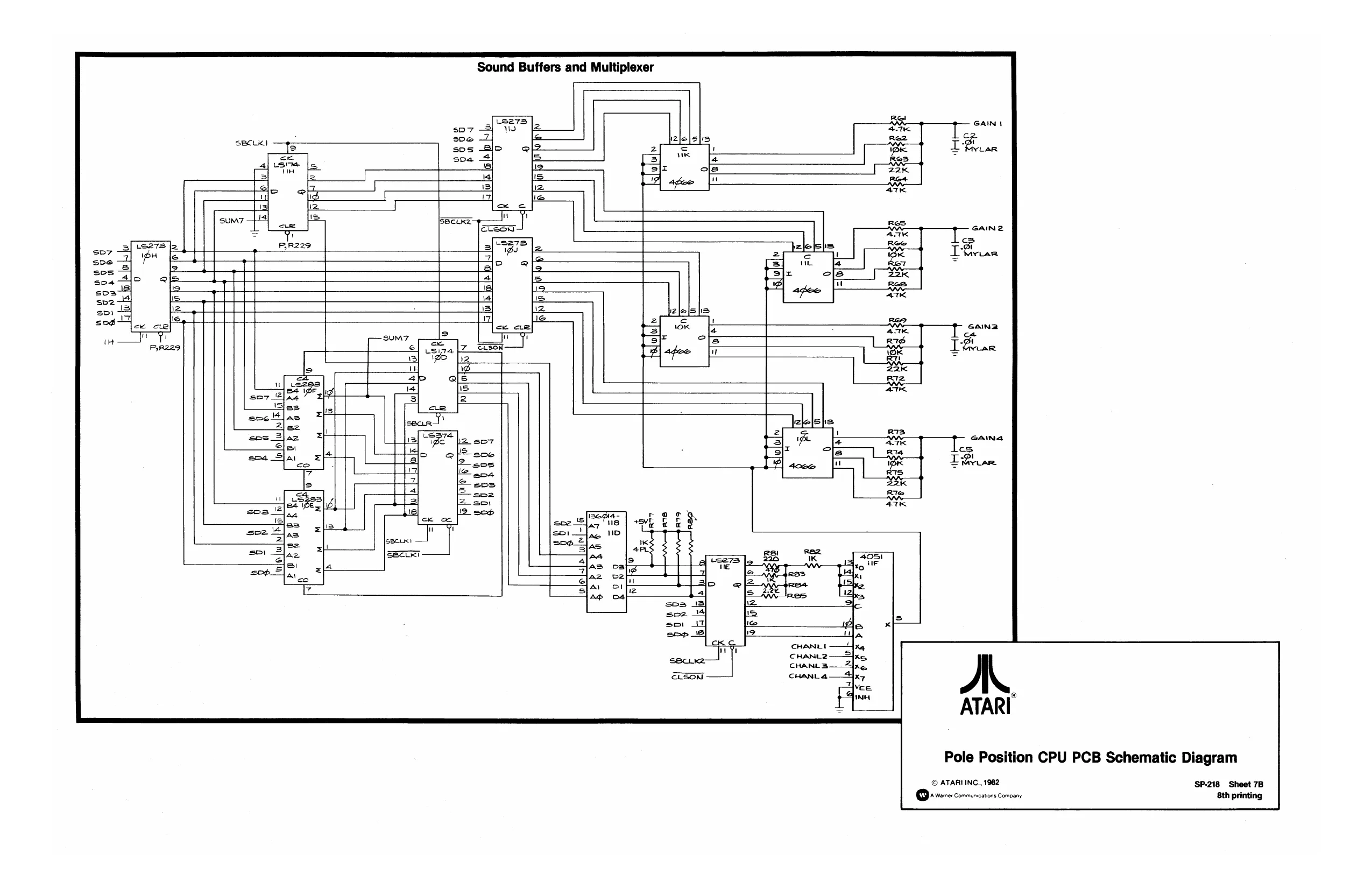
This page is a drawing, shown as the original scan.
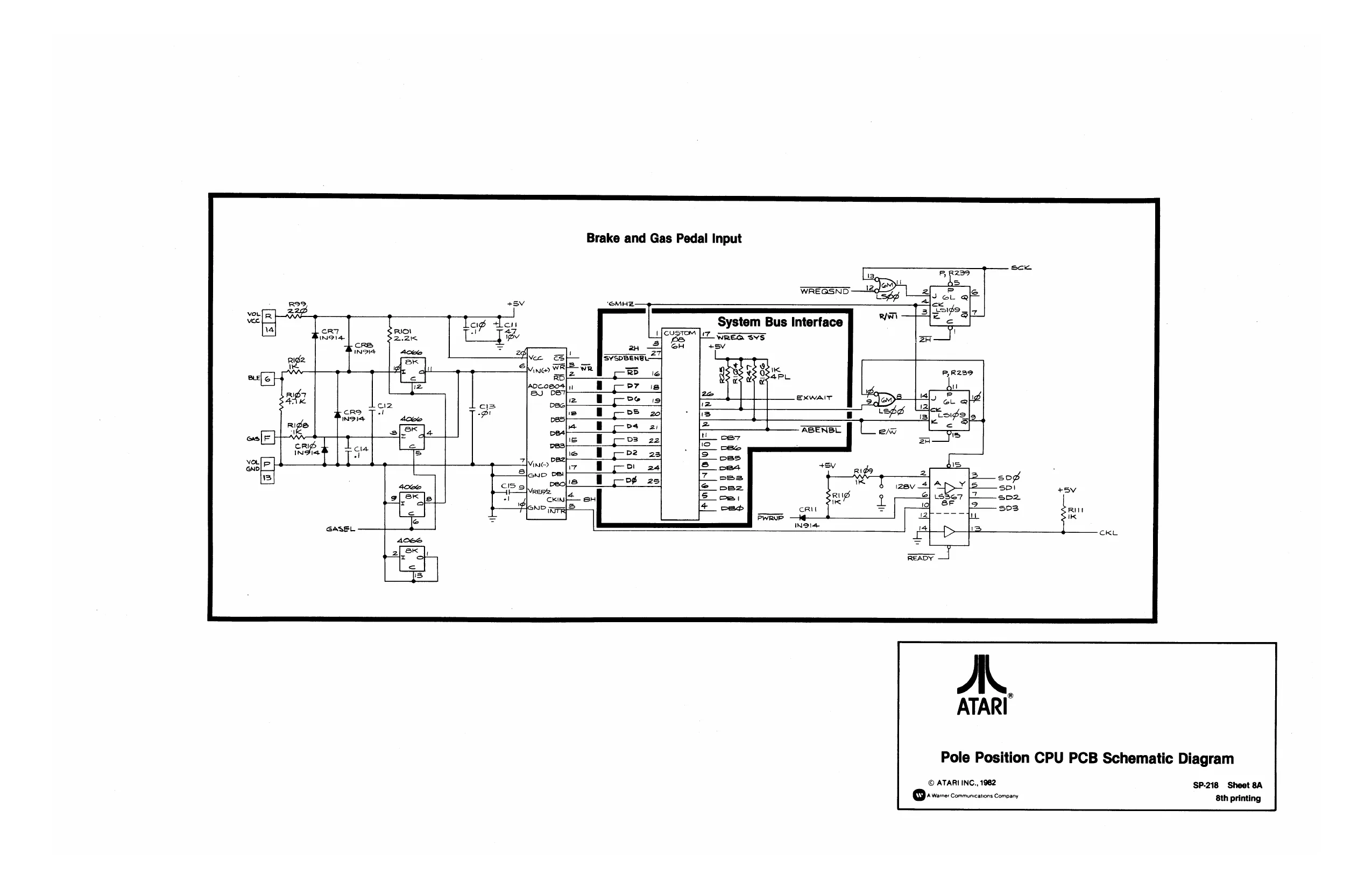
This page is a drawing, shown as the original scan.
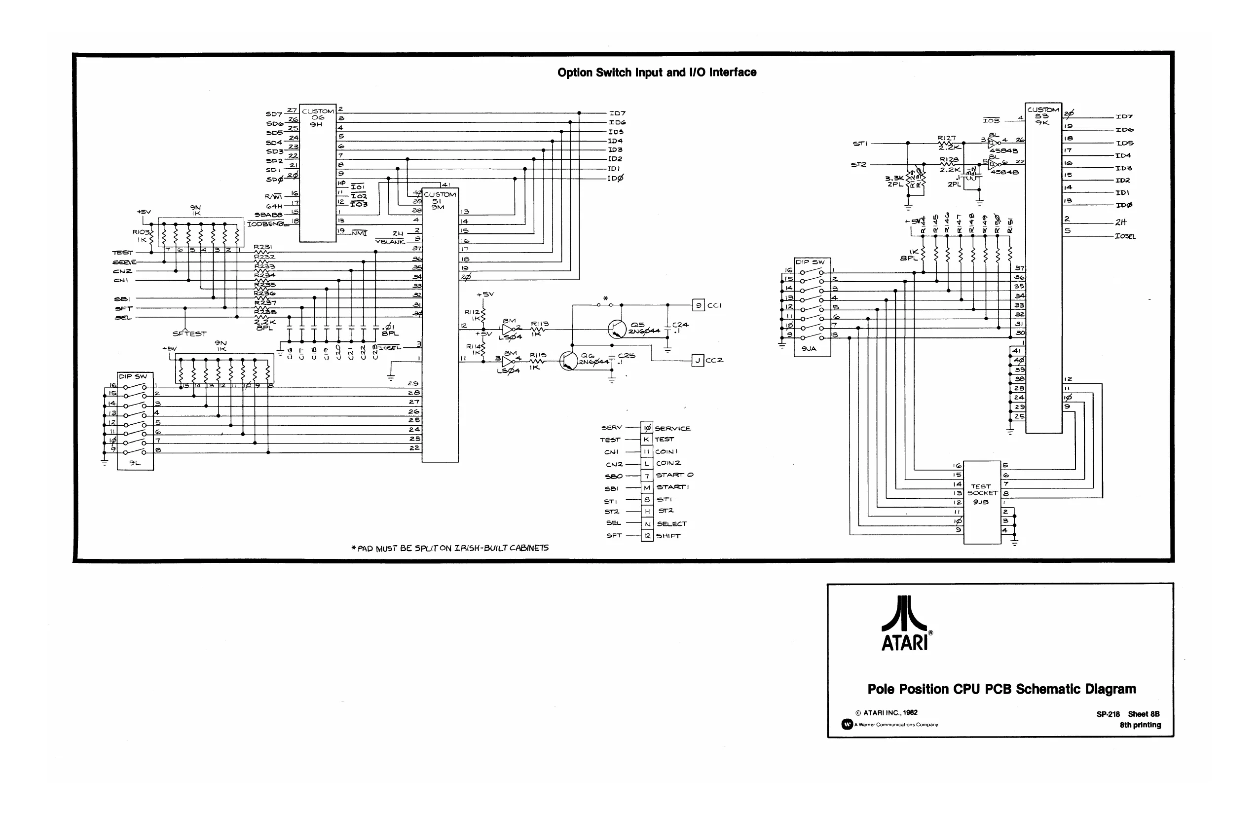
This page is a drawing, shown as the original scan.
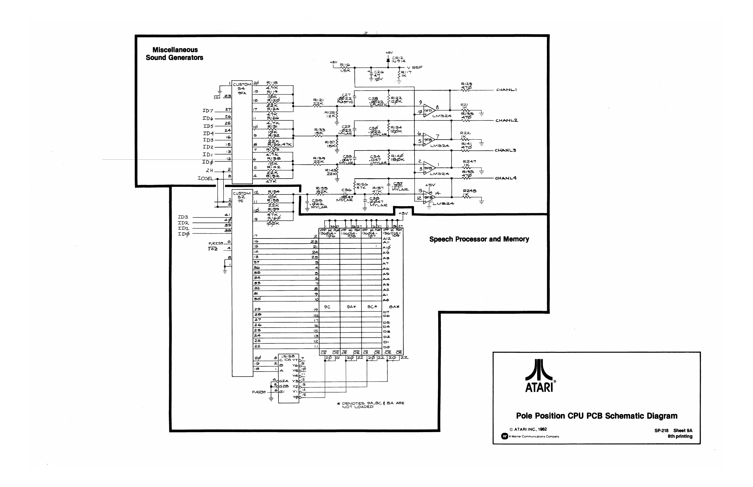
This page is a drawing, shown as the original scan.
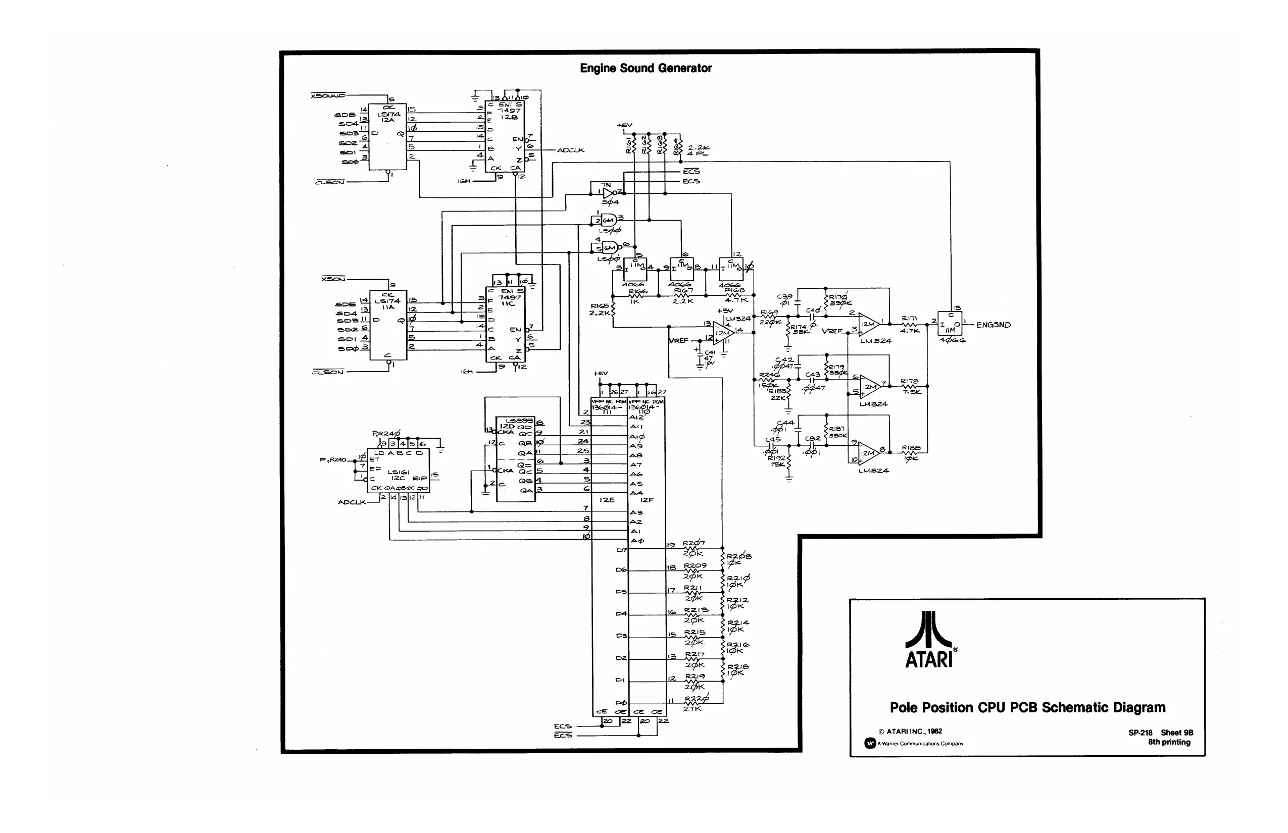
This page is a drawing, shown as the original scan.
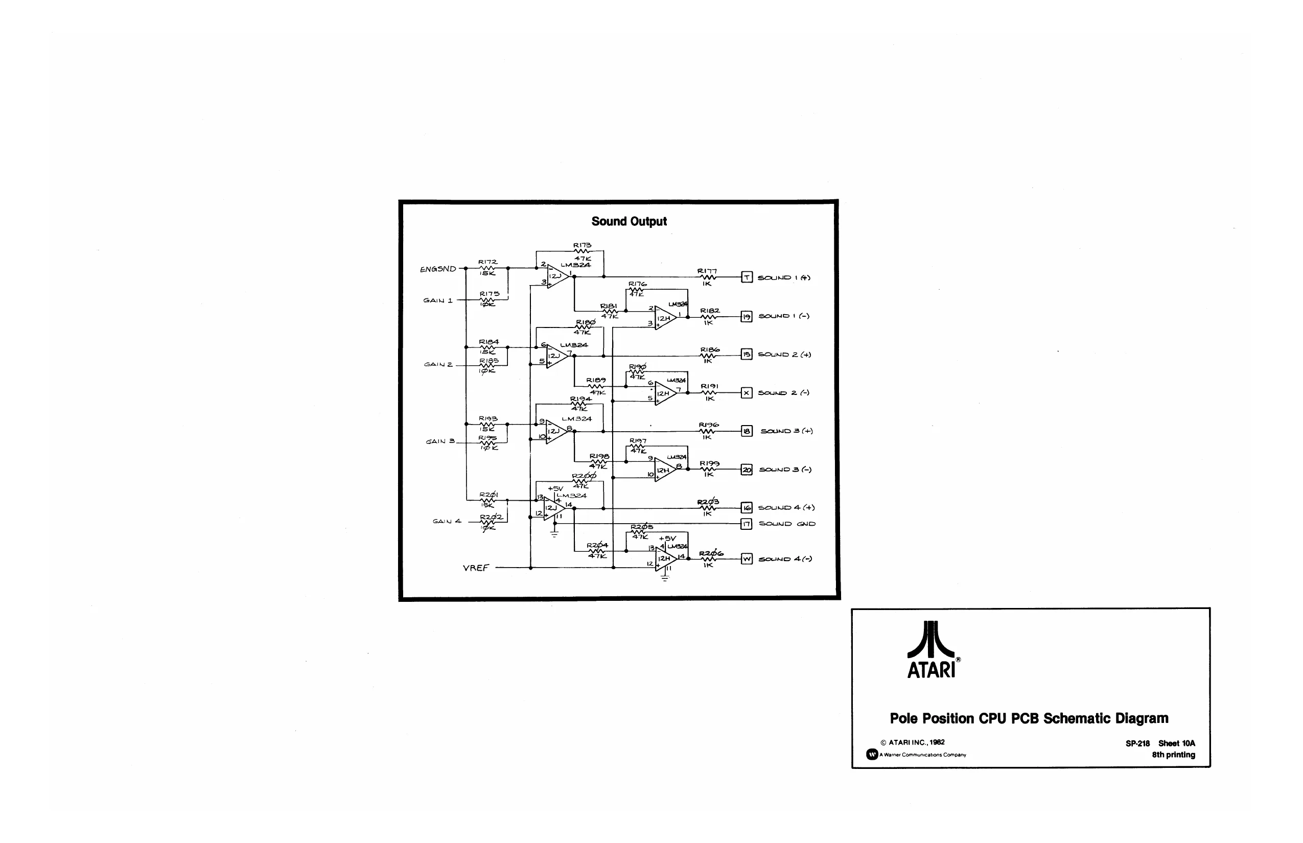
This page is a drawing, shown as the original scan.
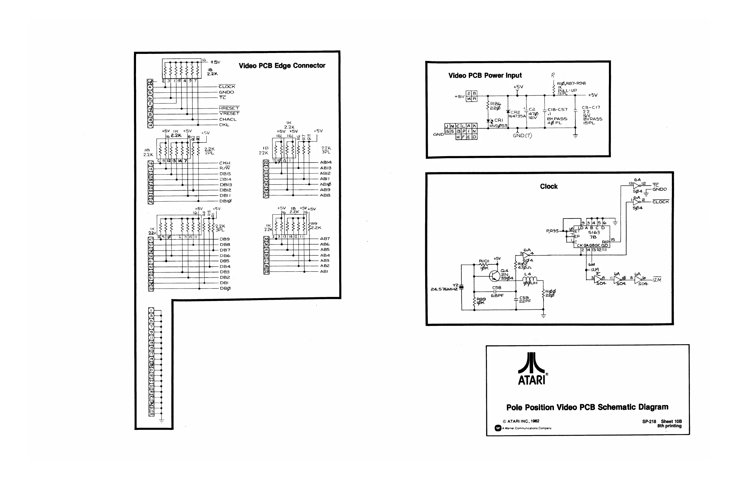
This page is a drawing, shown as the original scan.
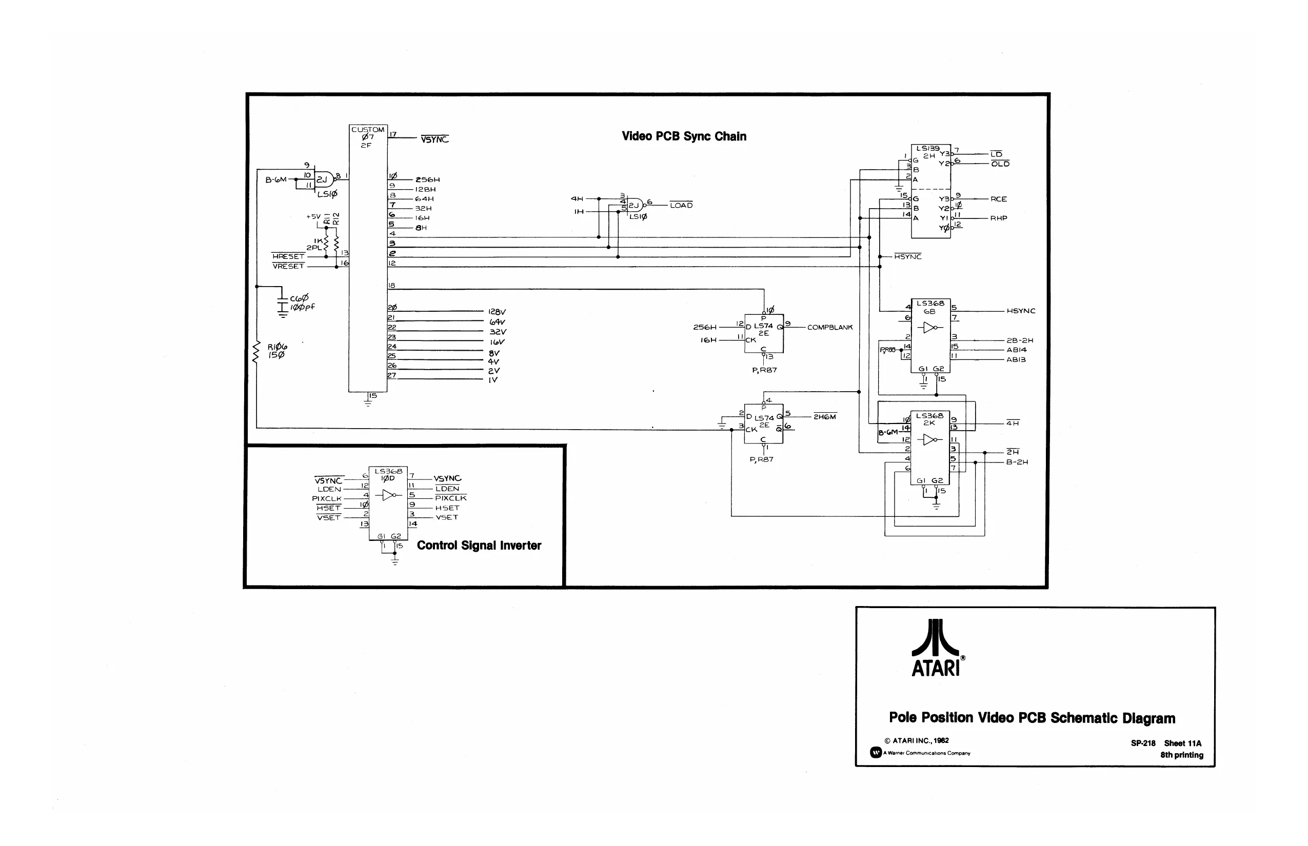
This page is a drawing, shown as the original scan.
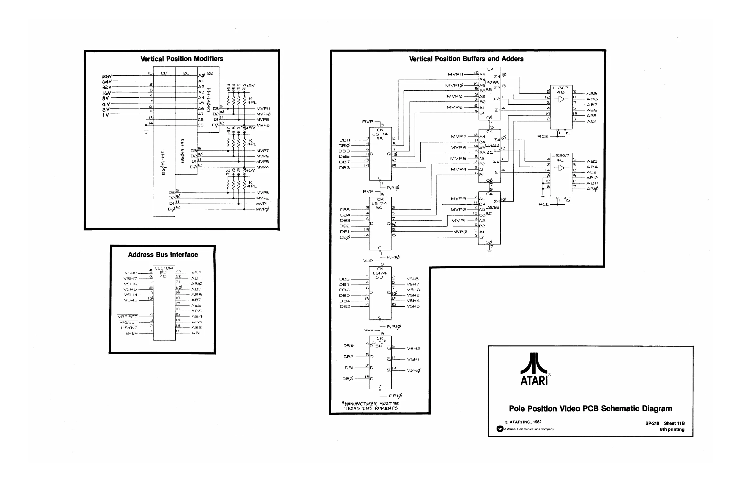
This page is a drawing, shown as the original scan.
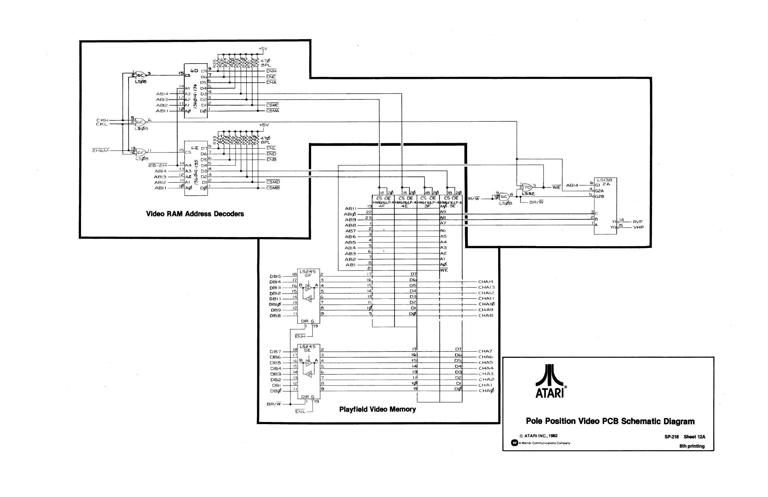
This page is a drawing, shown as the original scan.
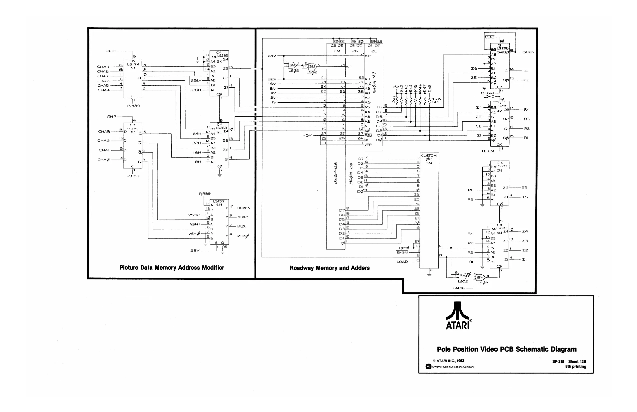
This page is a drawing, shown as the original scan.
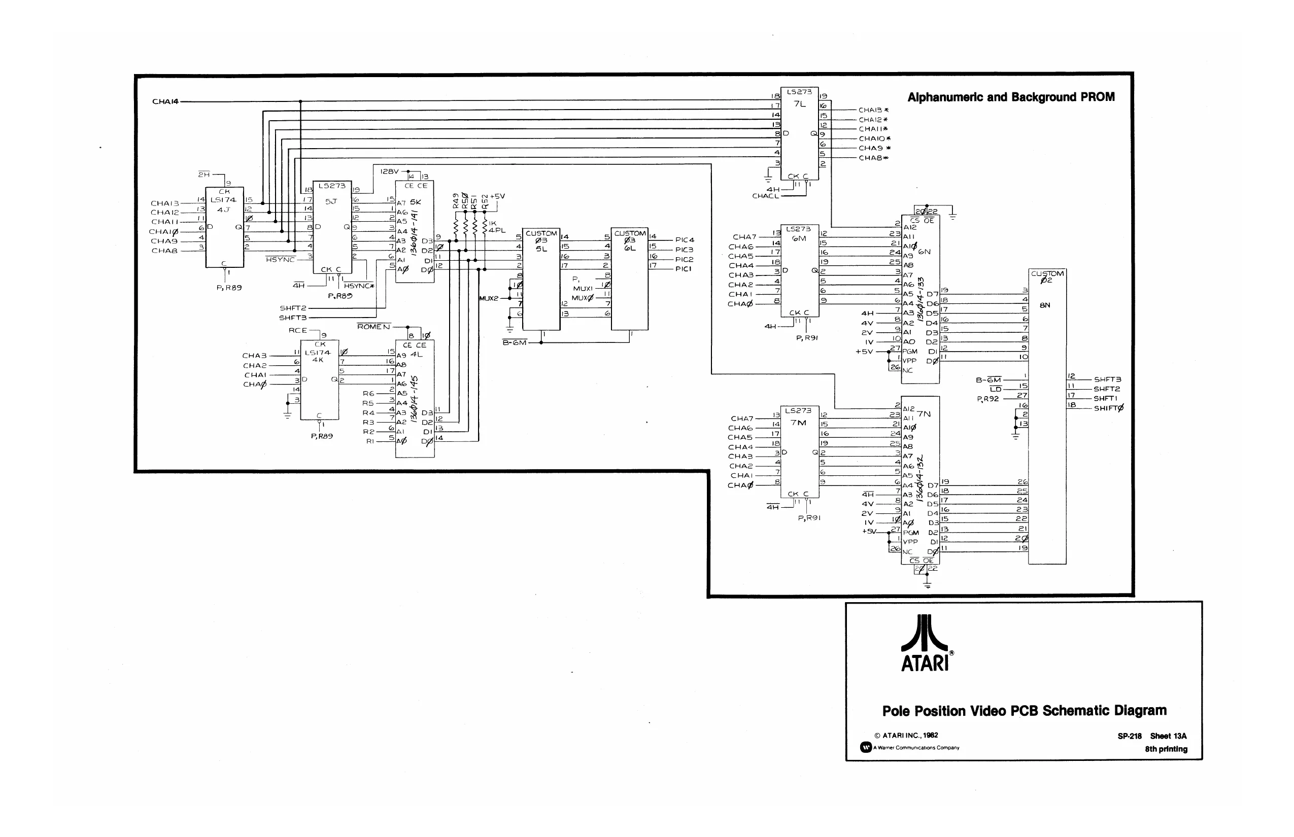
This page is a drawing, shown as the original scan.
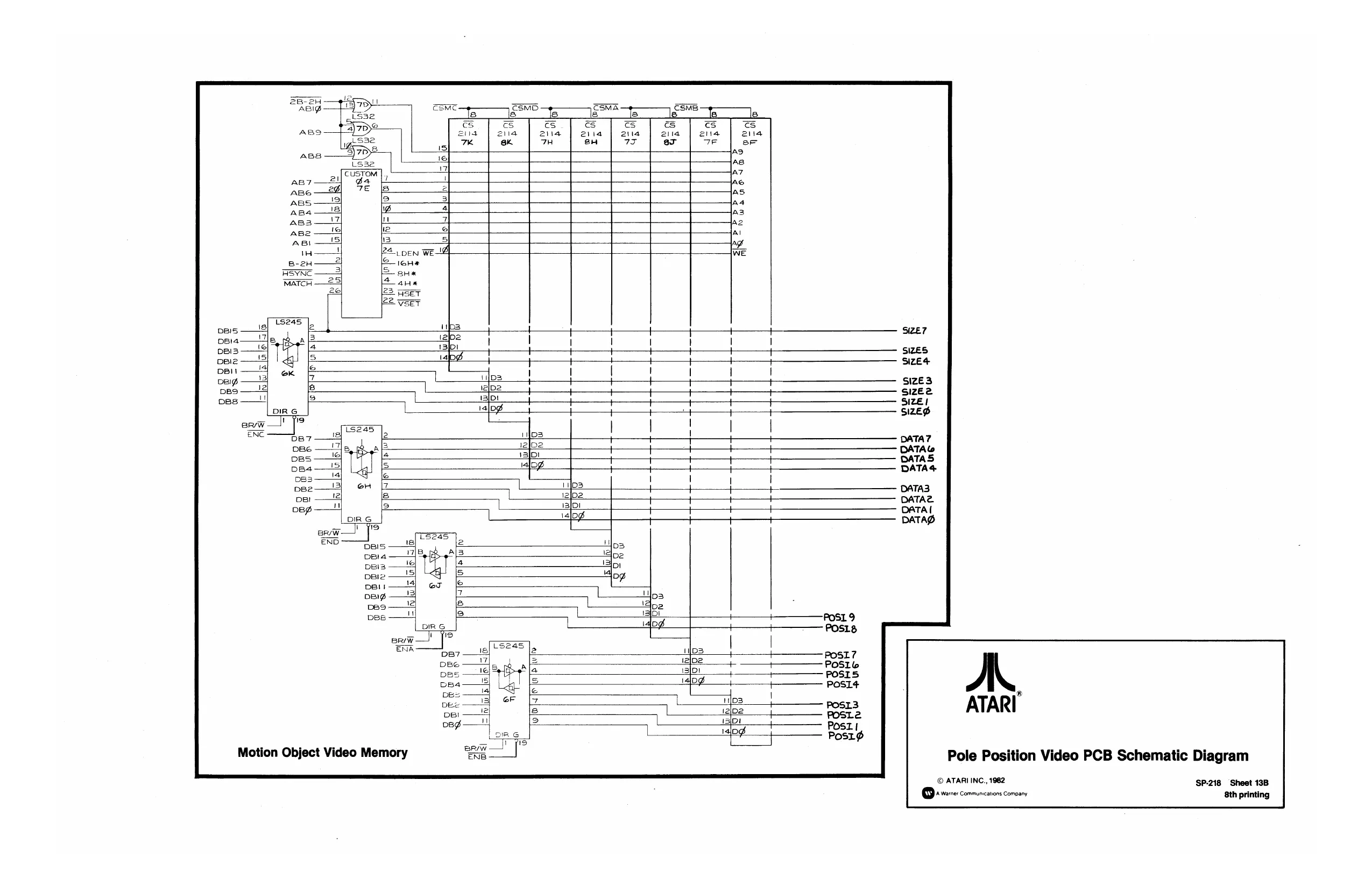
This page is a drawing, shown as the original scan.
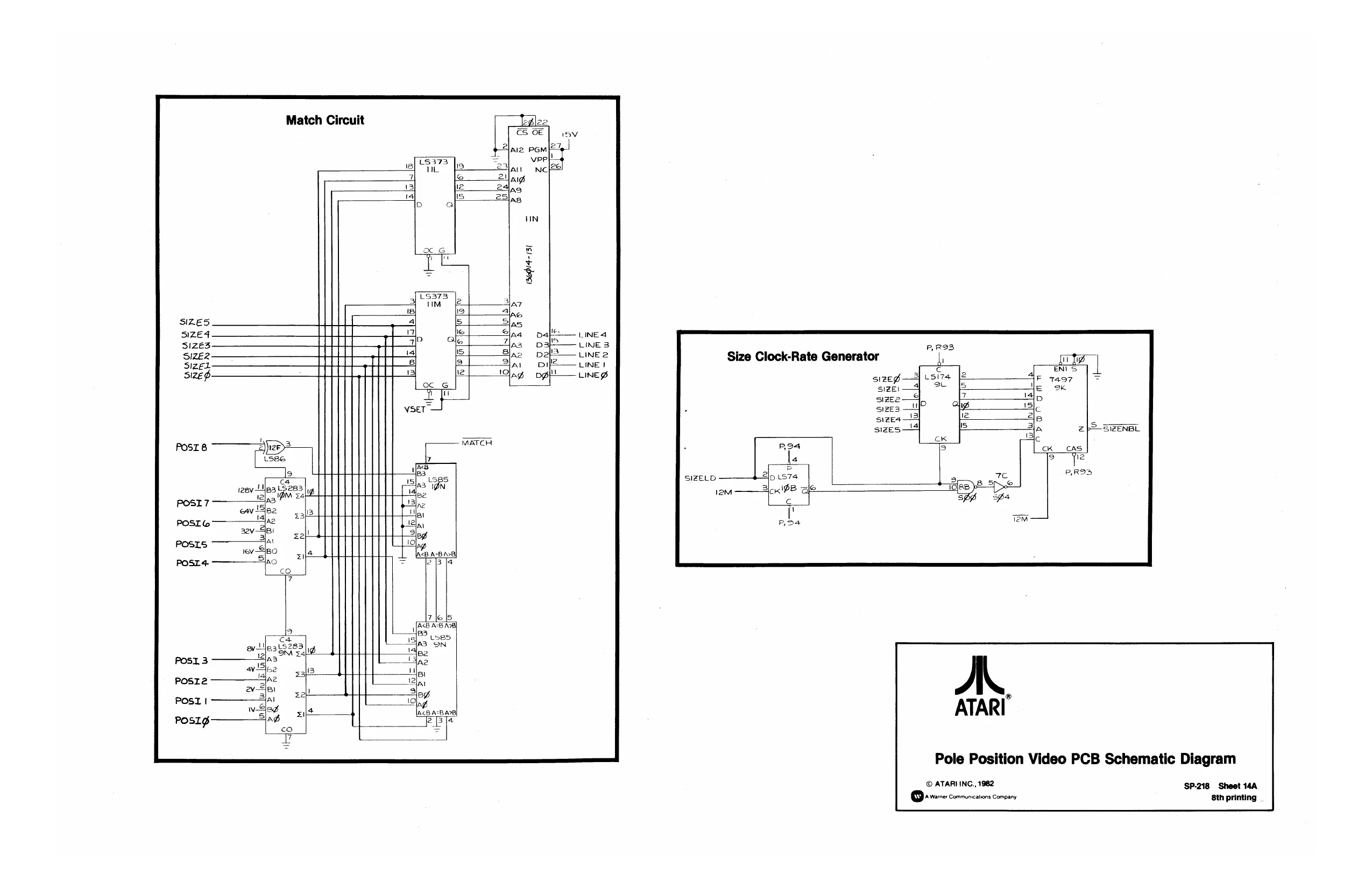
This page is a drawing, shown as the original scan.
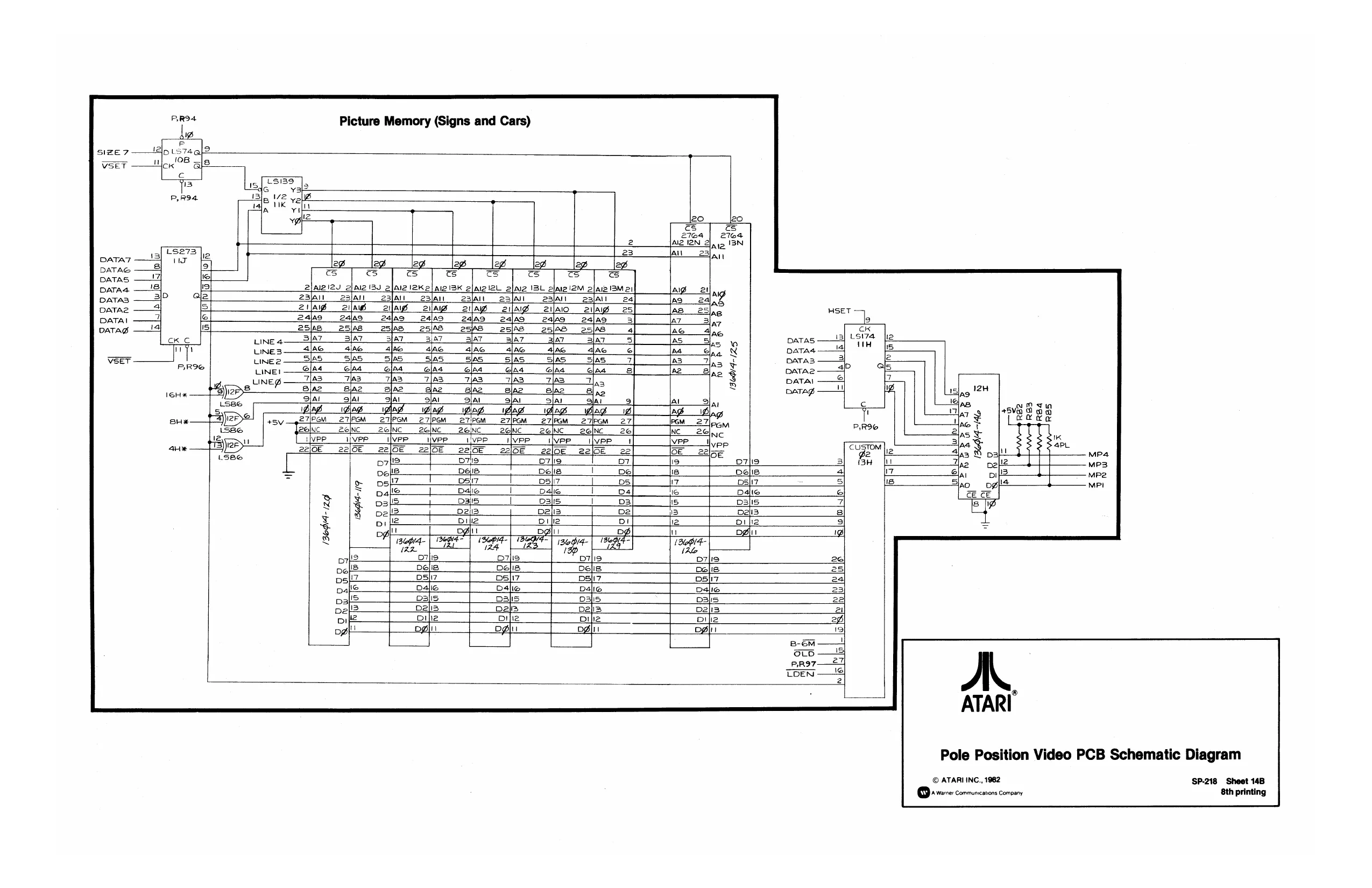
This page is a drawing, shown as the original scan.
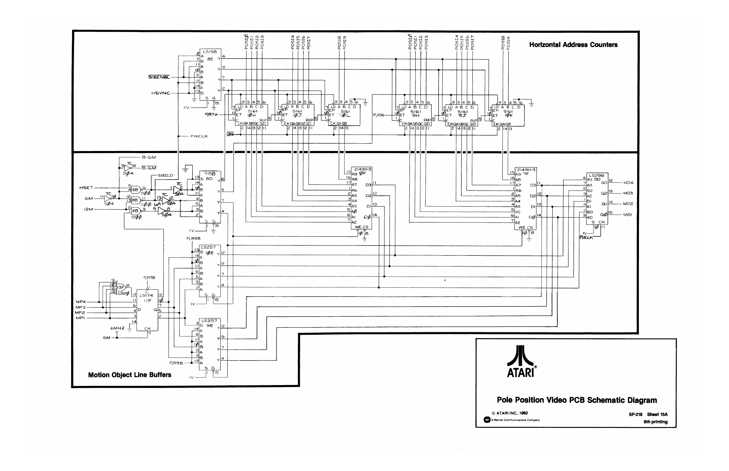
This page is a drawing, shown as the original scan.
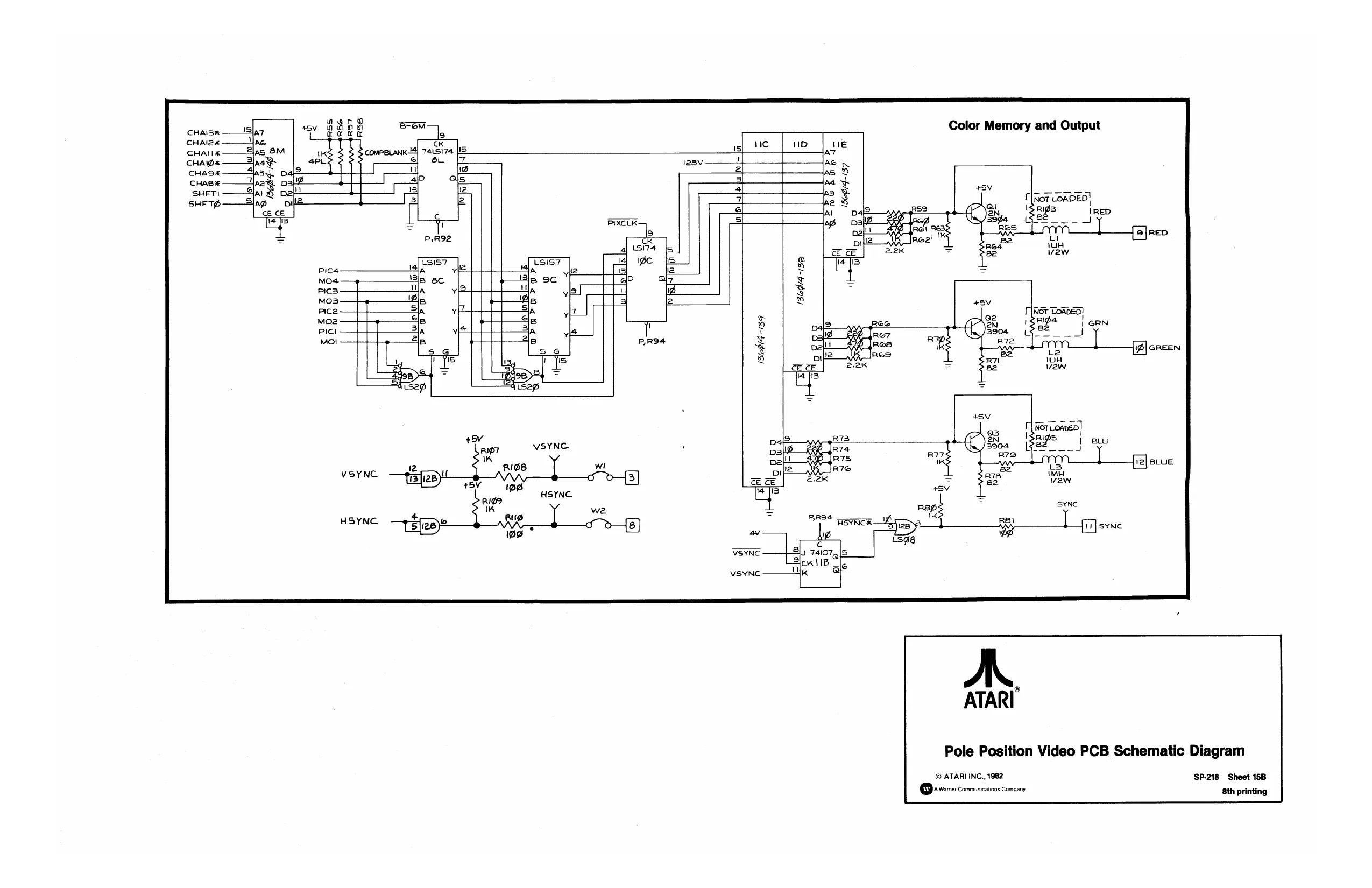
This page is a drawing, shown as the original scan.
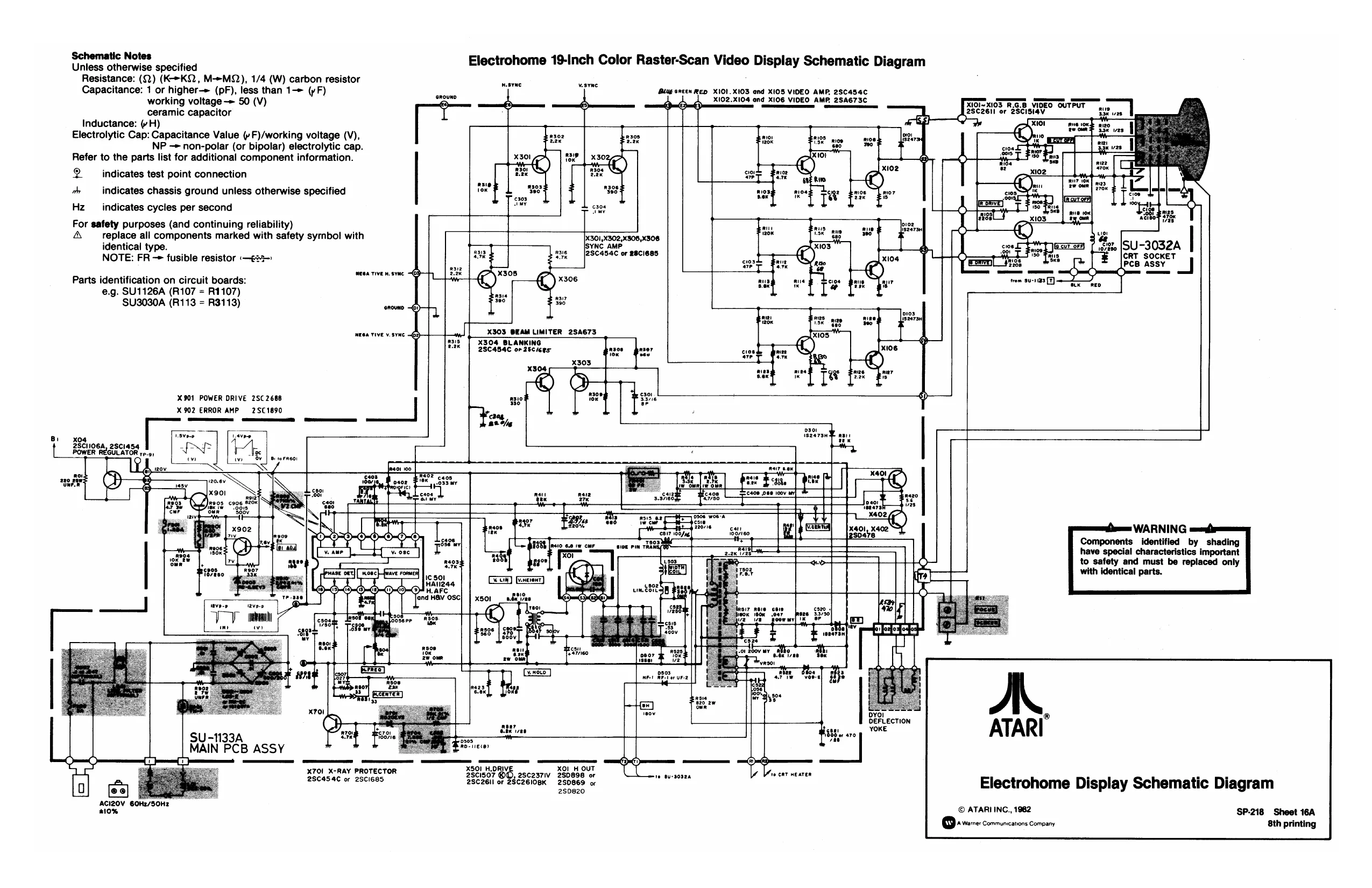
Schematic Notes Unless otherwise specified Resistance: (Q.) (K->KQ, MM), 1/4 (W) carbon resistor Capacitance: 1 or higher—> (pF), less than 1-> (yF) working voltage -> 50 (V) ceramic capacitor Inductance: ¢H) Electrolytic Cap: Capacitance Value (y F)/working voltage (V), NP — non-polar (or bipolar) electrolytic cap. Refer to the parts list for additional component information. 2 indicates test point connection oh indicates chassis ground unless otherwise specified Hz ___ indicates cycles per second For safety purposes (and continuing reliability) a replace all components marked with safety syrnbol with identical type.
maea vive v. seu 63
X901 POWER DRIVE 2SC 2688 % 902 ERROR AMP = 2SC 1890 Electrohome 19-Inch Color Raster-Scan Video Display Schematic Diagram
mesrne vsrne Blug oxen RED X101.X103 and XIOS VIDEO AMP, 2SC454C X102.X104 and XI06 VIDEO AMP. 2SA673C
ay ov RRR AP Seen ay aw 1. POWER REGULAT( a assorneo
; X303 GEAM LIMITER 2SA673 |X301,X302,x808,x308 ISYNC AMP 2SC454C or s8cie8s
X304 BLANKING 2SC4B4C or 25CKKes X10l~X103_R.G.8 VIDEO OUTPUT 28C2611 or 2SCISI4V
ISU-3032A | CRT SOCKET dpce assy trom 30-1123 [7] o-9 aK RED
X70I_ X-RAY PROTECTOR 2SC454C or 2SCI685
ACIZ0V 6OH/S0Hz 210% Ca) ace] xSO1 wire
byor DEFLECTION YOKE
3508 RD 11e(0) Se X50! H.ORIVI XO1_H OUT 251507 WO, 2sc2371v 280898 or 2SC2EIl or ZSC2EIOBK 250869 or 280820 more fo CRT HEATER
© ATARI INC., 1982 vere commons Cnosny ‘WARNING Components identified by shading have special characteristics important to safety and must be replaced only with identical parts.
ATARI
Electrohome Display Schematic Diagram
SP-218 Sheet 16A 8th printing
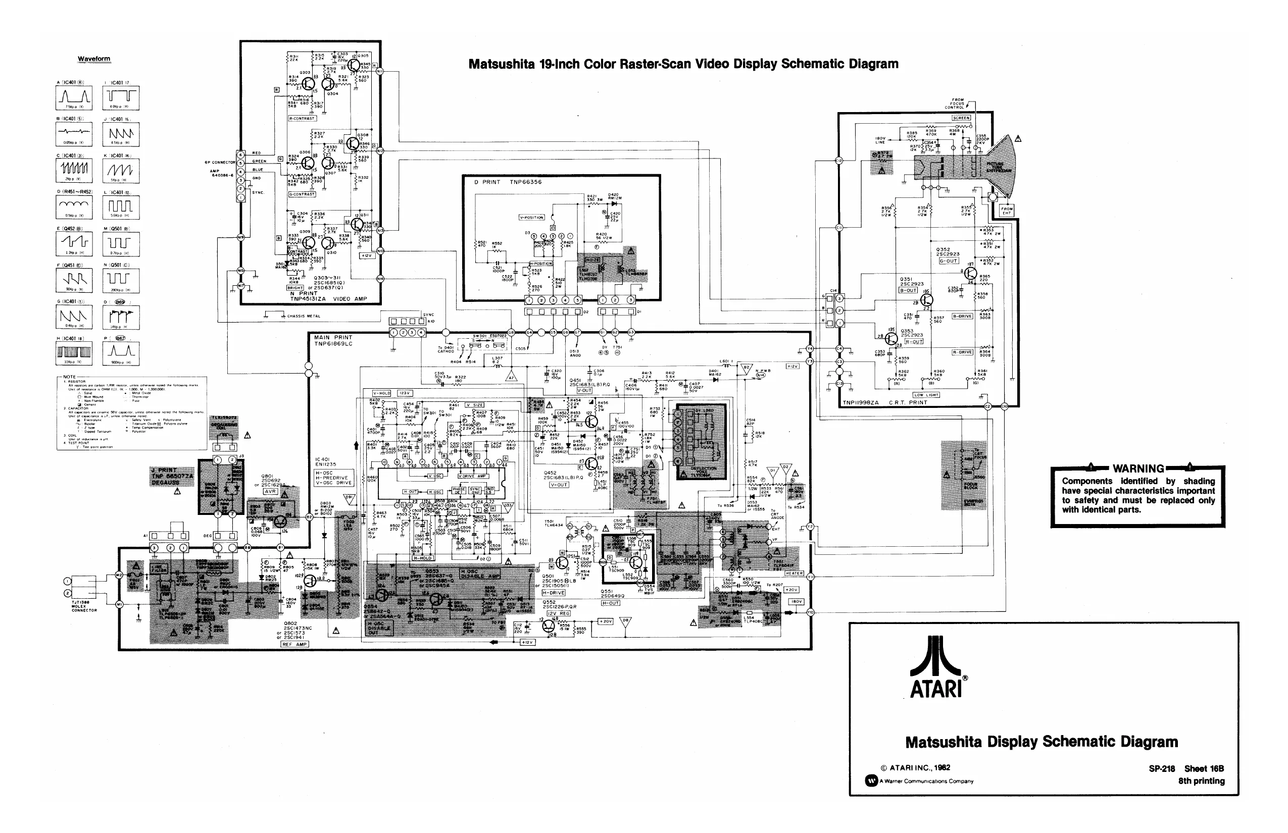
This page is a drawing, shown as the original scan.