Millipede SP-217 2nd Printing
Millipede (Atari, 1982) · Schematic Package · 21 pages · 54 sections · original scan
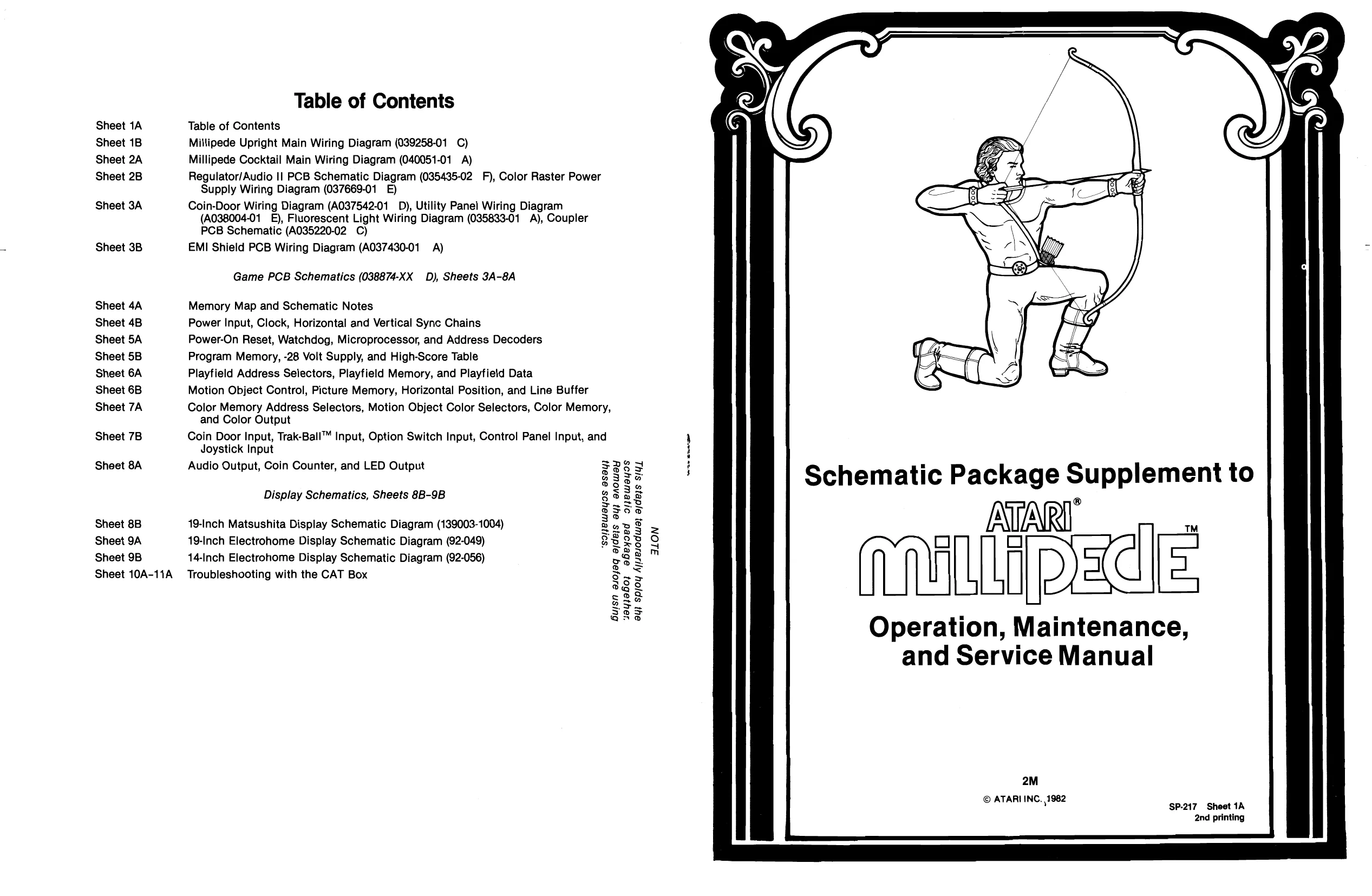
Table of Contents
Sheet 1A Table of Contents Sheet 1B Millipede Upright Main Wiring Diagram (039258-01 C) Sheet 2A Millipede Cocktail Main Wiring Diagram (040051-01 A) Sheet 2B Regulator/Audio Il PCB Schematic Diagram (035435-02 F), Color Raster Power Supply Wiring Diagram (037669-01 &) Sheet 3A Coin-Door Wiring Diagram (A037542-01 D), Utility Panel Wiring Diagram (A038004-01 £), Fluorescent Light Wiring Diagram (035833-01 A), Coupler PCB Schematic (A035220-02 C) Sheet 3B EMI Shield PCB Wiring Diagram (A037430-01 A)
Game PCB Schematics (038874-XX D), Sheets 3A-8A
Sheet 4A Memory Map and Schematic Notes Sheet 4B Power Input, Clock, Horizontal and Vertical Sync Chains Sheet 5A Power-On Reset, Watchdog, Microprocessor, and Address Decoders Sheet 5B Program Memory, -28 Volt Supply, and High-Score Table Sheet 6A Playfield Address Selectors, Playfield Memory, and Playfield Data Sheet 6B Motion Object Control, Picture Memory, Horizontal Position, and Line Buffer Sheet 7A Color Memory Address Selectors, Motion Object Color Selectors, Color Memory, and Color Output Sheet 7B Coin Door Input, Trak-Ball™ Input, Option Switch Input, Control Panel Input, and Joystick Input Sheet 8A Audio Output, Coin Counter, and LED Output = g oD Display Schematics, Sheets 8B-9B 8 o Sheet 8B 19-Inch Matsushita Display Schematic Diagram (139003-1004) a Sheet 9A 19-Inch Electrohome Display Schematic Diagram (92-049) 3 Sheet 9B 14-Inch Electrohome Display Schematic Diagram (92-056) Sheet 10A-11A Troubleshooting with the CAT Box Bujsn asojaq ajders ayy erowey yeyjabo} abeyoed ojjewayos ay} spjoy Ajsesodwia} ajde}s siyL
ALON Schematic Package Supplement to ATARI MOLY
Operation, Maintenance, and Service Manual
2M ATARI INC. 1982 . ’ SP-217 Sheet 1A
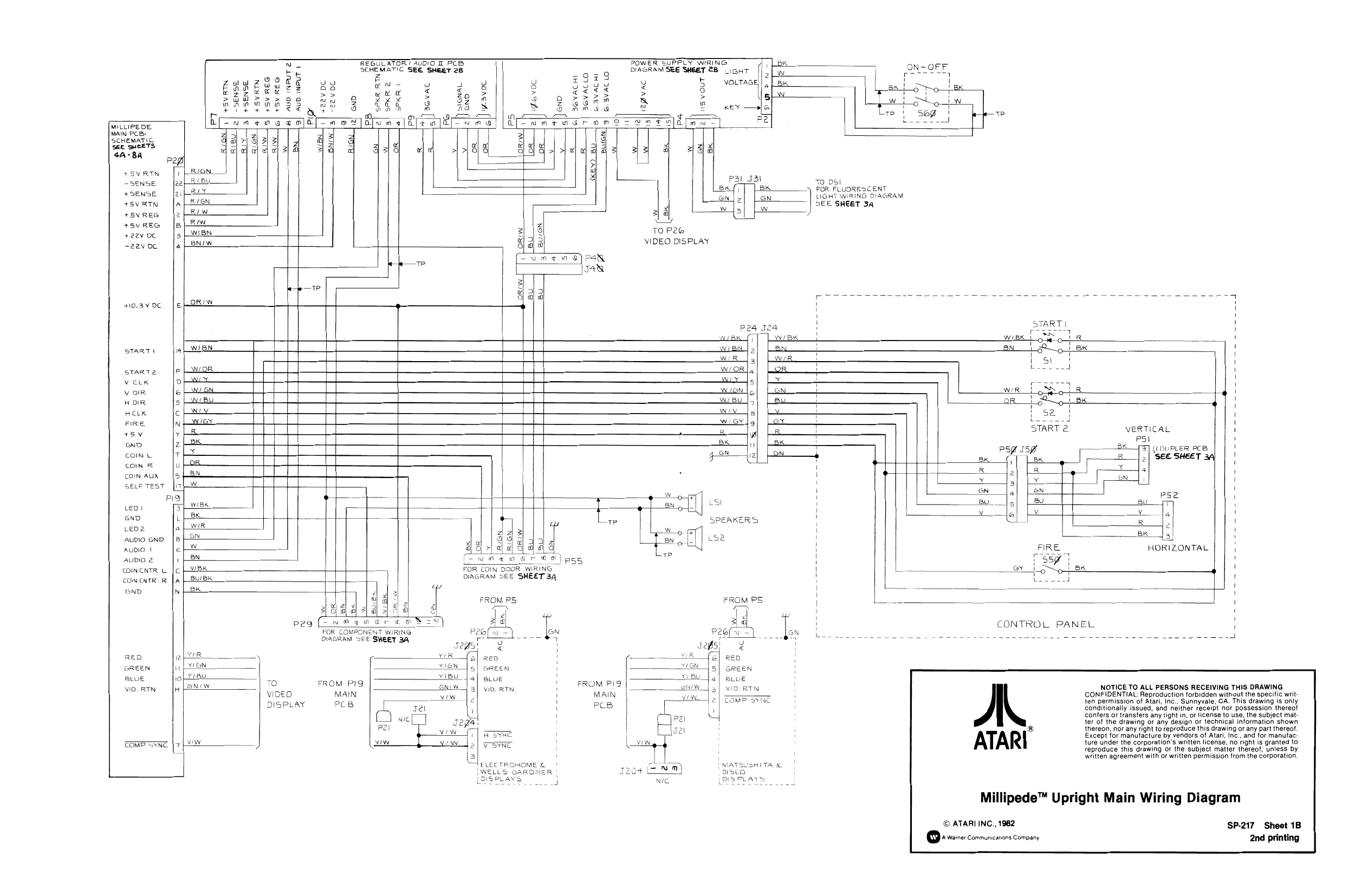
This page is a drawing, shown as the original scan.
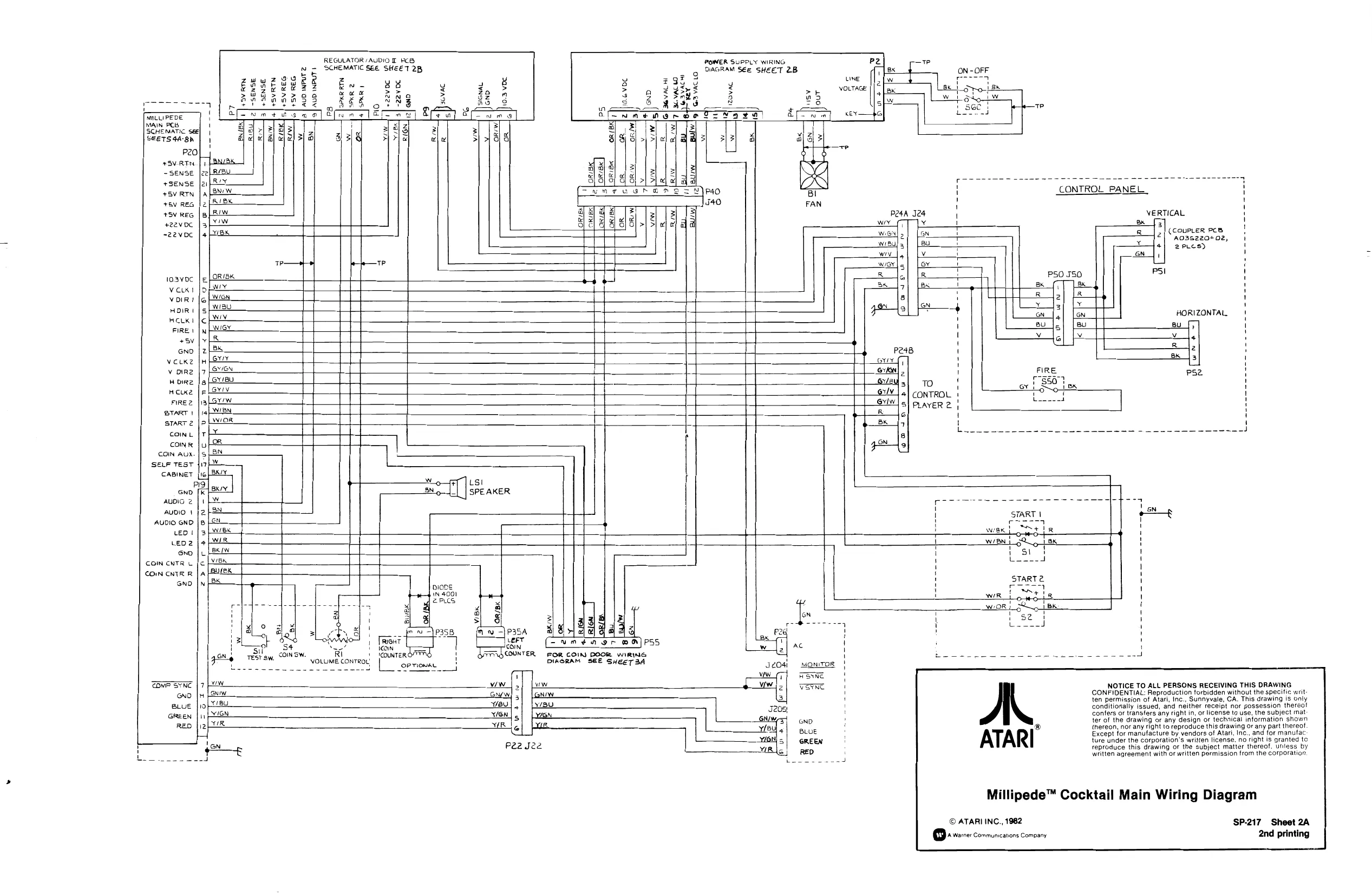
This page is a drawing, shown as the original scan.
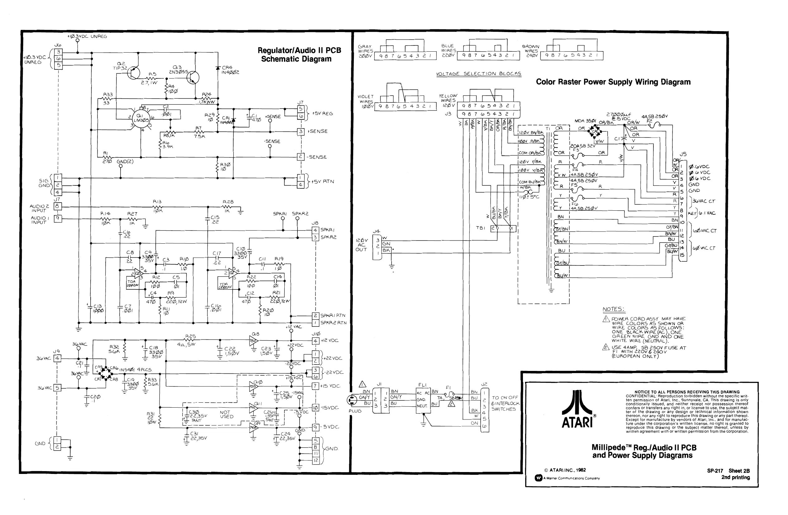
This page is a drawing, shown as the original scan.
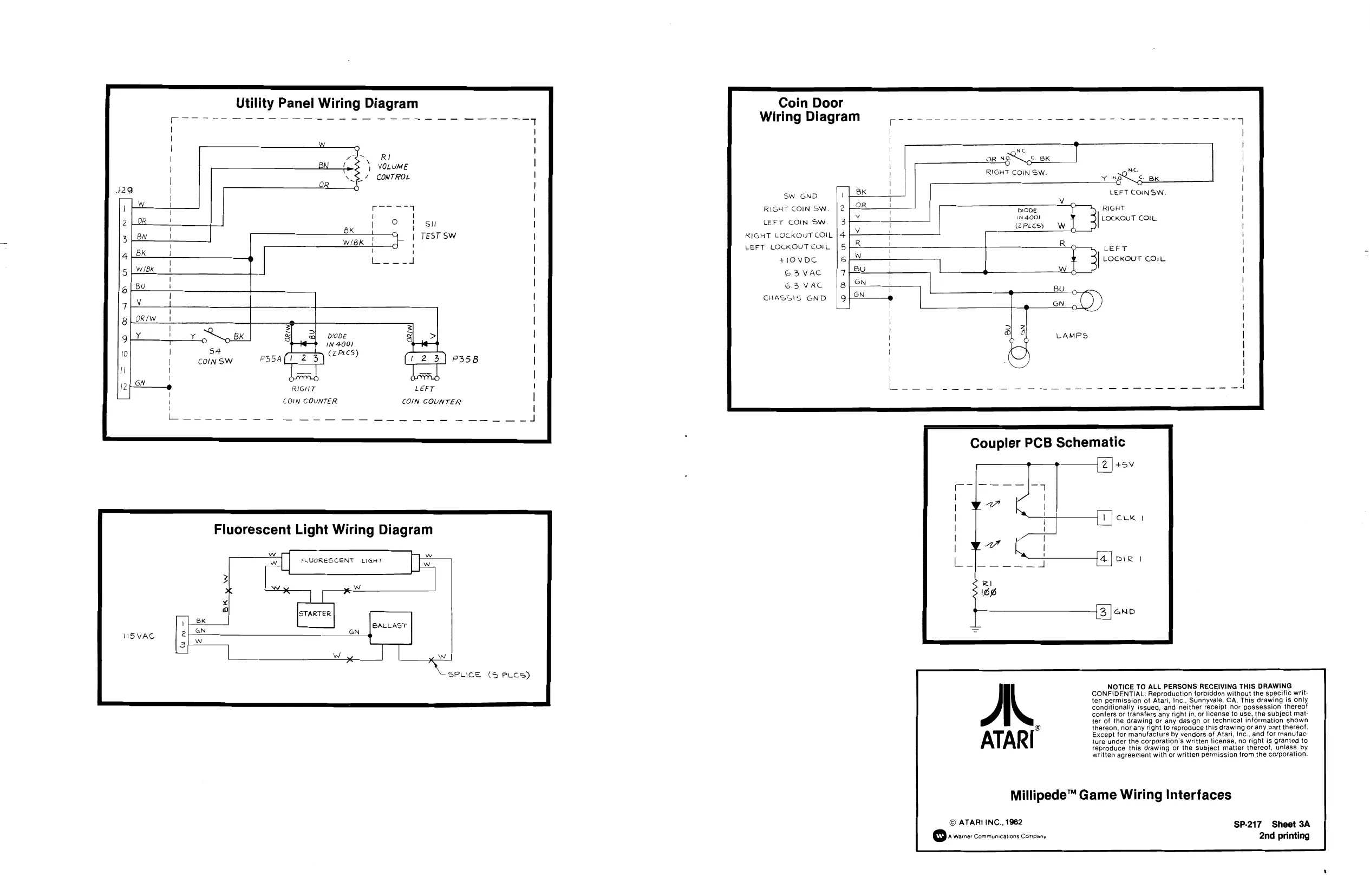
Utility Panel Wiring Diagram Coin Door
Wiring Diagram
Ne nS cs yOLUME on NS 8K ne RIGHT COIN SW. x naQ ox SW GND LEFT COINSW,
RIGHT COIN SW DIODE RIGHT sil LEFT COIN SW 400! | Locxour com, . j (rics) _W TEST SW RIGHT LOCKOUT COIL LEFT LOCKOUT COIL LEFT +10VDC | tockour core 6.3 VAC 6.3 VAC
CHASSIS GND
y ww Bk DIODE S4 in 3001 COIN SW atl
RIGHT LEFT
COIN COUNTER COIN COUNTER
Fluorescent Light Wiring Diagram
loraerer
@ALLAST MSVAC on
Wg a SPLICE (5 PLCS)
confers or transfers any right in, or license to use, the subject mat ter of the drawing or any design or technical information shown ® thereon, nor any right to reproduce this drawing or any part thereof. Except for manufacture by vendors of Atari, Inc., and for manufac: ture under the corporation's written license, no right is granted to reproduce this drawing or the subject matter thereof, unless by written agreement with or written permission from the corporation. NOTICE TO ALL PERSONS RECEIVING THIS DRAWING CONFIDENTIAL: Reproduction forbidden without the specific writ ten permission of Atari, Inc., Sunnyvale, CA, This drawing is only conditionally issued, and neither receipt nor possession thereot
Millipede™ Game Wiring Interfaces
© ATARI INC., 1982 SP-217 Sheet 3A
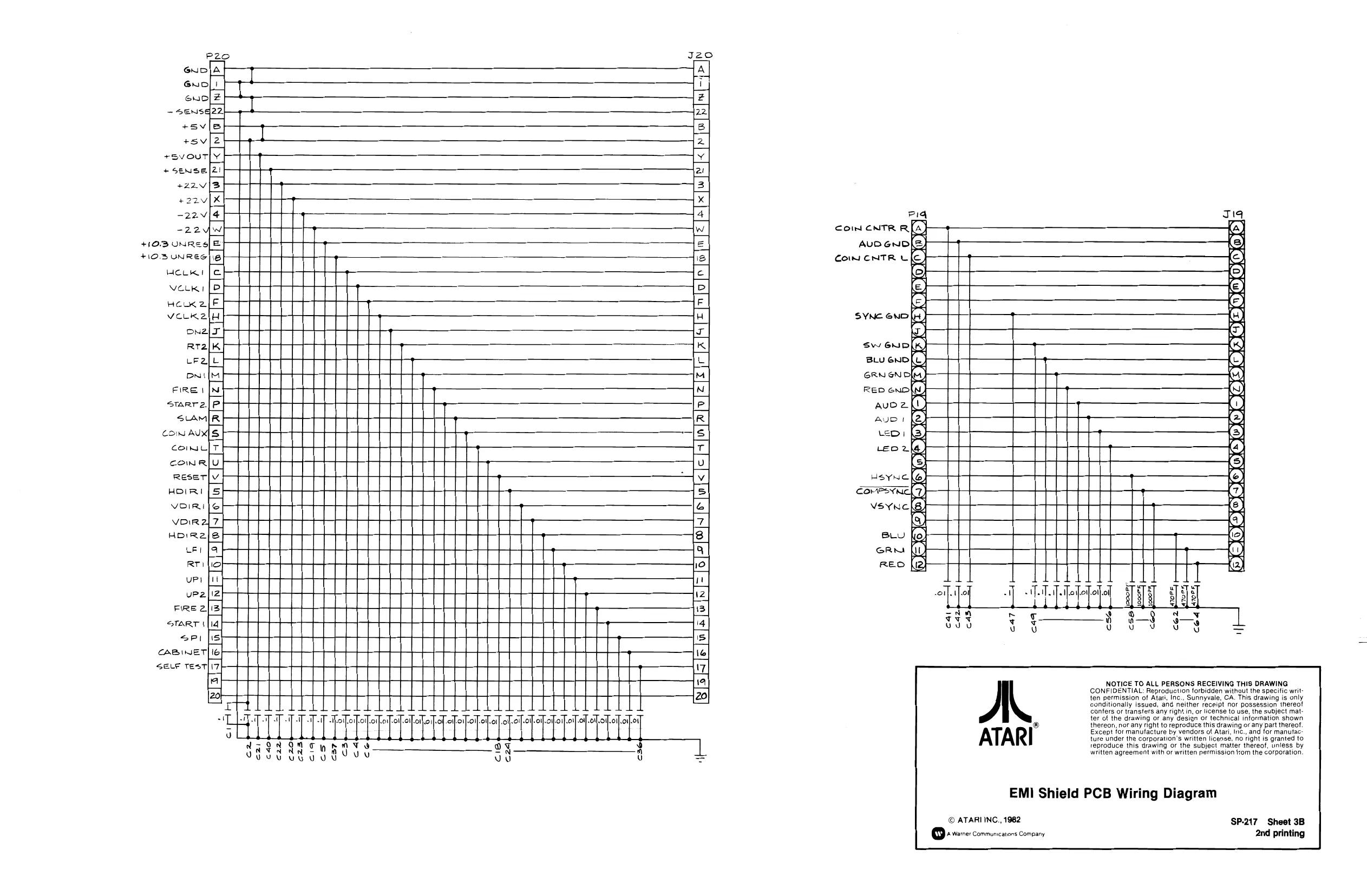
This page is a drawing, shown as the original scan.
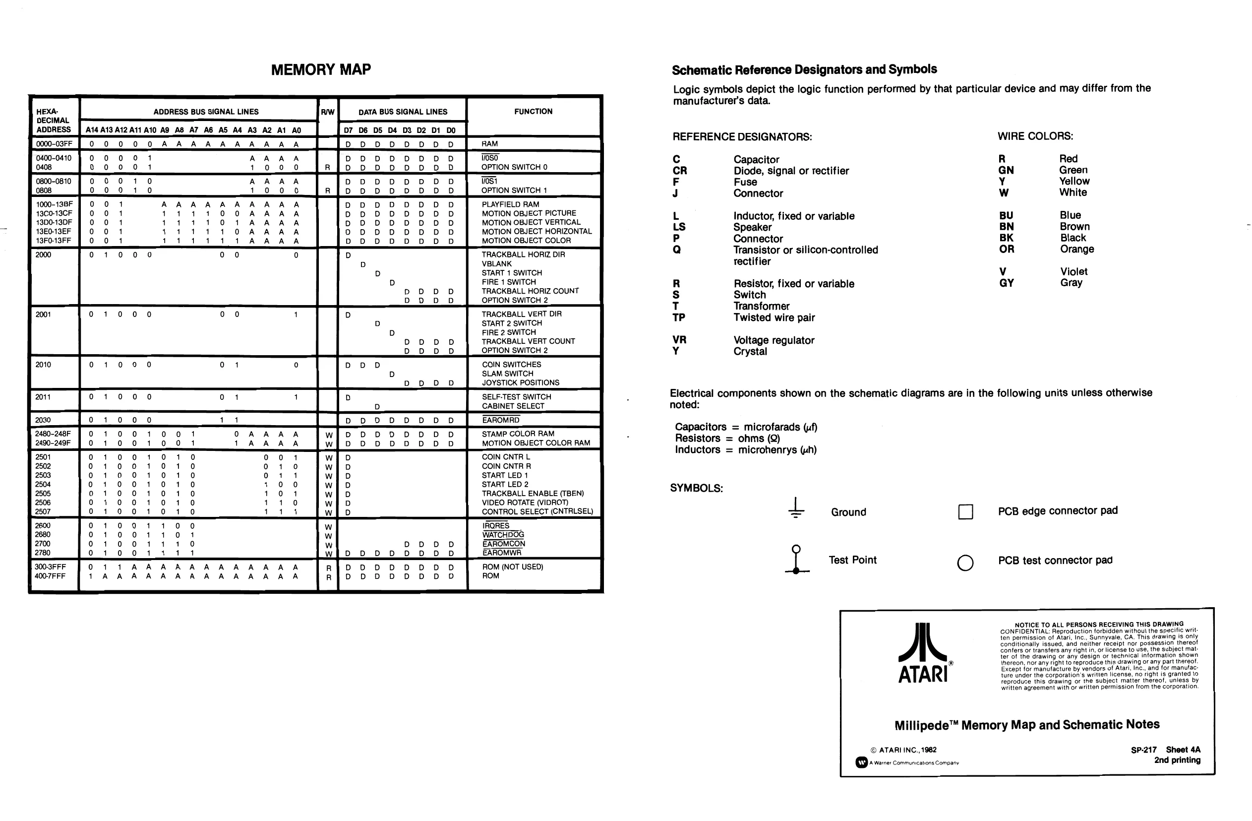
MEMORY MAP
DATA BUS SIGNAL LINES FUNCTION
ae ADDRESS BUS SIGNAL LINES
A14 A13 A12 A11 A10 AQ AS A7 AG AS A4 A3 A2 Al AD
1000-13BF 13C0-13CF 13D0-13DF 13E0-13EF 13F0-13FF lo loo fo loofoo D DD
D DD D DUD
D DoD D DO
D DoD D DD D DoD D DoD D DoD oo000foo0 V0S0 OPTION SWITCH 0
WOS1 OPTION SWITCH 1
PLAYFIELD RAM MOTION OBJECT PICTURE MOTION OBJECT VERTICAL MOTION OBJECT HORIZONTAL MOTION OBJECT COLOR so000foo0foo]o go000fon0foolo
Schematic Reference Designators and Symbols
Logic symbols depict the logic function performed by that particular device and may differ from the manufacturer's data.
TRACKBALL HORIZ DIR VBLANK START 1 SWITCH FIRE 1 SWITCH TRACKBALL HORIZ COUNT OPTION SWITCH 2
TRACKBALL VERT DIR START 2 SWITCH FIRE 2 SWITCH TRACKBALL VERT COUNT OPTION SWITCH 2
DoD COIN SWITCHES D SLAM SWITCH DDO D JOYSTICK POSITIONS
SELF-TEST SWITCH CABINET SELECT
EAROMRD
STAMP COLOR RAM MOTION OBJECT COLOR RAM
COIN CNTR L COIN CNTR R START LED 1 START LED 2 TRACKBALL ENABLE (TBEN) VIDEO ROTATE (VIDROT) CONTROL SELECT (CNTRLSEL) IRQRES WATCHDOG EAROMCON EAROMWA
ROM (NOT USED) ROM °
i oo}o volo volo solo volo volo oofo joc0000D}oN
loo oofo oofo volo oofo oo vofoo vofoo cofoo po=fezzefezzzzzzfe<{ {| | | | | Pt 2] o ; o joo i i= REFERENCE DESIGNATORS: WIRE COLORS:
| c | Capacitor | R | Red |
| CR | Diode, signal or rectifier | GN | Green |
F Fuse Y Yellow
J Connector w White
| L | Inductor, fixed or variable | BU | Blue |
| Ls | Speaker | BN | Brown |
P Connector BK Black
| Q | Transistor or silicon-controlled | OR | Orange |
rectifier
Vv Violet
| R | Resistor, fixed or variable | GY | Gray |
Ss Switch T Transformer TP Twisted wire pair
VR Voltage regulator Y Crystal
Electrical components shown on the schematic diagrams are in the following units unless otherwise noted:
Capacitors = microfarads (uf) Resistors = ohms (Q) Inductors = microhenrys (uh)
SYMBOLS:
Ground
1 Test Point oo
AL ATARI PCB edge connector pad
PCB test connector pad
NOTICE TO ALL PERSONS RECEIVING THIS DRAWING CONFIDENTIAL: Reproduction forbidden withou\ the specific writ. ten permission of Atari, Inc., Sunnyvale, CA. This drawing is only conditionally issued, and neither receipt nor possession thereof Confers or transfers any right in, or license to use, the subject mat ter of the drawing or any design or technical information shown thereon, nor any right to reproduce this drawing or any part thereof, Except for manufacture by vendors of Atari, Inc., and for manufac: ture under the corporation's written license, no right is granted 10 reproduce this drawing or the subject matter thereof, unless by written agreement with or written permission from the corporation.
Millipede™ Memory Map and Schematic Notes
© ATARI INC.,1982 SP-217 Sheet 4A
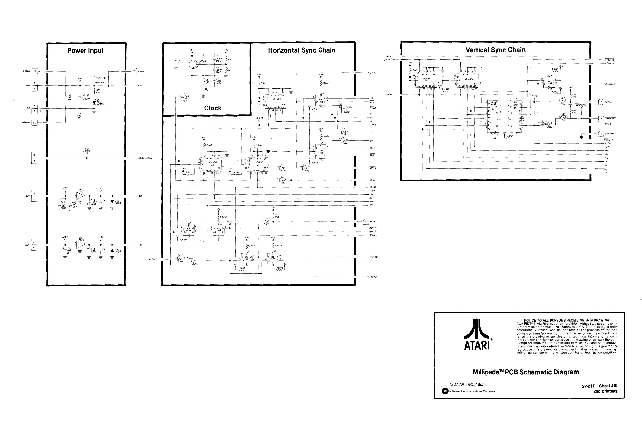
This page is a drawing, shown as the original scan.
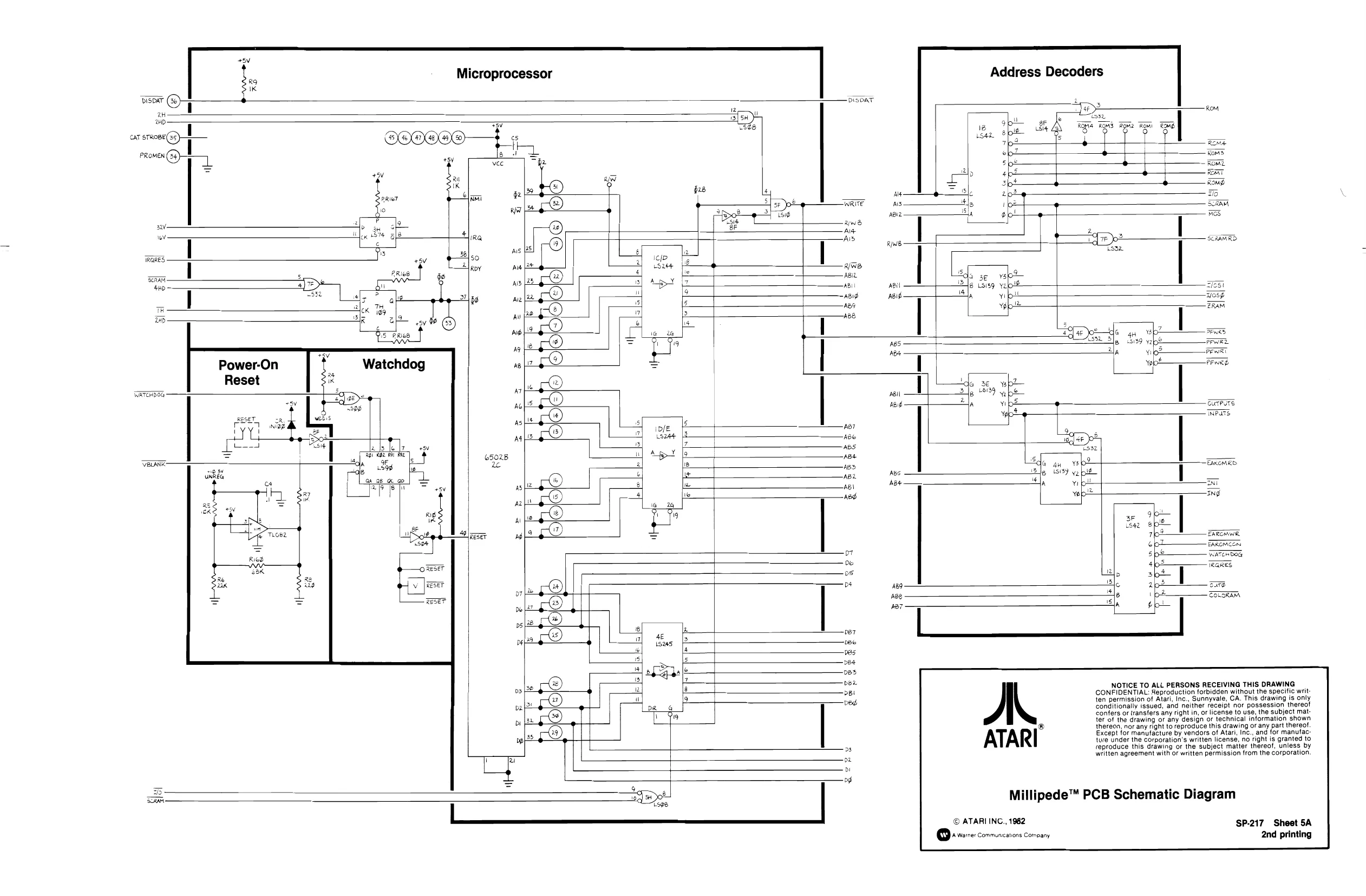
This page is a drawing, shown as the original scan.
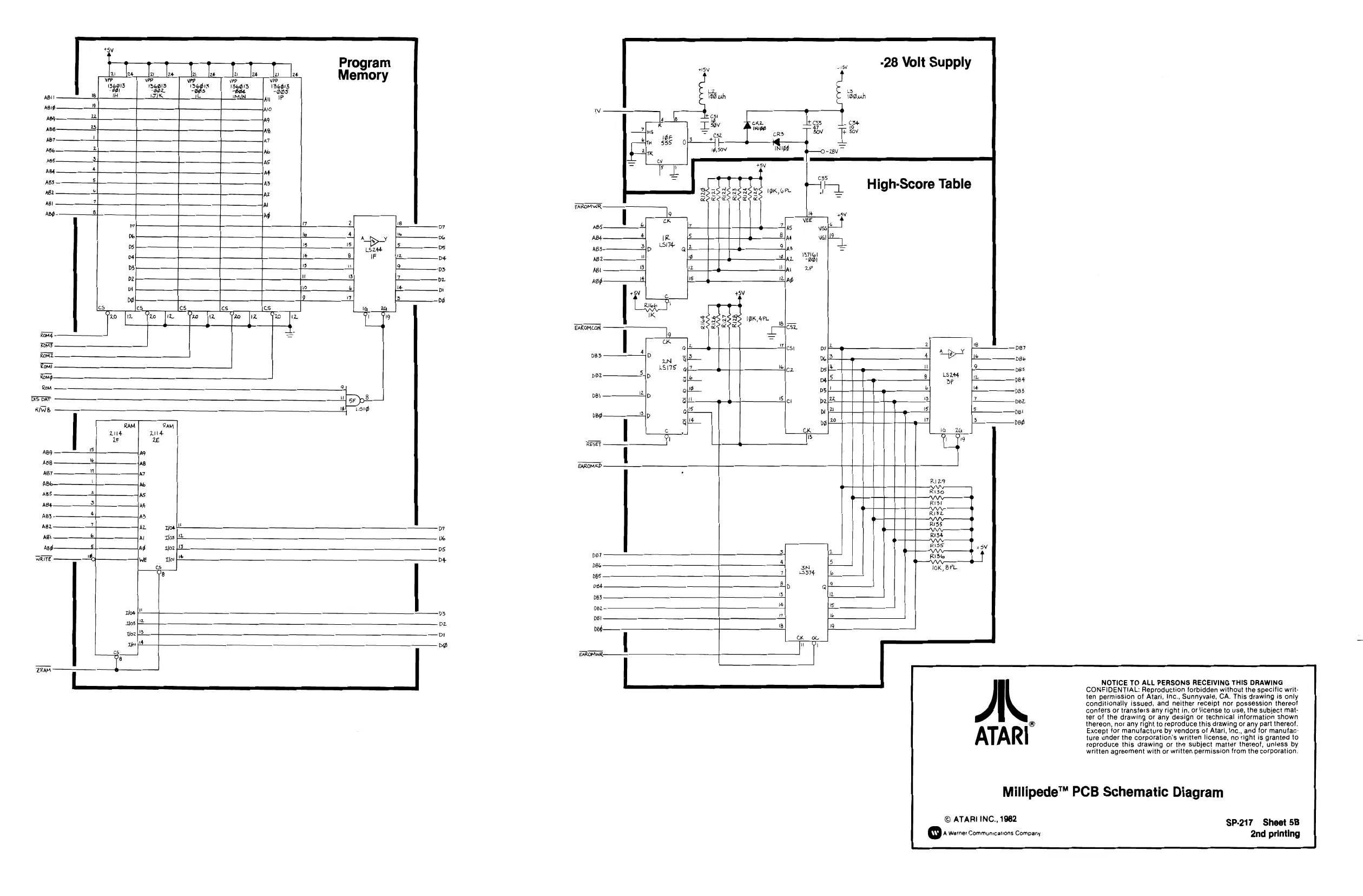
This page is a drawing, shown as the original scan.
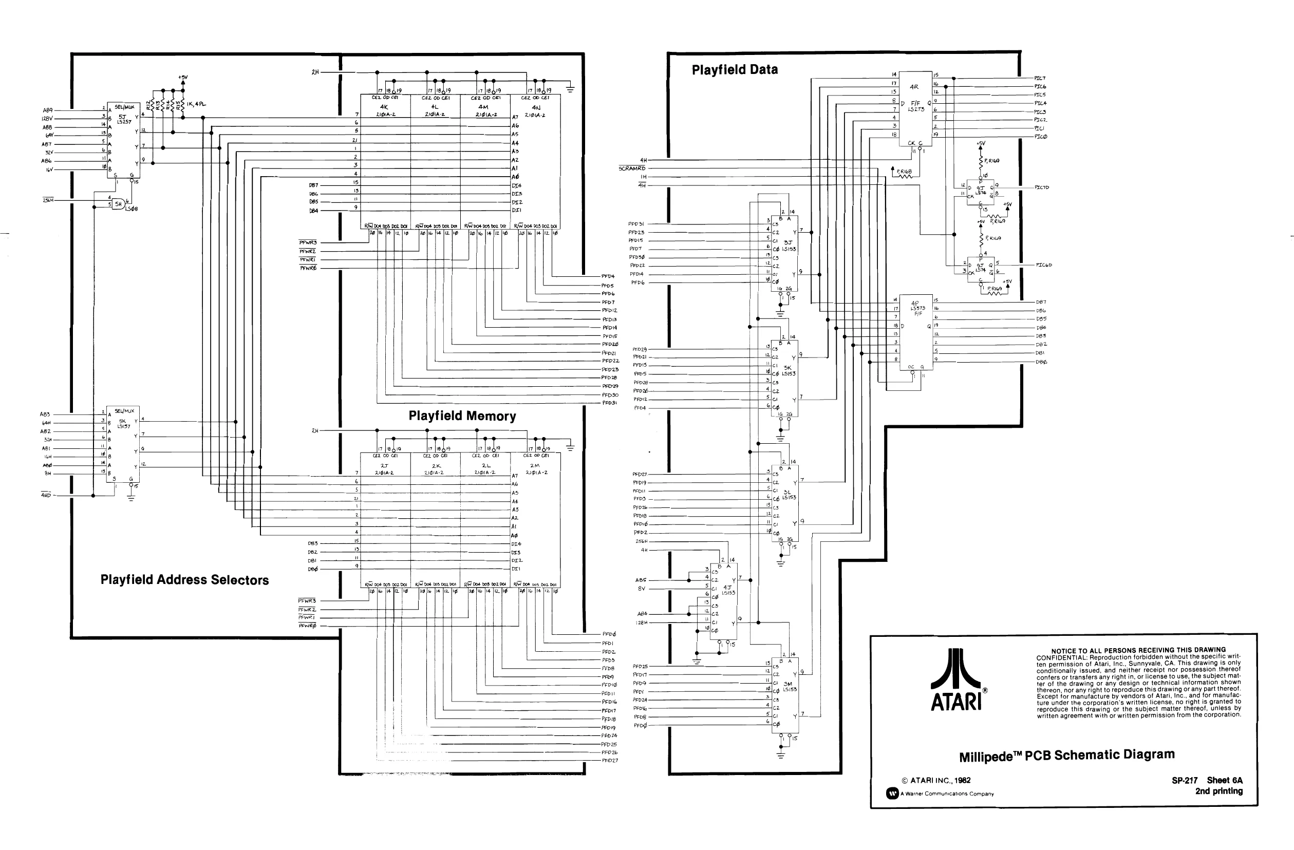
This page is a drawing, shown as the original scan.
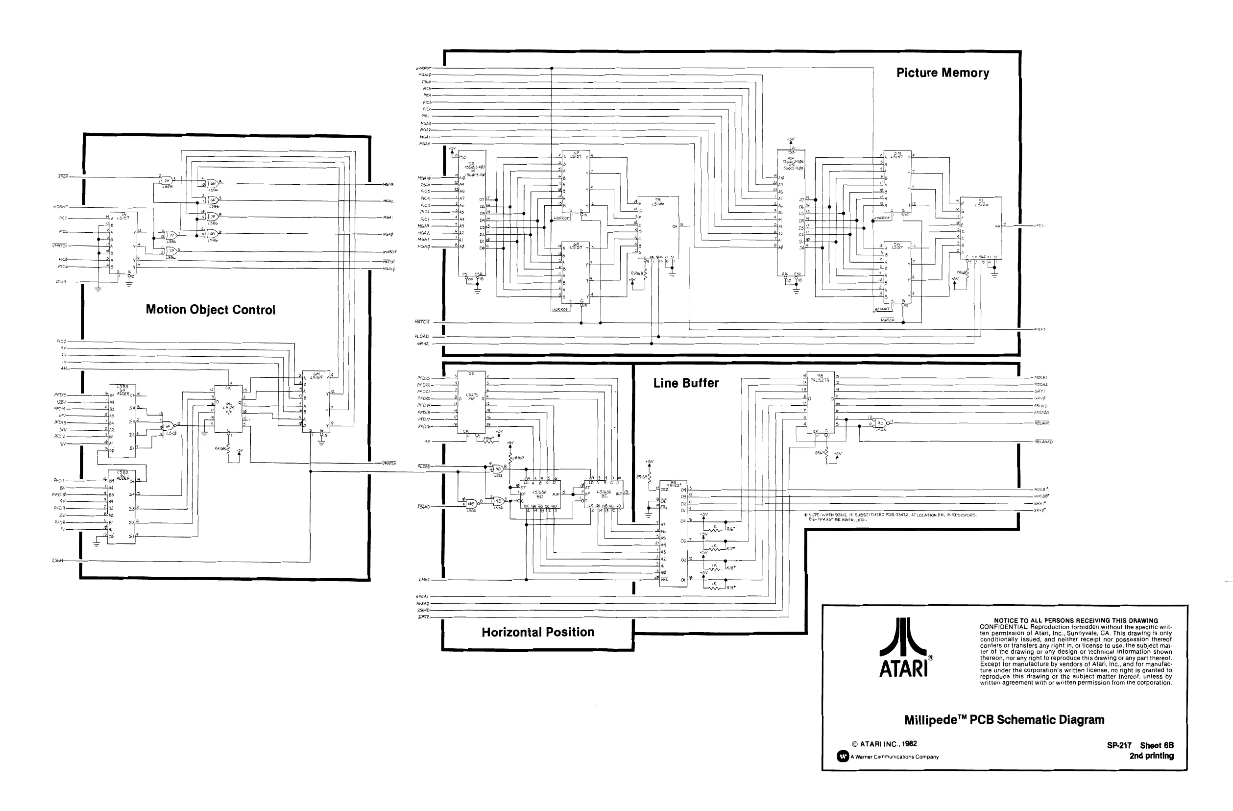
This page is a drawing, shown as the original scan.
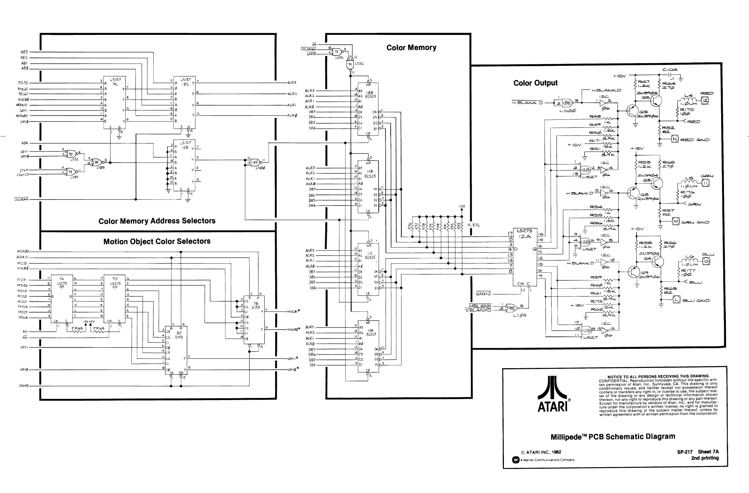
This page is a drawing, shown as the original scan.
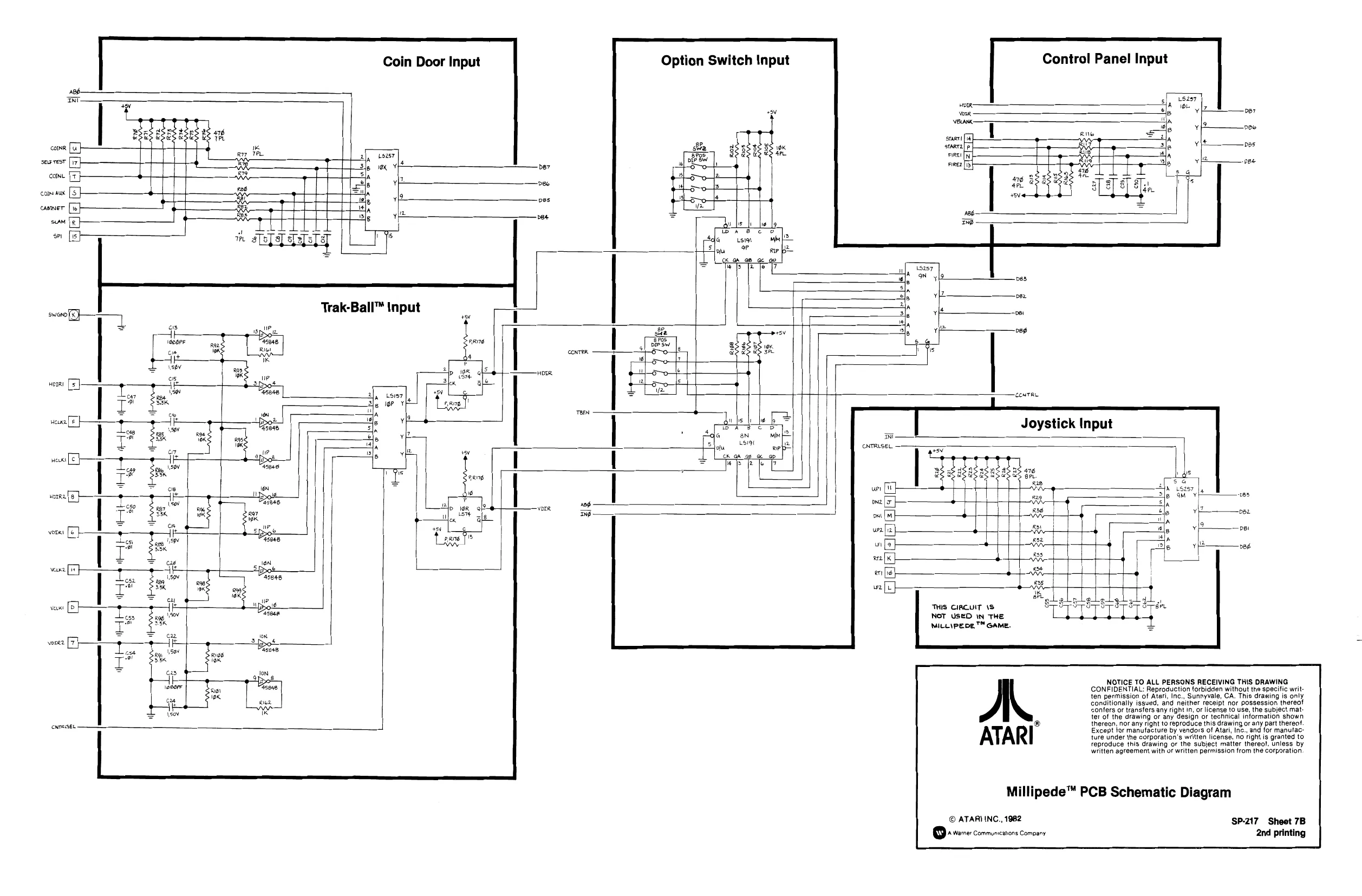
Control Panel Input
Coin Door Input
Option Switch Input
coin
sexrest bs? cae
com Auk
casmer eum TS] vet
oi
h le
£15
ewe 3 fe | “le ie ov oy oes Ae 85 $8.38 10
rahe
wore s | is
een
Joystick Input
int
DIR. aad ang
veux
eat ‘THs CIRCUIT 1S NOT USED IN THE MILLIPEDE ™ GAME.
NOTICE TO ALL PERSONS RECEIVING THIS DRAWING CONFIDENTIAL: Reproduction forbidden without the specific written permission of Atari, Inc., Sunnyvale, CA. This drawing is only Conditionally isgued, and neither receipt nor possession thereot Confers or transfers any right n, or licence o use, the subject matter of the drawing or acy design of technical iniormation shown cnet. thereon nor any "ght to reproduce this drawing or ary part there! ® Except far manufacture by vendors of Atari, Inc., and for manutacture under the corporation's written license, no right is granted to reproduce this drawing or the subject matter thereo}, unless by written agreement with of written permission from the corporation
Millipede™ PCB Schematic Diagram
ATARI INC., 1982 SP-217 Sheet 7B fw") JA Warner Communications Company 2nd printing
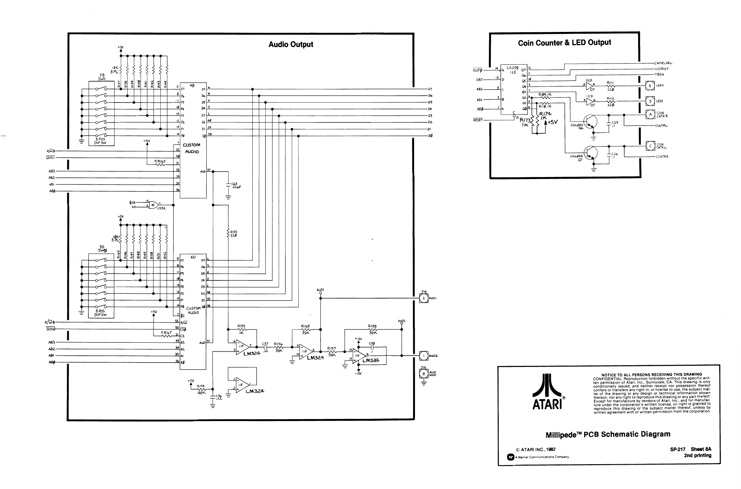
Audio Output Coin Counter & LED Output
ATRLSEL arp —4YJa $297 a7} vioRoT is af BEN ar: Sm 15
| fed | 2 | 4 | Lee | |
| PL | Abt. | 07 | 226 | Mt |
| DS | abr | LeDI |
Dt Bp 05 com Ys ERTRR
| Da | RESET. | Rr |
I CONTR
op
| als. | 2 | con |
AUDIO CNTR ost 36 I BRIT | a conreR
| 85 | 2) | nw |
- 4 31 x
- x Det us isst +5v
iss Tho
4D o7/e % os|4 o os 2 ane 79 DI { 2 urs ul on HP csr = | viesw rR alg. AUD ale ag ype Tess soley Las nies PRCT me l kes HK ABS- ‘AB2sa! JAuoz nop
- uJ NOTICE TO ALL PERSONS RECEIVING THIS DRAWING wy CONFIDENTIAL: Reproduction forbidden without the specific writ-
ast uF en permission of Atari, Inc. Sunnyvale, CA. This drawing is only
e324 conditionally issued, and neither receipt nor possession thereof
oR ul confers or transfers any right in, or license to use, the subject mat R= ter of the drawing or any design or technical information shown thereon, nor any right to reproduce this drawing or any part thereof. ® Except for manufacture by vendors of Atari, Inc., and for manufac: ture under the corporation's written license, no right is granted to reproduce this drawing or the subject matter thereof, unless by Wwatten agreement with or written permission from the corporation.
Millipede™ PCB Schematic Diagram
© ATARI INC., 1982 SP-217 Sheet 8A © + vierer communicators Comoany 2nd printing
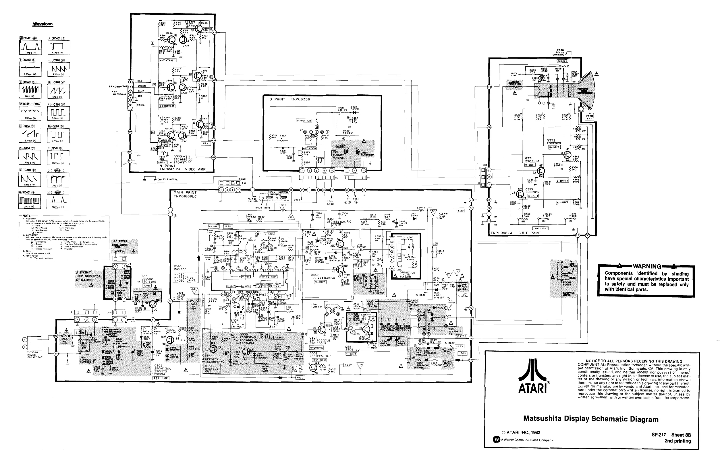
This page is a drawing, shown as the original scan.
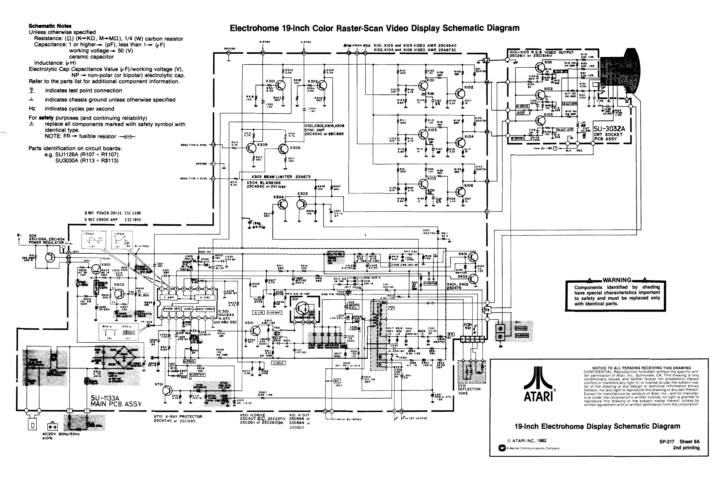
Schematic Notes
Unless otherwise specified Electrohome 19-inch Color Raster-Scan Video Display Schematic Diagram Resistance: (Q) (K--KQ, M--M®@), 1/4 (W) carbon resistor wane uavne Capacitance: 1 or higher-» (pF), less than 1—> (yF) | Blug oncen RED XI01.XI03 and XIOS VIDEO AMP, 2SC454C working voltage -» 50 (V) noun X102.X104 and _XI06 VIDEO AMP. 2SA673C EOI ceramic capacitor re 28261! or a Inductance: (H) Electrolytic Cap: Capacitance Value (v F)/working voltage (V), NP — non-polar (or bipolar) electrolytic cap. Refer to the parts list for additional component information. Q indicates test point connection oh indicates chassis ground unless otherwise specified roe Hz indicates cycles per second For safety purposes (and continuing reliability)
| a | replace all components marked with safety symbol with | X301,X302,X308,x306 | | |
| identical type. | IsyNc AMP | ISU-3032A | |
| NOTE: FR- fusible resistor —ex— | a | ircs a |
Parts identification on circuit boards: meenrwennere [tL e.g. SU1126A (R107 = R1107) SU3030A (R113 = R3113) wns
seen‘ Tivt eerie: X303 BEAM LIMITER 2SA673 wis | X304 BLANKING 2SC4S4C on 28C/egs
X901 POWER DRIVE 2SC 2688 ‘me X 902 ERROR AMP = 2SC 1890 a —————— oss a x04 = 2SCIOGA, 2SC1454 Powt LATOR fER REGULATC
ae Me noe Components identified by shading have special characteristics important et neio re be cur to safety and must be replaced only with identical parts.
ree byor DEFLECTION YOKE, confers or transfers any right in, or license to use, the subject mat. ter of the drawing or any design or technical information shown NOTICE TO ALL PERSONS RECEIVING THIS DRAWING CONFIDENTIAL: Reproduction forbidden without the specific writ ten permission of Atari, Inc., Sunnyvale, CA. This drawing is only conditionally issued, and neither receipt nor possession thereot
thereon, nor any right to reproduce this drawing or any part thereot, Except for manufacture by vendors of Atari, Inc., and for manufac: ture under the corporation's written license, no right is granted to reproduce this drawing or the subject matter thereof, unless by written agreement with or written permission from the corporation. SU-1133A MAIN PCB ASSY
r 7 wre cathY RROTECTOR Beis? OO, 2sces7iv 280808 er ce tu: sien he nr weaten or 2SCI685 2SC26ll or ZSC2610BK 2SD869 or . ; . 280820 19-Inch Electrohome Display Schematic Diagram ACI20V 60H2/50H2 210% © ATARI INC., 1982 SP-217 Sheet 9A Qo visvver Communications Company 2nd printing
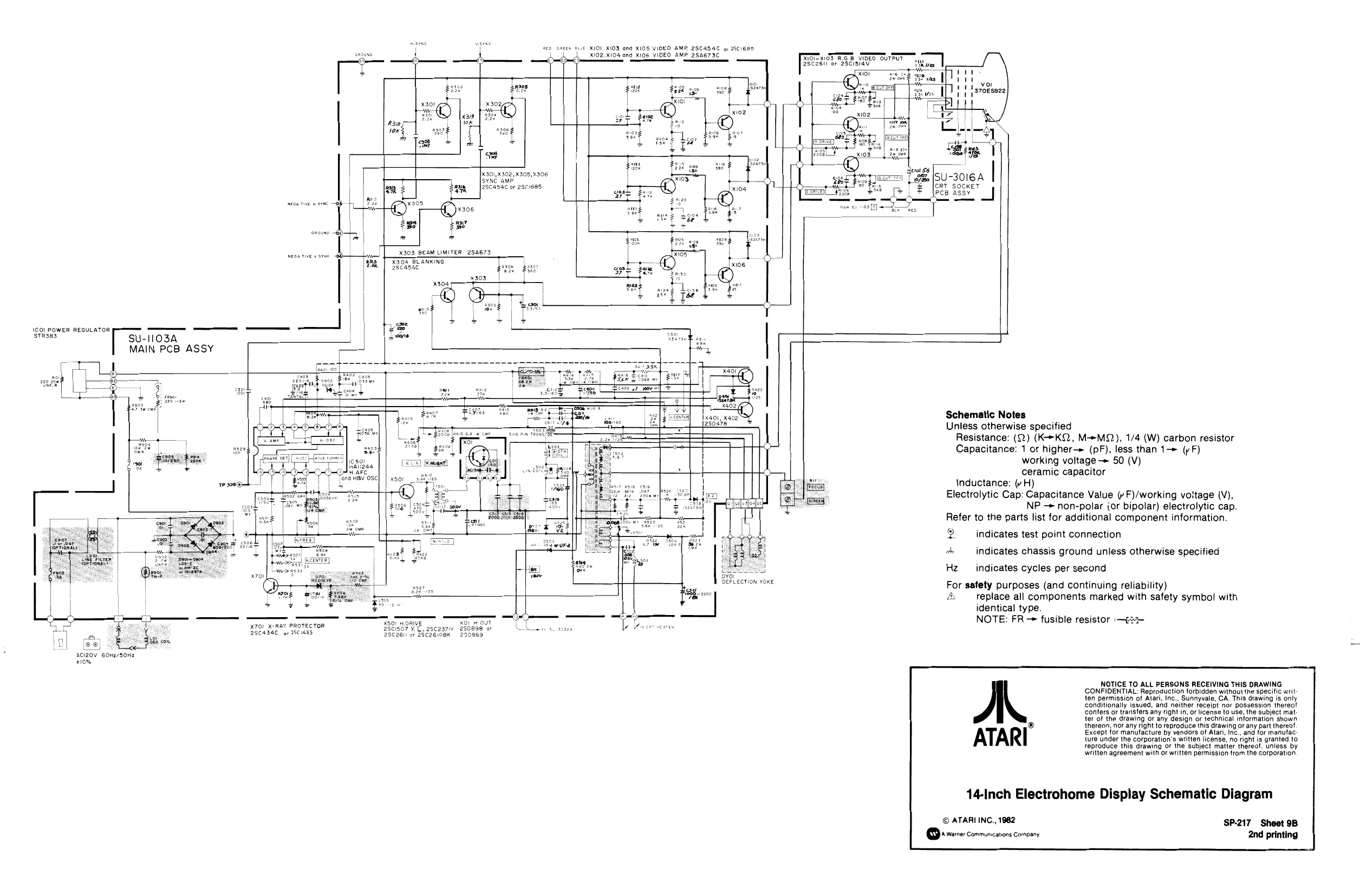
This page is a drawing, shown as the original scan.
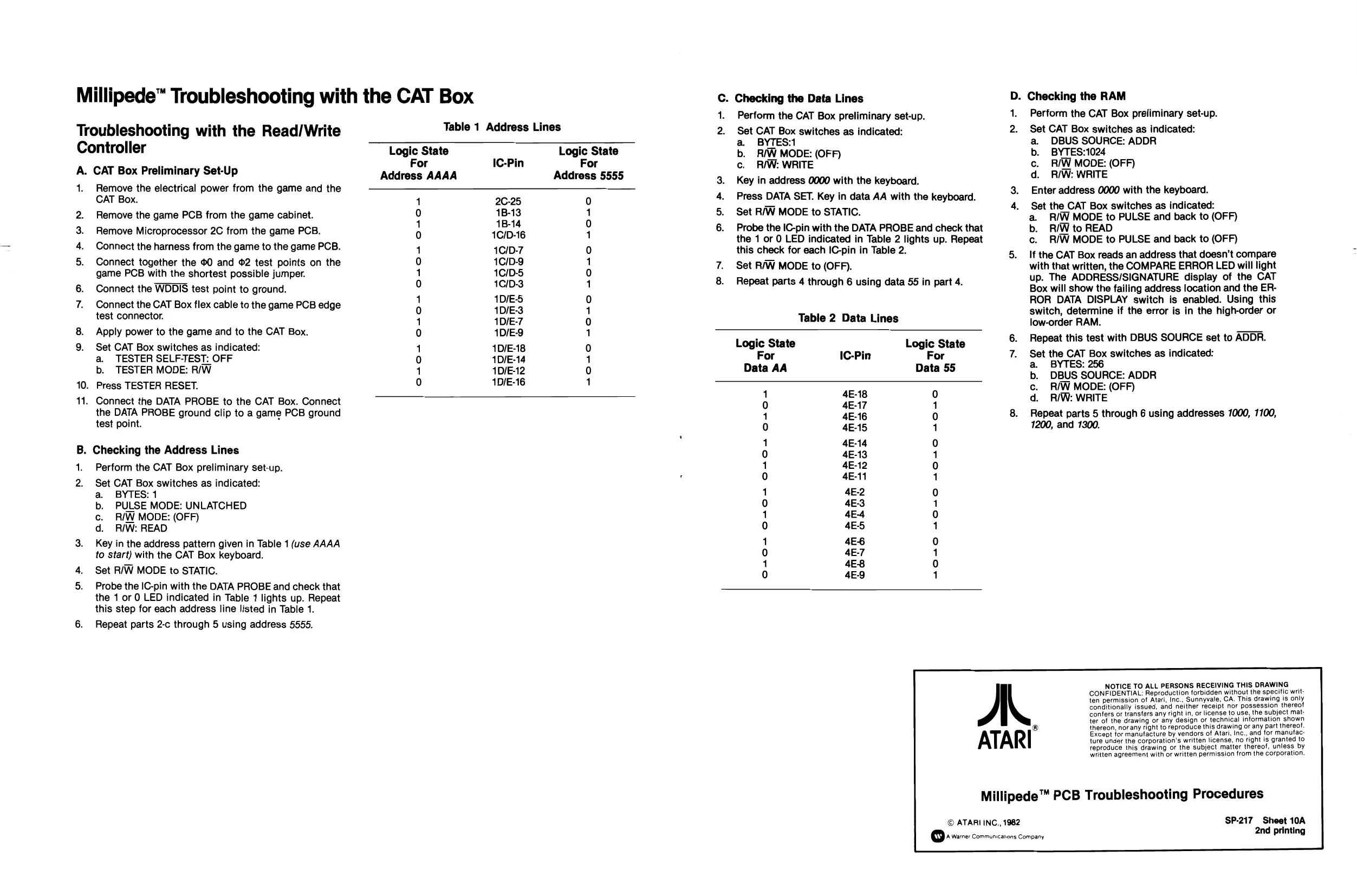
| Millipede™ Troubleshooting with the CAT Box | ©. Checking the Data Lines | D. Checking the RAM | |||||
| 1. | Perform the CAT Box preliminary set-up. | Perform the CAT Box preliminary set-up. | |||||
| Troubleshooting with the Read/Write | Table 1 Address Lines | 2. | Set CAT Box switches as indicated: | 2. | Set CAT Box switches as indicated: | ||
| Controlle | - | a | BYTES: | a. | DBUS SOURCE: ADDR | ||
| ontrolier | Logic State | Logic State | b. | RAW MODE: (OFF) | b. | BYTES: 1024 | |
| For | IC-Pin | For | c. | RW: WRITE | c. | R/W | MODE: (OFF) |
A. CAT Box Preliminary Set-U " . W:
| . ry | P | Address AAAA | Address 5555 | 3. | Key in address 0000 with the keyboard. | @. | RIW: WRITE | ||
| 1. | Remove the electrical power from the game and the | 4. | Press DATA SET. Key in data AA with the keyboard | 3. | Enter address 0000 with the keyboard. | ||||
| CAT ESE: | ; | 7 | 2¢-25 | 9 | 5. | Set RW MODE to STATIC. | . | 4, | Set the CAT Box switches as indicated: |
| 2. | Remove the game PCB from the game cabinet. | 0 | 1B-13 | 1 | ahs | 7 | 7 | a. | R/W MODE to PULSE and back to (OFF) |
| 3. | Remove Microprocessor 2C from the game PCB. | i | Aas | 0 | 6. | Probe the IC-pin with the DATA PROBE and check that | b. | RIW to READ | |
| C | 0 | 10/D-16 | 1 | the 1 or 0 LED indicated in Table 2 lights up. Repeat | c. | R/W MODE to PULSE and back to (OFF) | |||
| 4. | Connect the harness from the game to the game PCB. | 1 | 4C/D-7 | 0 | this check for each IC-pin in Table 2. | 5. | If the CAT Box reads an address that doesn't compare | ||
| 5. | Connect together the 0 and ©2 test points on the | 0 | 10/D-9 | 1 | 7. | Set RAW MODE to (OFF). | with that written, the COMPARE ERROR LED will light | ||
| game PCB with the shortest possible jumper. | 3 | {ois | ° | 8. | Repeat parts 4 through 6 using data 55 in part 4 | up. The ADDRESS/SIGNATURE display of the CAT | |||
| 6. | Connect the WDDIS test point to ground. | : | . | Box will show the failing address location and the ER- | |||||
| 1 | 1D/E-5 | 0 | ROR DATA DISPLAY switch is enabled. Using this | ||||||
| 7 | Connect the GAT Box flex cable te the game PCB edge | 0 | 1DIE3 | 1 | switch, determine if the error is in the high-order or | ||||
| Rest commieciOk | 1 | 1DIE7 | 0 | Table 2 Data Lines | low-order RAM. | ||||
| 8. | Apply power to the game and to the CAT Box. | 0 | 1D/E-9 | 1 | ii | ADDR. | |||
| 9. | Set CAT Box switches as indicated: | 1 | 1Dre18 | 0 | Logic State | Logic State | 6. | Repeat this test with DBUS SOURCE set to ADDR. | |
| “a, | TESTER SELF-TEST: OFF | , | For | IC-Pin | For | 7. | Set the CAT Box switches as indicated: | ||
| ¥ | “TEST: | | 0 | 1DIE-14 | 1 | a. | BYTES: 256 |
b. TESTER MODE: RIW 1 1DIEA2 0 Data AA Data 55 b. DBUS SOURCE: ADDR
| 10. Press TESTER RESET. | 0 | 1DIE-AG | 1 | 1 | 1E18 | 0 | c. | RIW MODE: (OFF) |
| 11. Connect the DATA PROBE to the CAT Box. Connect | 0 | 46-17 | 1 | d. | RAW: WRITE | |||
| the DATA PROBE ground clip to a game PCB ground | 1 | 4E-16 | 0 | 8. | Repeat parts 5 through 6 using addresses 1000, 1100, | |||
| test point. | 0 | 4E-15 | 1 | 1200, and 1300. | ||||
| B. Checking the Address Lines | : | ie | : |
1. Perform the CAT Box preliminary set-up. 0 ae 0
| 2. | Set CAT Box switches as indicated: | " | 1 | |
| a. | BYTES: 1 | 1 | 4E2 | o |
| b. | PULSE MODE: UNLATCHED | 0 | 4E3 | 1 |
| c. | R/W MODE: (OFF) | 1 | 4E-4 | 0 |
| d. | RIW: READ | 0 | 4eE5 | 1 |
| 3. | Key in the address pattern given in Table 1 (use AAAA | 1 | 4E6 | 0 |
| to start) with the CAT Box keyboard. | ° | ‘ta | } |
4. Set RIW MODE to STATIC. 0 aE8 1
- Probe the IC-pin with the DATA PROBE and check that the 1 or 0 LED indicated in Table 1 lights up. Repeat this step for each address line listed in Table 1.
- Repeat parts 2-c through 5 using address 5555.
NOTICE TO ALL PERSONS RECEIVING THIS DRAWING CONFIDENTIAL: Reproduction forbidden without the specitic writ ten permission of Atari, Inc., Sunnyvale, CA. This drawing is only conditionally issued, and neither receipt nor possession thereof confers or transters any right in, or license to use, the subject matter of the drawing or any design or technical information shown ® thereon, norany right to reproduce this drawing or any part thereof. Except for manufacture by vendors of Atari, Inc., and for manufac: ture under the corporation's written license, no right is granted to reproduce this drawing or the subject matter thereof, unless by written agreement with or written permission from the corporation.
Millipede™ PCB Troubleshooting Procedures
© ATARI INC., 1982 SP-217 Sheet 10A + Ware: communicarons Company 2nd printing
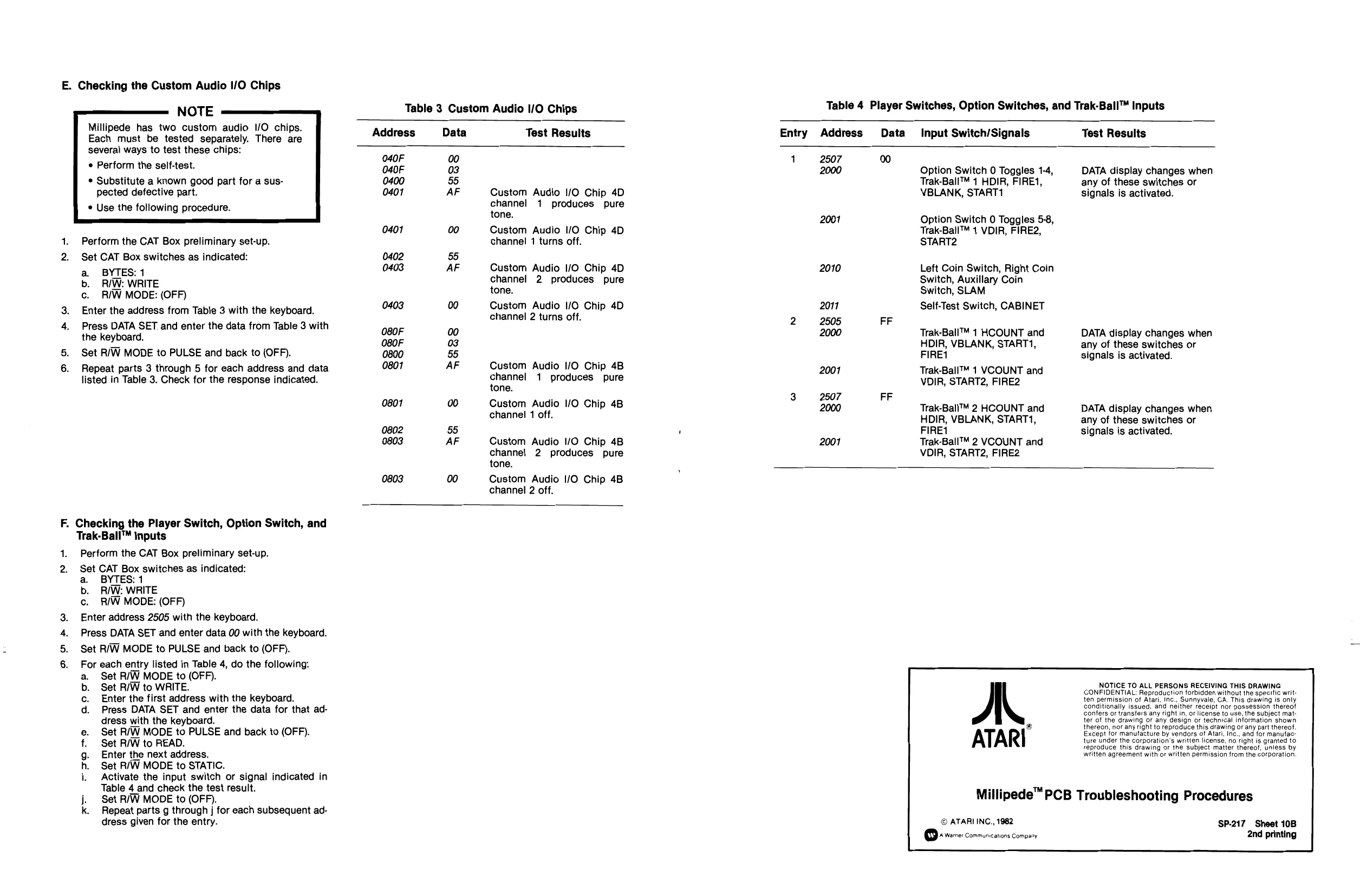
E. Checking the Custom Audio I/O Chips
F.
Paro
Perform the CAT Box preliminary set-up. Set CAT Box switches as indicated: a BYTES: 1 b. IW: WRITE c. R/W MODE: (OFF) Enter the address from Table 3 with the keyboard. Press DATA SET and enter the data from Table 3 with the keyboard. Set R/W MODE to PULSE and back to (OFF). Repeat parts 3 through 5 for each address and data listed in Table 3. Check for the response indicated.
Checking the Player Switch, Option Switch, and Trak-Ball™ inputs Perform the CAT Box preliminary set-up. Set CAT Box switches as indicated: a. BYTES: 1 b. RW: WRITE c. R/W MODE: (OFF) Enter address 2505 with the keyboard. Press DATA SET and enter data 00 with the keyboard. Set R/W MODE to PULSE and back to (OFF). For each entry listed in Table 4, do the following: Set R/W MODE to (OFF). Set R/W to WRITE. Enter the first address with the keyboard. Press DATA SET and enter the data for that address with the keyboard. Set R/W MODE to PULSE and back to (OFF). Set R/W to READ. Enter the next address. Set R/W MODE to STATIC. Activate the input switch or signal indicated in Table 4 and check the test result. Set R/W MODE to (OFF). Repeat parts g through j for each subsequent address given for the entry. aogoe
rsame
ao Table 3 Custom Audio |/O Chips
Address Data Test Results
O40F 00 040F 03 0400 55
| 0401 | AF | Custom Audio I/O Chip 4D |
channel 1 produces pure tone.
| 0401 | 00 | Custom Audio I/O Chip 4D |
channel 1 turns off. 0402 55
| 0403 | AF | Custom Audio I/O Chip 4D |
channel 2 produces pure tone.
| 0403 | 00 | Custom Audio 1/0 Chip 4D |
channel 2 turns off. O80F 00 O80F 03 0800 55
| 0801 | AF | Custom Audio I/O Chip 4B |
channel 1 produces pure tone.
| 0801 | 00 | Custom Audio I/O Chip 4B |
channel 1 off. 0802 55
| 0803 | AF | Custom Audio 1/0 Chip 4B |
channel 2 produces pure tone.
| 0803 | 00 | Custom Audio 1/0 Chip 4B |
channel 2 off. Table 4 Player Switches, Option Switches, and Trak-Ball™ Inputs
| Entry | Address | Data _ Input Switch/Signals | Test Results |
| 1 | 2507 | 00 | |
| 2000 | Option Switch 0 Toggles 1-4, | DATA display changes when |
Trak-Ball™ 1 HDIR, FIRE1, any of these switches or VBLANK, START1 signals is activated.
2001 Option Switch 0 Toggles 5-8, Trak-Ball™ 1 VDIR, FIRE2, START2
2010 Left Coin Switch, Right Coin Switch, Auxillary Coin Switch, SLAM 2017 Self-Test Switch, CABINET
| 2 | 2505 | Fr |
| 2000 | Trak-Ball™ 1 HCOUNT and | DATA display changes when |
HDIR, VBLANK, START1, any of these switches or FIRE1 signals is activated. 2001 Trak-Ball™ 1 VCOUNT and VDIR, START2, FIRE2
| 3 | 2507 | FF |
| 2000 | Trak-Ball™ 2 HCOUNT and | DATA display changes when |
HDIR, VBLANK, START1, any of these switches or FIRE1 signals is activated. 2001 Trak-Ball™ 2 VCOUNT and VDIR, START2, FIRE2
A,
ATARI
NOTICE TO ALL PERSONS RECEIVING THIS DRAWING ‘CONFIDENTIAL: Reproduction forbidder. without the specific written permission of Atari, Inc., Sunnyvale, CA. This drawing is only conditionally issued, and neither receipt nor possession thereo!
Confers or transfers any right in, or license to use, the subject mat
ter of the drawing or any design or technical information shown thereon, nor any tight to reproduce this drawing or any part thereof. Except lor manufacture by vendors of Atari Inc., and for manufacture Under the corporation's written license, no right is granted to, reproduce this drawing or the subject matier thereof, unless by written agreement with or written permission from the corporation.
Millipede™ PCB Troubleshooting Procedures
© ATARI INC., 1982 SP-217 Sheet 10B
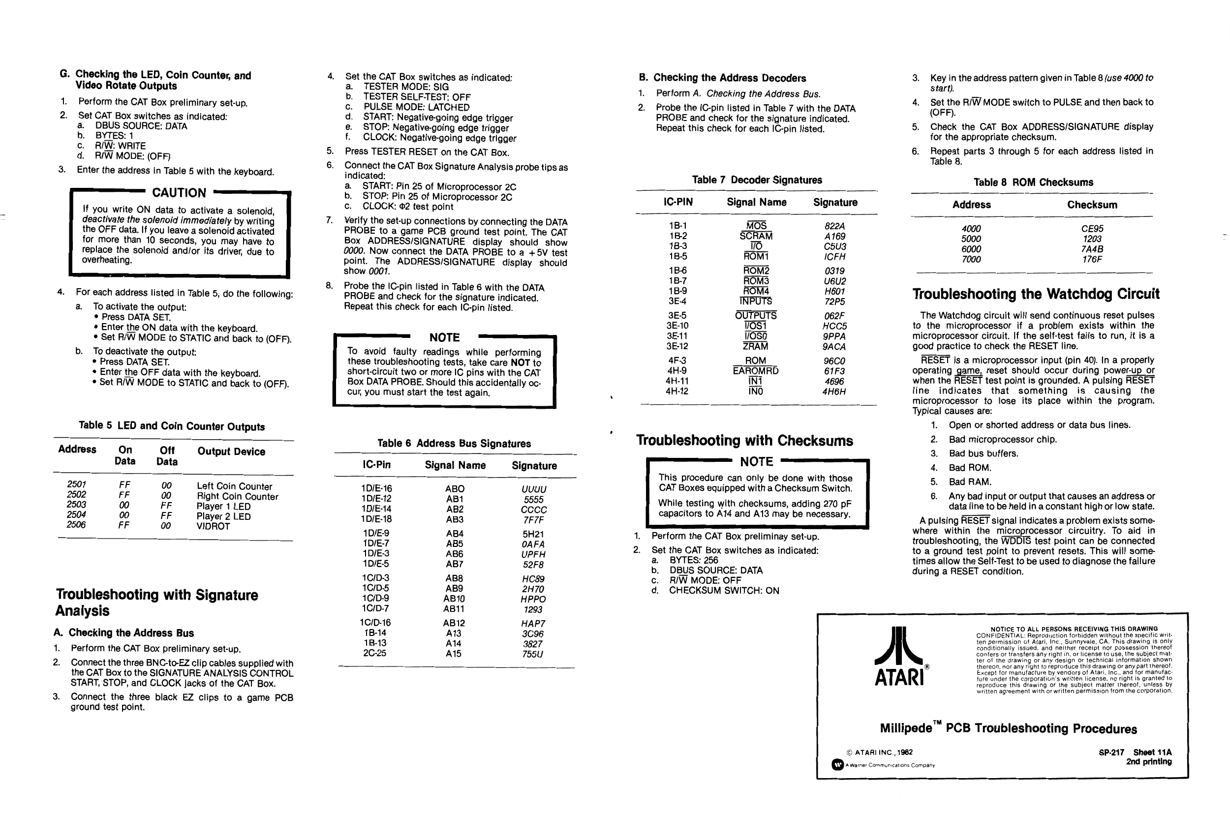
4. . Checking the LED, Coin Counter, and Video Rotate Outputs Perform the CAT Box preliminary set-up. Set CAT Box switches as indicated: a. DBUS SOURCE: DATA b. BYTES: 1 c. IW: WRITE d. R/W MODE: (OFF) Enter the address in Table 5 with the keyboard.
For each address listed in Table 5, do the following: a. To activate the output: © Press DATA SET,
- Enter the ON data with the keyboard.
- Set R/W MODE to STATIC and back to (OFF). b. To deactivate the output:
- Press DATA SET.
- Enter the OFF data with the keyboard.
- Set R/W MODE to STATIC and back to (OFF).
Table 5 LED and Coin Counter Outputs
Address On Oft
Output Device Set the CAT Box switches as indicated: TESTER MODE: SIG TESTER SELF-TEST: OFF PULSE MODE: LATCHED START: Negative-going edge trigger STOP: Negative-going edge trigger . CLOCK: Negative-going edge trigger Press TESTER RESET on the CAT Box. Connect the CAT Box Signature Analysis probe tips as indicated: a. START: Pin 25 of Microprocessor 2C b, STOP: Pin 25 of Microprocessor 2C c. CLOCK: 2 test point Verify the set-up connections by connecting the DATA PROBE to a game PCB ground test point. The CAT Box ADDRESS/SIGNATURE display should show 9000. Now connect the DATA PROBE to a +5V test point. The ADDRESS/SIGNATURE display should show 0001. Probe the IC-pin listed in Table 6 with the DATA PROBE and check for the signature indicated. Repeat this check for each IC-pin listed. rpaccp
Table 6 Address Bus Signatures
Data Data IC-Pin Signal Name Signature
| 2507 | FF | 00 | Left Coin Counter | 1D/E-16 | ABO | Uuuu |
| 2502 | FF | 00 | Right Coin Counter | 1D/E-12 | ABI | 5555 |
2503 00 FF Player 1 LED 4DIEA4 ABZ cccc
| pod | 00 | Fr | Player 2 LED | 1D/E-18 | AB3 | 7F7F |
| ee | are: | 1DE9 | AB4 | sH2t | ||
| 1D/E-7 | ABS | OAFA | ||||
| 1D/E-3 | AB6 | UPFH | ||||
| 1D/E-5 | AB? | 52F8 | ||||
| 1C/D-3 | AB8 | HC89 | ||||
| . | ., | 7 | 1C/D-5 | ABS | 2H70 | |
| Troubleshooting with Signature | 10/D-9 | ABIO | HPPO | |||
| Analysis | 1C/D-7 | ABII | 1293 | |||
| 1C/D-16 | ABI2 | HAP7 | ||||
| A. Checking the Address Bus | 1B-14 | At | 3C96 | |||
| a | 1B-13 | A14 | 3827 | |||
| 1. | Perform the CAT Box preliminary set-up. | 20-25 | AS | 755U |
- Connect the three BNC-to-EZ clip cables supplied with the CAT Box to the SIGNATURE ANALYSIS CONTROL START, STOP, and CLOCK jacks of the CAT Box.
- Connect the three black EZ clips to a game PCB ground test point. B. Checking the Address Decoders 3. Key in the address pattern given in Table 8 (use 4000 to Start).
- Perform A. Checking the Address Bus.
| . | he | MODE | switch to PULSE and then back to |
2. Probe the iC-pin listed in Table 7 with the DATA ain: MORE euttehita
PROBE and check for the signature indicated. i : Repeat this check for each Ie-in listed. 5. Check the CAT Box ADDRESS/SIGNATURE display for the appropriate checksum.
- Repeat parts 3 through 5 for each address listed in Table 8.
Table 7 Decoder Signatures Table 8 ROM Checksums
IC-PIN Signal Name Signature Address Checksum
| 1BA | MOS | 8224 | 4000 | CE95 | |||
| 182 | SCRAM | A169 | 5000 | 1208 | |||
| 183 | lO | c5u3 | 6000 | 7A4B | |||
| 1B5 | ROMi | ICFH | 7000 | 176F | |||
| 1B6 | ROM2 | 0319 | |||||
| 1B-7 | ROMS | u6u2 | he | W. | hd | Ci | it |
| Hes | fom | 4601 | ing | t | atc! | ircui | |
| pes | TaPUTS | pil | Troubleshooting | the | log | ||
| 3E-5 | OUTPUTS | 062F | The Watchdog circuit will send continuous reset pulses |
3E-10 VOS1 HCC5 to the microprocessor if a problem exists within the
| 3E-11 | VOse | 9PPA | microprocessor circuit. If the self-test fails to run, itis a | ||||
| 3E12 | ZRAM | 9ACA | good practice to check the RESET line. | ||||
| 4F-3 | ROM | 96CO | RESET is a microprocessor input (pin 40). In a properly | ||||
| 4H-9 | EAROMRD | 61F3 | operating | game, reset should occur during power-up | or | ||
| 4H-11 | INT | 4696 | when the RESET test point is grounded. A pulsing RESE | ||||
| 4H-12 | INO | 4H6H | line | indicates that | something | is causing | the |
Troubleshooting with Checksums
- Perform the CAT Box preliminay set-up.
- Set the CAT Box switches as indicated: a. BYTES: 256 b. DBUS SOURCE: DATA c. R/W MODE: OFF d. CHECKSUM SWITCH: ON microprocessor to lose its place within the program. Typical causes are: 1.
Switch.
270 pF essary. 2ARON Open or shorted address or data bus lines. Bad microprocessor chip. Bad bus buffers. Bad ROM. Bad RAM. Any bad input or output that causes an address or data [ine to be held in a constant high or low state. A pulsing RESET signal indicates a problem exists somewhere within the microprocessor circuitry. To aid in troubleshooting, the DIS test point can be connected to a ground test point to prevent resets. This wil! sometimes allow the Self-Test to be used to diagnose the failure during a RESET condition.
ATARI NOTICE TO ALL PERSONS RECEIVING THIS DRAWING CONFIDENTIAL: Reproduction forbidden without the specific writ. ten permission of Atari, Inc., Sunnyvale, CA. This drawing is only conditionally issued, and nelther receipt nor possession thereof confers or transters any right in, or license to use, the subject matter of the drawing or any design or technical information shown thereon, nor any right to reproduce this drawing or any part thereof, Except for manufacture by vendors of Atari, Inc., and for manufac: ture under the corporation's written license, no right is granted to reproduce this drawing or the subject matter thereof, unless by written agreement with or written permission from the corporation.
Millipede™ PCB Troubleshooting Procedures
© ATAAIINC., 1982 SP-217 Sheet 11A