Crystal Castles SP-241 2nd Printing
Crystal Castles (version 4) (Atari, 1983) · Schematic Package · 23 pages · 66 sections · original scan
This page is a drawing, shown as the original scan.
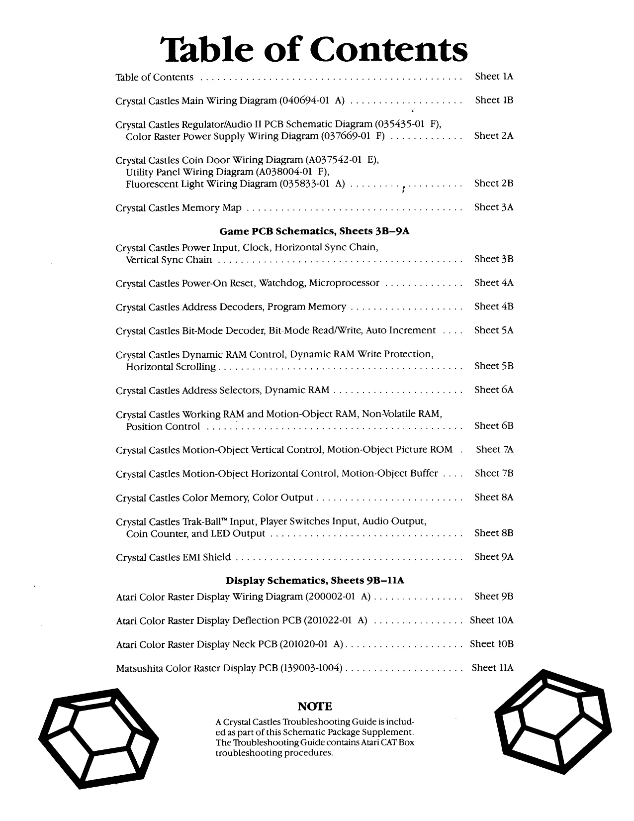
Table of Contents Table of Contents 6.2... eee ett Sheet 1A
Crystal Castles Main Wiring Diagram (040694-01 A) ............00 0.000 Sheet 1B
Crystal Castles Regulator/Audio II PCB Schematic Diagram (035435-01 F), Color Raster Power Supply Wiring Diagram (037669-01 F) ............. Sheet 2A
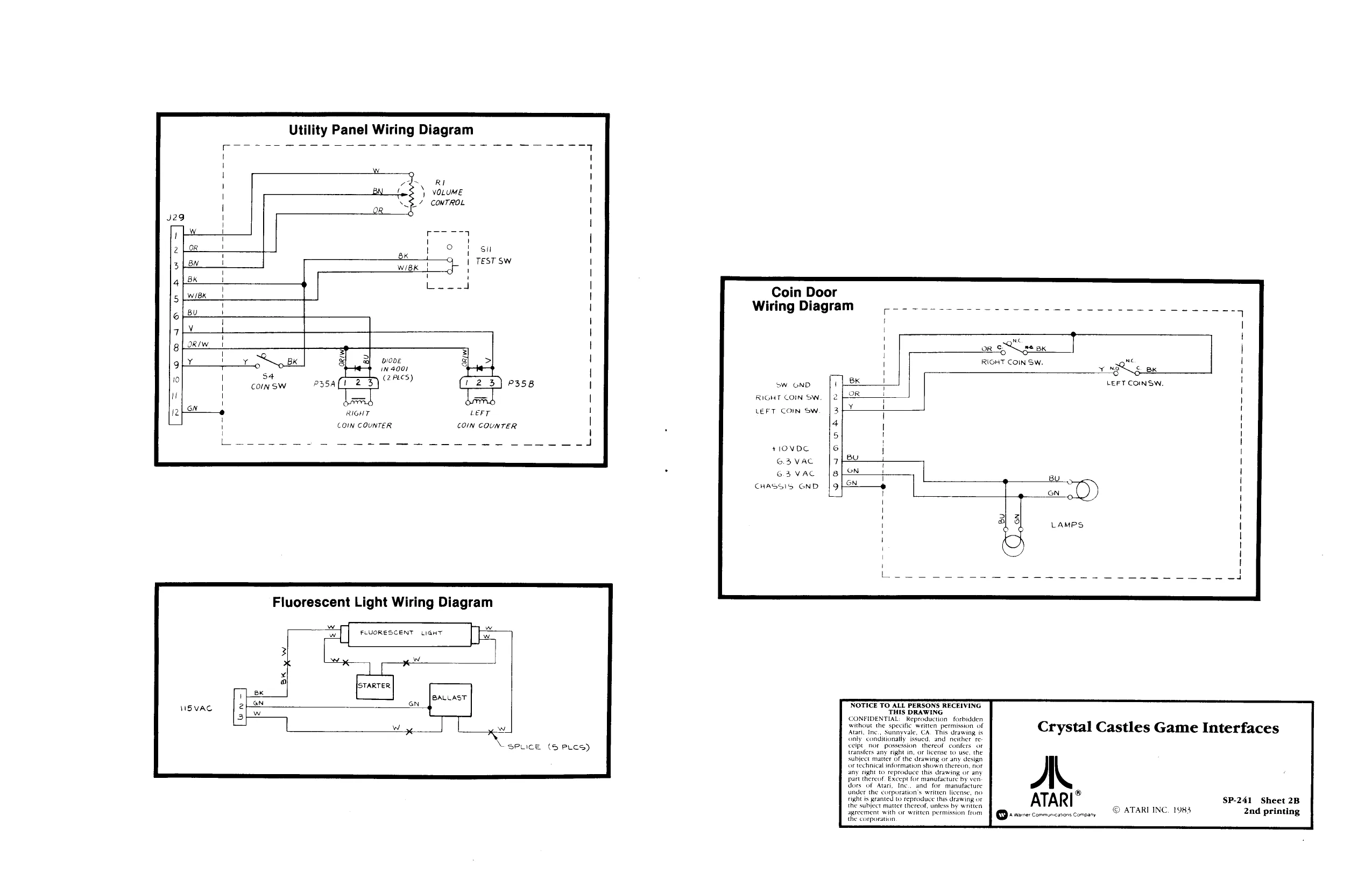
Crystal Castles Coin Door Wiring Diagram (A037542-01 E), Utility Panel Wiring Diagram (A038004-01 F), Fluorescent Light Wiring Diagram (035833-01 A) ......... processes Sheet 2B
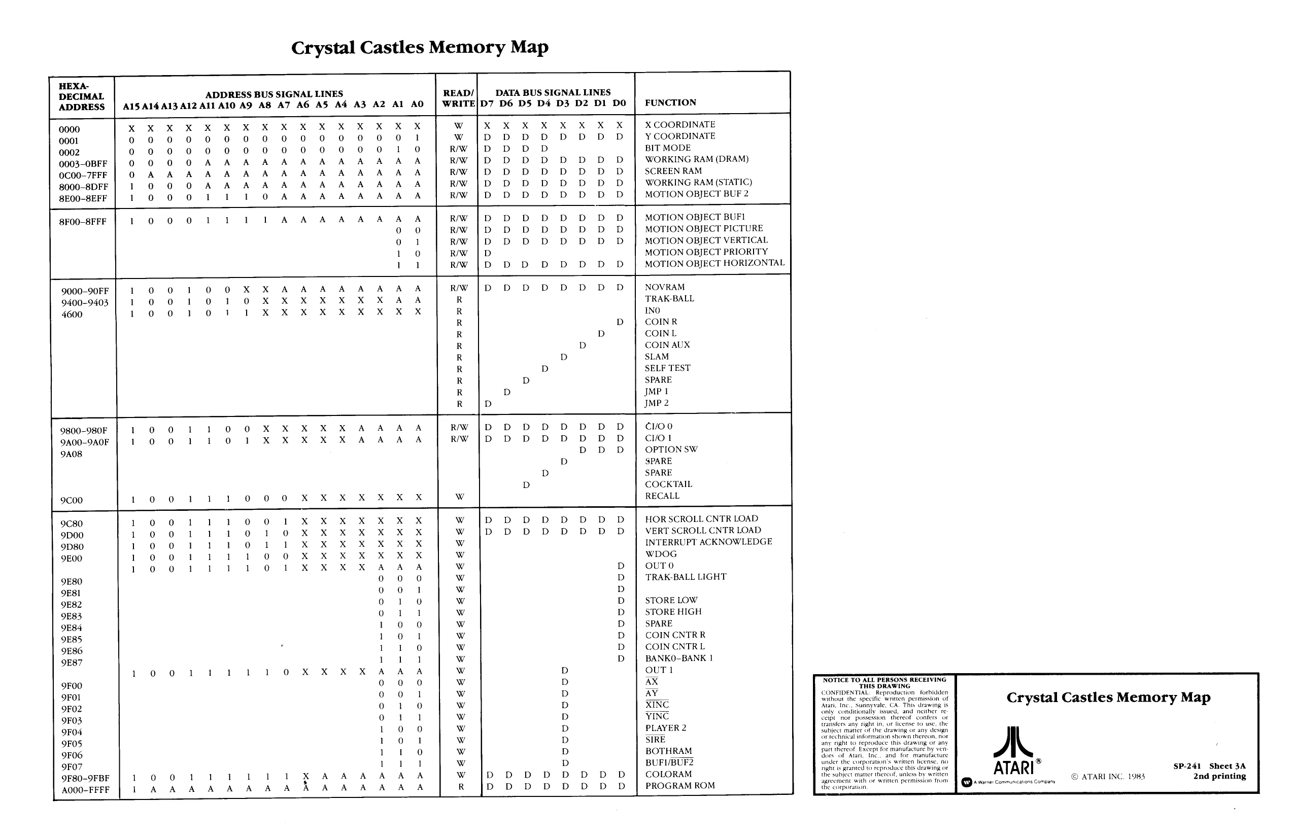
Crystal Castles Memory Map ......--- 2-02 e eee Sheet 3A
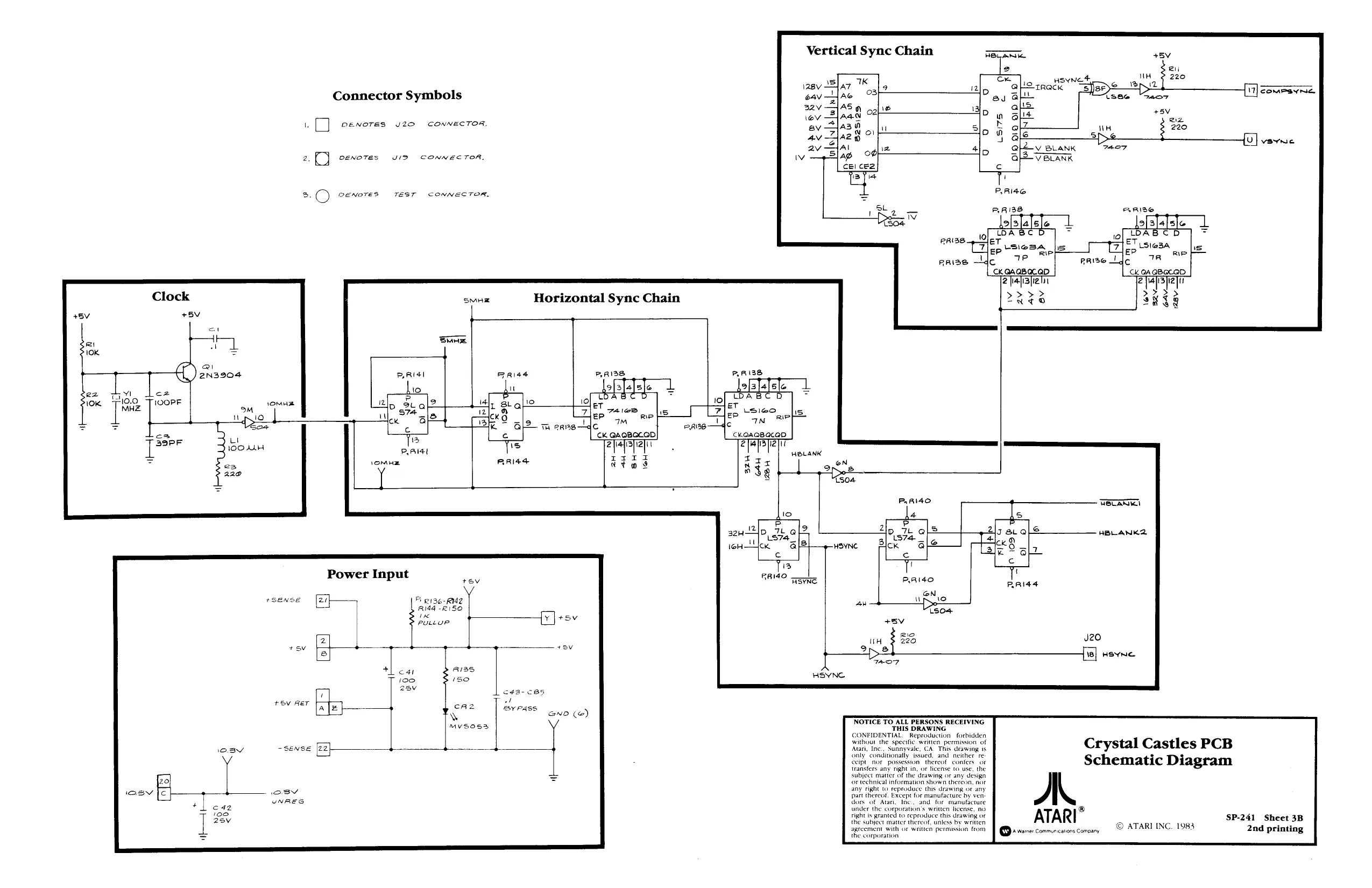
Game PCB Schematics, Sheets 3B-9A Crystal Castles Power Input, Clock, Horizontal Sync Chain, Vertical Sync Chain 20... eee Sheet 3B
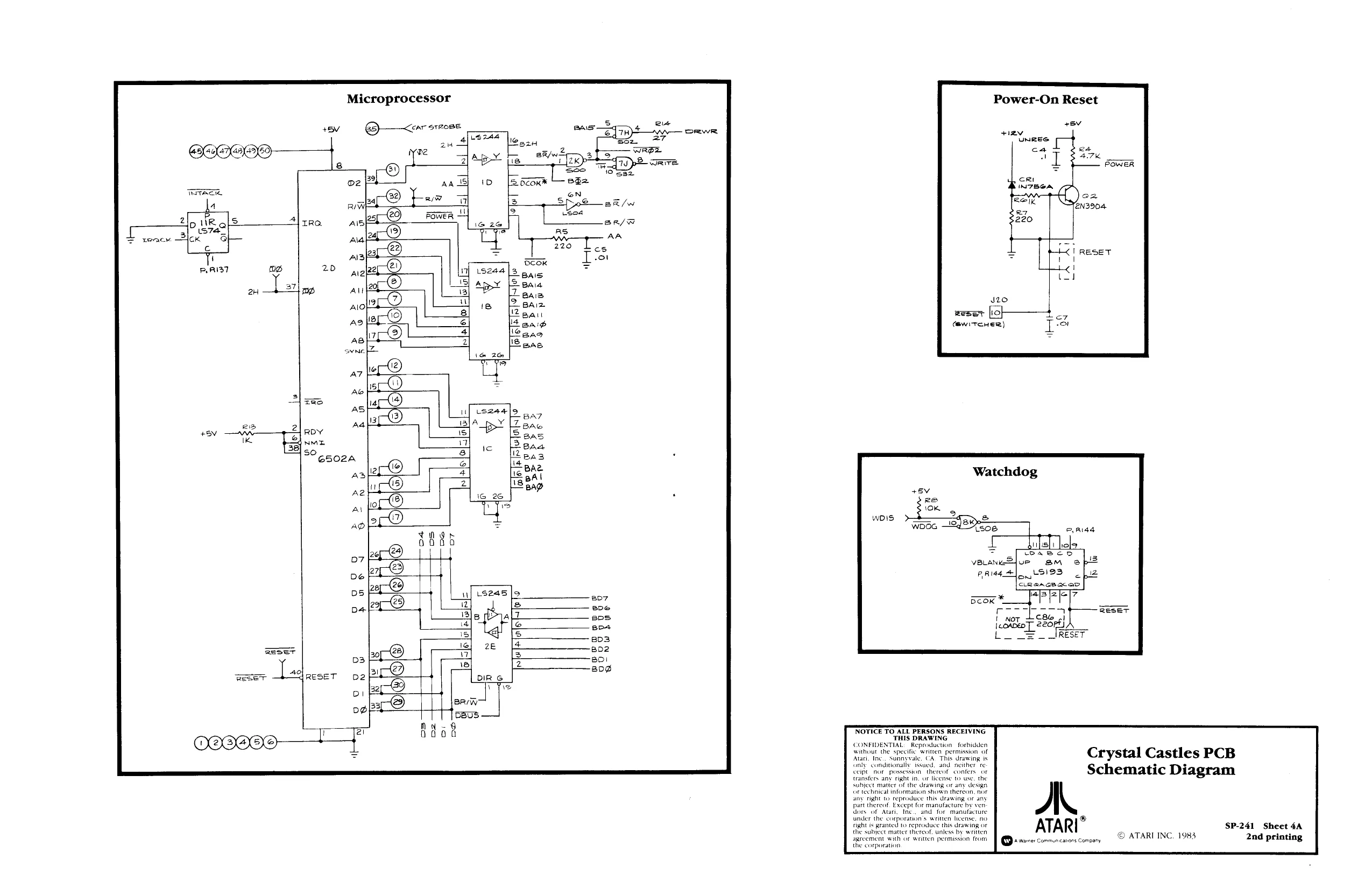
Crystal Castles Power-On Reset, Watchdog, Microprocessor .............. Sheet 4A.
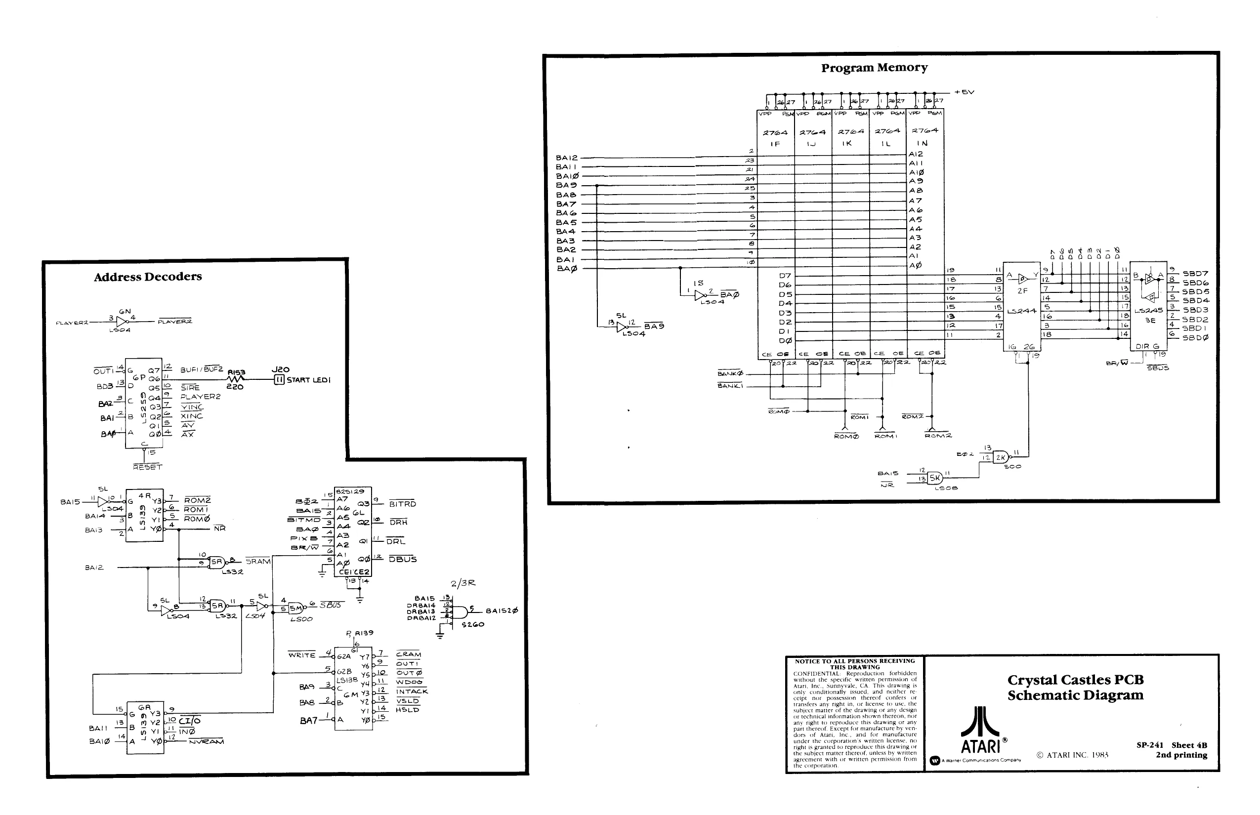
Crystal Castles Address Decoders, Program Memory .....-....-+ 00020005 Sheet 4B
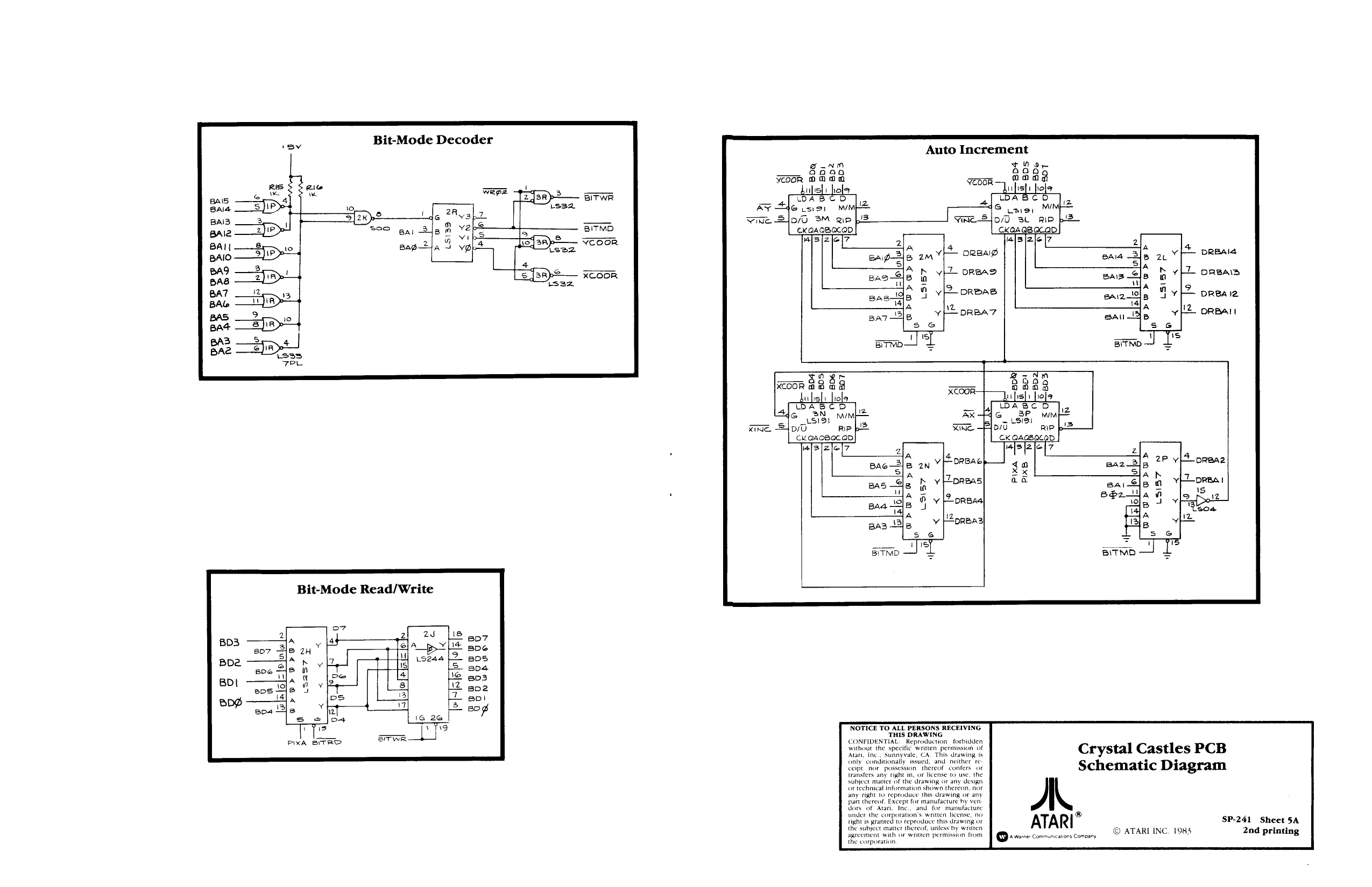
Crystal Castles Bit-Mode Decoder, Bit-Mode Read/Write, Auto Increment .... Sheet SA
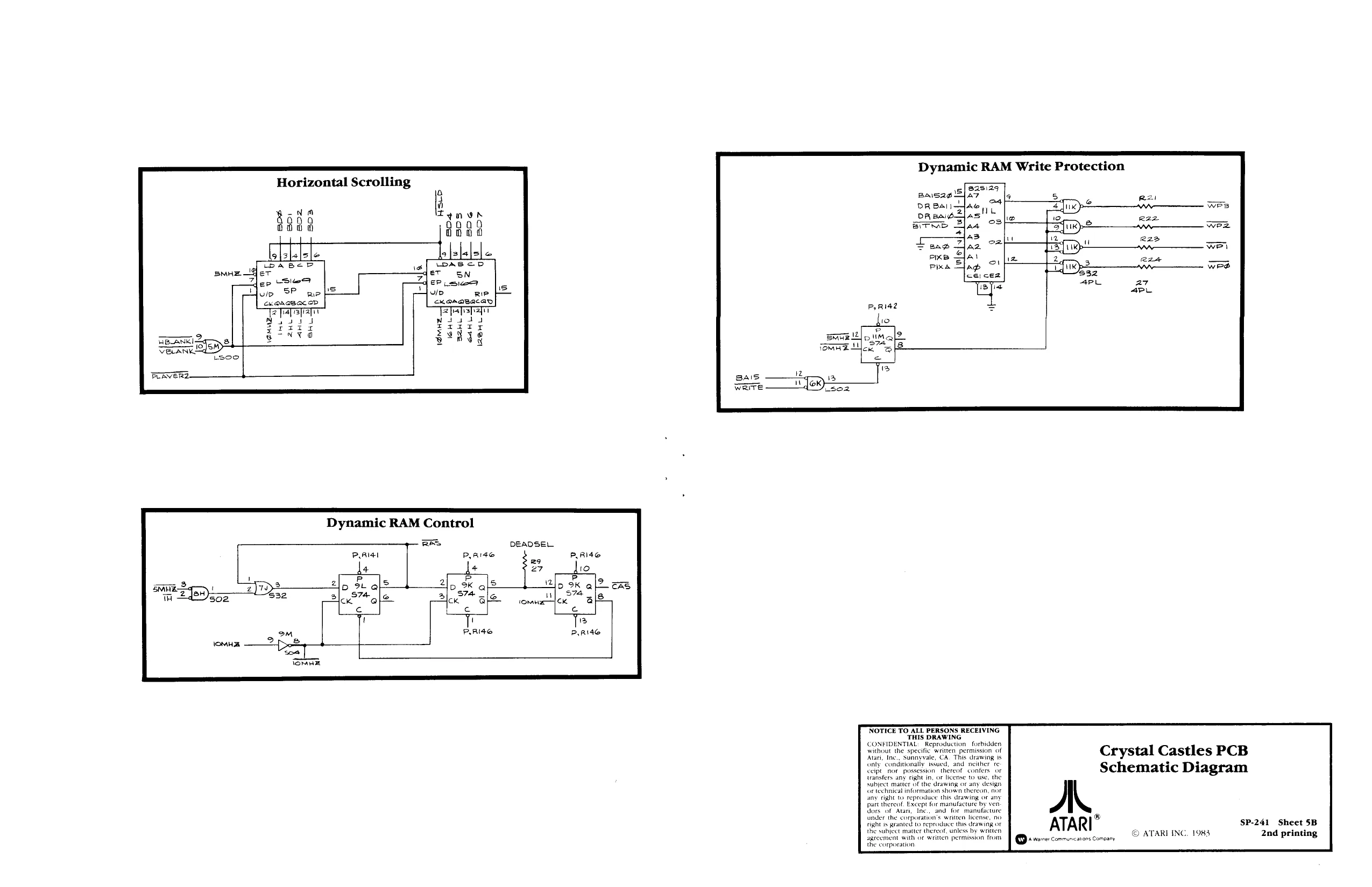
Crystal Castles Dynamic RAM Control, Dynamic RAM Write Protection, Horizontal Scrolling... 0.0... eee Sheet 5B
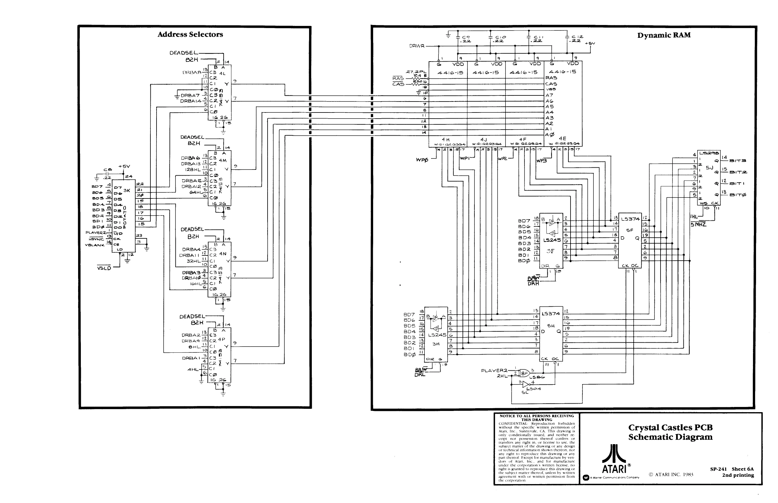
Crystal Castles Address Selectors, Dynamic RAM .. 0... 06. eee eee eee Sheet 6A
Crystal Castles Working RAM and Motion-Object RAM, NonVolatile RAM, Position Control 60... nee ee Sheet 6B
Crystal Castles Motion-Object Vertical Control, Motion-Object Picture ROM . Sheet 7A
Crystal Castles Motion-Object Horizontal Control, Motion-Object Buffer .... Sheet 7B
Crystal Castles Color Memory, Color Output... 2.6.0... 60. e eee eee Sheet 8A
Crystal Castles Trak-Ball™ Input, Player Switches Input, Audio Output, Coin Counter, and LED Output .. 0... eee Sheet 8B
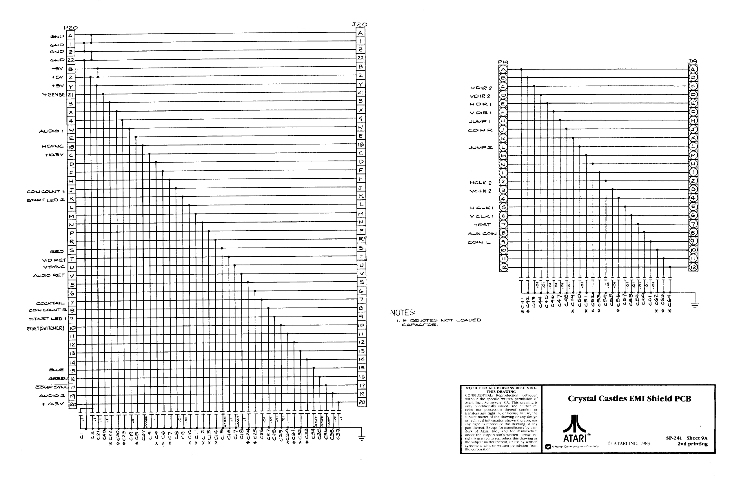
Crystal Castles EMI Shield... 02.0... Sheet 9A
Display Schematics, Sheets 9B-11A Atari Color Raster Display Wiring Diagram (200002-01 A)...........-.--- Sheet 9B
Atari Color Raster Display Deflection PCB (201022-01 A) ...........-.-05 Sheet 10A
Atari Color Raster Display Neck PCB (201020-01 A)...........0000000005 Sheet 10B
Matsushita Color Raster Display PCB (139003-1004)................20000- Sheet 11A
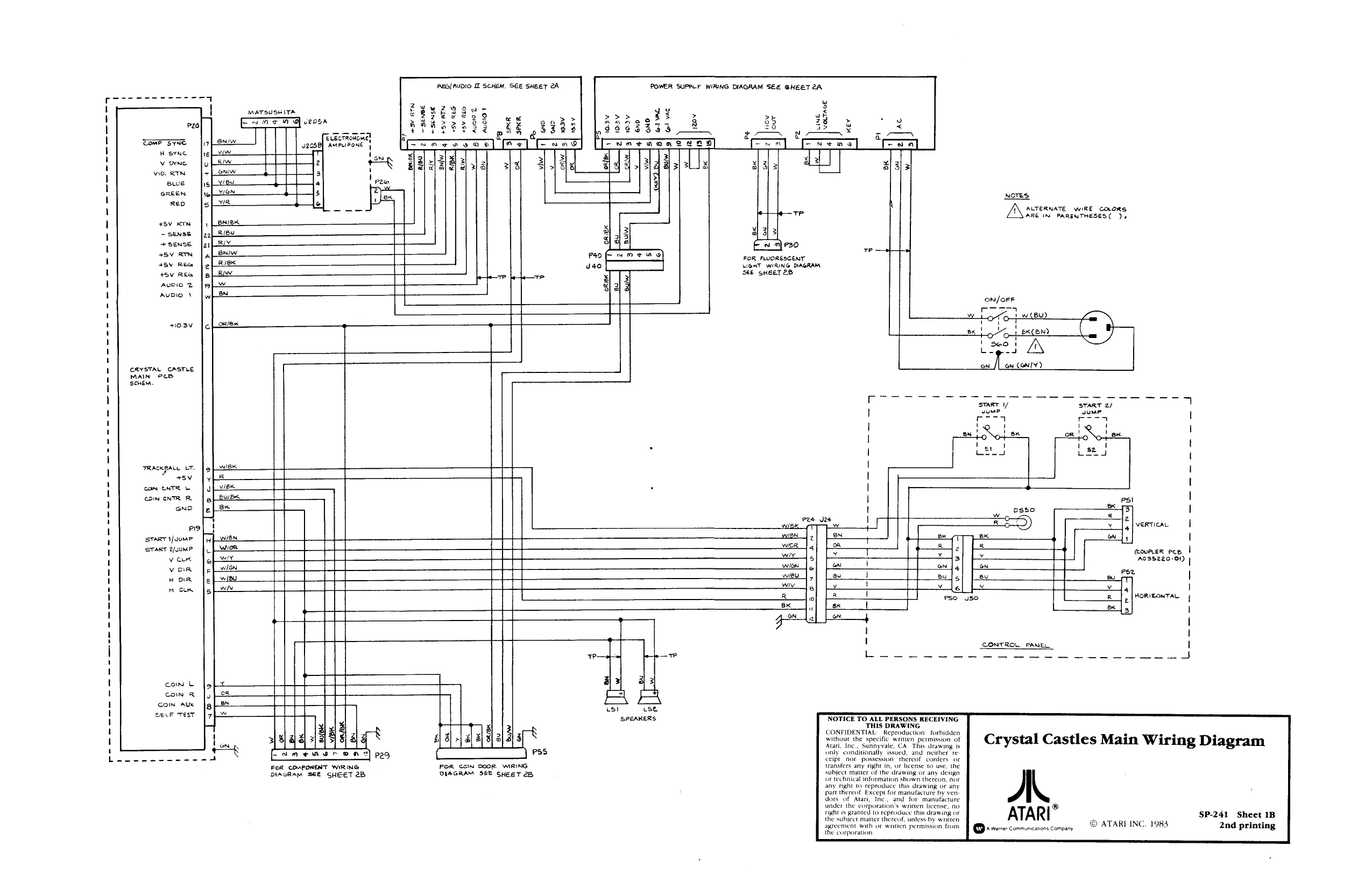
This page is a drawing, shown as the original scan.
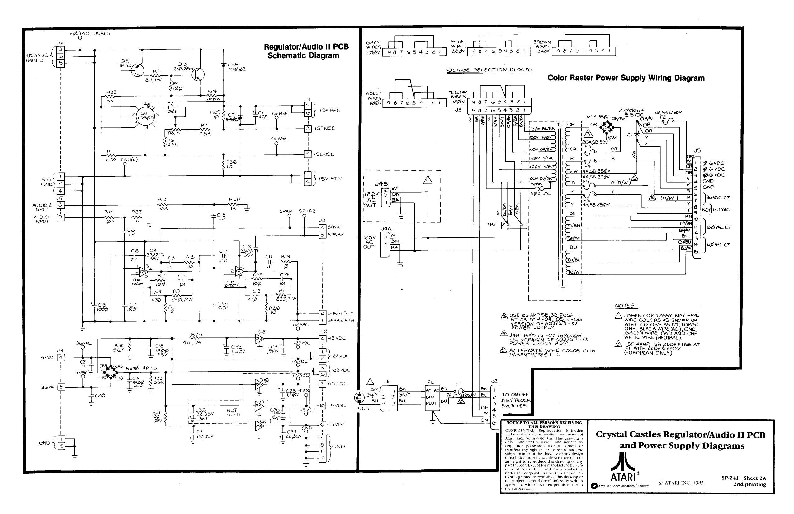
This page is a drawing, shown as the original scan.
This page is a drawing, shown as the original scan.
This page is a drawing, shown as the original scan.
This page is a drawing, shown as the original scan.
This page is a drawing, shown as the original scan.
This page is a drawing, shown as the original scan.
This page is a drawing, shown as the original scan.
This page is a drawing, shown as the original scan.
This page is a drawing, shown as the original scan.
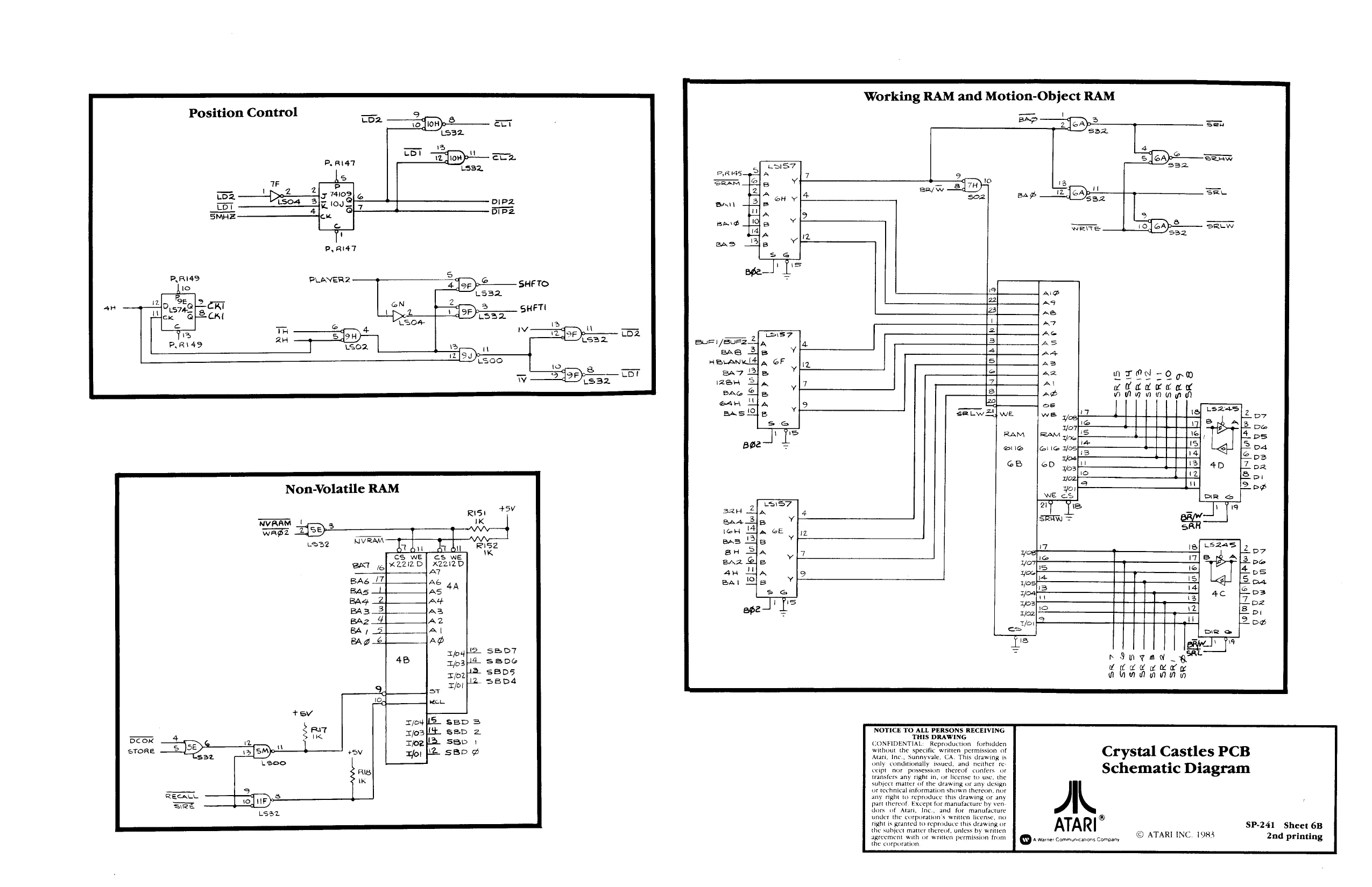
This page is a drawing, shown as the original scan.
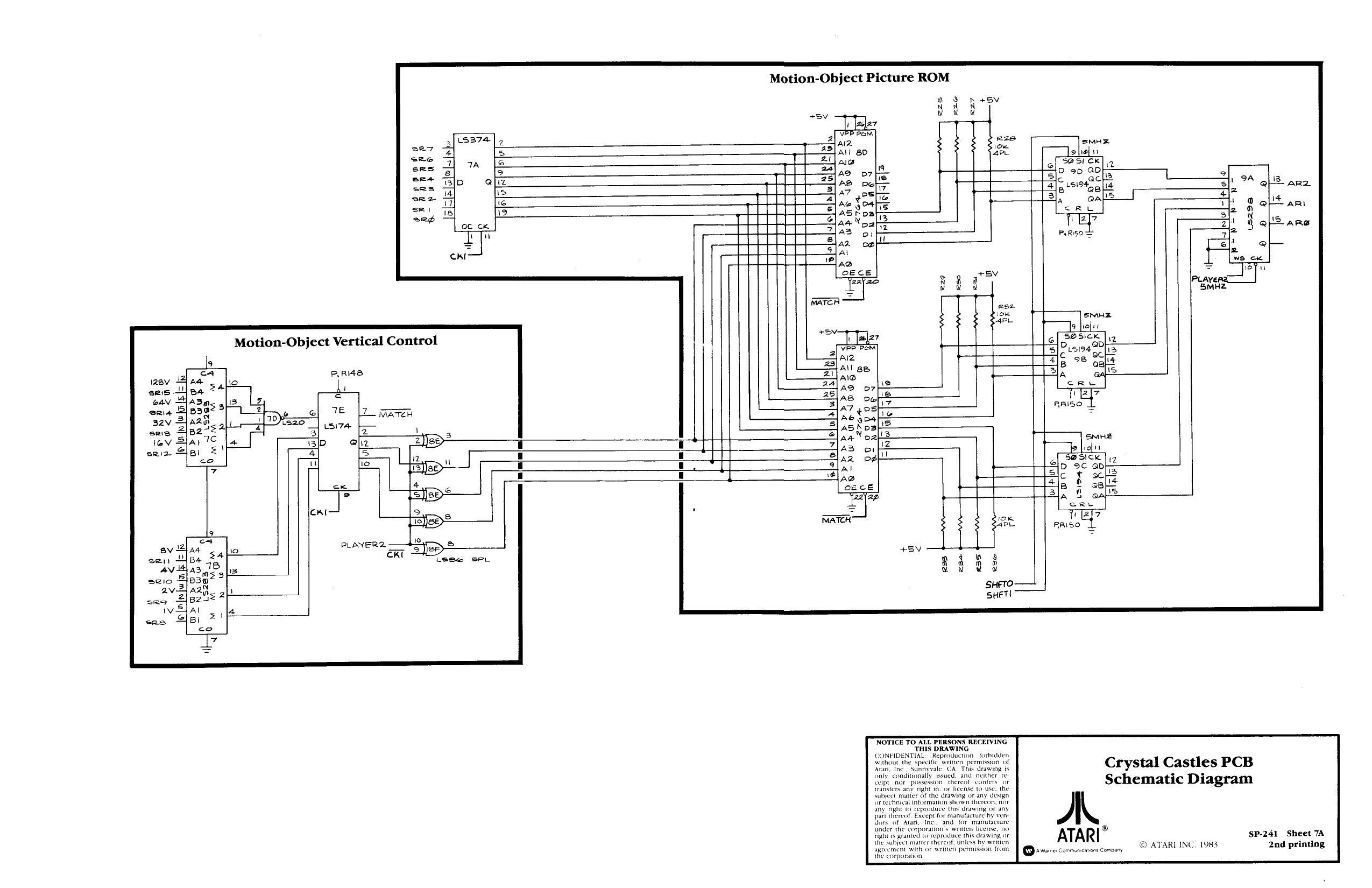
Motion-Object Vertical Control
R48
Motion-Object Picture ROM
fader VER BGM ese
| Ald | 1%. | SMH | |
| All 8D | APL | elie | |
| Ae | a | S@SI CK 12 | |
| 24)09 | 07 | D 90 aD | |
| 25 | 1 | slo | acl |
| AS | be) | S194, | |
| Bes | 7, | 4] | tee [4 |
| a | ges | EIN | ale |
2/42 goths R ASRpa et
| Sl aa | obe | T 2]? |
pal Ey z 1%
| eS Az | o1 mI | PAROS |
Aa ce Al AD CECE +5V aay a> fe ¢ PLay. y
PLAYER2
| 27 | of | 225K] 2 |
vee Ten J 5] Presa fs Al2 7 Feo oe She
| All ae. | 38 | oats |
| ae | he | +4 |
| a2 | ore | TEP |
| ee | ie 17 | RRISO |
| t | Lo | = |
Pte)" S@SICK] 17
Ey
NOTICE TO ALL PERSONS RECEIVING THIS DRAWING CONFIDENTIAL: Reproduction forbidden. without the specific written permission of Atari, Ine. Sunnyvale, CA” This. dra only conditionally issued, Ceipt “nor possession. thereof confers or transfers any right in, or license to use, the subject matter of the drawing or any design Or technical information shown thereon, nor any fight to reproduce this drawing or any part thereof, Except for unufacture by ven: Mors of Atari, Inc,, and for manufacture under the corporation's weitten license, no.
fight is geanted to reproduce this deawing or
the subject matter thereof, unless by weitten agreement with oF written permission from, the corporation ola sf [-Jefo fo
Crystal Castles PCB
Schematic Diagram
A
ATARI”
2 w2106: commeorearions Comoany © ATARI INC. 1983 SP-241 Sheet 7A 2nd printing
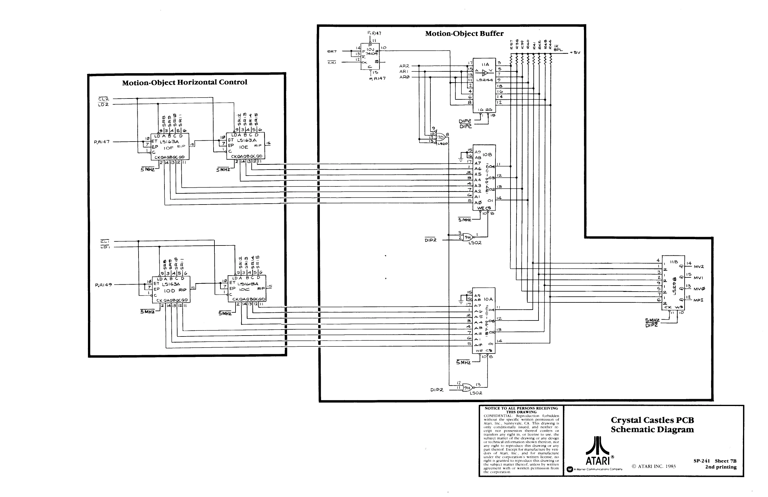
This page is a drawing, shown as the original scan.
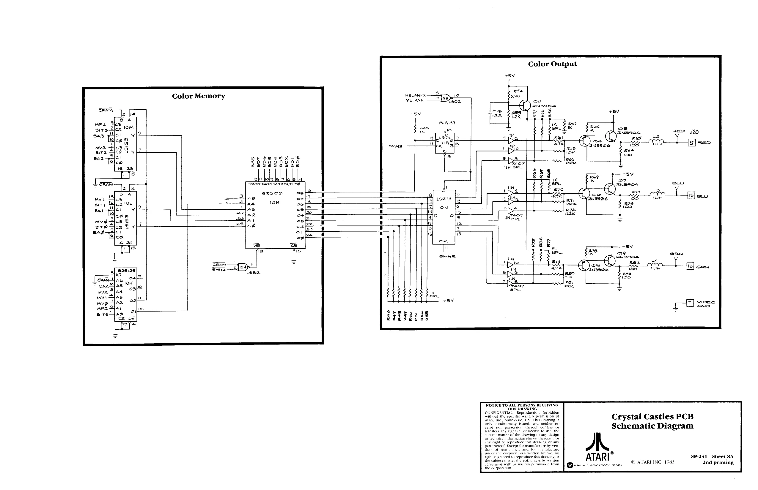
This page is a drawing, shown as the original scan.
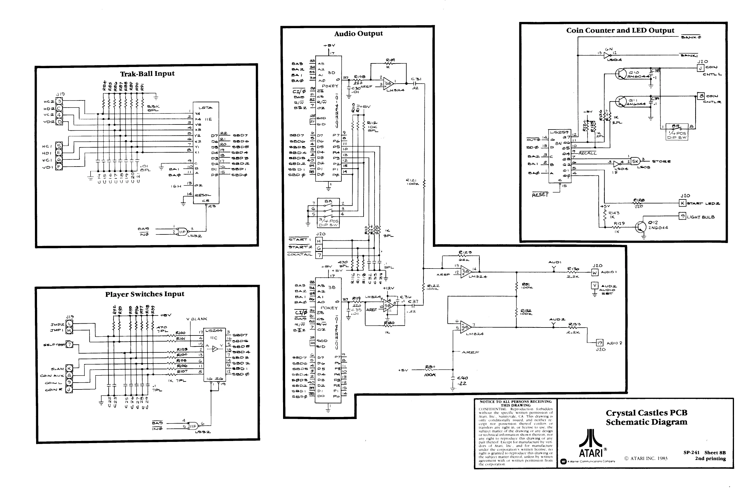
Trak-Ball Input
ha ~ PERERA
Player Switches Input
V BLANK
Audio Output
START. 3/4 Pos oF sw.
StART2
SSSA
BGRRQY corzz94-c1
v a2
Coin Counter and LED Output
Banks
J20 [iJeranr veo.
LIGHT BULB oz 2NGO44
NOTICE TO ALL PERSONS RECEIVING THIS DRAWING SONPIDENTIAL Reproduction forbidden without the specific written permission of Atari, Ine. sunnyvale, CA. This drawing is only conditionally issued. and neither ce: Celpt_ nor possession thereof conters or transfers any fight in, of license w use, the Subject matter Of the drawing or any design Of wWehnieal information shown thereon, nor any right to feproduce this drawing or any part thereof Except for manufacture by ven. Uors of Atari, Inc. and for manufacture Under the corporation's written license, no fight 1s granted to reproduce this drawing or the subject matter thereof, unless by written agecement With or weitten permission from. the corporation
Crystal Castles PCB
Schematic Diagram
A. ATARI . SP-241 Sheet 8B Qs reresconmncatonsconoany © ATARI INC. 1985 2nd printing
This page is a drawing, shown as the original scan.
This page is a drawing, shown as the original scan.
Crystal Castles Troubleshooting Guide
Crystal Castles”
Troubleshooting with the CAT Box
Troubleshooting with the Read/Write Controller
A. CAT Box Preliminary Set-Up
- Remove the electrical power from the game and the CAT Box. Remove the wiring harness from the game PCB. Remove the game PCB from the game cabinet. Remove Microprocessor 2C from the game PCB. Connect the harness from the game to the game PCB. Connect together the 60 and ©2 test points on the game PCB with the shortest possible jumper.
- Connect the WDDIS test point to ground.
- Connect the CAT Box flex cable to the game PCB edge test connector.
- Apply power to the game and to the CAT Box.
- Set CAT Box switches as indicated: a. TESTER SELF-TEST: OFF b. TESTER MODE: R/W ll. Press TESTER RESET.
- Connect the DATA PROBE to the CAT Box. Connect the DATA PROBE ground clip toa game PCB ground test point.
B. Checking the Address Lines
- Perform the CAT Box preliminary set-up.
- Set CAT Box switches as indicated:
a. BYTES: 1 b. PULSE MODE: UNLATCHED c. RAW MODE: (OFF) d. RAW: READ
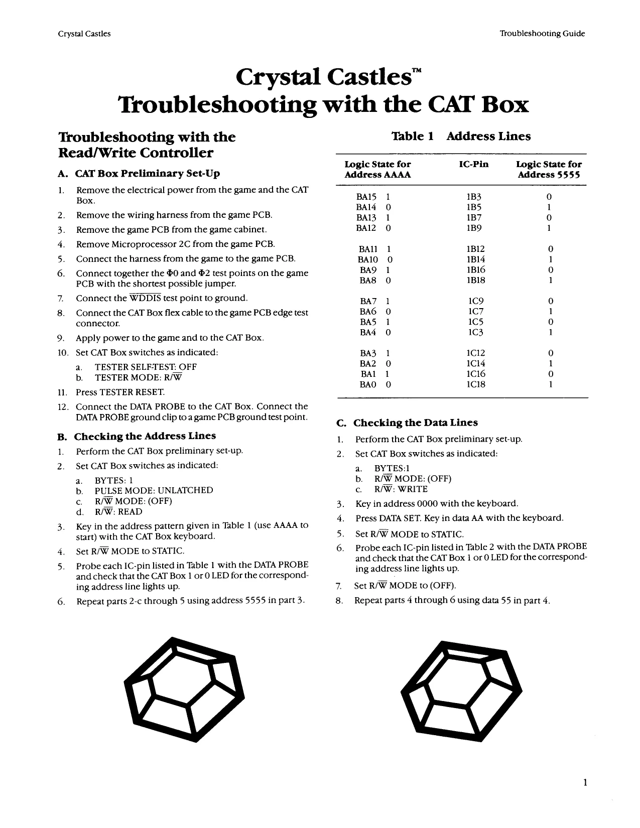
- Key in the address pattern given in Table 1 (use AAAA to start) with the CAT Box keyboard. 4, Set RAW MODE to STATIC. Probe each IC-pin listed in Table 1 with the DATA PROBE and check that the CAT Box 1 or 0 LED for the corresponding address line lights up.
- Repeat parts 2-c through 5 using address 5555 in part 3. a or Table 1 Address Lines
Logic State for IC-Pin Logic State for
Address AAAA Address 5555
| BAIS | 1 | 1B3 | 0 |
| BAl4 | 0 | 1B5 | 1 |
| BAIZ, | 1 | 1B7 | 0 |
| BAl2 | 0 | 1B9 | 1 |
| BA] | 1 | 1B12 | 0 |
| BAIO | 0 | 1B14 | 1 |
| BAO | 1 | 1B16 | 0 |
| BAS | 0 | 1B18 | 1 |
| BA7 | 1 | 1c9 | 0 |
| BAG | 0 | 1C7 | 1 |
| BAS | 1 | 1C5 | 0 |
| BA4 | 0 | 13 | 1 |
| BAZ | 1 | 1C12 | 0 |
| BA2 | 0 | 1C14 | 1 |
| BAL | 1 | 1C16 | 0 |
| BAO | 0 | 1C18 | 1 |
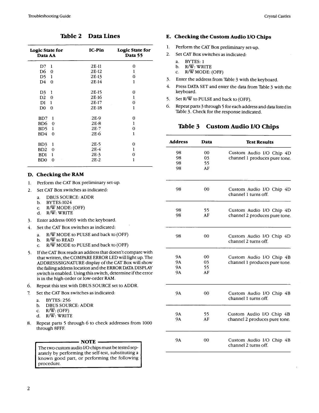
C. Checking the Data Lines Perform the CAT Box preliminary set-up.
- Set CAT Box switches as indicated:
a. BYTES:1 b. _ R/W MODE: (OFF) c. RAW: WRITE Key in address 0000 with the keyboard. Press DATA SET. Key in data AA with the keyboard. Set R/W MODE to STATIC. Probe each IC-pin listed in Table 2 with the DATA PROBE and check that the CAT Box 1 or 0 LED for the corresponding address line lights up. Set R/W MODE to (OFF).
- Repeat parts 4 through 6 using data 55 in part 4. ayae
~
Troubleshooting Guide
Table 2 Data Lines
Logic State for IC-Pin Logic State for Data AA Data 55
| D7 | 1 | 2E-11 | 0 |
| D6 | 0 | 2E-12 | 1 |
| DS | 1 | 2E-13 | 0 |
| D4 | 0 | 2E-14 | 1 |
| D3 | 1 | 2E-15 | 0 |
| D2 | 0 | 2E-16 | 1 |
| DI | 2E-17 | 0 | |
| DO | 0 | 2E-18 | 1 |
| BD7 | 1 | 2E-9 | 0 |
| BD6 | 0 | 2E-8 | 1 |
| BDS | 1 | 2E-7 | 0 |
| BD4 | 0 | 2E-6 | 1 |
| BD3 | 1 | 2E-5 | 0 |
| BD2 | 0 | 2E-4 | 1 |
| BDI | 1 | 2E-3 | 0 |
| BDO | 0 | 2E-2 | 1 |
D. Checking the RAM Perform the CAT Box preliminary set-up. Set CAT Box switches as indicated:
a, DBUS SOURCE: ADDR b. BYTES:1024 c. RAW MODE: (OFF) d. RAV: WRITE Enter address 0003 with the keyboard. Set the CAT Box switches as indicated: a. _R/W MODE to PULSE and back to (OFF) b. RAW to READ c. _ R/W MODE to PULSE and back to (OFF) If the CAT Box reads an address that doesn’t compare with that written, the COMPARE ERROR LED will light up. The ADDRESS/SIGNATURE display of the CAT Box will show the failing address location and the ERROR DATA DISPLAY switch is enabled. Using this switch, determine if the error is in the high-order or low-order RAM. Repeat this test with DBUS SOURCE set to ADDR. Set the CAT Box switches as indicated: a. BYTES: 256 b. DBUS SOURCE: ADDR c. RAW: (OFF) d. R/W: WRITE
Repeat parts 5 through 6 to check addresses from 1000
through 8FFF.
. Checking the Custom Audio I/O Chips
Perform the CAT Box preliminary set-up. Set CAT Box switches as indicated: a, BYTES: 1 b. RAW: WRITE c. RAW MODE: (OFF)
- Enter the address from Table 3 with the keyboard.
- Press DATA SET and enter the data from Table 3 with the keyboard.
- Set R/W to PULSE and back to (OFF).
- Repeat parts 3 through 5 for each address and data listed in Table 3. Check for the response indicated.
Table 3. Custom Audio I/O Chips
Address Data Test Results
| 98 | 00 | Custom Audio I/O Chip 4D |
| 98 | 03 | channel 1 produces pure tone. |
98 55 98 AF
| 98 | 00 | Custom Audio I/O Chip 4D |
channel 1 turns off.
| 98 | 55 | Custom Audio I/O Chip 4D |
| 98 | AF | channel 2 produces pure tone. |
| 98 | 00 | Custom Audio I/O Chip 4D |
channel 2 turns off.
| 9A | 00. | Custom Audio I/O Chip 4B |
| 9A | 03 | channel 1 produces pure tone. |
9A 55 9A AF
| 9A | 00. | Custom Audio I/O Chip 4B |
channel 1 turns off.
| 9A | 55 | Custom Audio I/O Chip 4B |
| 9A | AF | channel 2 produces pure tone. |
| 9A | 00. | Custom Audio 1/O Chip 4B |
channel 2 turns off.
Crystal Castles
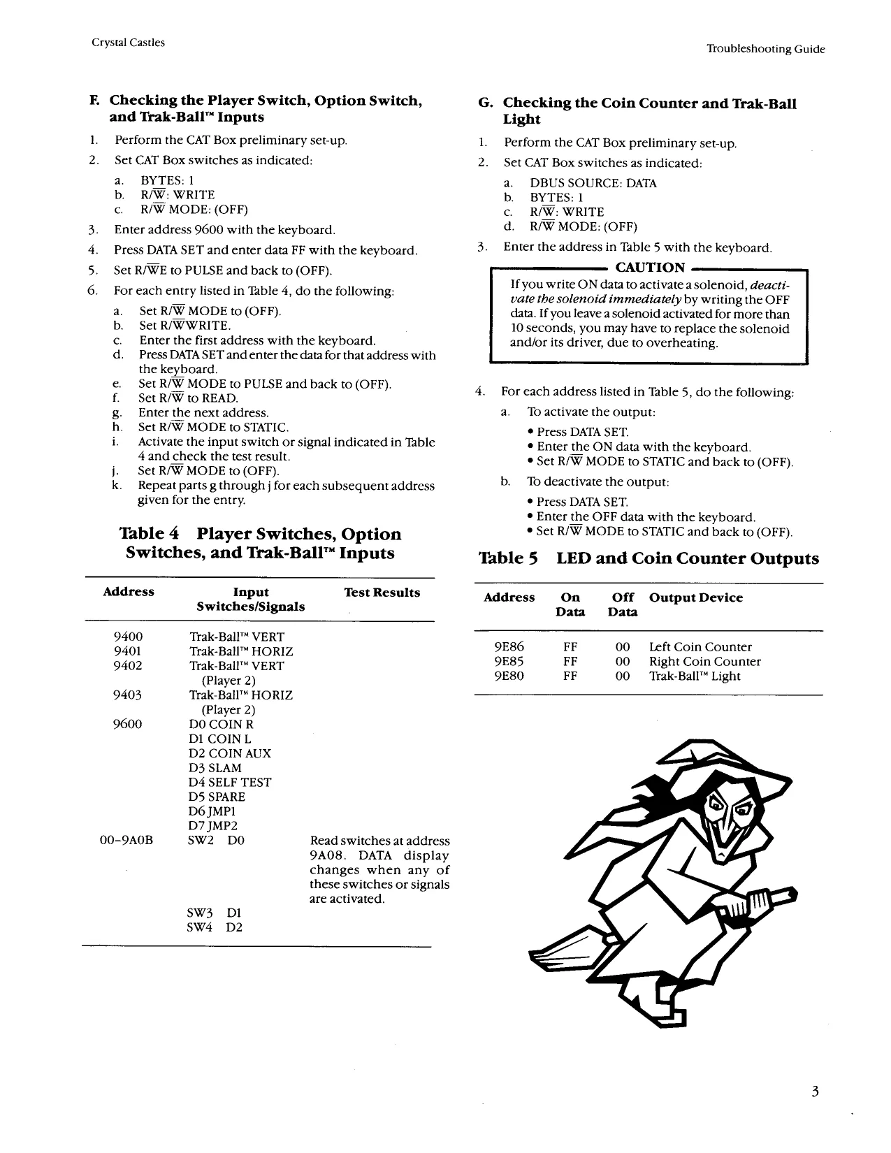
FE. Checking the Player Switch, Option Switch, and Trak-Ball™ Inputs
- Perform the CAT Box preliminary set-up.
- Set CAT Box switches as indicated: a. BYTES: 1 b. R/W: WRITE cc. RAW MODE: (OFF) Enter address 9600 with the keyboard. Press DATA SET and enter data FF with the keyboard. Set R/WE to PULSE and back to (OFF). For each entry listed in Table 4, do the following: Set R/W MODE to (OFF). Set R/WWRITE. Enter the first address with the keyboard. Press DATA SET and enter the data for that address with the keyboard. Set R/W MODE to PULSE and back to (OFF) Set R/W to READ. Enter the next address. Set R/W MODE to STATIC. Activate the input switch or signal indicated in Table 4and check the test result. Set R/W MODE to (OFF). k. Repeat parts g through j for each subsequent address given for the entry. aAwae
aoe
roe me
Table 4 Player Switches, Option
Switches, and Trak-Ball™ Inputs
Address Input Test Results
Switches/Signals
9400 Trak-Ball™ VERT 9401 Trak-Ball™ HORIZ 9402 Trak-Ball™ VERT (Player 2) 9403 Trak-Ball™ HORIZ (Player 2) 9600 DO COINR DI COINL D2 COIN AUX D3 SLAM D4 SELF TEST D5 SPARE D6 JMP1 D7 JMP2 00-9A0B sW2 DO
are activated. sw3 DI sw4 D2 Read switches at address 9A08. DATA display changes when any of these switches or signals Troubleshooting Guide
G. Checking the Coin Counter and Trak-Ball Light
- Perform the CAT Box preliminary set-up.
- Set CAT Box switches as indicated:
a, DBUS SOURCE: DATA b. BYTES: 1 c. RAW: WRITE d. RAW MODE: (OFF)
- Enter the address in Table 5 with the keyboard.
- For each address listed in Table 5, do the following: a. To activate the output: Press DATA SET. ¢ Enter the ON data with the keyboard. © Set R/W MODE to STATIC and back to (OFF). b. To deactivate the output:
Press DATA SET. Enter the OFF data with the keyboard. Set R/W MODE to STATIC and back to (OFF).
Table 5 LED and Coin Counter Outputs
Address On Off Output Device
Data Data
| 9E86 | FF | 00 | Left Coin Counter |
| 9E85 | FF | 00 | Right Coin Counter |
| 9E80 | FF | 00 | Trak-Ball™ Light |
Troubleshooting Guide
Troubleshooting the Watchdog
Circuit
‘The Watchdog circuit will send continuous reset pulses to the microprocessor ifa problem exists within the microprocessor circuit. If the self-test fails to run, it is a good practice to check the RESET line. RESET is a microprocessor input (pin 40). In a properly operating game, reset should occur during power-up or when the RESET test point is grounded. A pulsing RESET line indicates that something is causing the microprocessor to lose its place within the program. Typical causes are:
- Open or shorted address or data bus lines. Crystal Castles
- Bad microprocessor chip.
- Bad bus buffers.
- Bad ROM.
- Bad RAM. 6. Any bad input or output that causes an address or data line to be held in a constant high or low state. A pulsing RESET signal indicates a problem exists somewhere within the microprocessor circuitry. To aid in troubleshooting, the WDDIS test point can be connected toa ground test point to prevent resets. This will sometimes allow the Self-Test to be used to diagnose the failure during a RESET condition.