Paperboy SP-275 1st Printing
Paperboy (rev 3) (Atari Games, 1984) · Schematic Package · 33 pages · 72 sections · original scan
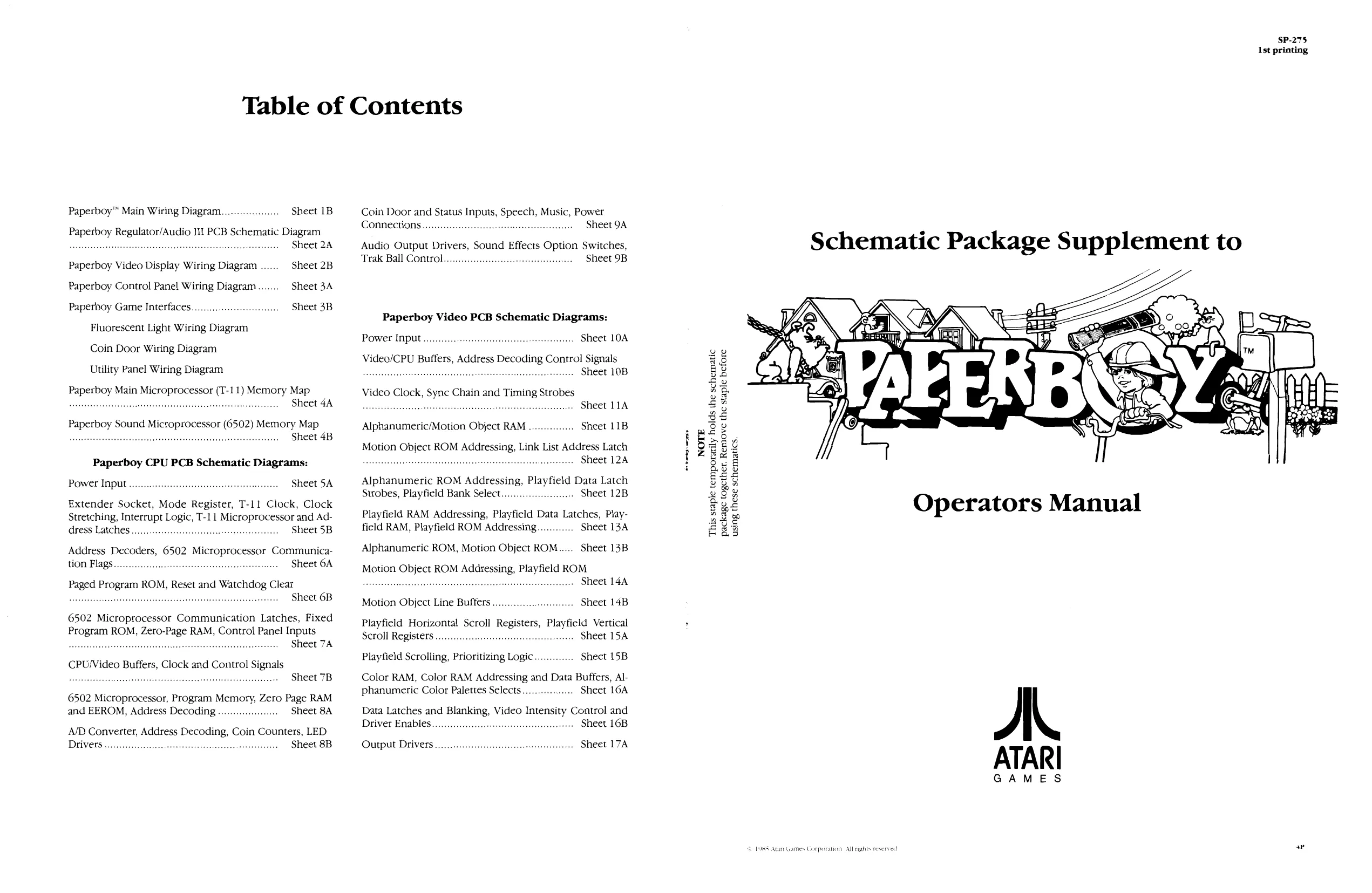
Table of Contents
Paperboy™ Main Wiring Diagram......... Sheet 1B
Paperboy Regulator/Audio Ii PCB Schematic Diagram Sheet 24
Paperboy Video Display Wiring Diagram Sheet 2B
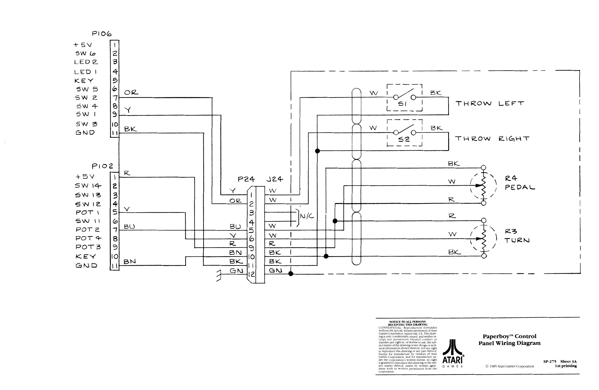
Paperboy Control Panel Wiring Diagram....... Sheet 3A
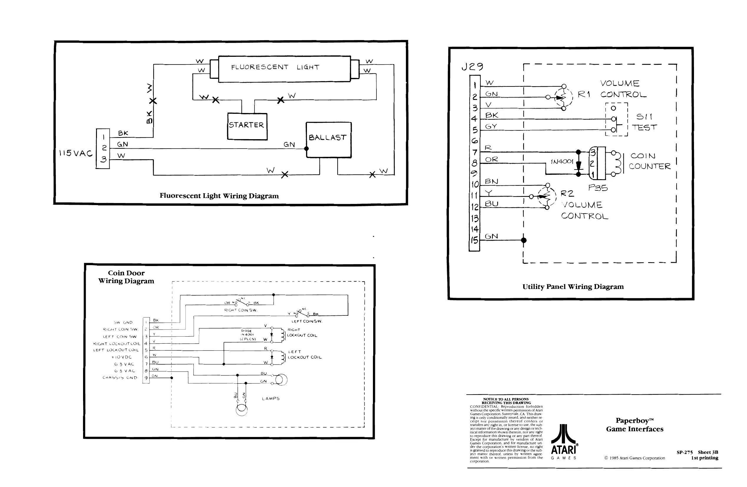
Paperboy Game Interfaces. Sheet 3B
Fluorescent Light Wiring Diagram
Coin Door Wiring Diagram
Utility Panel Wiring Diagram
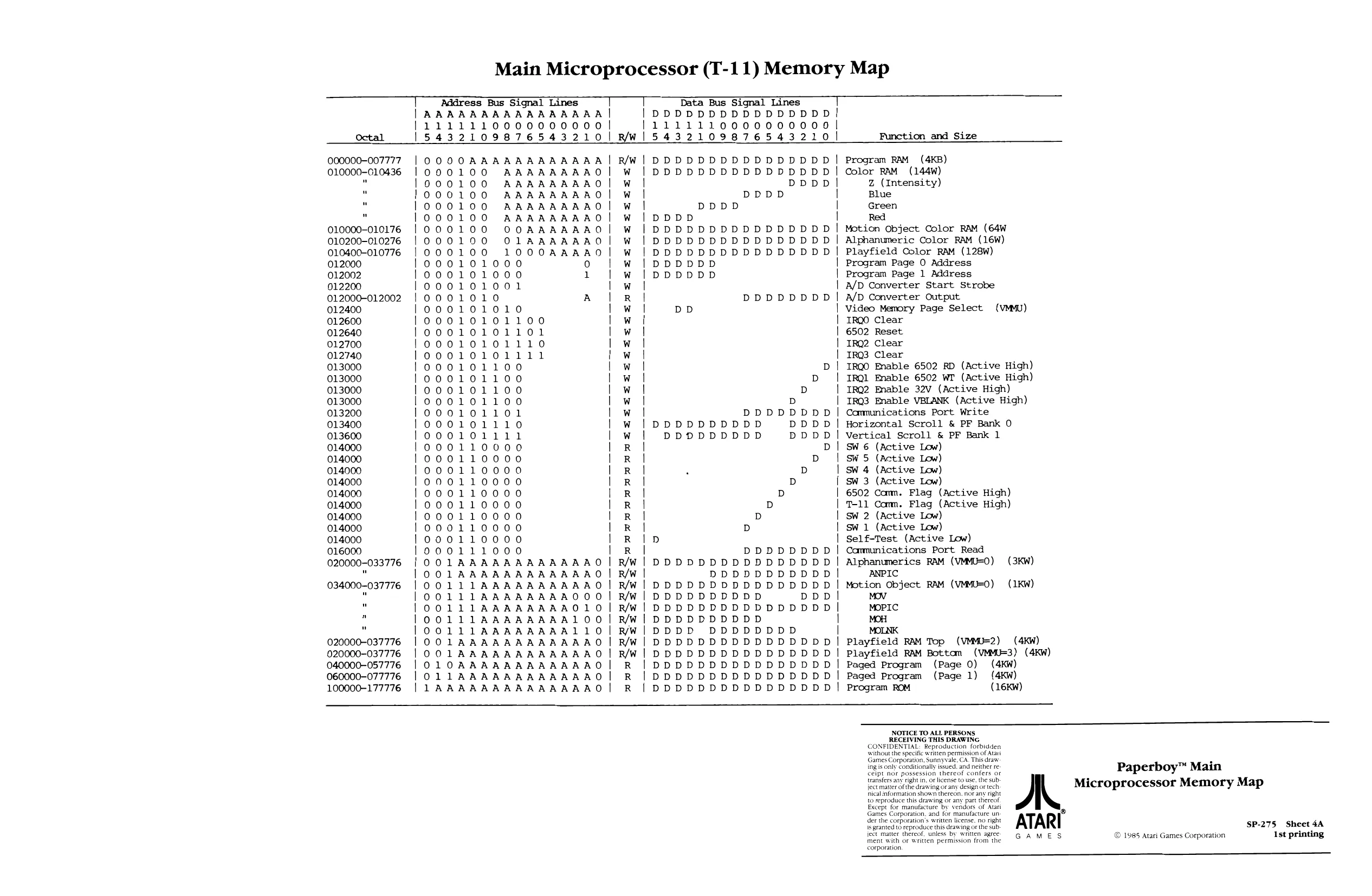
Paperboy Main Microprocessor (T-11) Memory Map agstsaceiseey caseapien 7 Sheet 4A
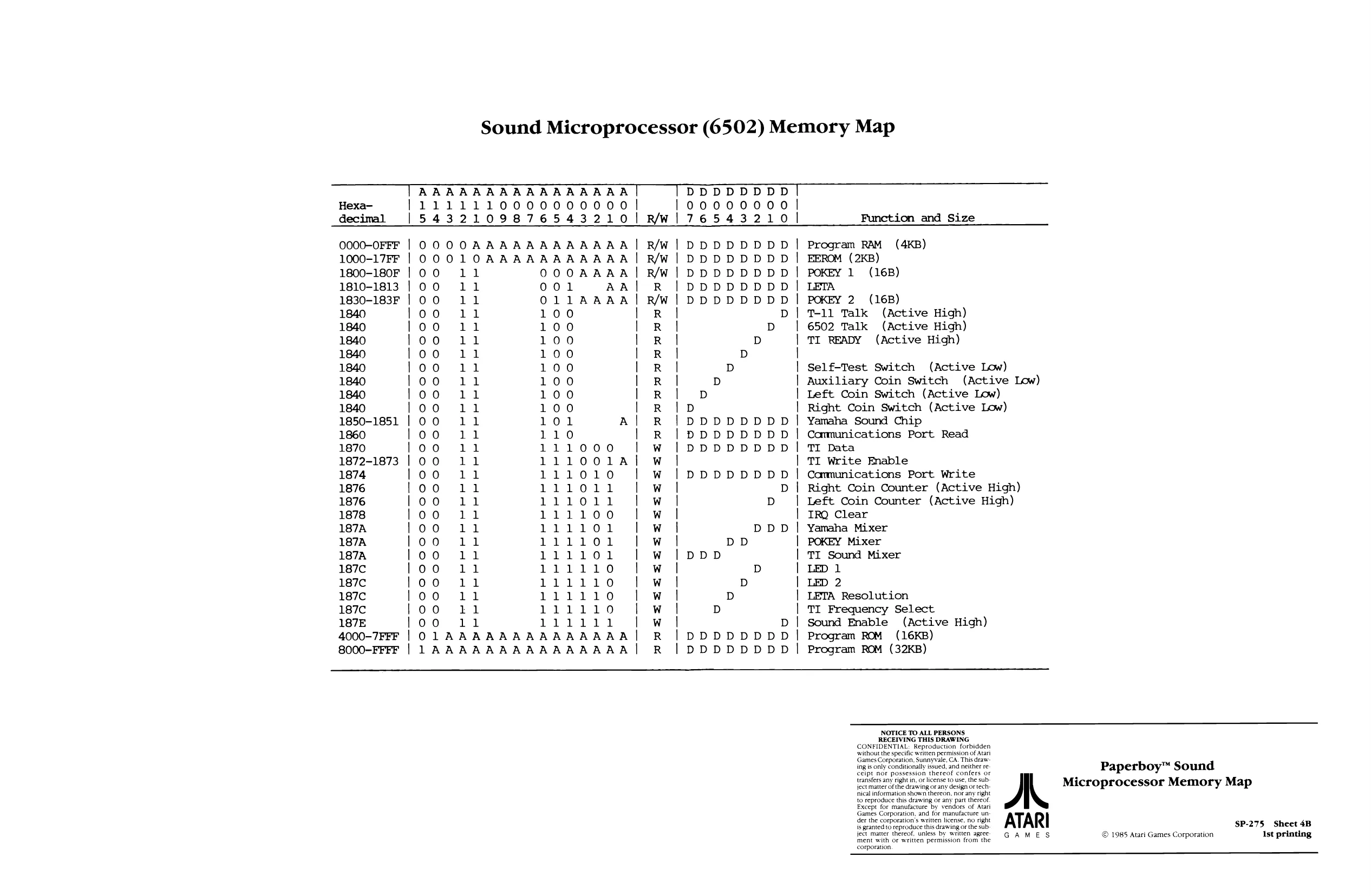
Paperboy Sound Microprocessor (6502) Memory Map
Paperboy CPU PCB Schematic Diagrams:
Power Input....... Sheet SA
Extender Socket, Mode Register, T-11 Clock, Clock Stretching, Interrupt Logic, T-11 Microprocessor and Ad- Press LAtChes seccsssoreresrseenrsrnsareeire Sheet 5B
Address Decoders, 6502 Microprocessor Communica- TOM FlagS oo. Sheet OA Paged Program ROM, Reset and Watchdog Clear sisi iis AEEE Ene Sheet 6B 6502 Microprocessor Communication Latches, Fixed Program ROM, Zero-Page RAM, Contro} Panel Inputs Sevstsnesssdssendetensorsreviesessingeesensnsesesse1s¥a Sheet 7A
Sheet 7B
6502 Microprocessor, Program Memory, Zero Page RAM and EEROM, Address Decoding ... Sheet 8A
A/D Converter, Address Decoding, Coin Counters, LED Drivers ... Sheet 8B Coin Door and Status Inputs, Speech, Music, Power COMMECHONS ..... sees tec et eesteetenees Sheet 9A
Audio Output Drivers, Sound Effects Option Switches, Trak Ball Control.......... see Sheet 9B
Paperboy Video PCB Schematic Diagrams:
Power Input... Sheet 10A
Video/CPU Buffers, Address Decoding Control Signals . Sheet 10B
Video Clock, Syne Chain and Timing Strobes in a . Sheet 11A
Alphanumeric/Motion Object RAM ............+. Sheet 11B
Motion Object ROM Addressing, Link List Address Latch cescseeteseeectetesesenereseeeseseeettiseneesstases . Sheet 124
Alphanumeric ROM Addressing, Playfield Data Latch Strobes, Playfield Bank Select..........0.000+ Sheet 12B
Playfield RAM Addressing, Playfield Data Latches, Playfield RAM, Playfield ROM Addressing............ Sheet 13A
Alphanumeric ROM, Motion Object ROM...... Sheet 13B
Motion Object ROM Addressing, Playfield ROM seeasaseageeusnigunstensenenesyss tgs es ogutyer sates . Sheet 14A Motion Object Line Buffers ...... : Sheet 14B
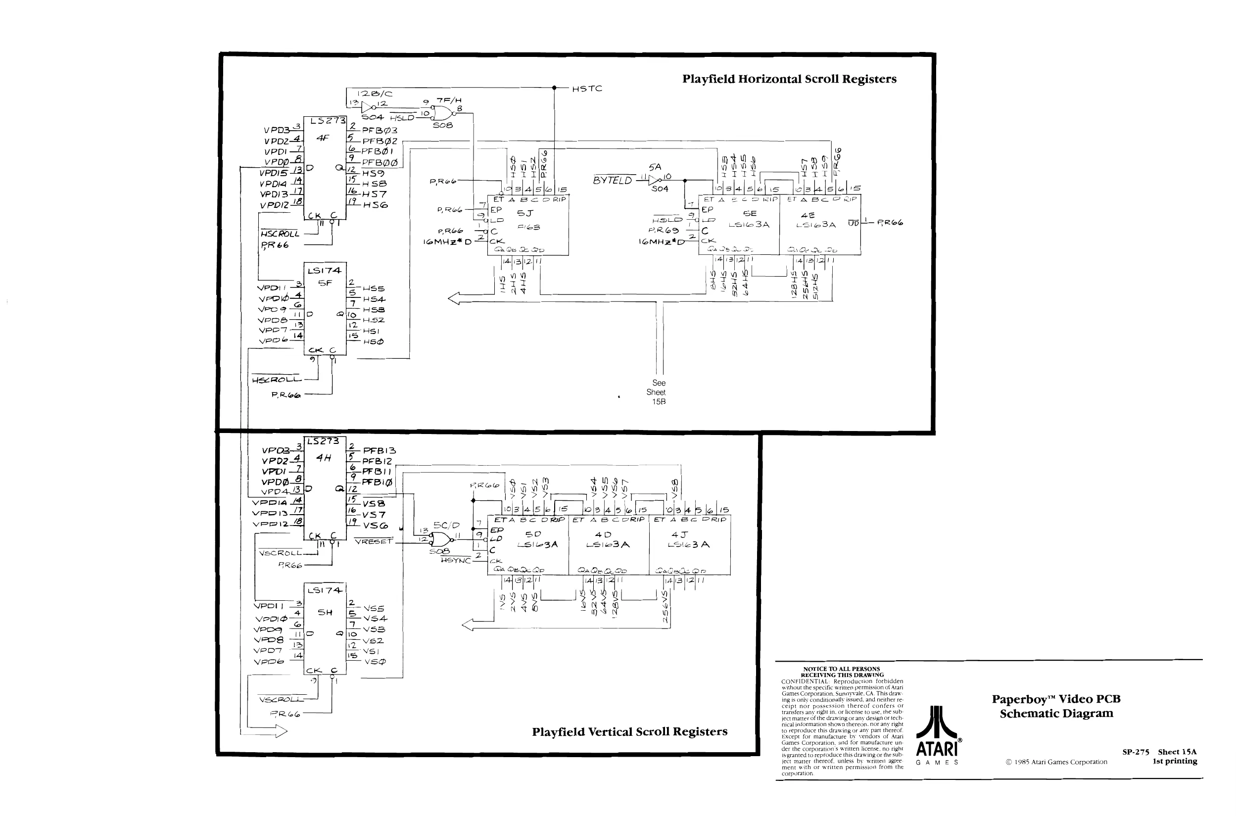
Playfield Horizontal Scroll Registers, Playfield Vertical Scroll Registers .......ceeeeee . Sheet 154
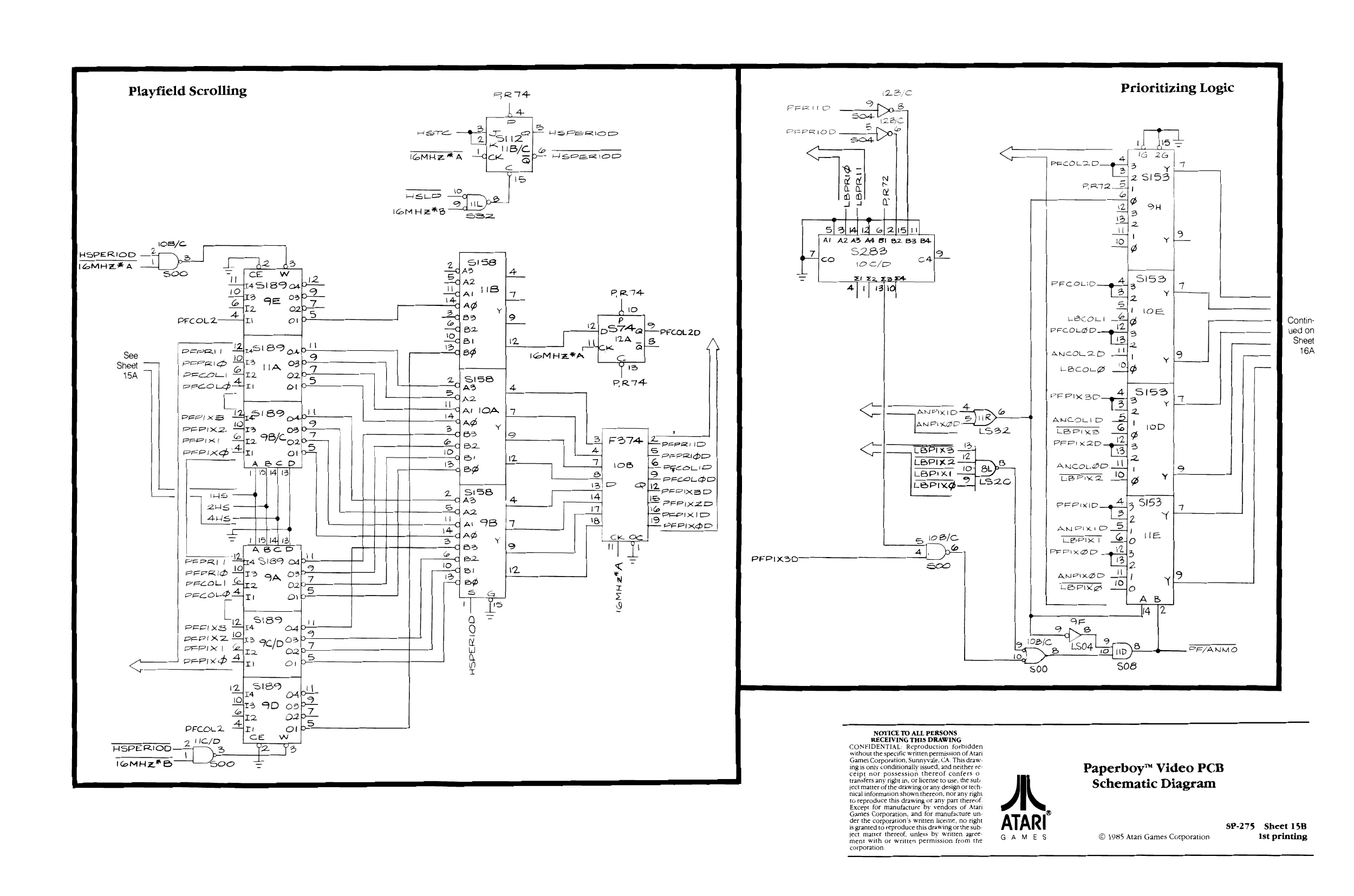
Sheet 15B
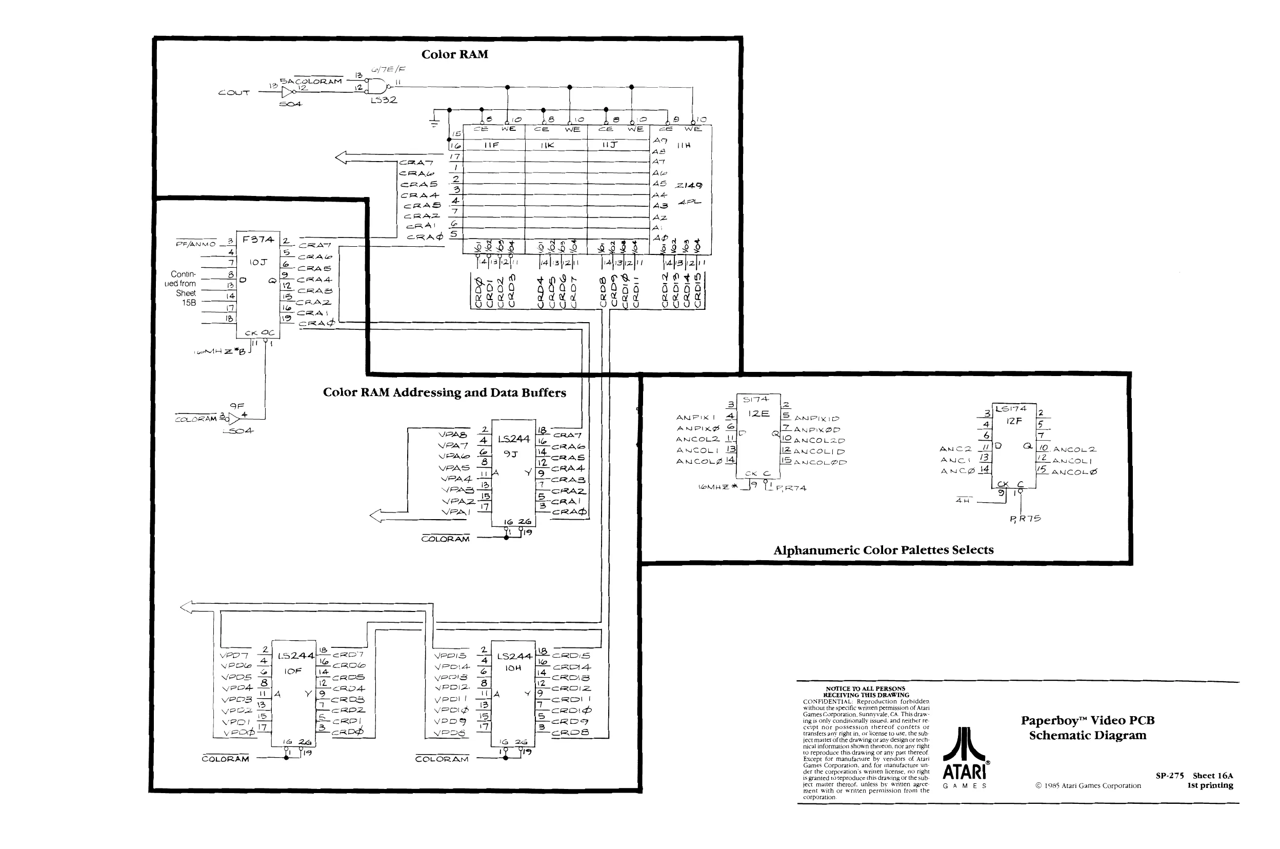
Color RAM, Color RAM Addressing and Data Buffers, Alphanumeric Color Palettes Selects............... Sheet 16A Playfield Scrolling, Prioritizing Logic.............
Data Latches and Blanking, Video Intensity Control and Driver Emables..........cccccceeseceee teen . Sheet 16B
Output Drivers......... Sheet 17A SP-275 1st printing
Schematic Package Supplement to
using these schematics. Operators Manual
A ATARI GAMES
LONS Anan Games Corporation All rights reserved aw
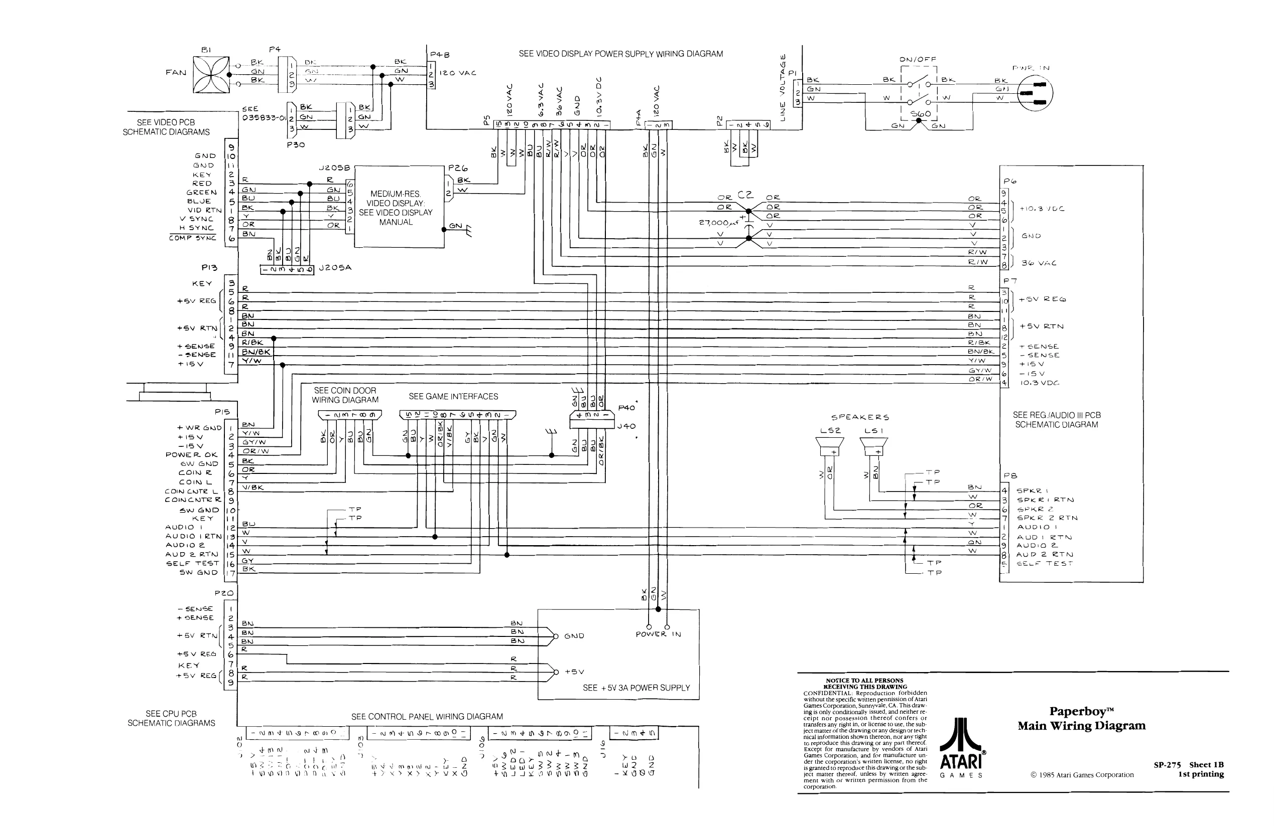
This page is a drawing, shown as the original scan.
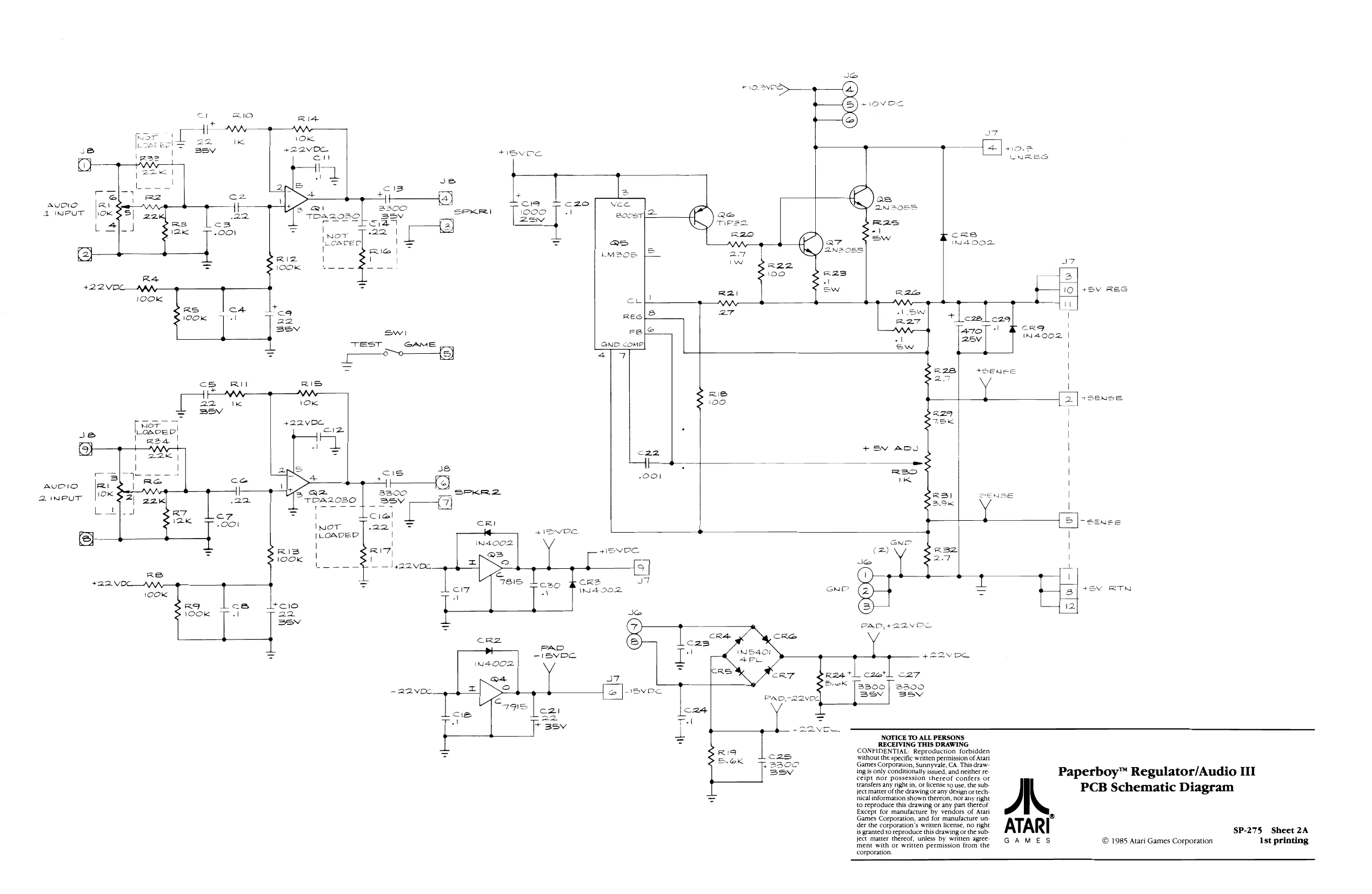
This page is a drawing, shown as the original scan.
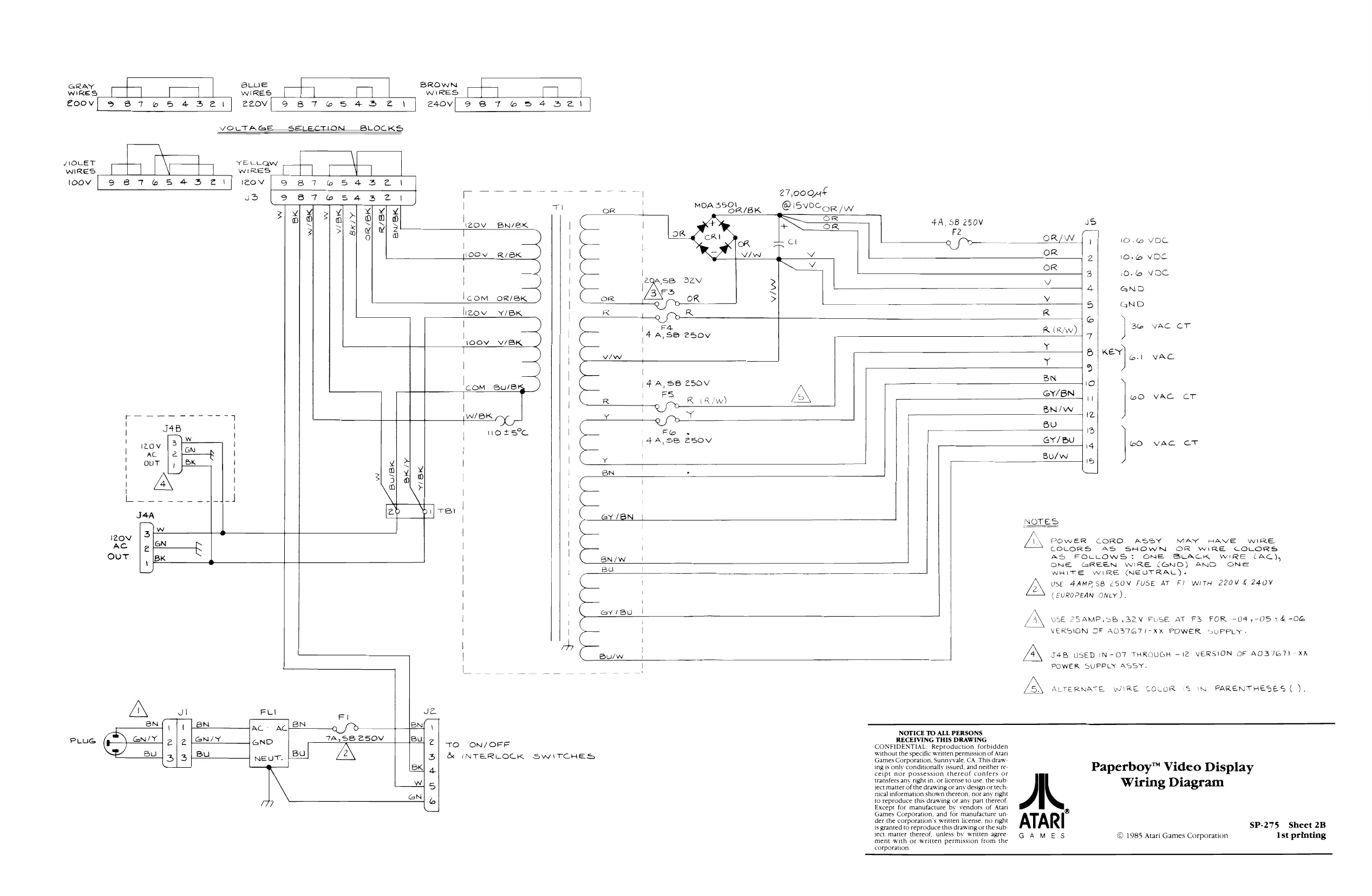
This page is a drawing, shown as the original scan.
This page is a drawing, shown as the original scan.
This page is a drawing, shown as the original scan.
This page is a drawing, shown as the original scan.
This page is a drawing, shown as the original scan.
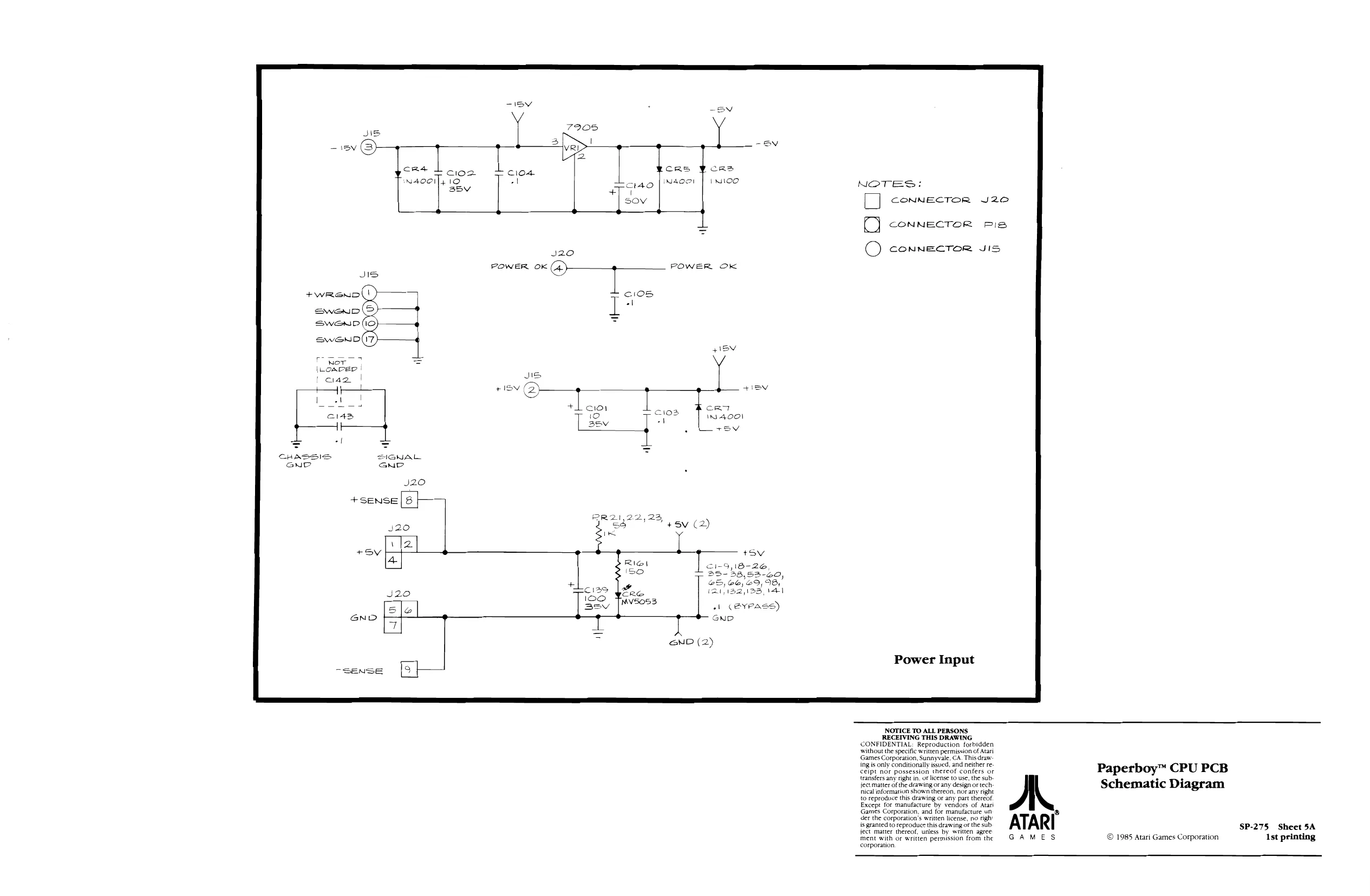
This page is a drawing, shown as the original scan.
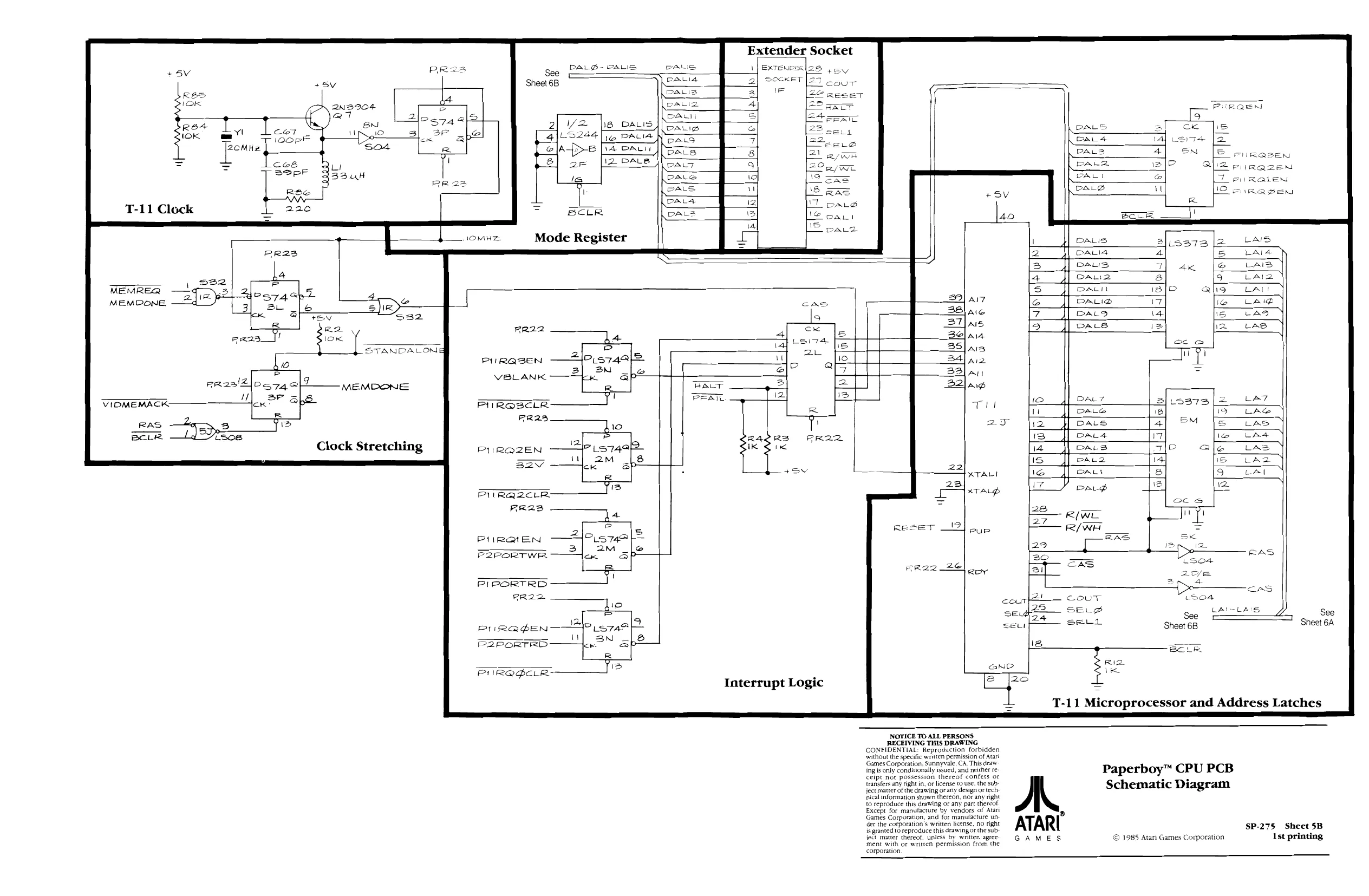
2NB904 Qt See Sheet 6B DAL®- CALI caus Extender Socket
Exre en
T-11 Clock BN. 2] Y2 |e Baus UPS 4{LS244 0 PAULA so4 o|a{>-6 fa Ac é
MEMREQ
MEMDONE,
STANDALONA
VIDMEMACK-
RAS :
BcLR LSOSs
Clock Stretching
I2 DALS CAA
Mode Register
BCLR
FR22
PHRQBEN
en ys PIIRQ2CLR:
FR23 As 2 2 PuiRateN —4°"s74e
P2PORTWR
PURQGEN
P2PORTRD
PrHR@PcLR~
Interrupt Logic
Fi R@LEN
FURASEN
NOTICE TO ALL PERSONS RECEIVING THIS DRAWING CONFIDENTIAL: Reproduction forbidden without the specific written permission of Atari Games Corporation, Sunnyvale, CA. This draw ing is only conditionally issued, and neither re: ceipt nox possession thereof confers or transfers any right in, or license (0 use, the subject matter of the drawing or any design or tech rica information shown thereon. nor any right to reproduce this drawing or any part thereof Except for manufacture by vendors of Atari Games Corporation, and for manufacture under the corporation's written license, no right is granted to reproduce this drawingor the sub ject mater thereof, unless by written. agree ment with of written permission from the corporation’ A
ATARI
GAMES
T-11 Microprocessor and Address Latches
vc
Paperboy™ CPU PCB Schematic Diagram
SP-275 Sheet 5B © 1985 Atari Games Cosporation Ist printing
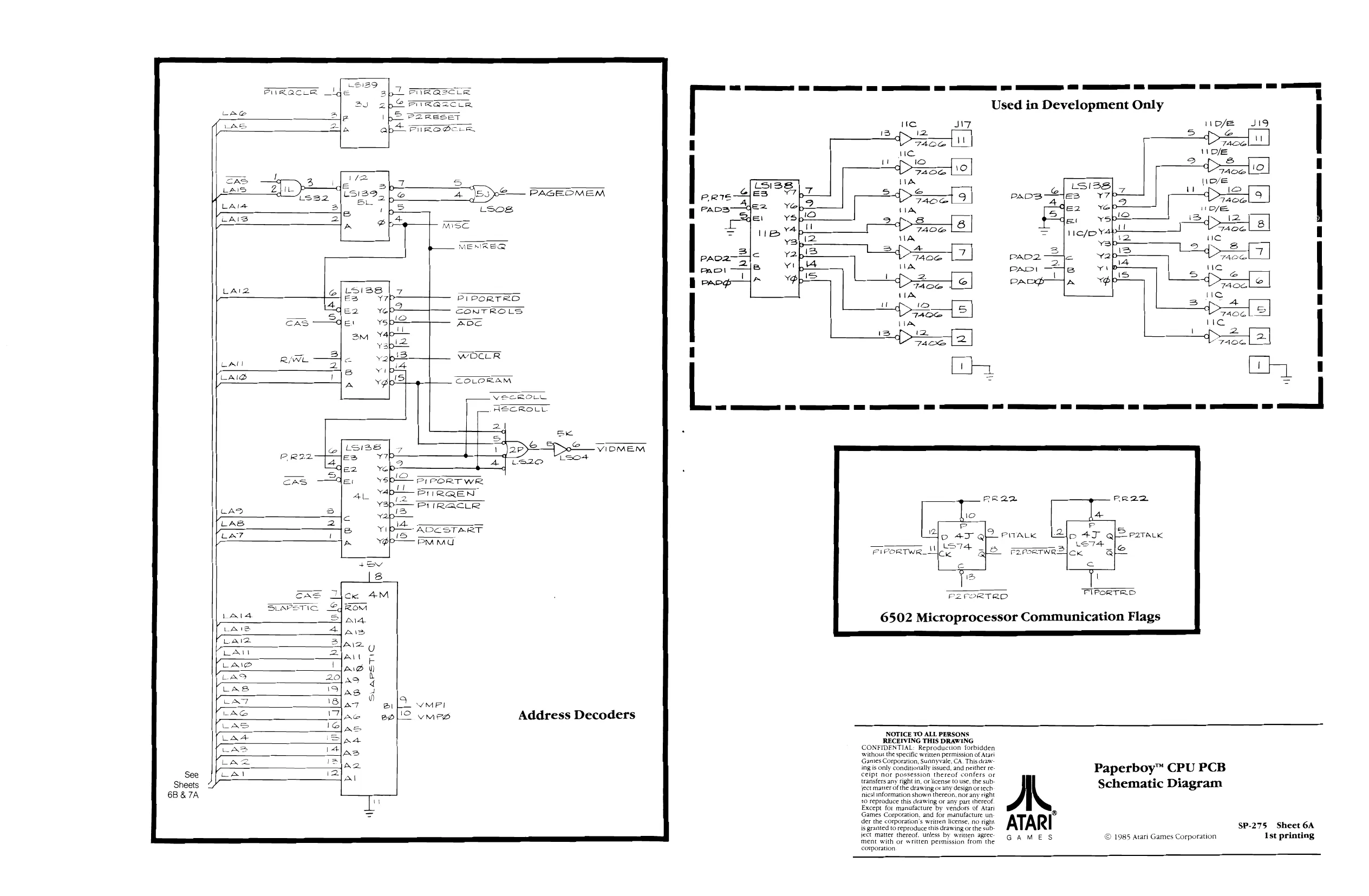
This page is a drawing, shown as the original scan.
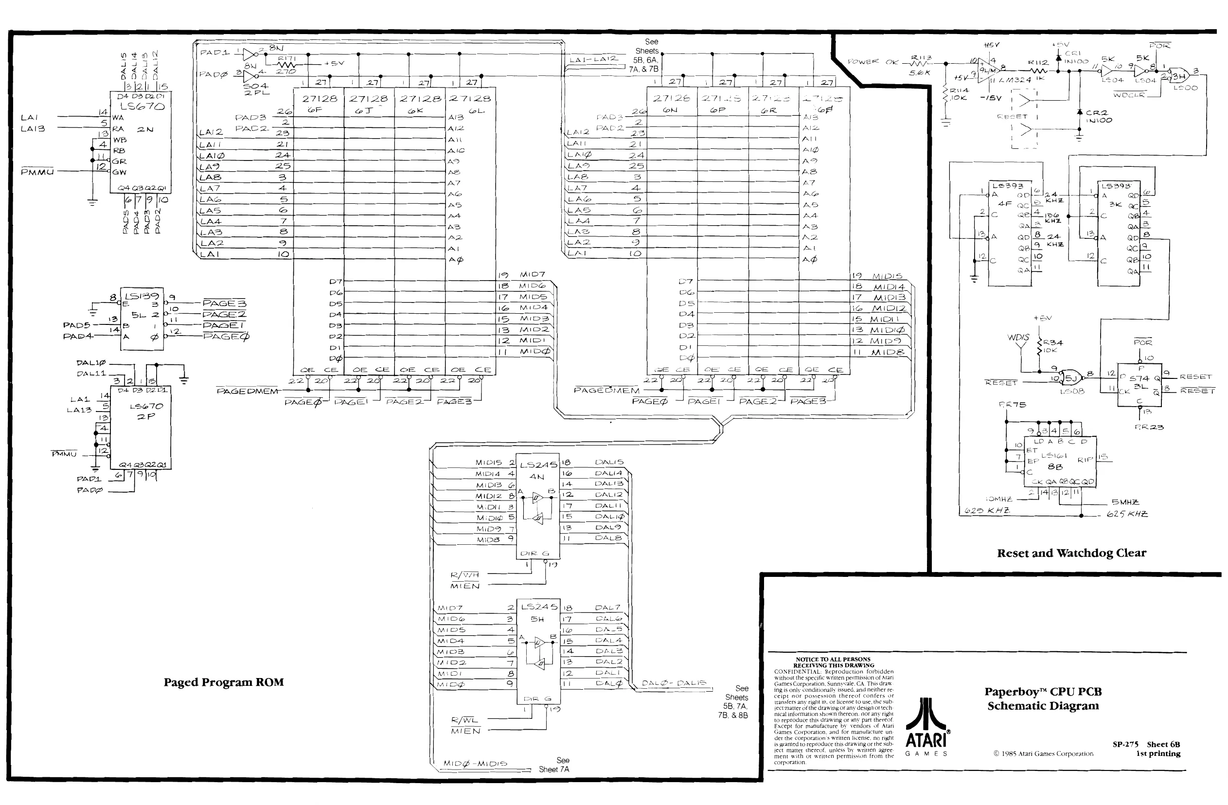
This page is a drawing, shown as the original scan.
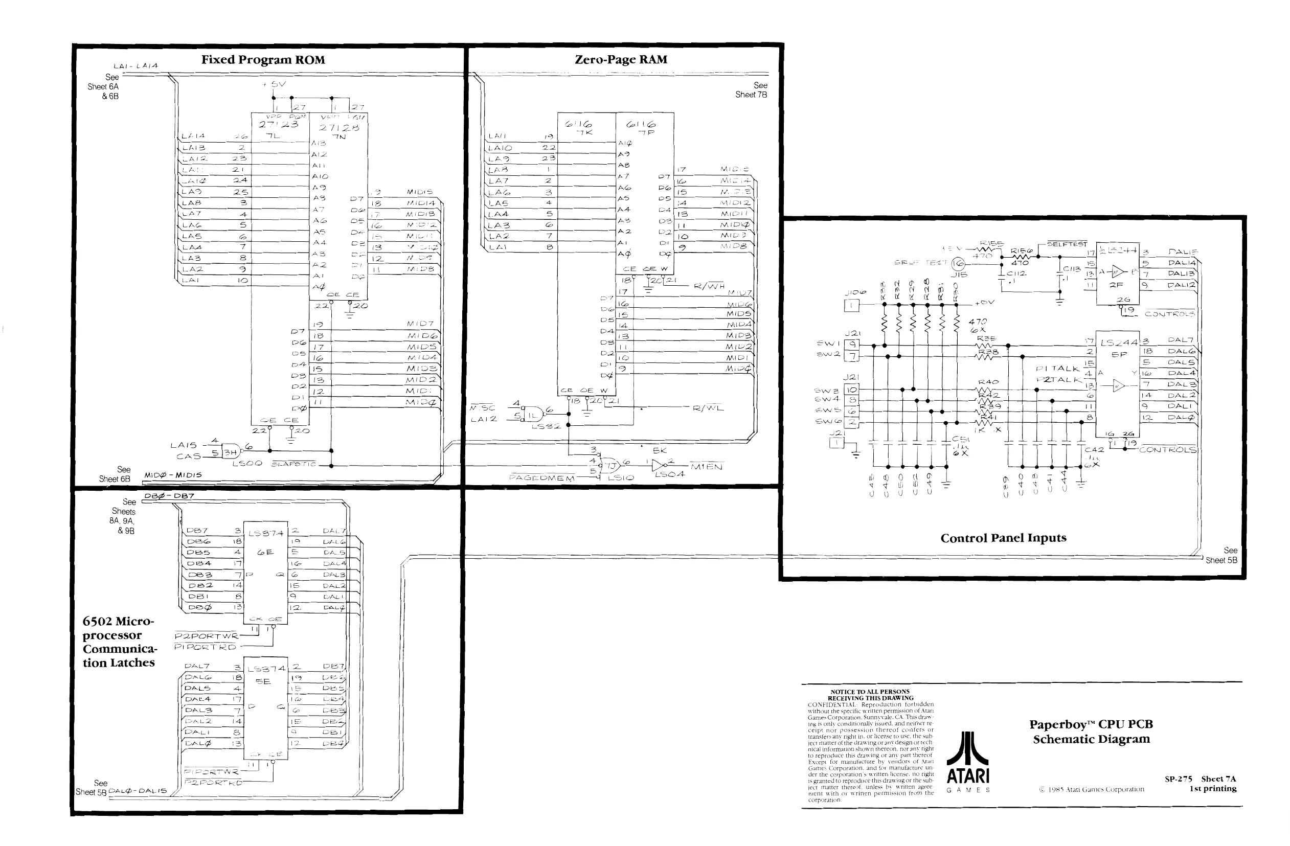
Fixed Program ROM
Zero-Page RAM
Sheet 6A &6B
See See Sheet 7B
Alp AD AS AT o7
AO be AS bs AA C4
Az c
LAIs +n
MiDg ~ MIDIS A
cas—2lay AL o BIN[Ofuys]o
- ag og
ce oe w ey oom wl = es A
liz
Sheet 6B
6502 Micro-
processor Communication Latches » DALY Control Panel Inputs
\ 16 =
| ces | 4 | GCE | a |
| oes | ay | le | DAL |
=) ee DAS
| ps2 | 4 | is | DALa| |
| os | 8 | Gi | CALL |
| cee | Zz | eacg| |
P2PORT WR:
PIPGRTRO
DALT
(ALG
CALS BALA ‘CALS ao fale
BAcI ae
NOTICE TO ALL PERSONS
RECEIVING THIS DRAWING
- Reproduction forbidden fic wnitten permission of Atar Games Corporation. Sunnyvale. CA. This draw ng is only conditionally issued. and neither re Ceipt nor pos thereof conters or teanslersany right in. of license (0 use. the sub ject matter of the drawing or any design or tech nical information shows thereon, nor any right to reproduce this drawing of anv part sbereot Except for manufacture by vendors of Ara Games Corporation, and fox Manufacture un der the corporation s writen license, NO right ss granted to reproduce this drawing or the sub: ject Matter thereof, unless by written agree With oF Wrinen permission from the Corporation| AL
ATARI
GAMES
Paperboy™ CPU PCB Schematic Diagram
SP-275 Sheet 7A Ist printing 1985 Atati Games Corpu
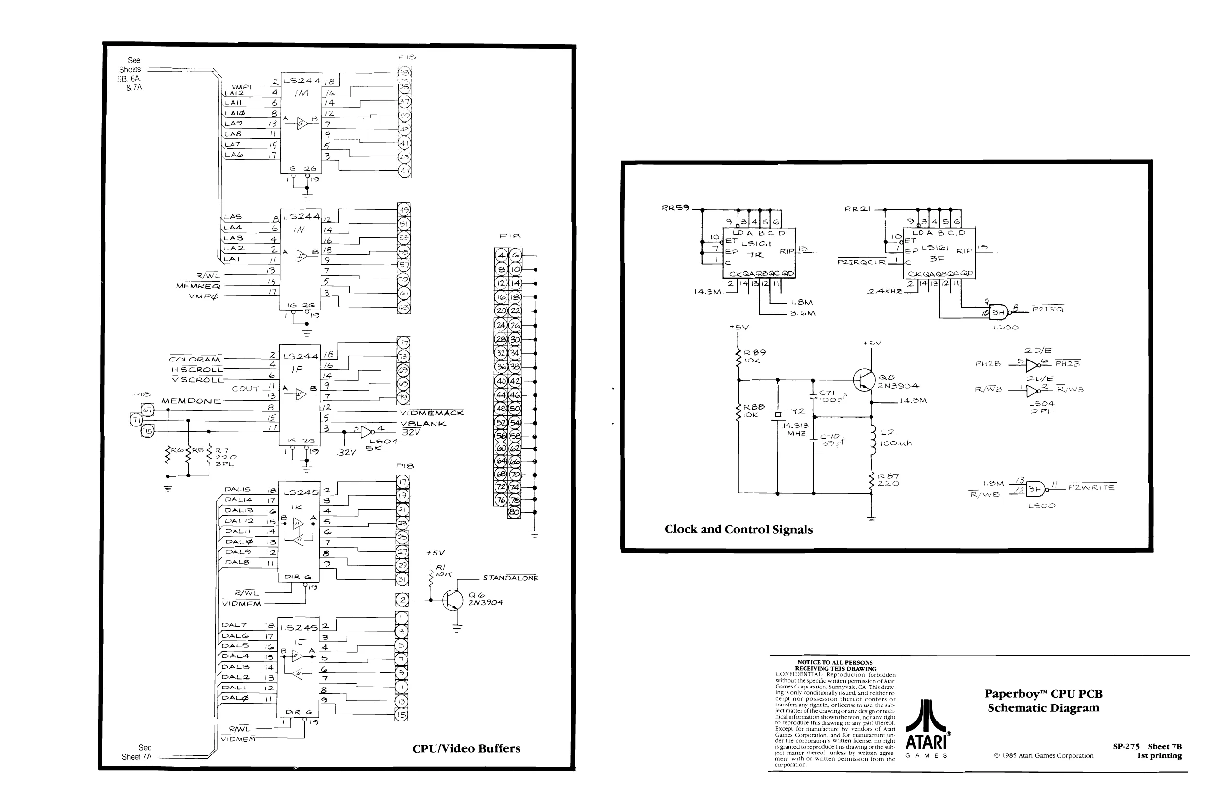
This page is a drawing, shown as the original scan.
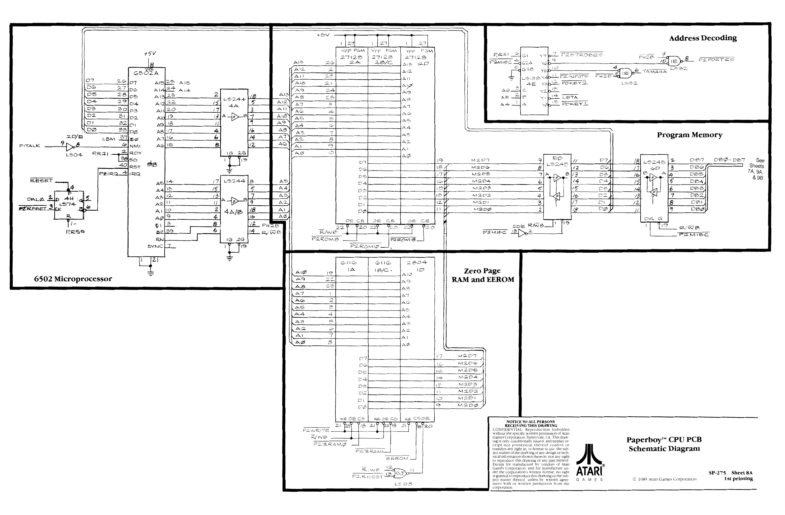
This page is a drawing, shown as the original scan.
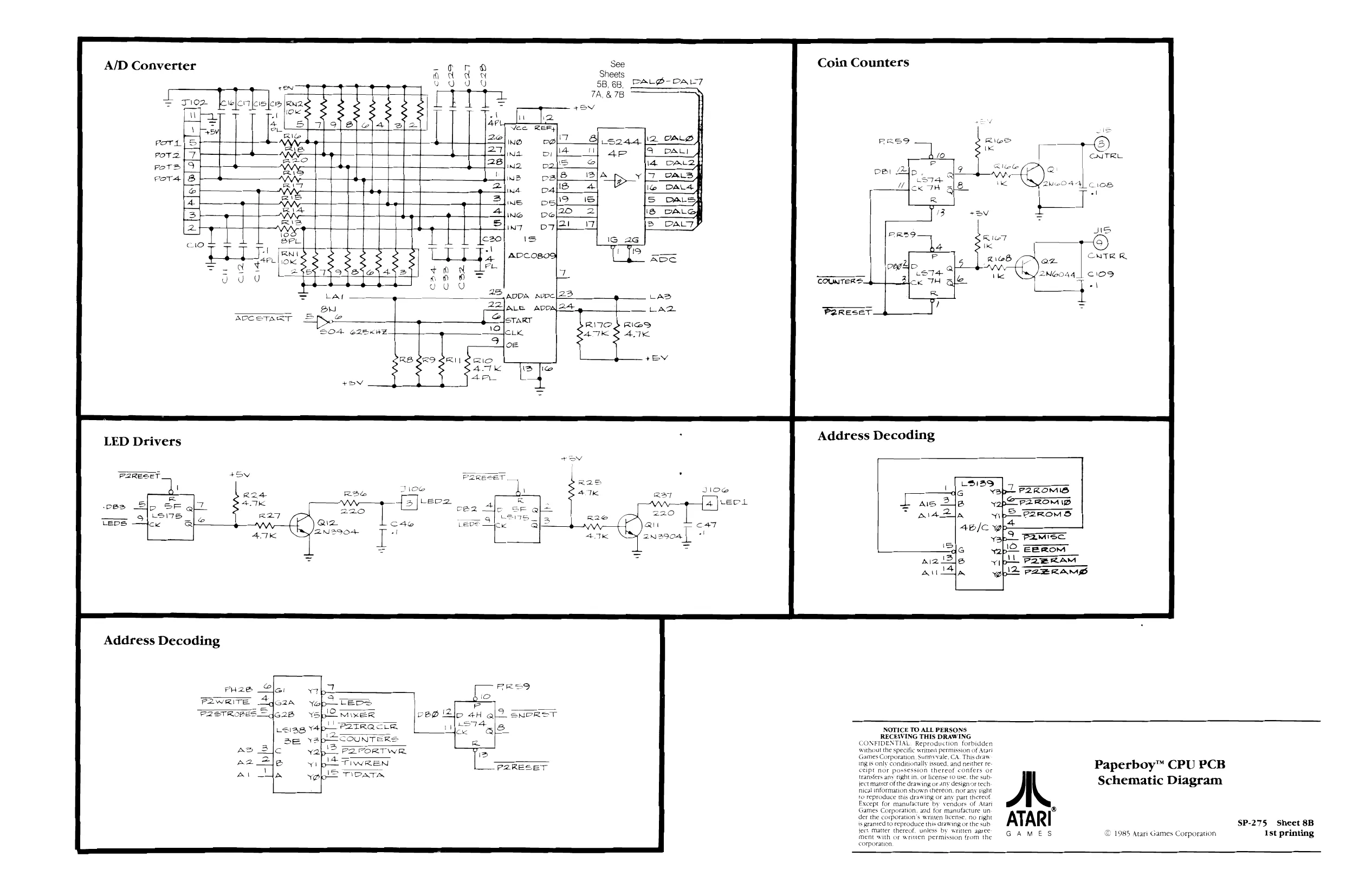
This page is a drawing, shown as the original scan.
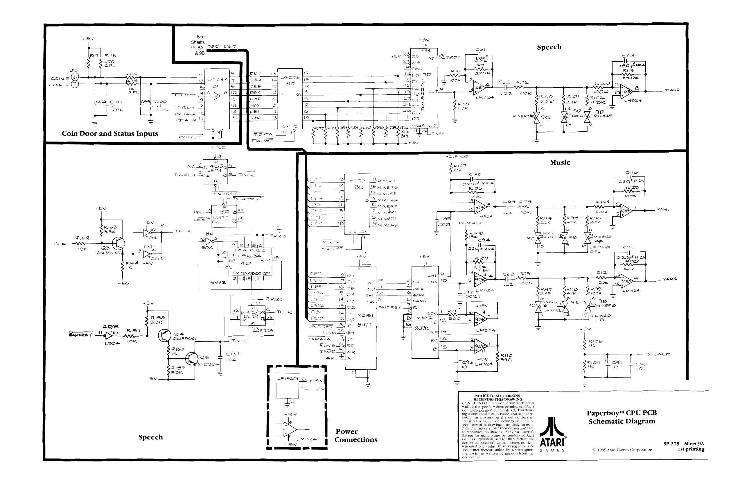
This page is a drawing, shown as the original scan.
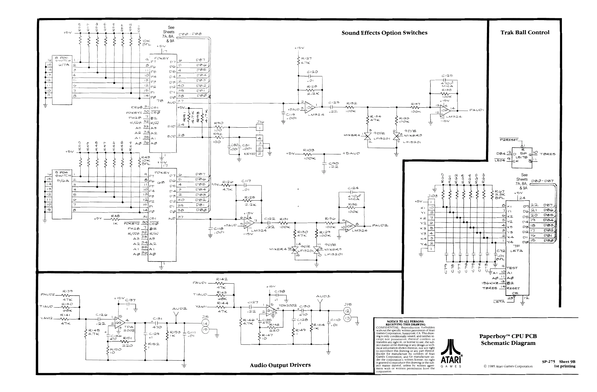
by
Pe pet
C4
PAUDZ,
Tiaup
yAM2 AUD2. Y TiAuo.
RIBS I... Ol gal
Sound Effects Option Switches
Rize
‘acle j 7 MiKBe A: LFIS201
- + 6 7 ooK look 10 Pep:
KIZ0 RI29 Maad
ATK 1oOK
Wo op/e
LL
es 1DA2002 ) a x fa 41°
q28 ear)
Audio Output Drivers
2 MIKER>
1D LEISZO! Lei2201 7 Lsiaao: Trak Ball Control
P2RESET. Ah Rg
9] usi7s TEDS Flee qu oe4 25 Se lO tenes
=A a9 AL aglaw
Lem
NOTICE TO ALL PERSONS RECEIVING THIS DRAWING CONFIDENTIAL: Reproduction forbidden ‘without the specific written permission of Atari ‘Games Corporation, Sunnyvale, CA. This draw ingis only conditionally issued, and neither ce ceipt nor possession thereof confers or transfers any right In, or license to use, the subject matter ofthe drawing or any design or tech nical inforination shown thereon, nor ay right to reproduce this drawing or any part thereof Except for manufacture by vendors of Atari Games Corporation, and for manufacture un: der the corporation's written license, no right is granted to reproduce this drawing or the sub. ject matter thereof. unless by wrnten agree: ment with of written permission from the corporation, A.
ATART
GAMES
Paperboy™ CPU PCB Schematic Diagram
SP-275 Sheet 9B © 1985 Atari Games Corporation Ist printing
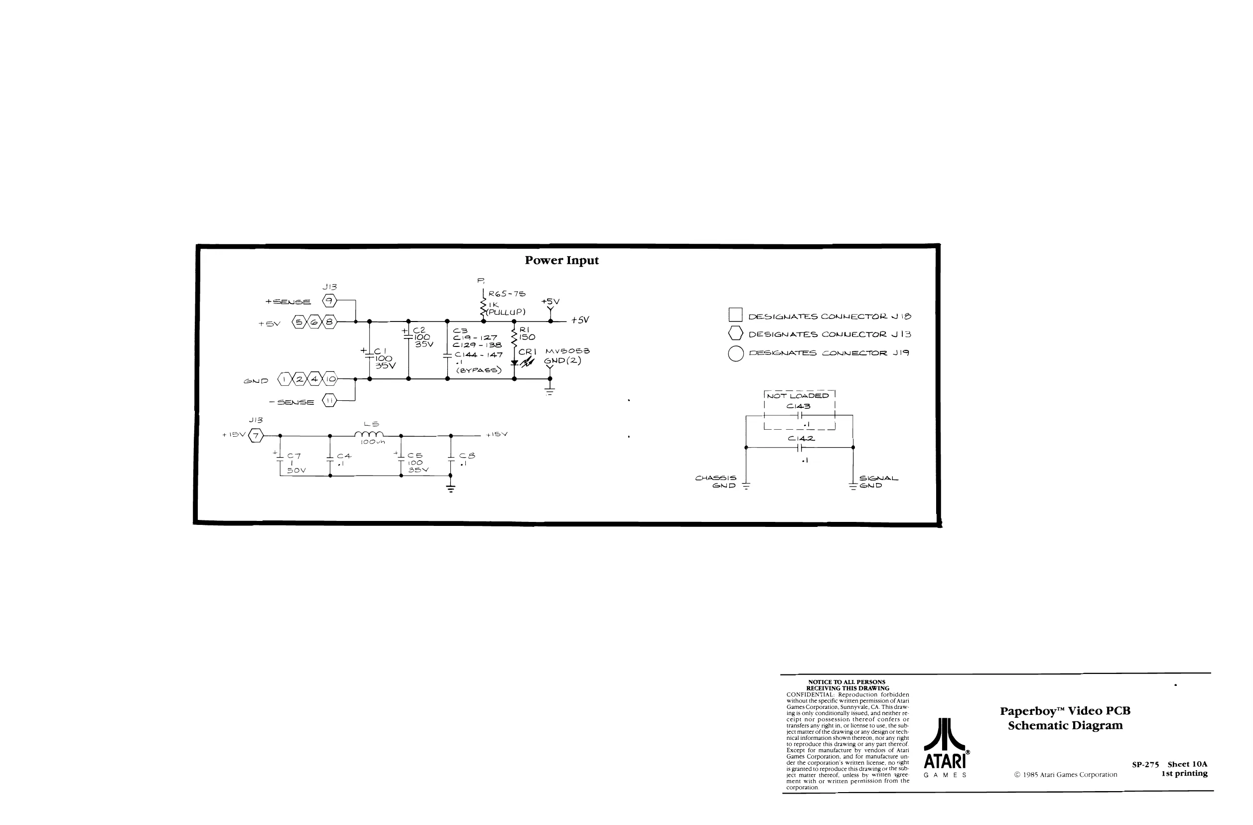
This page is a drawing, shown as the original scan.
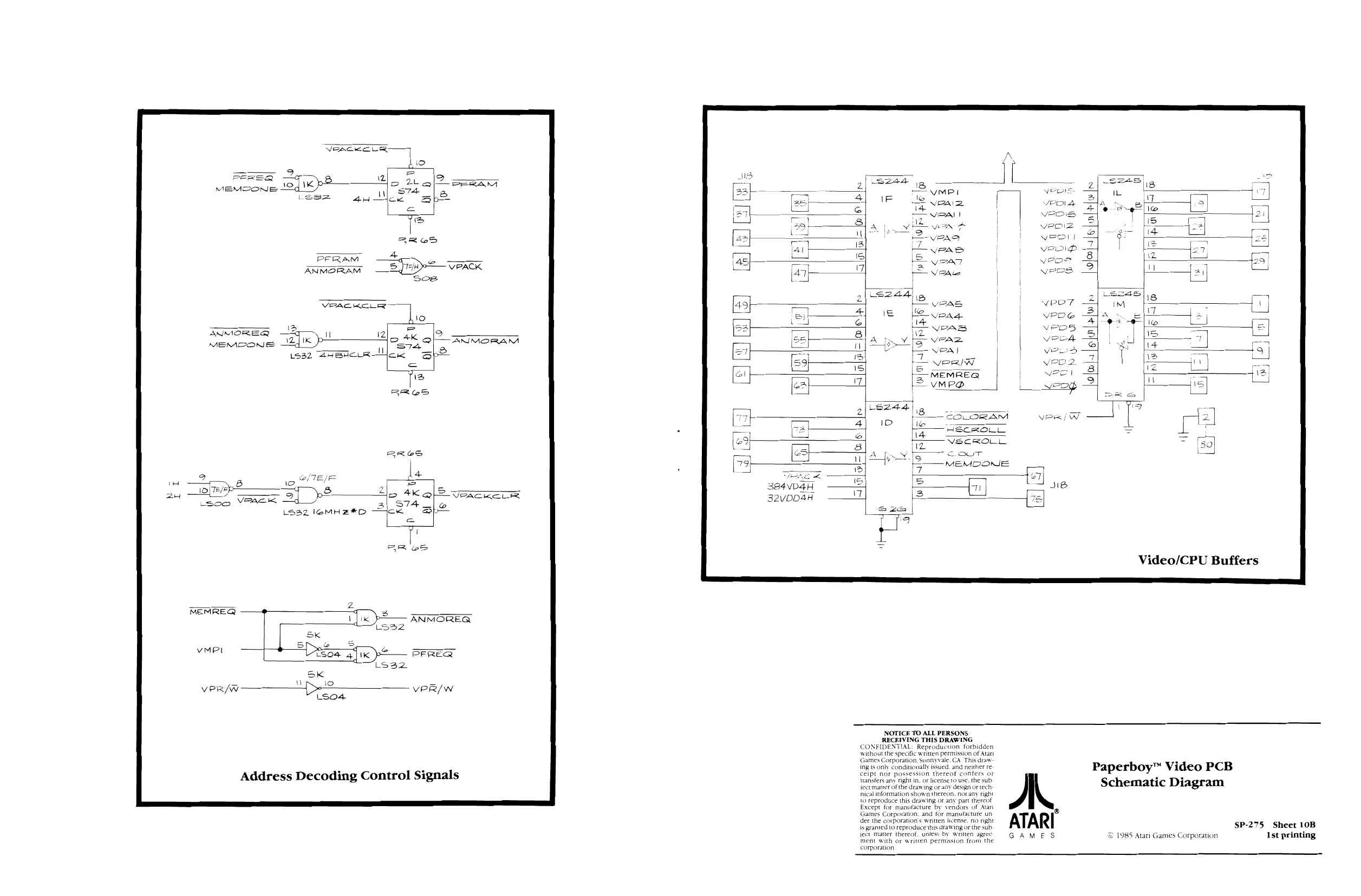
This page is a drawing, shown as the original scan.
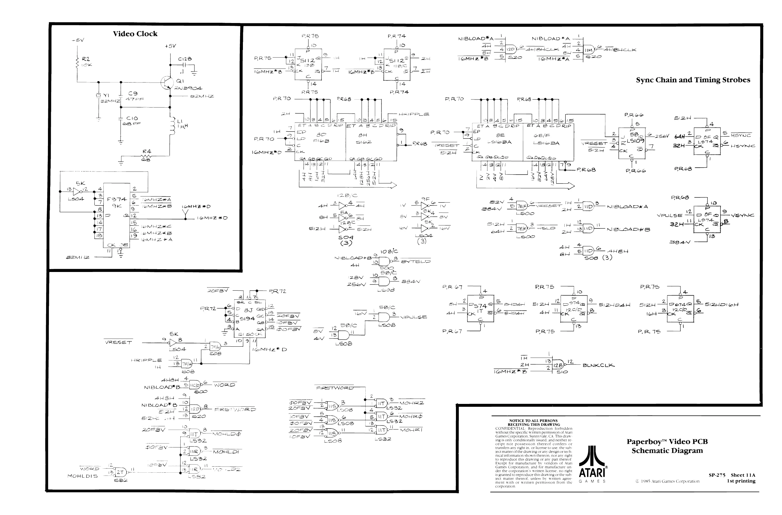
This page is a drawing, shown as the original scan.
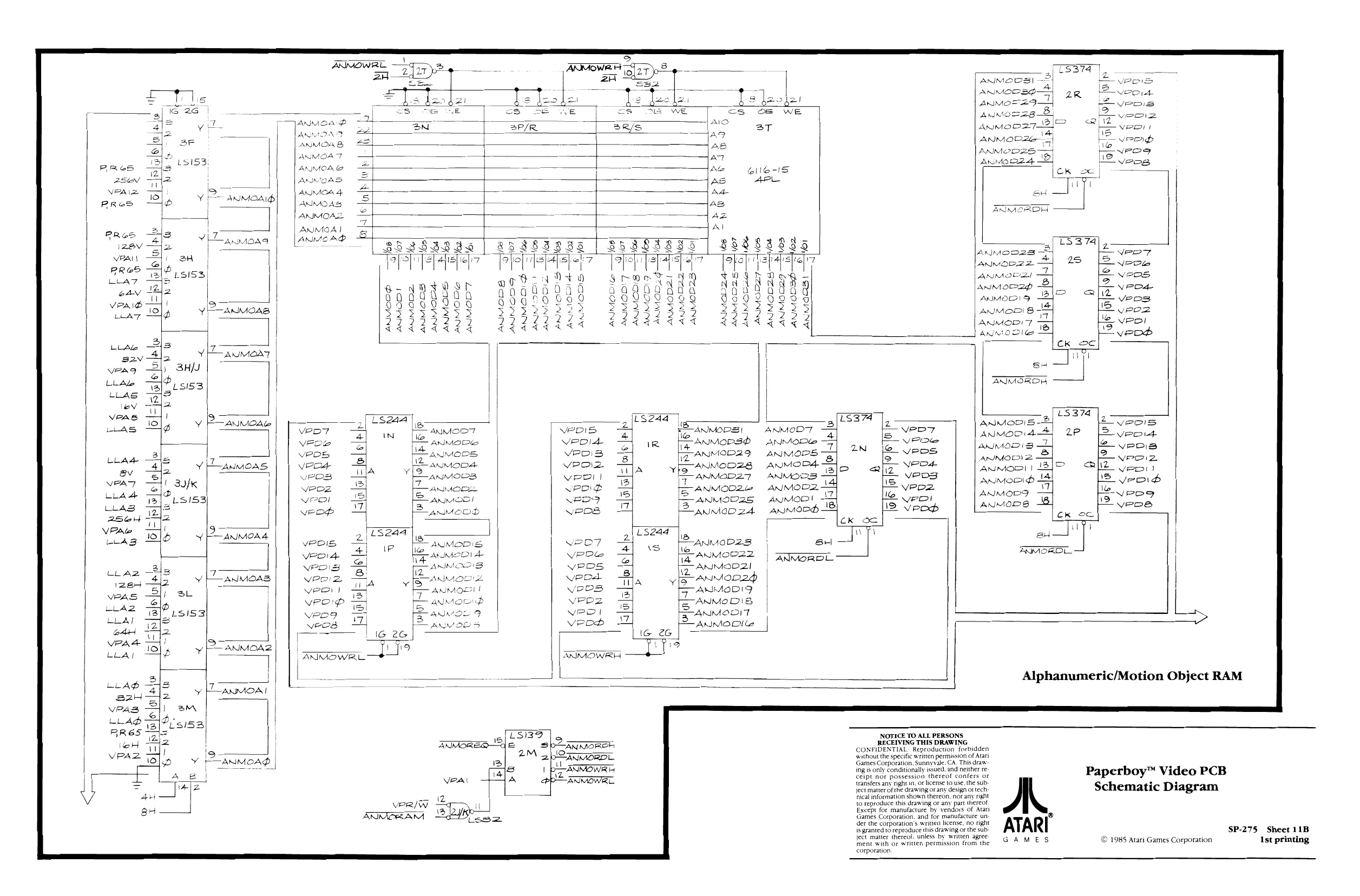
This page is a drawing, shown as the original scan.
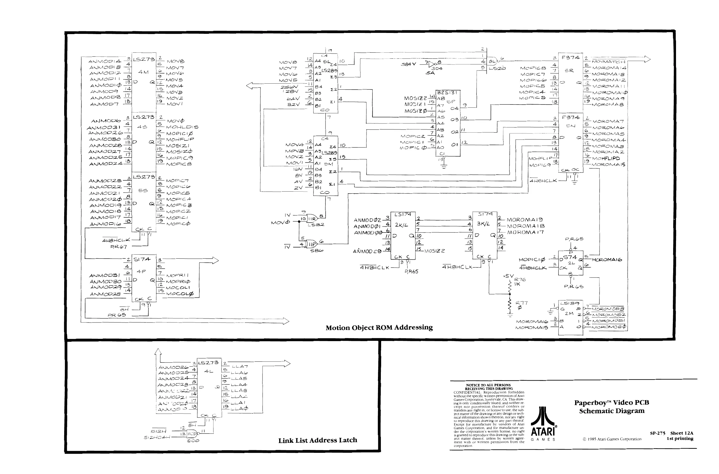
This page is a drawing, shown as the original scan.
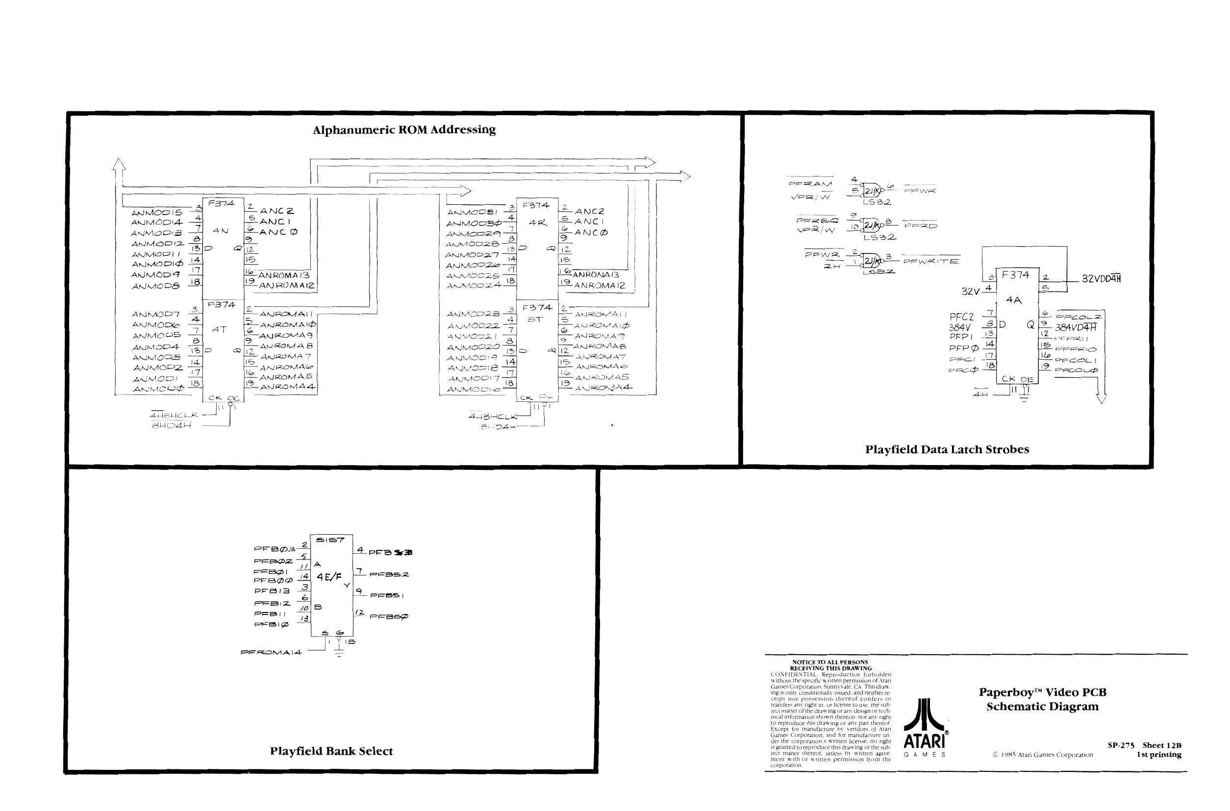
This page is a drawing, shown as the original scan.
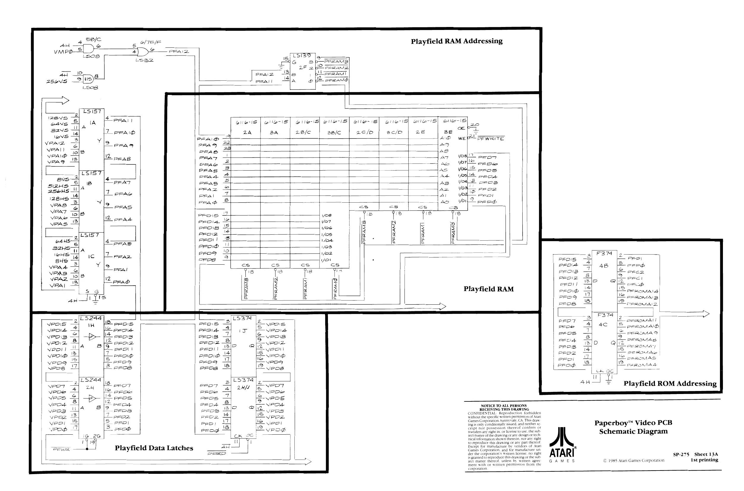
This page is a drawing, shown as the original scan.
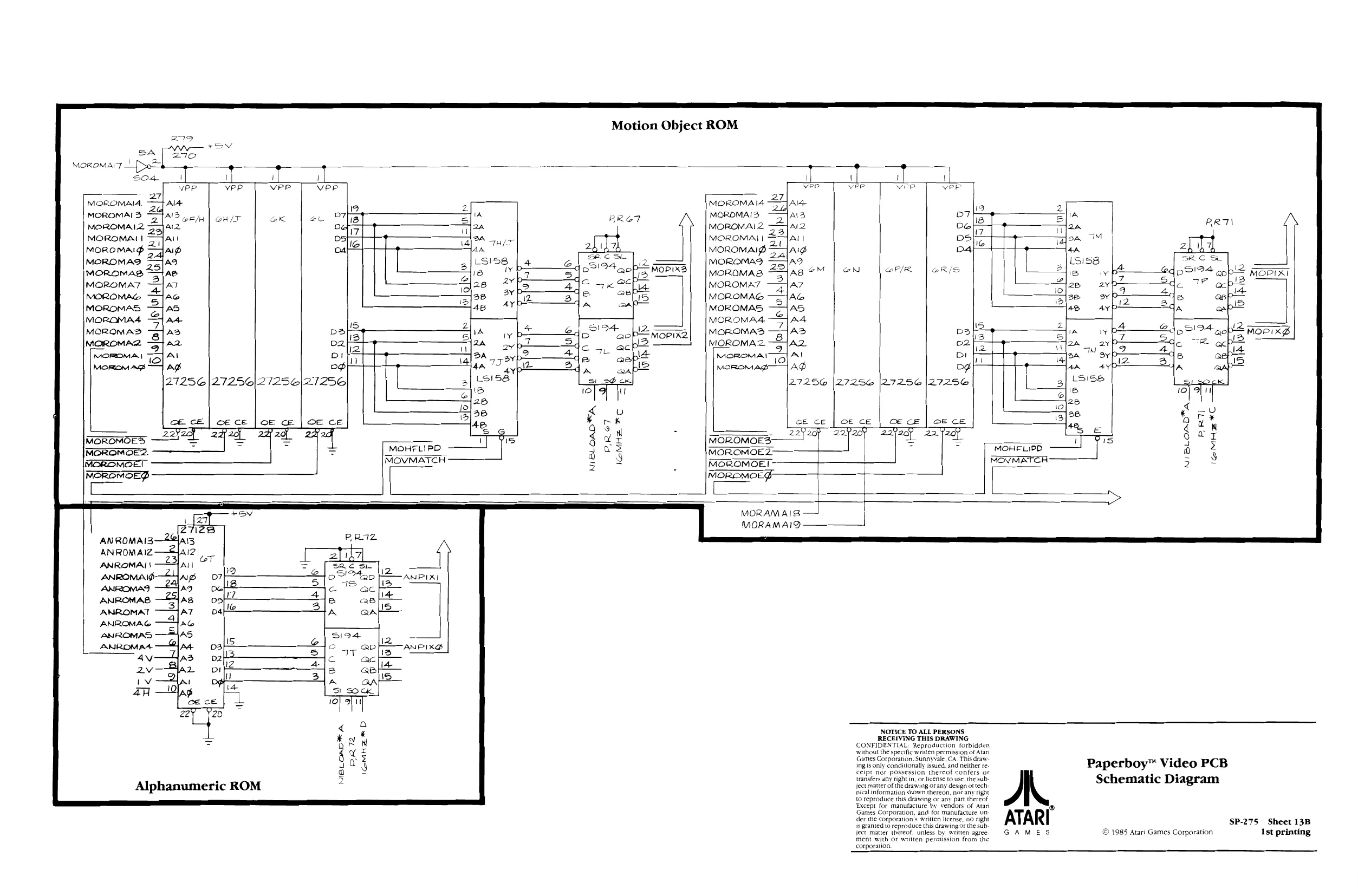
This page is a drawing, shown as the original scan.
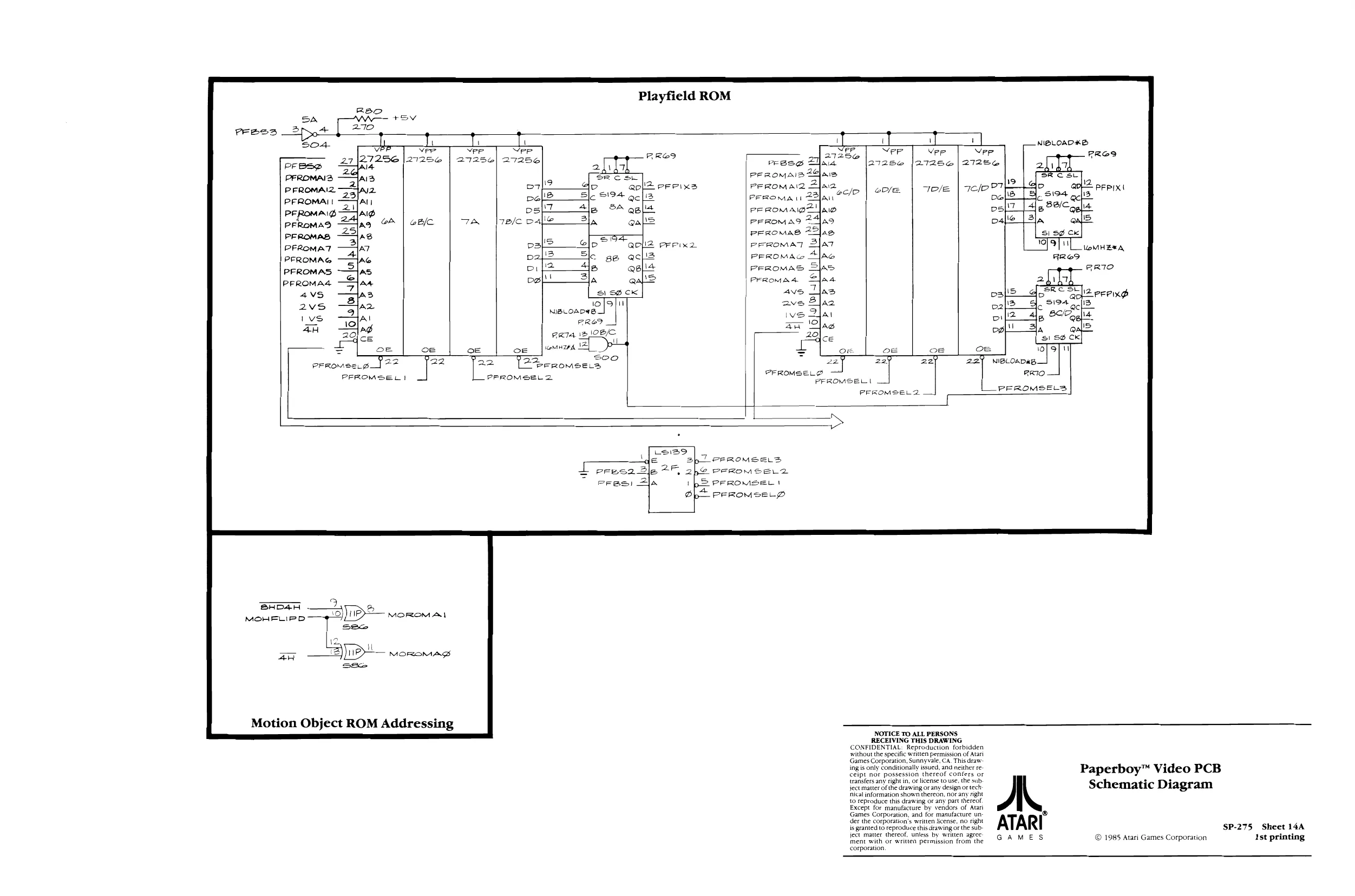
This page is a drawing, shown as the original scan.
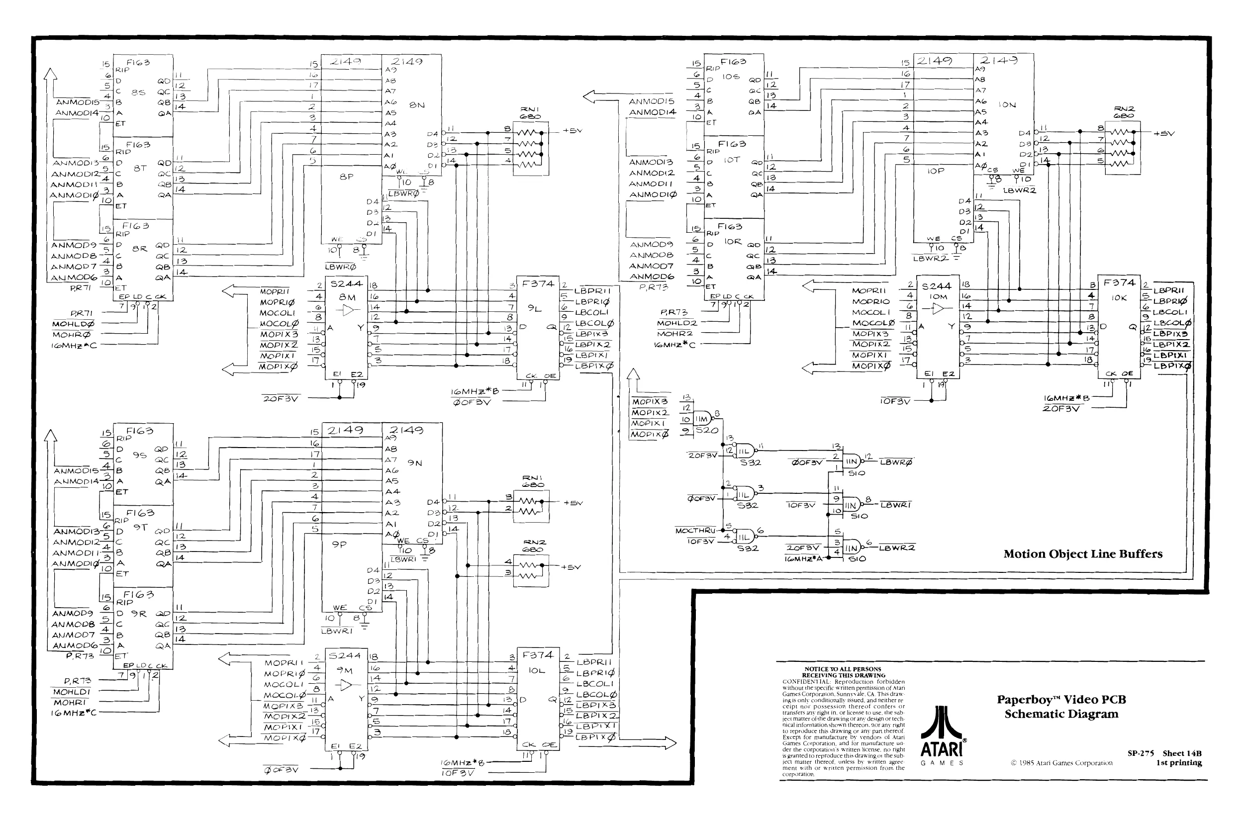
This page is a drawing, shown as the original scan.
This page is a drawing, shown as the original scan.
This page is a drawing, shown as the original scan.
This page is a drawing, shown as the original scan.
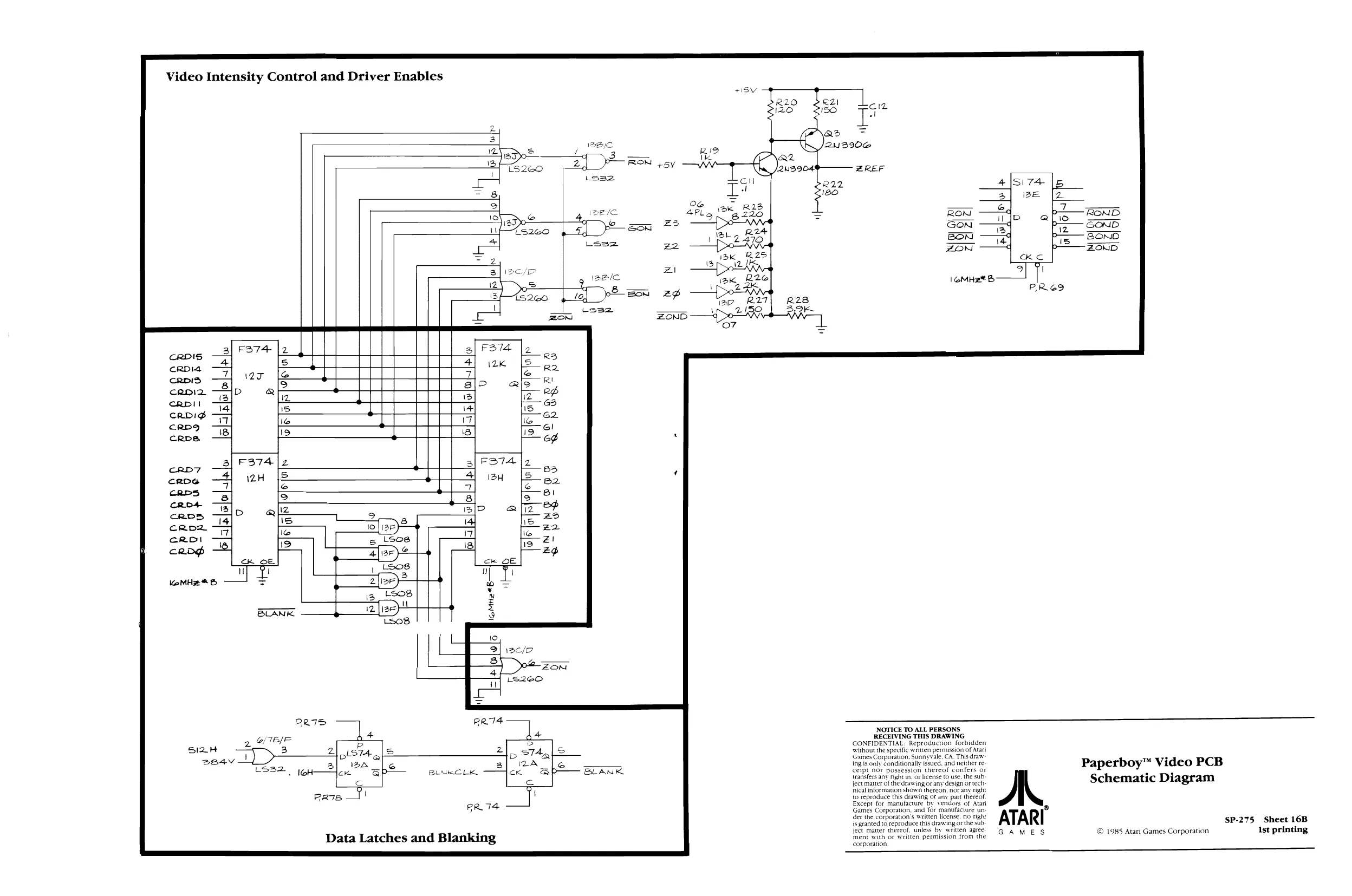
Video Intensity Control and Driver Enables
iy r im ep IoMH2*B—
A P S Zz S 2 = ote DB STA a IZA oe 3 V2. co CSS IeH ln BUNRCLIL a & co
erR74 —
Data Latches and Blanking
NOTICE TO ALL PERSONS RECEIVING THIS DRAWING CONFIDENTIAL: Reproduction forbidden ‘without the specific written permission of Atari ‘Games Corporation. Sunnyvale, CA. This draw ing is only conditionally issued, and neither re ceipt nor possession thereof confers or transfers any’ right in, or license co use, the subs ject matter of the drawing or any design or technical information shown thereon, nor any right to feproduce this drawing oF any part thereof Except for manufacture by Vendors of Atari Games Corporation, and for manufacture un: der the corporation's written license. no right fs granted to reproduce this drawing or the sub: ject matter thereof, unless by written agree ment with of written permission from the corporation’ AL
ATARI
GAMES
Paperboy™ Video PCB Schematic Diagram
© 1985 Atari Games Corporation SP-275 Sheet 16B Ist printing
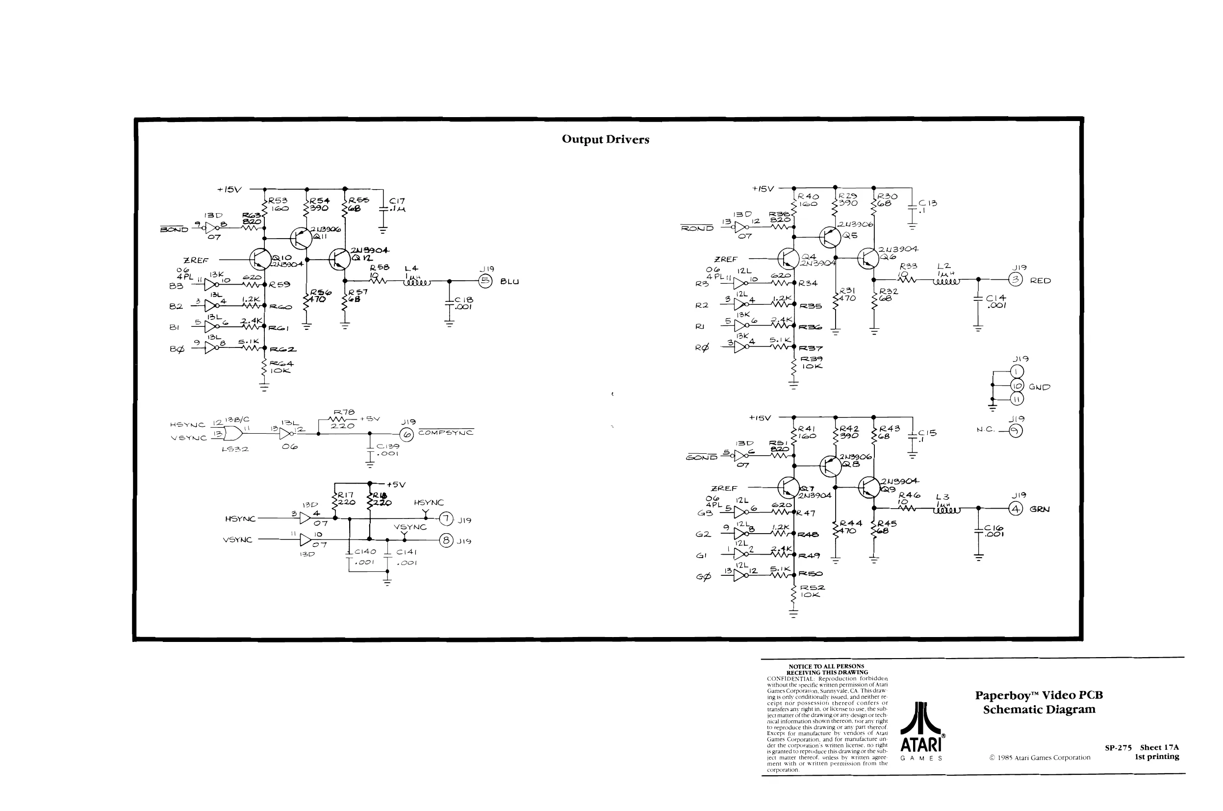
This page is a drawing, shown as the original scan.