Play Ball Model 4001A Operation and Service Manual
PlayBall! (prototype) (Williams, 1983) · Document · 58 pages · 41 sections · original scan
iHRHEeSSEeEeREee SBS Se SB ESE HE EEE
PLAY BALL
MODEL 4001A
AN ELECTRONIC GAME
BY
GREMLIN G3 INDUSTRIES, INCORPORATED
OPERATION AND SERVICE
MANUAL
PLAY BALL
ELECTRONIC WALL GAME by
GREMLIN INDUSTRIES, INCORPORATED
7030 Convoy Court San Diego, California 92111
OPERATING INSTRUCTIONS
and
SERVICE MANUAL
TABLE OF CONTENTS
INTRODUCTION-----~-------------------- page 1
UNPACKING & INSPECTION---------------- page 2
PLAY BALL DESCRIPTION------~-----~---- page 3
SYSTEM DESCRIPTION-------------------- page 5
INTEGRATED CIRCUIT CHARACTERISTICS----page 9
DETAILED CIRCUIT DESCRIPTION-~----~-~-~— page 19
POWER/SOUND BOARD-----~---~------=------ page 30
MAINTENANCE------~----—----------------— page 32
MAINTENANCE PROCEDURES---------------- page 33
PROGRAMMING & ADJUSTMENTS------------- page 40
SCHEMATICS === 99 nnnnnnnnnnnnnnn following pages
INTRODUCTION
PLAY BALL is an electronic game that makes extensive use of digital integrated circuits. This manual assumes that the maintenance technician possesses a general knowledge of solidstate circuitry and TTL digital integrated circuits. Any individual not knowledgable in this area should not attempt to repair the electronic portions of the game. IT SHOULD BE NOTED THAT ANY ATTEMPT TO REPAIR THE GAME IN THE FIELD WITH- OUT THE EXPRESS CONSENT OF THE FACTORY WILL IMMEDIATELY VOID THE WARRANTY!
NEVER replace any component with anything other than an EXACT replacement part. This includes LAMPS, TRANS- ISTORS, INTEGRATED CIRCUITS, and the like.
LAMPS used in this game are #1813, which operate at 14.4 volts, 100 ma. and #756 lamps which operate at 14.4 volts, 80 ma. NEVER use a lamp that operates at a lower voltage or higher current. To do so will very likely damage the circuitry in the game.
DO NOT use metal objects (screwdrivers, pliers, etc) around the lamp sockets with the game turned "ON". The outer shell of the sockets have voltage on them, and shorting them to each other or to other points on the game will damage the circuitry.
DO NOT replace the fuse with anything other than the proper value. A blown fuse indicates an overload condition within the game. Replacing the fuse with a larger value can cause severe damage to internal components if an overload occurs.
ALWAYS consult the manual before attempting any repairs.
CORRESPONDENCE regarding this game should be addressed to:
GREMLIN INDUSTRIES, INCORPORATED 7030 Convoy Court San Diego, California 92111
Phone: 714~277-8700
UNPACKING AND INSPECTION:
The PLAY BALL Game is normally shipped in two packages, one containing the game main frame and the other package containing the Coin Box, Transmitter, and accessories.
Both boxes should be opened immediately upon arrival and inspected for freight damage. It is advisable to connect the game for operation and determine that it is operating properly, as some freight damage can occur within the main frame and not be immediately evident during a cursory visual inspection.
If damage has occurred during shipment, the recipient should immediately file a damage claim with the carrier. Filing a claim will protect the recipient from bearing the full cost of any repairs that may arise from the damage.
Any game or accessory claimed to be defective must be returned to GREMLIN INDUSTRIES, INC., 7030 Convoy Court, San Diego, California, 92111, transportation charges prepaid. The game will be repaired and returned to the customer, transportation charges prepaid, if still within the warranty period. If the game is found to be damaged by misuse, improper attempts at repair, or abuse, it will be returned to the customer with transportation and repair charges billed.
In the instance of a defect of sub-assemblies or assemblies manufactured by others than GREMLIN INDUSTRIES, every effort will be made to assist the customer in obtaining satisfaction from the original manufacturer.
PLAY BALL DESCRIPTION
The PLAY BALL electronic wall game, Model 4001A is a single, wall-mounted unit that needs only an external coin box and transmitter/controller to operate. Both of the latter units are supplied with the game.
Within the main frame of the game assembly is a large (2.5 ft. by 5 ft.) printed circuit board, which contains plug-in provisions for the POWER/SOUND board and the LOGIC board. Additionally, a receiver module is incorporated to receive and process the signals transmitted from the hand-held transmitter control.
The transmitter/controller is a standard, tone-modulated 27 MHz radio transmitter. The only control necessary for its operation is the top-mounted push button that is actuated to play the game.
The coin box provided with the game is a Quarter Rejector type that causes a switch contact closure with each coin inserted. Each coin activates the circuitry in the main frame and allows a game to be played.
The game is played in the following manner: Two players compete in PLAY BALL, each taking turns at the control box that enables them to play from any place in the room.
A coin is deposited and the game activates, allowing the transmitter control box to initiate action.
The first player watches the scoreboard, on which pitch selections are alternating. He has a choice of a Fast Ball, Curve, Slider or Change Up. He depresses his control box button, putting the animated pitcher into action and an electronic "ball" travels toward the batter. Releasing the control box button starts the bat swing.
Just as in an actual game, the player must time his swing to make contact with the ball as it travels across the plate. Just how accurately he does so determines what kind of a "hit" he gets and how many points he scores. A Home Run scores 4 points, a Triple 3 points, a Double 2 points, and a Single is awarded 1 point. If he hits a Foul Ball, no points are scored, and if he misses the ball completely, a Strike is called and his opponent is awarded 1 point.
When the ball is hit, a realistic bat sound is emitted
and the lighted, electronic ball flies toward the outfield. When a Home Run is hit, a rousing crowd cheer, complete with whistles, is sounded.
A Free Game is awarded when a preselected number of Home Runs are hit during the period of a game. This feature may be inhibited for areas where free play is prohibited.
PLAY BALL is internally programmable. The speed of the ball is controlled by a master potentiometer located on the Logic Board. Also on the Logic Board is a potentiometer to control the sequencing speed of the Pitch Selection circuitry.
On the side of the game is a switch by which the players may program the game to either Major League speed or Minor League speed.
The length of the game is controlled by score. The score at which the game ends is internally selectable by means of jumpers provided on the Logic Board. The game may be ended on any increment of 10, up through a total of 70 points.
SYSTEM DESCRIPTION
PLAY BALL is a digitally controlled, sequentially animated game. Digital integrated circuits control the rate, interval, and sequence of events.
Figure A is a block diagram of the game. The receiver output is applied to an "Input Processor" which determines whether or not a game is in play. If the "games counter" has not been activated by the coin box, the Input Processor will not allow the receiver output to continue through to activate the game. Thus, a game cannot be played until a coin is deposited in the coin box. .
If the games counter is not at "zero" count, the input Processor allows the receiver input to activate the game action. The input from the receiver is normally high (approximately +5VDC). When the transmitter button is depressed, the level goes low (ground potential). Releasing the transmitter button again allows the input level to go high. When the transmitter button is depressed, the falling edge of the receiver output causes the "Pitch Select" circuitry to stop its alternating action and apply a fixed voltage to the "clock" circuit. This voltage determines the frequency at which the clock oscillator operates.
The same falling edge of the receiver output starts the ball animation circuitry operating, and the ball is “pitched" at a speed determined by the clock frequency.
When the transmitter button is released, the rising edge of the receiver output signal causes the bat swing circuitry to activate, and the animated bat begins to "swing".
If the animated bat and ball coincide in their paths over the plate, the "Hit Gate" senses the coincidence and scores a hit. The accuracy of the coincidence determines which hit is selected by the "Hit Select" circuit (Foul, Single, Double, Triple, or Home Run). At the same time, the Hit gate determines how many points to award to the player.
The "Casey-Lefty Select" circuit switches between the two players alternately and awards the points to the proper player.
The Free Game circuit is energized after a specific number of home runs is hit during a game. Should that number be reached, the circuit inhibits the games counter and, at game end, a free game is awarded.
The "End-of-Game" circuit monitors the score, and when predetermined score (which is internally selectable) is achieved, the games counter is "stepped" down one count, and the game is ended. If the games counter is then at "zero" count, no further play is possible. However, if more than one game was registered, it simply steps down to the next game and, after a short delay, the score is reset to zero and the next game is started.
DIAGRAM SIMPLIFIED BLOCK
Free Game Counter Hit Select
Receiver
Games Counter
FIGURE A
N7404 HEX INVERTER
SCHEMATIC (each inverter) )
FIGURE 1
QUADRUPLE 2-INPUT
N7408 POSITIVE AND GATES
SCHEMATIC (each gate)
FIGURE 2
INTEGRATED CIRCUIT CHARACTERISTICS
GENERAL:
Digital integrated circuits possess a unique characteristic in that their outputs can assume only two states. They are either HIGH (output at a positive voltage level), or LOW (output at or near ground potential). While there are many types of digital integrated circuits of varying complexity, all must conform to this limitation: their outputs are limited to switching between two voltage levels, HIGH and LOW.
For the purposes of this discussion, only "TTL" (Transistor-Transistor-Logic) circuits used in GREMLINs' PLAY BALL game will be examined.
7404 HEX INVERTER: ----------------------------------------
Figure 1 illustrates an integrated circuit containing six simple inverter circuits. Each circuit functions simply to "invert" the state of the voltage applied to its input. If the input is LOW, the output will be HIGH. Conversely, if the input changes to a HIGH state, the output will immediately change to a LOW state. Thus, it "inverts" the signal applied to the input terminal. Inverters are used primarily to invert a signal that is of the wrong polarity to interface with, or drive, another circuit or device.
7408 AND GATE: --------------- eeon----------- + --
Figure 2 depicts a Quadruple 2-input AND gate, the 7408. In operation, the output of each gate will go HIGH only if both inputs are HIGH. Restated, the output will change to a HIGH state only when both input 1 AND input 2 are HIGH. It is therefore called an AND gate.
Consider a typical application: If input 1 remains at a LOW state, the output will be LOW and any changes at the other input will not affect the output. However, if input 1 then goes HIGH, it will allow the changes at the other input to appear at the output. Returning input 1 to the LOW state will again cause the output to go to the LOW state and inhibit any further signals at input 2 from being felt at the output. Thus, the signal at input 2 has been "gated" to the output by a signal applied at input 1. Hence the term GATE.
The PLAY BALL game uses several circuits of this type to gate signals on and off.
N7400 QUADRUPLE 2-INPUT PosiTivE
NAND GATE
oe iain
FIGURE 3
N7410 TRIPLE 3-INPUT POSITIVE NAND GATE
SCHEMATIC (each gate)
FIGURE 4
N DUAL D-TYPE EDGE-TRIGGERED
N7474 FLIP-FLOP
FIGURE 5
7400 _NAND GATE: ------------------------------------------
Figure 3 illustrates the 7400 Quadruple 2-Input NAND Gate. It operates exactly like the AND gate, but it performs the added function of inverting the output. Therefore, when both Input 1 and Input 2 are HIGH, the output will go LOW. A NAND gate can be thought of as an inverting AND gate.
Figure 4 shows a Triple Three-Input NAND Gate. All three inputs of each gate (Input 1 AND Input 2 AND Input 3) must go HIGH to obtain a LOW state at the output. A LOW at any of the inputs will maintain a HIGH condition at the output.
7474 "D"_BLIP-PLOP : ---- 7-72 n nnn nnn nnn nnn nnn nnn nnn
The circuit shown in Figure 5 is a Dual D-Type, Edge- Triggered Flip-Flop. It is a relatively complex circuit made up of several of the gates discussed above. It is conventionally shown as a "block" diagram with input and output functions designated as shown, and it operates as follows:
Input information is applied at the "D" input. This may be either a HIGH or LOW potential. The input is transferred to the Q output upon the positive transition of a pulse applied to the clock (CK) input. For instance, if a HIGH is applied to the "D" input, and held there, no change in the Q output will be noted until a clock pulse is applied to the CK input. When the positive edge of the clock pulse occurs, the HIGH felt at the input will be transferred to the Q output. Any additional clock pulses that occur while the "D" input remains HIGH will cause no further change. However, should the "D" input go to a LOW state, the positive transition of the next clock pulse will cause the Q output to go LOW.
The "D" Flip-Flop also has a Q (pronounced "Q-Bar") output, which simply provides an output that is always the opposite of the Q output. If Q is HIGH, Q will always be LOW, and vice-versa.
A "D" Flip-Flop also has two other inputs labeled "PRESET" and "CLEAR". These inputs may be used to set the outputs to a desired state. With both the PRESET and CLEAR inputs held HIGH, the circuit will operate normally. Ifa LOW is applied to the PRESET input, it will cause the Q output to go LOW. Conversely, if a LOW is applied to the CLEAR input, it will cause the Q output to go HIGH. It is
N7490
DECADE COUNTER
LOGIC TRUTH TABLES
BCD COUNT SEQUENCE (See Note 1) RESET/COUNT (See Note 2)
RESET INPUTS OuTPUT NOTES:
| D | BLA | Roi2) | Rota) | Rota | Roi) | © © BA | 1. Output A connected to input | |||||
| Q | 0 | 0 | 1 | 1 | 0 | x | [oovoo | BD for BCD count. | |
| 0 | olo | 1 | 1 | 2. X indicates that either a logi- | ||||
| 0 | 110 | x | ° | ooae | cal 1 of a logical O may be pre- | |||
| i) | 1 | q | x | x | 1 | 1 | 10071 | sent. |
| : | ae | x | ° | x | ° | COUNT | 3. Fanaut from output A to in- | |
| 3 | ; | é | ae | x | o | x | COUNT. | put BD and to 10 additional |
| 0 | 1 | 1 | Series 64/74 loads is permitted | |||||
| & | ey | ° | x | x | ° | count | ||
| 1 | oO | 1 | x | 0 | o | x | COUNT |
FIGURE 6
TRUTH TABLE (See Notes 1 and 2)
LOGIC
OUTPUT OUTPUT
count COUNT NOTES:
| oc | BA | o | cc | B | A | 1, Output A connected to input B. | |||
| 0 | 0.0 | 6 | O | 3 | a | ar | 2. To reset all outputs to logical 0, | ||
| 1 | 0 | 0 | oOo | 41 | both Rai) and Agia) inputs | ||||
| 2 | 0 | o | 1 | © | (2 | ns | must be at logical 1. | ||
| 3 | 0 | 0 | 14 | 4 | ul | 1 | 0 | 4 | 1 |
| 4 | o | 1 | 0 | 0 | 12 | + | 4 | 0 | 0 |
| 5 | o | t | oO | 4 | |||||
| 1 | 1 | 1.0 | |||||||
| 6 | eo | 1 | 1 | 0 | 7 | ! | |||
| 7 | o | o4 | 4°41 | 14 | ee | ||||
| 8 | 1 | 0 | 0 | 0 | 15 | ,o4 | 44 |
FIGURE 7
It should also be noted that clock triggering occurs on the positive-going transition of the clock pulse, Thus, the 7474 is called an "edge-triggered" Flip-Flop. Triggering occurs at a voltage level of the clock pulse and is not directly related to the transition time of the positivegoing pulse. After the clock input threshold voltage has been passed, the data input "D" is locked out, and any change in the "D" input after that time will not affect the outputs until the next positive-going transition of the clock pulse.
7490 DECADE COUNTER: ~-------------------------------------
Figure 6 illustrates a a 7490 decade counter which is a circuit composed of several internally connected Flip- Flop circuits. They are connected in a manner that allows division of the input signal frequency by a factor of 10. In addition, the state of the count is provided at four digital output pins, which are the outputs of the four internal flip-flop circuits.
Figure 6a shows the output configuration of these four output pins as the number of input pulses applied goes from one to ten. These four outputs provide "Binary-Coded Decimal" (BCD) information which may be decoded by additional circuits for display as numbers or sequential events.
The 7490 counter has gated direct reset lines which inhibit all count inputs and returns all outputs to a LOW (Logical 0) state (Pins 1 & 2 on the IC) Additional reset lines are provided at pins 6 & 7 which will preset the counter to a BCD 9 count for certain applications. With both reset circuits (Pins 1, 2, 6, and 7) held LOW, the counter will count normally.
7493 4-BIT COUNTER :~-~------~ 99-22 nn nnn nnn nnn nn nn nn Figure 7 illustrates the 7493. This circuit is similar in operation to the 7490 decade counter, except that it has a count capability of 16. That is, it will divide the input frequency by 16 and provice a BCD output to indicate the state-of-count.
The 7493 consists of four internally connected Flip- Flops which provide proper count capability. A gated direct reset line is provided which inhibits the count inputs and simultaneously returns the four flip-flop outputs to a logical 0 (LOW). Figure 7a shows the logic truth table associated with the 7493 for a count sequency of 0 through 15.
‘This counter is used primarily for frequency division in the PLAY BALL game.
BCD-TO-SEVEN SEGMENT
DECODER/DRIVER N7448
FOMENT IDENTIFICATION
[MUMERICA, DESIGUATIONS RESULTANT OBPLAYS. FIGURE 8 N7475
TRUTH TABLE
QUADRUPLE BISTABLE LATCH
before ciock pulse.
- they = bit time after clock pulse NOTES:
‘These voltages are with respect to network ground terminal. th+1 (Each Latch) ry LOGIC. fn D
FIGURE 9 N74154 =2s +e o -S ws = =} fe i]
TRUTH TABLE
Qlrrrrrrrrrrrrrerrarrs F[rxurrrrrrrrrrrrsizrrr:r Slrrrrrrrrrrrrrarrrrr S[rerzzrrrzrrzrrrsirrsrrrr Pa rTIrrrrrrrrrsarrrrrigrr Slerrrrrrrrrstyrrzrzrrer Plrrrrrrrrtrixrrxrrrr4r3rr Blejzzrzrrrrrsrsrrrrrrsrr B(Sjzrrrsertsarcagrrrrrrrir Plelrrerrrsizrererrrerre @lrrrrlsarrrrrrrirrr3r3r:r S\rrrrarrrrrrrrrrrrrs @lrrlsarrrrrrrrrrrrrrer Slrtarrrrrrrgrrrrrirr: “|lEskEPE DE Irrirerirsrs a OfarcrcrrrrrrrrrrgLririczg {ara rararsrarararxxx m@fssrrasrrgsarrsirrxxx BMi9j/saansasvsIrrrsasiasarrrmxx.x glols2sssasarrrrerrrxxx "|Slo ass assesasaasaatar Gloss s sass aassaanaaarer
H = High, L = Low, X = Irrelevant ~14- FIGURE 10
7448 BCD-TO-SEVEN SEGMENT DECODER/DRIVER:----~-----------~
The 7448 integrated circuit that is used to decode a BCD output such as that from the 7490 previously discussed is shown in Figure 8. This circuit converts the four outputs of the BCD counter into seven outputs which, when used to drive a Seven-Segment Readout, will display in numerical form the count configuration of the counter and change it into a readable numerical form. The numerical designations of the resultant display are shown in Figure 8a.
7475 QUADRUPLE _BISTABLE LATCH:
The 7475 latch circuit is shown in Figure 9. This device contains the equivalent of four flip-flops that operate similar to the 7474 previously discussed. The flip-flops here are not edge-triggered, however. Information present at the data (D) inputs is transferred to the Q output when the clock is HIGH, and the Q output will follow the data input as long as the clock remains HIGH. When the clock goes LOW, the information (that was present at the data input at the time the transition occurred) is retained at the Q output until the clock is permitted to go HIGH.
The 7475 is commonly used between a decade counter circuit and a decoder/driver circuit such as the 7448. In this application the clock input is held LOW, retaining the previous display, while the counter is advancing. When the desired count is reached, the clock on the 7475 is allowed to go HIGH and the information from the counter is then allowed to be transferred to the decoder/driver, changing the presentation to the new resultant display. This eliminates the distraction of seeing the numbers randomly cycling until the proper count is reached and it also adds versatility to the circuitry.
74154 4-LINE to 16-LINE DECODER: ----~--------------------
Figure 10 depicts the 74154. This circuit decodes the 4 BCD inputs applied to it from a 4-bit counter (similar to the 7493, for instance) into sixteen individual outputs. Thus, for every possible state of the BCD count of sixteen, there is one output of the 74154 that will change to the LOW state. Figure 10a shows the truth table for the device.
In operation, if a counter input were applied to the circuit and allowed to count normally, the output of the 74154 would progressively sequence from 0 to 15, and continue to repeat the sequence.
~-15-
‘NOTES: A. Clear overrides load, date, and count inputs,
- When counting up, count-down input must be high; when counting down, count-up input must be high. FIGURE 12 COUNT UP
‘COUNT DOWN
SEQUENCE IAUSTRATED curar
toa
para, | L
canny
poRFOW N7442
N74193 =s00+4004+004400/0 TRUTH TABLE
BCD INPUT
c
@ o oO oO
co) oO oO o ° = =. ad o m = = oS m oe i—} ao m =z
mOo20+0+0+0+040-0]/5 DECIMAL OUTPUT
al
SYNCHRONOUS 4-BIT BINARY UP/DOWN
COUNTER WITH PRESET INPUTS
FIGURE 11
Figure 11 illustrates the 7442. It is generally used in decoding and logic conversion applications. It decodes a four-bit BCD number (from the 7493, for instance) and converts it to l-of-10 output configuration.
The 7442 is used in the PLAY BALL game to provide sequential animation from a binary counter.
The circuit shown in Figure 12 represents the 74193. This counter has a capability of counting from 0 to 15 (as did the 7493 previously discussed), but it possesses the capability of counting in either direction. There are two separate inputs (pins 4 & 5), one for "count up" operation, and one for "count down" operation.
Count operation is triggered by a low-to-high level transition of either count (clock) input. The direction of counting is determined by which count input is pulsed while the other count input is held HIGH.
A CLEAR input is provided which forces all outputs to the LOW state when a HIGH level is applied. The CLEAR function is independent of the count inputs and overrides any other input.
The counter has a BORROW and CARRY output as well. The CARRY output provides a pulse in the "count up" mode to indicate when full count has been reached. Conversely, the BORROW output provides a pulse in the “count down" mode to indicate when "0" has been reached in the countdown sequence.
The 74193 has LOAD inputs which allow it to be "loaded" to any preset state by applying input signals to the 4 inputs and allowing the LOAD input to go HIGH. The respective outputs will then assume the signal level of the inputs. Count inputs will then cause the counter to sequency properly from this pre-selected configuration. Figure 12a is a sequence diagram of a typical CLEAR, LOAD, and COUNT operation.
The 74193 is used in the PLAY BALL game in two places where a reverse in count direction is necessary: the game counter and the ball flight counter. The LOAD inputs are not used in the game.
NE555 TIMER CIRCUIT: --------------------------------------
The NE555 is properly called a LINEAR integrated circuit because not all of its inputs are digital two-state
levels. The 555 is a highly stable controller capable of producing accurate time delays, or oscillation. Additional terminals are provided for triggering or resetting if desired.
In the time delay mode of operation, the time is precisely controlled by one external resistor and capacitor. For stable operation as an oscillator, the free-running frequency and the duty cycle are both accurately controlled with two external resistors and one capacitor.
The circuit may be triggered and reset on falling, (negative-going) waveforms, and the output structure can source or sink up to 200 ma or drive TTL integrated circuits.
This circuit is used in the game as both a timing device and a controlled oscillator.
DETAILED CIRCUIT DESCRIPTION
The signal from the coin box is applied to pins 65 & 66 on the logic board. A ground is normally held at pin 66, keeping pin 3 of U-24 (all IC's are designated as U-XX) HIGH. When a coin is deposited, the ground is removed from input pin 66 and applied at pin 65, which causes pin 3 of U-24 to go LOW. This, in turn is felt at the "Up Count" (pin 5) input to U-29, an UP/DOWN COUNTER. The BCD output of U-29 is decoded into 10-line form by U-28, inverted by U-49 and applied to driver transistors 45 through 48. When a single coin is inserted, GAME 1 will light on the display panel. More coins will cause additional games to be sequentially illuminated.
The reset input of U-29 (pin 14) is held LOW for normal counter operation. However, when the game is first turned on, a HIGH input is felt at this terminal due to the gate (U-32) that is attached to it. When power is applied, pins 12 & 13 of U-32 are LOW and Pin 11 is HIGH, which holds counter U-29 in RESET. As capacitor C-16 charges to a HIGH level, the gate output at pin 11 goes LOW and the counter may then operate normally. This assures that the counter will always come up on "0" games when power is applied to the circuitry.
PLAY INHIBIT: ------~-~----------------~---------------------
When counter U-29 is at "0", pin 1 of U-28 applies a LOW to pin 1 of U-21, an AND gate. Pin 3 of U-21 therefore goes LOW and holds the D Flip-Flop, U-6, in the CLEAR mode until this signal is removed. U-6 is the input processor for the receiver signal and when in the CLEAR mode, it will not allow any signal to pass. Thus, a game cannot be played at this time. If a coin is inserted, the CLEAR input will go HIGH, allowing U-6 to operate normally, and a game may be played
The ball speed control is comprised of oscillator U-47, a control gate (Part of U-24), a one-bit counter (U-5), decoding gates U-37, and transistors 59 through 66.
The master clock oscillator that controls the speed and sequence timing for the game is U-38, an NE555 connected as an oscillator. Its natural period of oscillation
is controlled by capacitor C-1 and the resistance of R-11l and R-12. The NE555 also has an input at pin 5 that allows the frequency to be changed by the application of a DC voltage. Changes in voltage at this point will cause changes in the output frequency of U-38. The voltage is changed by the resistive divider that is tied to pin 5, (made up of R-5 through R-9). When one of the transistors (59 through 62) is turned on, it essentially connects one side of its collector resistor to ground, thus establishing a voltage divider between that resistor and R-9. This yields a particular voltage at pin 5 of U-38. When the transistor turns off and another of the four transistors turns on, a different resistor is placed into the divider and the voltage applied to pin 5 changes. Thus, if the action of sequentially selecting transistors 59 through 62 continues, the output frequency of U-38 will change accordingly.
The switching action at the transistors is controlled by the decoded outputs of U-5, a D-type Flip-Flop that is connected as a two=bit counter. Reference to the integrated circuit data will show that there are two independent Flip- Flop circuits in a 7474 IC. These may be hooked up in such a manner that they will "toggle", or count. When the two flip-flop circuits are then connected in series, they posses the capability to count, or divide, by 4. U-5 is connected in such a configuration. U-37, containing four "AND" gates decodes the counter output into a serial output (0-1-2-3 and applies signal to the switching transistors (59 through
- previously discussed.
It should be noted that the counter and decoding circuits also drive four additional transistors, 63 through 66. These transistors operate the lights on the game display ("Curve", "Slider", "Change Up", and "Fast Ball"), which are associated with the four ball speeds that may be selected.
U-47 is the oscillator that controls the rate at which the above changes occur. Potentiometer R-34 allows this rate to be internally adjusted. The output of U-47 is applied to the U-5 counter through a gate. When this gate is OPEN, the oscillator output is allowed to proceed to Pin 3 of U-5. However, during a game, once the ball is “pitched" the master clock U-38 must not be allowed to continue changing frequency. Consequently, when the receiver input indicates that the transmitter button has been depressed, and U-6 Flip-Flop "latches", pin 5 of U-24 goes LOW and all further oscillator (U-47) output is inhibited passing through to the counter. The counter therefore stops and a constant DC potential is applied to the master clock. The pitch nomenclature on the game front
panel also stops changing and indicates the particular "pitch" that has been selected.
Once the pitch and play action has been completed, a CLEAR pulse is applied to pin 13 of U~6 and the gate U-24 is reopened. This causes the oscillator to resume its sequencing action. BALL ANIMATION:~-------- nanan nn --------- == --- $= === 2 ===
Ball animation is achieved by sequentially energizing a series of lamps, causing an illusion of ball "movement" as it is pitched and hit during a game. This is accomplished by using a 74193 UP/DOWN counter and a 74154 4-Line-to-16-Line Decoder. The 74193 counts 0 through 15, but its output is in BCD form. The 74154 converts the BCD into a sequential 16 Line output.
It would appear that the above would limit the number of lamps that could be controlled to 16 in number, however, such is not the case. When counter U-12 begins to count, the output from the 74154 begins to sequence from count 0 through count 15. When count 15 is reached, a pulse is applied from pin 17 of U-41 to pin 3 of U-18. This causes Flip-Flip U-18 to toggle. The U-12 counter continues to count and the 0 through 15 count sequence is repeated. However, the same lamps on the game front do not illuminate, because as U-18 toggled after the first sequence it changed the Power Control output at connector Pins 85 and 86.
POWER CONTROL: -----~------------ -e------------- ~~ ------- an
Figure 14 illustrates the operation of the POWER CONTROL CIRCUITS. The transistors should be assumed to be sequentially turning “on" and "off", 1 through 16. If the output from IC-1 is HIGH and Ic-2 and IC-3 are LOW, only SCR-1 will be on. Thus, aS the transistors sequence from 1 through 16, only the "A" lamps in the collector circuits will be illuminated. If, during the next sequence, IC-2 is HIGH and IC-1 and IC-3 are LOW, SCR-2 will be on and only the "B" lamps will be illuminated. This is exactly the action that occurs during a ball "pitch" in the game. The first half of the ball trajectory (16 lamps) is controlled by an SCR POWER BUSS. When the counter reaches its maximum count of 15, the flip-flop, U-18, changes the Power Buss when it toggles, and the counter repeats its count again. This time however, a different power buss is energized, and the lamps that constitute the last half of the ball pitch trajectory are illuminated, completing the "Pitch".
When a HIT is registered, the UP/DOWN counter
I4V RECTIFIED
FOWER
SUPPLY SIMPLIFIED POWER CONTROL SCHEMATIC MODEL 400/A
FTGURF 14
reverses its count and sequences the transistors in the opposite direction. This would normally cause the ball to retrace the path it had previously used, but the POWER CONTROL again takes over and IC-3 turns on Scr-3 and only the "C" Lamps will illuminate, showing the ball arcing into the air after being hit.
PITCH INITIATION: -------~-----~--------------------------7----
When the transmitter button is depressed, the receiver applies a LOW input to pin 12 of U-6. This causes a HIGH to appear at pin 8 and a LOW at pin 9. As pin 8 makes the transition from LOW to HIGH, this is sensed at pin 3 of U-8, causing pin 5 of U-8 to go HIGH. This is applied to pin 12 of U-15 control gate. The other input to the control gate comes from the Master Clock, U-38 through U-7, a divide-by-16 counter. The frequency from this counter is the sequence rate at which the ball will be stepped in its trajectory. The gate U-15 is normally closed, but when Pin 12 goes HIGH (transmittér button depressed), the gate opens, and the signal is allowed to pass into Pins 12 & 13 of U-9.
U-9 is connected to act as a simple inverter and applies the signal to the UP/DOWN control U-1ll. U-11 is normally in the UP mode, so an output is felt at pin 6 of U-11 and applied to pin 5 of U-12, the UP/DOWN counter, and the pitch is initiated and the input signal steps the ball toward the batter.
PITCH STOP :---------~-----~--------------- - 5 - $5 =
The above description showed that Gate U-15 (pins ll, 12, & 13) was opened when The "D" Flip-Flop was "set" by the Transmitter initiation. Resetting the Flip-Flop (U-8) is accomplished by applying a LOW input to pin 1, (the CLEAR input). This Signal is derived as follows:
Pin 17 of U-41 goes LOW on the count of 15 and this signal is applied to Pins 9 & 10 of U-17, which is connected as an inverter. The output of U-17 is a positive pulse that is then applied to NAND gate U-17, pin 12. However, during the first 16-line sequence of U-41, U-18 is set in a mode that has pin 5 LoW. This is also applied to Gate U-17, pin 13, thus holding that gate CLOSED. After the first sequence is completed, and the counter begins to repeat the 16-line sequence, U-18 is triggered at pin three so that pin 5 goes HIGH. Thus, when the LOW pulse appears at U-41, pin 17 during the second sequence, it will be inverted into a HIGH pulse and applied to pin 12 of U-17, which is now an OPEN gate. It will pass through the gate, and is applied to pin 10 of U-10, an AND gate. (It should be remembered here that this neg-
ative (LOW) pulse appears only after the second count cycle of U-12.) This LOW signal is coupled through the AND gate and applied to U~-8, Pin 1 (the CLEAR input). This resets the Flip Flop, and closes the gate at U-15, pin 12, thus inhibiting any further input to the UP/DOWN counter, and stopping all ball animation.
"STRIKE" :----------------------------------------------------
When the pitch sequence has been completed, and a HIT has not been registered, the following occurs to register a "STRIKE":
Pin 6 of U-8 goes negative at the time of pitch initiation, and stays LOW throughout the pitch sequence. At the end of the pitch sequence, pin 6 goes HIGH. This is felt at pins 9 and 10 of U-15, which is connected as an inverter. Pin 8 of U-15 thereupon goes LOW. The leading edge of this negative transition is differentiated by capacitor C-4 and this differentiated pulse serves to trigger U-31 (an NE555 connected as a one-shot multivibrator). This pulse causes pin 3 of U-3l to go HIGH and remain there until the circuit times out (approximately 3 seconds). The positive pulse is also applied to pin 1 of U-10. Pin 2 of U-10 is also HIGH when no hit has been registered, so the pulse is allowed through the gate and turns on Silicon Controlled Rectifier (SCR) 1, which lights the front panel display "STRIKE".
When Timer U-31 times out and pin 3 goes back to a LOW condition, the negative transition is differentiated by capacitor C-6 and applied to pin 1 of U-6, resetting that Flip-Flop. This, in turn, re-opens gate U-24 and the pitch nomenclature begins alternation again. Additionally, the negative transition that occurs at pin 5 of U-6 is differentiated by capacitor C-12 and applied to pin 9 of U-11. This assures that the UP/DOWN Latch is set in the UP mode and is ready for the next pitch.
BAT SWING:--------------------------------------------------
Input Processor U-6, Pin 9 goes LOW when the transmitter button is depressed and Goes back HIGH when the button is released. This positive-going transition serves to trigger "D" Flip-Flop U-8. When this flip-flop latches on, Pin 9 goes HIGH and Pin 1 of U-15 follows, opening the gate and allowing signal from the master clock to pass to U-14, Pin 14. U-14 divides the frequency by 16 and passes the resultant lower frequency to U-13, pin 14.
U-13 is a 4 bit counter that drives a 10-line decoder, U-23 (a 7442). The output of U-27 is inverted and
applied to the lamp drivers that sequentially illuminate the bat swing. When counter U~13 reaches a count of 10, diodes D4 and D5 couple signal to pin 4 of U-15 and Pin 5 receives signal from pin 11 of U-13. When all inputs have reached a HIGH state, pin 6 of U-15 goes LOW and resets Flip-Flop U-8 at its CLEAR input, pin 13. This in turn closes Gate U-15 and stops all input to the counter and the bat swing ceases and returns to its "rest" position.
A HIT is registered when the UP/DOWN latch U-11 is latched into the HIT mode by applying a LOW pulse to pin 13 of U-1l. This causes it to latch with a HIGH at pin 11 and a LOW at pin 8. The LOW at pin 8 turns off the UP gate to counter U-12 and the HIGH at pin 11 of U-11 opens the DOWN gate and allows the Counter to reverse direction, causing the flight of the ball on the display panel to reverse direction. The HIGH felt at pin 11 of U-11 is also coupled to Pins 1 & 2 of U-17, which inverts it to a LOW at pins 4 &5 of U-17. Pin 6 of U-17 then goes HIGH and turns on the HIT power buss on the power supply board. Additionally, the LOW at Pin 3 of U-17 is also felt at pins 4 and 2 of U-16, which turns off the other power supply busses.
The LOW pulse at pin 13 of U-1l (which started the above sequence) originates when both Pin 5 and Pin 4 of U-9 go HIGH. This occurs when the bat swing and the pitched ball coincide at a point above home plate. Pin 5 of U-9 is connected to pin 4 of U-39, the driver IC for the Ball indicator at home plate. Pin 4 of U-9 is connected to the bat segment in question in the following Manner: Counter U-13 (bat swing counter), pins 8 & 9 both go HIGH on the 6th bat segment during the swing. This causes U-16, pin 8 (AND Gate) to go HIGH and applies this signal to pin 13 of U~10. Pin 12 of U-10 goes high only during the second sequence of the ball pitch, assuring that a hit may not be registered during the first count sequence of the pitch counter U-12/U-41. Therefore, with pin 12 High during the last half of the pitch sequence, when a positive or HIGH pulse appears at pin 13 of U-10 (AND Gate) it is gated on through and appears at pin 4 of U-9.
Thus, U-9 pin 5 goes HIGH when a particular ball is selected in the pitch sequence, and U-9 pin 4 goes HIGH on the 6th segment of the bat swing. If these two pulses are present at the same time, pin 6 of U-9 will go LOW and cause the HIT sequence to occur.
INPHT A car.
INPUT 8
GATE
TYPICAL WAVEFORMS PRESENT AT L/9 ANOTPI1 af Loaf lL ef le: a 1 '
' |
' \ Lf
Figure 15 yy S
HIT SELECTION: --~------------------------------~---------~---
Figure 15 illustrates the signal at pin 6 of U-9 that occurs when a hit is registered. Several conditions are shown illustrating that the output pulse width is dependent upon the timing with which the two inputs to the gate are applied. If the two input pulses are co-incident only at the pulse edges, a narrow width pulse is obtained, and if there is no coincidence, there will obviously not be an output.
It is the width of the pulse which occurs at pin 6 of U-9 that determines what type of "hit" is obtained. Perfect coincidence scores a HOME RUN. Less perfect coincidence will result in a narrower pulse and score a TRIPLE. A DOUBLE results from an even narrower pulse, and a SINGLE occurs when coincidence is only about 25%. If there isa very narrow pulse that occurs at the very edges of coincidence, a FOUL is displayed. Circuit operation is as follows:
The negative-going (LOW) gate is applied to pins 1 & 2 of U-9 which is connected as a simple inverter. The positive pulse that results at pin 3 is applied to pin 10 of U-9 and opens this NAND gate, allowing the signal that is felt at pin 9 to be routed through. The signal at pin 9 is at a frequency that is 4 times higher than the ball and bat sequencing frequency. Therefore, there are 4 pulses that may fit into the same time-frame that is occupied by one pulse of the ball sequence. It can be seen that if coincidence is perfect, the gate applied at pin 10 of U-9 will allow four pulses of the signal applied at pin 9 to pass. Less coincidence will allow fewer (perhaps three, or two, or one) to pass. These pulses are applied to pin 14 of counter U-23. The counter output is decoded into an in-line output and the output triggers the appropriate SCR and lights the proper nomenclature on the game front panel. A count of four lights the HOME RUN lamps, three lights the TRIPLE lamps, two the DOUBLE lamps and a single pulse lights SINGLE. If the coincidence pulse is very narrow, it may occur while there is no pulse at pin 9 of U-9, and the counter U-23 will not advance from "0" even though the Hit gate will be energized. In this instance, a foul is registered, with U-21 pin 6 going HIGH.
SCORING: ----------------------------~----------+-----+--------
The same pulses that are fed into the HIT SELECTION circuitry also are routed to U-19, and depending upon Whether CASEY or LEFTY is at bat, a Score of 1, 2, 3, or 4 will be awarded. If CASEY is at bat, the output of U-9 pin 8 will go through U-19 pin 10 to U-20, pin 2 and thence to U-4, pin 14. U-4 is a 7490 Decade Counter which drives
a 7448 seven-segment docoder, U-46. U-46, in turn drives the individual segment driver transistors and illuminates the lamps in the scoreboard. U-4 output at pin 11 is fed to U-3 pin 14, another decade counter which counts the second digit of the two digit score.
If LEFTY is at bat, the same procedure is followed through Pin 13, U-19 to pin 4 of U-20 and into the scoring counters U-2 and U-1 which accumulate LEFTY's score.
If a HIT is not registered, a strike is sensed by the pulse fed into U-19, pins 1 and 4. This signal originates at U-17, pin ll. It may be recalled that the output of the U-17 gate occurred at the end of a pitch sequence when no hit was registered.
END OF GAME:-----~-----------------------------~--------------
The game is ended when an internally selected score is achieved. Pins 3, 4, & 5 of U-48 monitor CASEY's score and can end it on any score increment of 10. Jumpers are provided to select any score from 10 to 70. The game is normally shipped with the score set to end the game at 40 points. Pins 9, 10, & 11 of U-48 monitor LEFTY's score. The output of either of these two gates goes negative when the preselected score is reached. Either negative going (LOW) signal will be routed through the NAND gate U-32, pin 3, and into U-16, pin 12. Pin 13 of U-16 is HIGH only if CASEY is at bat. This assures that the game will not end until the second player (LEFTY) has had his last turn. The resultant pulse at U-16, pin 11 is felt at U-25, pin 1l. Capacitor C-14 differentiates the negative going transition of this pulse and triggers the Timer U-26, causing a positive (HIGH) output from pin 3 of the timer. This output pulse (which lasts about 5 seconds) is fed through the pulse shaping network of U-5landthen applied to pin 4 of U-29, the DOWN input of the GAMES COUNTER. The output of U-26 is also used to inhibit the receiver input, through U-20, pin 12 to U-21, pin 3. The negative signal that results at U-21, pin 3 is applied to U-6 (the input processor) pin 13 and holds it in the CLEAR mode. The signal also goes to U-18, pin 13 to clear the 7474, assuring that when a new game is initiated, it will always start with CASEY at bat.
The output of U-26, pin 3 is also differentiated by C-17, and applied to pins 4 & 5 of U-25, which puts out a. positive pulse at pin 6 that resets all of the Score counters and brings the score back to zero.
A free game is awarded after a pre-selected number of Home Runs is hit during the period of a game. This number
is selectable from 1 to 16. The Home Run Counter, U-53, counts the output from U-10, pin 6, which goes HIGH every time a Home Run is hit. When the preselected number is achieved, a positive (HIGH) signal is applied to pin 3 of U-52, a "D" Flip-Flop. This triggers the Flip-Flop and a LOW output appears at pin 6. This is applied to pin 5 of U-51 and, when present, inhibits the "Game Over" signal from proceeding to the Games counter. Thus, when the game is over it will not step down and another game may be played without depositing another coin. U-25, pin 3 will reset the home run counter just prior to the start of a new game.
POWER/SOUND BOARD
POWER CONTROL:---------~----------------------------------------
Diodes D-1 and D-2 rectify the AC input at pins 18 and 20. Capacitor C-1 provides filtering and the resultant DC Voltage is routed out on pin 12 to the external Voltage Regulator, which provides regulated 5 VDC for the Logic Board.
SCR's Q-1 through Q-4 provide the Power Buss Switching (as previously described). Using Q~1 as an example, signal is applied from the Logic Board, through D-4 to the gate. The SCR turns on and allows the 14 Volt rectified power at its anode to pass through. The cathode terminal is routed off the board to the proper Power Buss.
SCR's Q-1 through Q-4 all operate in an identical manner.
BAT SOUND 3 ----- 3-9 99 rr rrr ren =---------~--
The anode of SCR 5 has a capacitor, C-7, attached to it. C-7 is charged through D-8 and R-13 and maintains full charge until SCR 5 is triggered, at which time it discharges through the SCR and the discharge path is continued through an external speaker. The short current pulse, thus produced, causes the speaker to "Pop", giving a sound similar to a bat striking a ball.
Q-6 is a voltage regulator that provides a regulated power source to the crowd noise circuitry.
Q-7 is an NPN-transistor which, with its emitter-base junction back-biased in the manner shown, breaks down and produces random, high frequency noise spikes. This "White Noise" is amplified by Q-8 and Q-9 and applied to Q-13. Q-13 is a filter circuit that removes some of the higher frequencies for a more realistic sound.
The output of Q-13 is routed through volume control R-36 and applied to an integrated circuit audio amplifier. The amplifier output at pin 8 is connected to an external speaker through C-22.
The audio is gated on with application of a HIGH level pulse at input terminal 33 on the Power/Sound Board. This signal saturates Q-14, which turns Q-15 off and allows a positive voltage potential to build up at Q-15 collector. This voltage is applied to the collector of Q-13 through R-33, activating this circuit. The voltage is also applied to Diode D-11 through R-20, causing it to become forward biased and allow the noise signal to be felt at the base of Q-13.
The "Whistle" that accompanies the crowd noise is generated by oscillator Q-10 and Q-1l. This circuit is normally biased such that it does not oscillate. However, when the collector of Q-14 goes LOW, the voltage change at the anode of Diode D-12 causes the circuit (Q-10 and Q-11) to oscillate for a short period of time. When the collector of Q-14 returns to the HIGH state at the end of the Home Run gate, the bias change again causes a short period of oscillation, generating the second whistle.
MAINTENANCE
PLAY BALL has been designed to simplify, in-sofar as is possible, the maintenance and repair procedures necessary to get the game back "on line" as rapidly as possible.
SERVICE FEATURE :--------------------------------------
A unique feature of the game is the incorporation of a SERVICE MODE OF OPERATION that may be initiated by the use of a jumper on the Logic Board. With the jumper in place between the points marked "a" and "b" on the circuit board, the speed of the game is reduced by a factor of approximately 50 times. With the game operating this slowly, it is very much easier to trace problems and troubleshoot the circuitry.
EQUIPMENT: ---------------- ere nn none n-ne $8 ------ ===
Two main pieces of equipment are desirable when servicing the circuitry, a volt-ohmeter and an oscilloscope. The following section on MAINTENANCE PROCEDURES assumes the use of these two instruments. While it is possible to troubleshoot the game without the oscilloscope, especially when in the service mode, it is not a recommended procedure.
When in the SERVICE MODE, it is possible to monitor the changing logic levels using a voltmeter, or other voltage sensing device, but these instruments will not show any high-frequency irregularities that might be causing a problem.
Before any attempt is made to troubleshoot the circuitry of the game, it is recommended that the section of this manual entitled DETAILED CIRCUIT DESCRIPTION be read thoroughly.
MAINTENANCE PROCEDURES
The PLAY BALL wall game has been designed to be a reliable and easily maintained unit. It employs very little point-to-point wiring, with most interconnections being made using printed circuit paths.
If service becomes necessary, both the Power/Sound Board and the Logic Board are easily removed by simply unplugging them. Spare Boards may then be substituted if desired.
FACTORY ASSISTANCE :-------------~----------------~------------
Technical help is available from the Gremlin factory. If a problem occurs which cannot be easily resolved, a phone call or letter to the factory will bring attention to your problem by a trained representative.
SPARES :-~--~------------------------ -- - -- 5 = =
A spares kit (listed elsewhere in this manual) is available from the factory. It contains items necessary to effect repairs in those areas that would be most likely to need service. Integrated circuits, transistors, and lamps comprise the majority of the spare parts.
Spare Boards (Logic, Power/Sound, and Receiver) are available. Spare transmitters are also stocked.
MAINTENANCE :-------------~------------------------------------
Should the PLAY BALL game fail to operate properly, it is always best to check system operation in a logical, stepby-step manner. Doing so will many times reveal a rather simple problem that is easily corrected, and eliminate timeconsuming and costly repair attempts on "circuit problems" that do not exist.
Some problems that may fall into the above category are included in the following guidelines:
BURNED OUT LAMPS :---------------------------~-----------------
If a lamp burns out, it should never be replaced with anything but the EXACT replacement device. The lamps used in this game have been selected for proper voltage and current characteristics. Use of anything other than the proper type may cause malfunction and destruction of internal transistor drivers.
Many instances of damage to the Logic Board and Power supply can be directly attributed to the use of an improper lamp type in the front panel display.
COMPONENTS : ---~------ = -- 3 nn nn nnn nnn nnn nnn nnn nn nn nn nn nanan
When replacing any components in the game, always use an exact replacement part. All parts have been chosen for optimum circuit performance. Transistors and SCR's, used to drive lamps, have specific current and power characteristics which are very important to proper operation, and replacement with a device of less capability can result in damage to the component or associated circuitry.
Operation of the coin box is quite simple. Inserting a coin causes a mechanical switch contact closure which causes games to register. It is important that the correct connections to the coin box be maintained. If any of the three wires that connect the box to the game are connected in anything other than the proper order, THE GAMES COUNTER WILL NOT OPERATE PROPERLY. It may give extra games at erratic intervals, not count up, not count down, or otherwise operate incorrectly. If any repairs have been made to the coin box, or if the cable has been extended, or otherwise modified, proper connections must be maintained.
The transmitter is a battery powered device, and the batteries need to be changed occasionally. The transmitter contains two 9 volt batteries of the type that are commonly used to power transistor radios. When the batteries begin to weaken, the range at which the control box will work reliably will shorten. Also, because of weaker output, extraneous signals may cause the game to operate erratically. Typically, when the signal is weak, the bat may swing premMaturely, or not at all. If the battery is down considerably, the game may not operate at all; that is, it will not pitch or bat. If any of the above conditions exist, ALWAYS CHANGE THE BATTERIES IN THE TRANSMITTER BEFORE ANY OTHER ATTEMPTS AT REPAIR ARE MADE.
The transmitter is also subject to abuse by the game players. If the unit is dropped or thrown, it is possible that the crystal that controls the frequency has been damaged. If this is the case, a new unit must be substituted, or the existing unit repaired.
The transmitter operation may be checked by placing an oscilloscope at the receiver input to the Logic Board within the game and observing the input level as the transmitter button is depressed. The sianal at this input (pin 23) is normally at 5 VDC and goes to ground potential (LOW) when the receiver is responding to a transmitted
signal. If this occurs, it may then be assumed that the transmitter and receiver are operating normally, and that any problems must be elsewhere.
LAMPS ARE DIM:-------------------------------- 5-5 ne
Check diode rectifiers and transformers for proper output. Lamps operate at 12 to 14 volts. All of the cartoon characters operate on AC voltage provided by the transformer (Tl) located at the left side of the game (viewed from the rear). All other animated or electronically-switched lamps operate on rectified voltage supplied by the other transformer (T2).
If a lamp has shorted, or any other unusual load is applied to the game, the fuse should blow in a short time.
CANNOT START GAME: ----------------------------------------- ===
Check Coin Box as previously discussed. If O.K., check integrated circuit U-29 and U-28. Problem could also be U-24. PITCH SEQUENCE LIGHTS DON'T ALTERNATE :------------------------
Check U-47, the sequence oscillator. If output is good at pin 3 of U-47, check U-6 for proper operation. U-24, U-5, or U-37 may also be at fault. See the section on Detailed Circuit description for proper operation.
If a short has developed in any of the lamps that illuminate a particular Pitch Sequence segment (Slider, Curve, Change Up or Fast Ball), it is probable that the particular transistor driver, Q-63, 64, 65, or 66 is defective. Replaced with type 2N5060 silicon controlled rectifiers in later units.
It is important to note that whenever the front cover of the game is open, and the game is on, the operator should be extremely careful with any metal tool that might be used. Most of the lamp sockets have power applied to them, even if the particular lamp is not illuminated, and damage will undoubtably occur if two or more of these sockets are shorted together.
NEVER SHORT THE LAMP SOCKETS TO EACH OTHER, OR TO A POWER BUSS OR GROUND.
PITCH ELEMENTS LIGHTED CONTINUOUSLY :--~------~--------- J— ne
If one of the ball segments in the pitch trajectory stays lighted all of the time, it is probably the driver transistor associated with it. Changing the transistor will usually eliminate the problem. If not, the 7404 inverter that drives the transistor may be at fault. In rare instances, U-41 could also be causing the problem.
Again, the operator is cautioned not to short the sockets on the front of the lamp board to each other or to ground, as such action will cause possible destruction of components.
BALL WILL NOT PITCH:~-----------------------------------------
If it has been ascertained that the transmitter and receiver are functioning properly, the following checks may be made:
Check the output of U-38, pin 3 for square wave signal. If normal, check U-7, pin 11 for a signal that is 1/16th the frequency of the oscillator. If no output here, change U-7.
If U-7 is operating normally, check the output of U-15, pin 11 for the same square wave. (Note: The square wave should be at pin 11 only when the pitch sequence is in progress. After the completion of a pitch, the gate closes and output ceases. Refer to detailed circuit description). For output to be at pin 11 of U-15, pin 12 of U-15 must be posititve. If pin 12 does not go positive upon pitch initiation, check U-8 for proper operation. If U-8 is not operating properly, check all inputs to it. If all are normal, change U-8.
Improper output from U-6, pin 8 could also cause the problem.
If all of the above circuits are operating normally, and an output is present at U-15, pin 11, check the output at U-9, pin 11. If normal, problem must be associated with either U-11 or U-12.
If, after one pitch has been made, the ball will not return to the pitchers' hand and allow another pitch to be delivered, check output of U-8, pin 6, which should go HIGH after the pitch sequence. If normal, check pin 8 of U-15 which should go LOW at the same time. If this is normal, observe the output of U-31, pin 5 for a HIGH pulse that lasts for about 3 seconds after each pitch is made. If not, change U-31.
If all of the above is normal, check that the differen-
tiated pulse from the negative edge of the U-31 output is causing U-6 to change states. (Observe the U-6 output at either pin 5 or 6.)
"HIT" CIRCUIT NOT WORKING :---~--~------------------------------
Check U-9, pin 6 for a negative pulse to occur whenever a hit should be registered. There should occur a negative pulse if bat and ball co-incidence has been achieved. If no pulse is present, check at pin 5 of U-9 for the positive pulse that results from the ball segment. If this is not present, change U-39 or U-9. If it is present, check pin 4 of U-9 for a positive pulse resulting from the bat segment.
If the pulse is not present at pin 4 of U-9, check pin 13 of U-10. If the pulse is present here, check to see that pin 12 of U-10 is positive during the second half of the pitch (see DETAILED CIRCUIT DESCRIPTION). If Pin 12 is positive, change U-10.
If there was no positive pulse at pin 13 of U-10, check the two inputs at U-16, pins 9 & 10. If normal, change U-16.
If all other areas of the game are operating properly, change U-18.
GAME DOES NOT END AT PRESELECTED SCORE :----- 33 r3 rrr nnn n nnn
Check U-48, pin 6 and U-48 pin 8 for negative transition when preselected score is achieved. If not, change U-48. If normal, check U-32 pin 3 and change if HIGH level is not present when preselected score has been reached.
Check U-16, pin 11, and U-26, pin 11 for proper output. The negative-going output from U-25 is differentiated and applied to U-26 which should give a positive pulse (approximately 5 seconds in duration at pin 3. If not, change U-26.
NO BAT SWING:~----------------- 93-93-99 - nn
Positive transition at Pin 11 of U-8 should apply HIGH Level to U-15, Pin 1, which allows Master Clock Signal through to U-14, Pin 14. Pin 11 of U-14 should have signal 1/16th the frequency of the input. If no signal, change U-14. Check U-13 for normal outputs during count and replace if not present. Do the same for U-27.
Defects in individual segments of Bat Swing may be repaired by replacing U-49 or U-50 or the associated Drive Transistors.
GAME DOES NOT SCORE CORRECTLY :---------------------------------
If the Hit Gate is present at pin 10 of U-9, check pin 9 of U-9 for proper signal. This signal is applied to the respective gates of U-19 and U-20 for routing to the CASEY or LEFTY score circuitry. If the game is not scoring at all, the problem may be in circuitry prior to U-20. If unit is scoring but awarding wrong values, check U-1 through U-4. If any individual segment of score will not illuminate, U-43 through U-46 or their associated transistor drivers may be at fault.
WILL NOT AWARD FREE GAMES : --~---3---3--------------=------------
Check pin 14 of U-53 for HIGH level when a Home Run is hit. Diodes D-6 through D-9 should decode the binary output of U-53. The HIGH level appearing at U-52, pin 3, will award the free game. If a HIGH level is not present at pin 3, change U-53 or a possible defective diode. If HIGH level is present at U-52, pin 3, and the game light comes on, change U-51. (Note: Unit will not award free games in minor league.)
WILL NOT AWARD HITS:----~~------------------~---~--------------
Check U-23, pin 14 for signal during Hit Gate Time. Pins 2 and 3 should go LOW during this time. If proper output is not seen at pins 12 through 15 of U-30, change U-23. If any Hit designation is inoperative, check U-30, U-22 or SCR's 2 through 6.
Master clock frequency should be at pin 2 of U-15 when the transmitter button is depressed. Pin 1 of U-15 should go HIGH, allowing signal through to pin 14 of U-14. If HIGH level is not at pin 1 of U-15, change U-8. If input to U-14 is normal but output at pin 11 is not present, change U-14.
U-13 should provide proper binary drive signal to U-27. (See detailed circuit description). Problems with individual segments may be caused by defective U-49 or U-50 or any of the associated drive transistors.
1/2 OF PITCH TRAJECTORY WILL NOT ILLUMINATE:-
Problem will be associated with U-16 Power Buss drivers located on the logic board, or their associated SCR's, located on the power/sound board. U-18 may also be defective.
Check U-17, pin 6 on the logic board for proper output when ball is hit. If a HIGH level is present after a hit,
check the HIT SCR on the Power supply board. It should also be determined that the latch circuit comprised of U-1l is operating properly, as it is this circuit that drives U-17.
DEFECTIVE BALL DRIVER TRANSISTOR: --------------------------
This problem is easily identified by the unique presentation that results at the display panel. Prior to starting the pitch, a ball located in the first half of the pitch trajectory will be continuously illuminated. When the pitch is started, the ball will remain illuminated while the animation progresses normally. When Power Buss 2 turns on, a stationary ball will illuminate and remain lit until the buss turns off. If the ball is "hit", a similar stationary ball will illuminate in the flight path.
The above is due to a shorted transistor in the Ball Animation circuit, Q-1 through Q-16. Because the same transistor is used in association with all three Power Busses (see detailed circuit description) it is immediately evident when failure occurs.
Conversely, if the transistor is open (due, for example, to an incorrect lamp having been installed in place of the correct number, 1813 or 756). The above pattern will be apparent with the exception that the lamps, instead of remaining illuminated while the buss is on, will fail to light at all.
== e-- 1%
FIGURE 16 JUMPER LOCATION
END OF GAME SCORE
JUMPER LOCATION
FREE GAME FIGURE 17
PROGRAMMING AND ADJUSTMENTS FOR GAME
The PLAY BALL Game employs means of changing several of the game functions. Changes that can be made are: (1) change of score at which the game ends, (2) change in the number of Home Runs required for a free game, (3) change in the pitch select sequencing speed, and (4) change in the Master Game Speed (which controls pitch and bat speed).
The score necessary to end the game is selected by means of jumpers located on the Logic Board (shown in figure 16). The game is normally shipped with the end-of-game score set to 30 points. This may be changed at any time, however, by simply changing the jumpers on the Logic Board as follows:
Game ends at: 20 Jumpers installed: Jl & J4 30 J1, J2, J3 & J4 40 J5 & J6 50 J2, 33, J5 & J6 60 Jl, 34, J5 & J6
HOME RUNS NECESSARY FOR FREE GAME ?—------~-~--------------------
Jumpers may be changed at the output of U-53 to control the number of Home Runs necessary for a Free Game. The board is marked with the output BCD code (1, 2, 4 & 8) as shown in figure 17.
Jumper installed at: Home runs for free game: 1 & & BN
& & BN 0 8 9 8 8 8 7 4,261 6 4 5 4 4 4
From the above, it can be seen that it is necessary to simply install jumpers at the terminals intil their BCD total adds up to the desired number. To inhibit free games, remove all jumpers from free game circuit.
Potentiometer R-34, located at the upper left-hand corner of the Logic Board, controls Pitch Sequence speed.
The master speed control R-11 is located at the lower center of the Logic Board and should be adjusted to the desired speed setting with the MAJOR/MINOR LEAGUE switch in the MAJOR LEAGUE position.
Hangers
Lamp Board
End-of-Game
Jumpers
Sequence (See page 40)
Control
Volume Control
Logic Board Master Power/Sound Speed Control Major/Minor Board League Free Game Jumpers ; Switch (See page 40) Coin Box Plug
5 VDC Regulator. (under board) Receiver roc a
ro i (Front of Board) ten 34 Fuse Speaker Transformer T2
Transformer Tl Line Cord
LAYOUT DIAGRAM (REAR VIEW)
SCHEMATIC DIAGRAM
SINGLE TONE 27 MHz TRANSMITTER
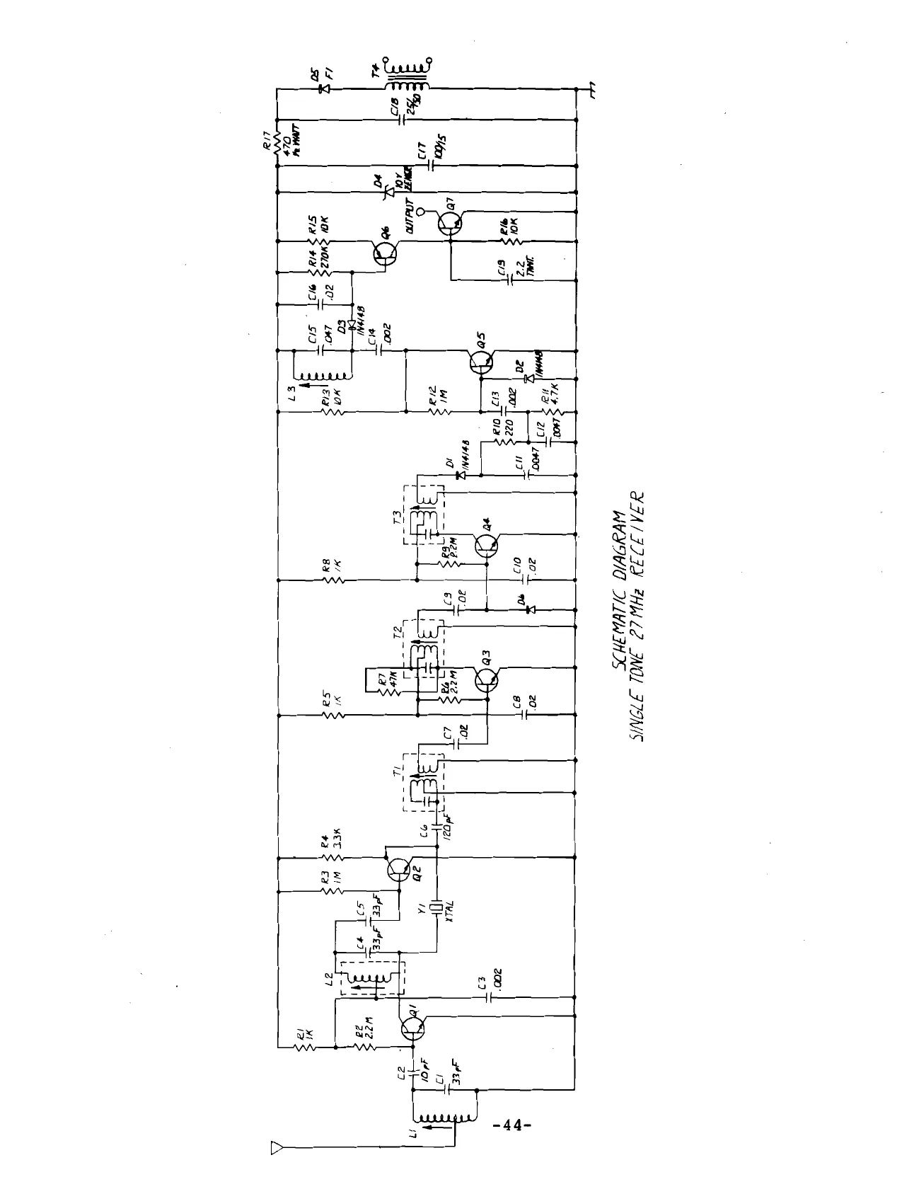
This page is a drawing, shown as the original scan.
This page reads as a drawing: its text was drawn rather than typeset, and comes out in fragments. See the original scan.
GREMLING
INDUSTRIES, INCORPORATED
crowp 7 MODEL 4001A
NOISE o LAMP BOARD & FRAME SCHEMATIC
CONN. “2 A ~ [ : if feccenee et ee FOUL| HOME TRI vi) ous a | *@ ae ZDIN BOX & CONNECTOR (- ---- $ L | if ; L... 7 awit Fay . t ala z IN 7 _— 7 —+ + Dee | 8 M4 <i T T id ral p22 n4 E @ CIO Q4) 6) ) 3) G42) G8) G3) At 14) 05) 06 ! 1 VOLOME R © i sure. } F 5 2? Z PYRE EEEY EEE EE SY ZeyyyyyyY ae OER suPR) U S | | =H | SPEAKER eS || fp ee is L & gt | MAuoR Y & = = NS ened $ ; a Dae 3 3 Cane ene 5. lie lent 5: ire ena TLS N — GAMES] TO YPLay [counT] it TF ——————— SICH N saul a 4 a {tf — MAJOR 1 a Eine | == mn My O ie reat I4VAes 16a — = Ht ! 1 T r 15 W 7 waar STR E tar TH 44 9 | | BALL "Oo Ltt i — rt rH a TI 044 onoe44 t+ _ Le TT I SCORE DISPLAY 4 E +t [ ie) 3 | Dts El tit | L| Ne j ® : ® © | tb K+}! $ _sin of mca 4 ad sens! @® itt diminarion: | ® UNITS | UNITS lo) T : 2 Wairs ACS Tae Ltd tu 7 t-a@ © | L ie 3
2 mi — +4 + : -|-|-|-] - -—- - --[-]-|-|-] o- TTT | t WOOO fal | || | hile aneazin ©] ‘@ (ne FU nelle LU SLIM oe SOX alele ues Pees SOLE x S%G PUR POPP PARLOLM XS
ee LOGIC BOARD CONNECTOR Bod
08 P13 C7 22/35 bt ae Bly
Pa
T t QUMCR (06-1 Q2 2N45060 Pa Q3 2N5060 i tJ I i C2 | E52 Re 3203 e7> 8. ~ 64] RIS Pid 65 | Re kee & 02 | 68 CBO. 02 680 2 485 Ge 280 2 OBO 02 680 o80¢ [2 {— {> a5 CB ns
R32 okt G50 80 t+ D4 BOs l RLS Bor D2 bdl2
R312.2M BA USED ONLY IN OPTION G. OMITTED IN STANDARD CANE. sen maTC poke % ALL TRANSISTORS @NEZEZA OR 2N4401. } , 3 ALL DIODES IN4ODE. POWER SUPPLY / SOUND GENERATION
2 ALL RESISTOR VALUES IN OHMS, Yo WATT. | ALL CAPACITOR VALLES IN MICROFARADS. GREMLIN INDUSTRIES, INC. D30 COWKOY CT, SAN DIEGO, CA, 92M!
NOTES: (UNLESS OTHERWISE SPECIFIED)
Reference Desig.
U-9,11,15,17,19,20,24 25,32,51 U-22,39,40,42,49,50 U-10,16, 21,37 u-48 U-27, 28,30 U-43,44,45,46 U-5,6,8,18,52 U-33,34,35,36 U-1,2,3,4,23 U-7,13,14,53 u-41 U-12,29 U-26,31,38,47 Q-1 thru Q-62 & Q-67 SCR 1-5 & 7-9,Q-63, 64,65,66 SCR-6,10 D-1 thru D-10 c-13 c-4,6,8,9,10,11,12, 14,17,18,19,20,21, 22,23, 24,25, 26, 27,28,29 C-1
R-6,52,53,57 R-86 R-1l thru R-4 R-17-33,44-48, 59-63, 70-75, 78-85 R-8,12,35,43,56,45 R-5 R-7,9,10,13-16, 37,38, 40,41,42,49-51,54,55, 64-66,68,69,76,77 R-12 R-10 R-36 R-58 R-39,67 R-11,34 PARTS LIST
Logic Board Assembly
4001A-DLC
Description
I.c. 7400 " I.c. 7404 I.C. 7408 I.C. 7410 I.c. 7442 I.c. 7448 I.c. 7474 I.C. 7475 I.c. 7490 I.C. 7493 I.c. 74154 I.C. 74193 I.C. NE555 Transistor 2N2222A/2N4401 SCR 2N5060
SCR MCR-106-1 Diodes 1N4002 Cap. 250pfd @50v Cap. .05mfd @50V
Cap. .1l5mfd @50V Cap. Imfd @16V Cap. 4.7mfd @16V Cap. lOmfd 16V Cap. 22mfd @16V Cap. 100mfd @16V Res. 180 1/2W Res. 330 1/2W Res. 390 1/2W Res. 680 1/2W "
Res. 1K 1/2W Res. 4.7K 1/2W Res. 10K 1/2W "
Res. 27K 1/2W Res. 47K 1/2W Res. 56K 1/2W Res. 62K 1/2W Res. 390K 1/2W Pot. 100K Gremlin Part #
314-0009
314-0015 314-0012 314-0010 214-0011 314-0013 314-0006 314-0017 314-0003 314-0005 314-0008 314-0007 314-0001 482-0003/482-0014 482-0009 " 482-0012 481-0001 151-0004 151-0001 "
152-0011 150-0009 150-0007 150-0006 150-0011 150-0010 471-0181 471-0331 471-0391 471-0681 "
471-0102 471-0472 471-0103
471-0273 471-0473 563-0563 471-0623 471-0394 475-0006
Reference Desig. Description Gremlin Part #
| n/a | Pins .045 sq. 3/4 in. | 212-0002 |
| n/a | 4001L Logic PC Board | 170-0009 |
| n/a | Connector, 10 Pin | 212-0005 |
Reference Desig.
Ic-1 Q-1 Q-2,3,4,5 Q-6,8 thru 14 Q-7,15 D-1,4-8,10-12,14 D-2,3,13 D-9 c-1 C-2-6,8,11 c-19,21 c-16,20, C-9,24,25 c-10 c-12 c-13 c-15 C-17,C-18 c-7 C-14 & 23 R-1,38 R-3 thru 12,14 R-13,27,33,39 R-15 R-16,18,25,34,21, 22 R-30 R-31 R-20,24 R-17,19, 23 R- 26 R-32
Cc-22 PARTS LIST
Power/Sound Board
4001A-PS
Description
Ic LM380N SCR MCR-106-1 SCR 2N5060 Transistor 2N2222A/2N4401 Transistor 2N3565 Diode 1N4002 Diode MR501 Zener MZ500-22 Cap. 4700mfd @16V Cap. .02mfd @50V Cap. .05mfd @50V Cap. 4.7mfd @16V Cap. 100mfd @25v Cap. lmfd @16V Cap. 250pf @50V Cap. .003 @50 Cap. 820pf @100 Cap. 1800pf #100 Cap. 22mfd @35V Cap. .00lmfd @50V Resistor 27K 1/2W Resistor 680 1/2W Resistor 10K 1/2W Resistor 1K 1/2W Resistor 1M 1/2W Resistor 100K 1/2W Resistor 2.2M 1/2W Resistor 220K 1/2W Resistor 4.7K 1/2W Resistor 680K 1/2W Resistor 6.8K 1/2W 4001A-PS Ckt Board Connector, 10 Pin, Female Connector, 4 Pin, Male Cap. 4.7 MFD @ 50V Gremlin Part #
313-0006 482-0012 482-0009 482-0003/482-0014 482-0002 481-0001 481-0004 481-0005 150-0005 150-0006 151-0001 150-0007 150-0013 150-0008 151-0004 151-0009 152-0007 152-0008 150-0001 151-0008 471-0273 471-0681 471-0103 471-0102 471-0105 471-0104 471-0225 471-0224 471-0472 471-0684 471-0682 170-0008 212-0005 212-0008 150-0002
Reference Desig.
VRL Tl T2 D-44,D-45 D-1 thru D~43 44 each 124 each 168 each s-1
F-1
J-1
R-36 R-2 R-1 PARTS LIST
Lamp Board and Frame Assembly
Description
Voltage Regulator-LM340T5 Transformer 61122 A Transformer 61219 A Diode MR751 Diode 1N4002 Lamp #756 Lamp #1813 Socket, Lamp Switch, DPDT Fuseholder Fuse, 2A Line Cord Socket (4 Pin, Female, Coin Box) Conn. Term. (Male, 10 Pin) Potentiometer, 10K Resistor 120 OHM, 2W Resistor 10 OHM, 15W Speaker Latches, Frame Receiver Transmitter Hinges P.C. Board (Lamp Board) Coin Box Gremlin Part # 313-0003 560-0004 560-0005 481-0002 481-0001 390-0004 390-0005 390-0002 510-0004 514-0005 514-0006 600-0002 211--0003 212-0008 475-0007 472-0121 474-0010 130-0005 280-0015 190-0002 190-0001 280-0013 170-0007 220-0001
RECOMMENDED SPARE PARTS FOR PLAY (Up to ten units)
Integrated Circuit 7400
| » | " | 7404 |
| " | " | 7408 |
| = | " | 7410 |
| u | " | 7442 |
| " | « | 7448 |
| " | " | 7474 |
| " | " | 7475 |
| * | " | 7490 |
| : | " | 7493 |
| fi | : | 74154 |
| " | il | 74193 |
Transistor 2N2222A
SCR 2N5060
" MCR-106-1
Diode 1N4002
Lamps #756
: #1813
Logic Board 4001A-DLC
Power Supply Board 4001A-PS
Transmitter BALL
each
each
each
each
each
each
each
each
each
each
each
each
each
each
each
each
each
each
each
each
each
The following section describes the 4001B-PS Power Sound Board which has succeeded the 4001A-PS Power Sound Board and is used only in the Model 4001B PLAY BALL game.
The circuit description is referenced to drawing no. 801-0003.
POWER SOUND BOARD 4001B-PS
POWER CONTROL:
The Power Control Circuitry (Power Buss Switching) Q-13 through Q-16 operates identical to that described on page 30.
BAT SOUND:
The Bat Sound for the 4001B-PS is quite different from that of the 4001A-PS.
The "Hit" signal is sensed at Pin 2 of the board connector and applied through D8 and R27 to the base of Q-12. Q-12 inverts the incoming pulse and applies it to the base of Q-11 through differentiating capacitor C-18.
C-18 detects the leading edge and Q-11 amplifies and squares the resultant narrow pulse. The output at the collector of Q-11 (a positive pulse) is applied to a damped oscillator consisting of the following three stages of U-l. The pulse shocks the oscillator into a short burst of oscillation which has the frequency and wave-shape characteristics similar to that of a bat sound.
SUMMING AMPLIFER:
U-1 (Pins 12,13814) forms an amplifier which combines the bat sound and crowd noise inputs and conditions them to be fed to the volume control potentiometer.
CROWD NOISE:
The crowd noise circuitry operates in a manner similar to that described on pages 30 and 31.
AUDIO AMPLIFIER:
U-2 is a self-contained 5 watt audio amplifier which processes the sound signals from the volume control and routes them to the speakers.
ceawo souno [33
NOMENCLATURE
BUSS
RB 10K - 213. MLR 10-1 R49 DIO
POWER
1 ezol, O7Jy4002| 10K:
pal e2gim 23h rab es, Qi amKS IMS 43K:
PITCH BUSS SECOND HALF,
FURST WALE,
IN lea02| es) OW (80
AFAR, inPur m4002
mB [2d ecririco[e auteur a TO SV REO. seavno[a}———4 ror our [BI por ew. [4} ——1 GREMLIN INDUSTRIES, INC. 7030 CONVOY (T., SAN DIEGO CA 92114 POWER/ SOUND BOARD SCHEMATIC
2 ALL RESISTOR YALWES IN OHMS, HALE WATT, 5%. MODEL 40018-PS
- ALL CAPACITOR YALUES IN MICROFARADS. ANNE NOTES: GnlesS OTHERWISE SPECIFIED) 60 9005 DME