Liberator SP-209 1st Printing
Liberator (version 2) (Atari, 1982) · Schematic Package · 29 pages · 88 sections · original scan

Sheet 1A
Sheet 1B
Sheet 2A
Sheet 2B
Sheet 3A
Sheet 3B
Sheet 4A
Sheet 4B
Sheet 5A
Sheet 5B
Sheet 6A
Sheet 6B
Sheet 7A
Sheet 7B
Sheet 8A
Sheet 8B
Sheet 9A
Sheet 9B— 11B
Sheet 12A— 13B
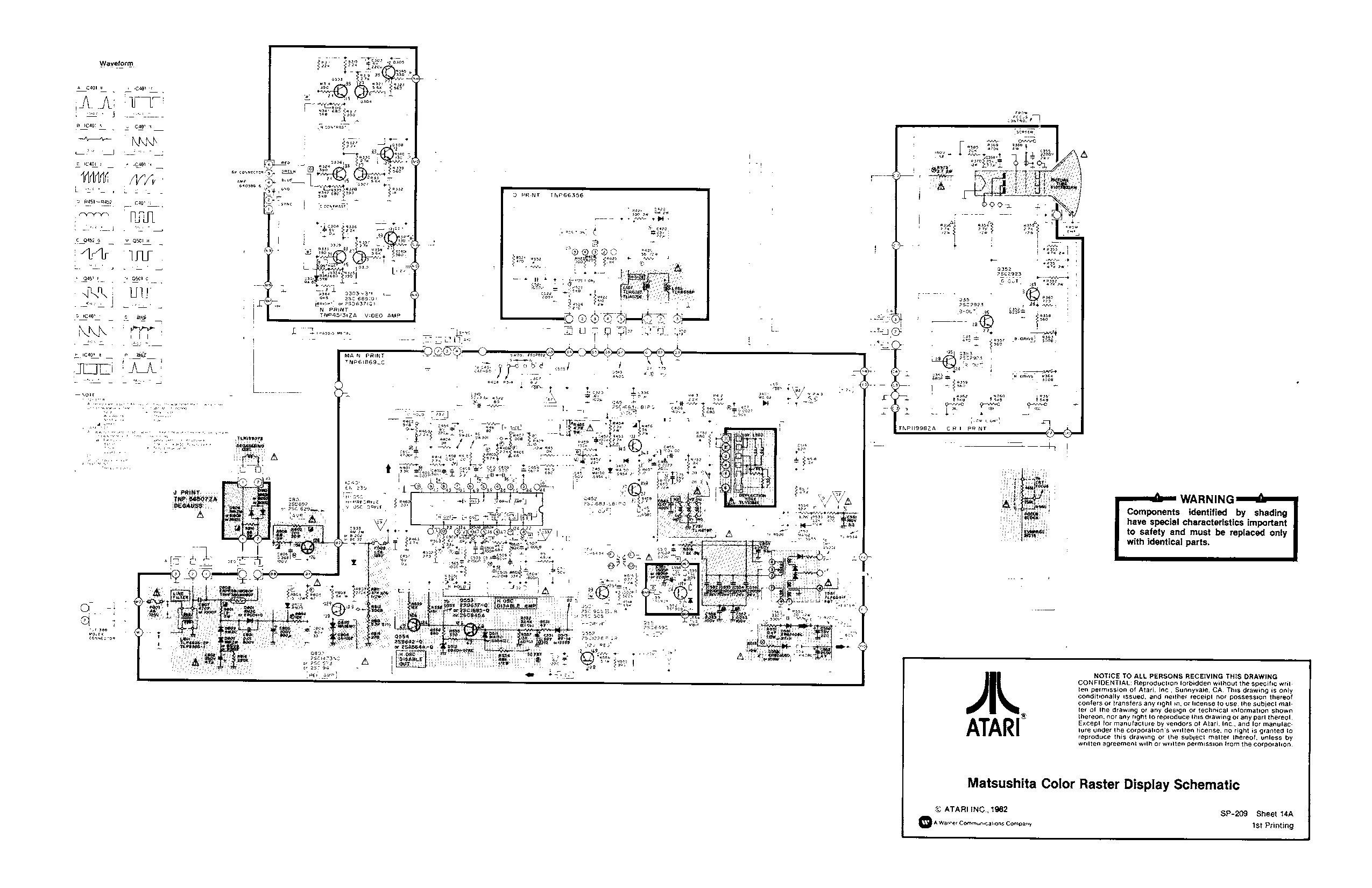
Sheet 14A
Sheet 14B
Sheet 15A Table of Contents
Table of Contents
Liberator Main Wiring Diagram (038726-01A)
Regulator/Audio Il PCB Schematic Diagram (A035435-02F), Color Raster Power Supply Wiring Diagram (037669-01C)
Coin-Door Wiring Diagram (A037542-01D), Utility Panel Wiring Diagram (A038004-01E), Fluorescent Light Wiring Diagram (035833-01A), Coupler PCB Schematic (A035220-02C)
Game PCB Schematics (038068-XXA), Sheets 3A—9A
Memory Map and Schematic Notes
Power Input, Clock, Power-On Reset, Watchdog
Test Connector, Microprocessor, Address Decoders
Program Memory, Bit Map Address Decoders, Write Protection, Refresh
EAROM and -28 Volt Supply
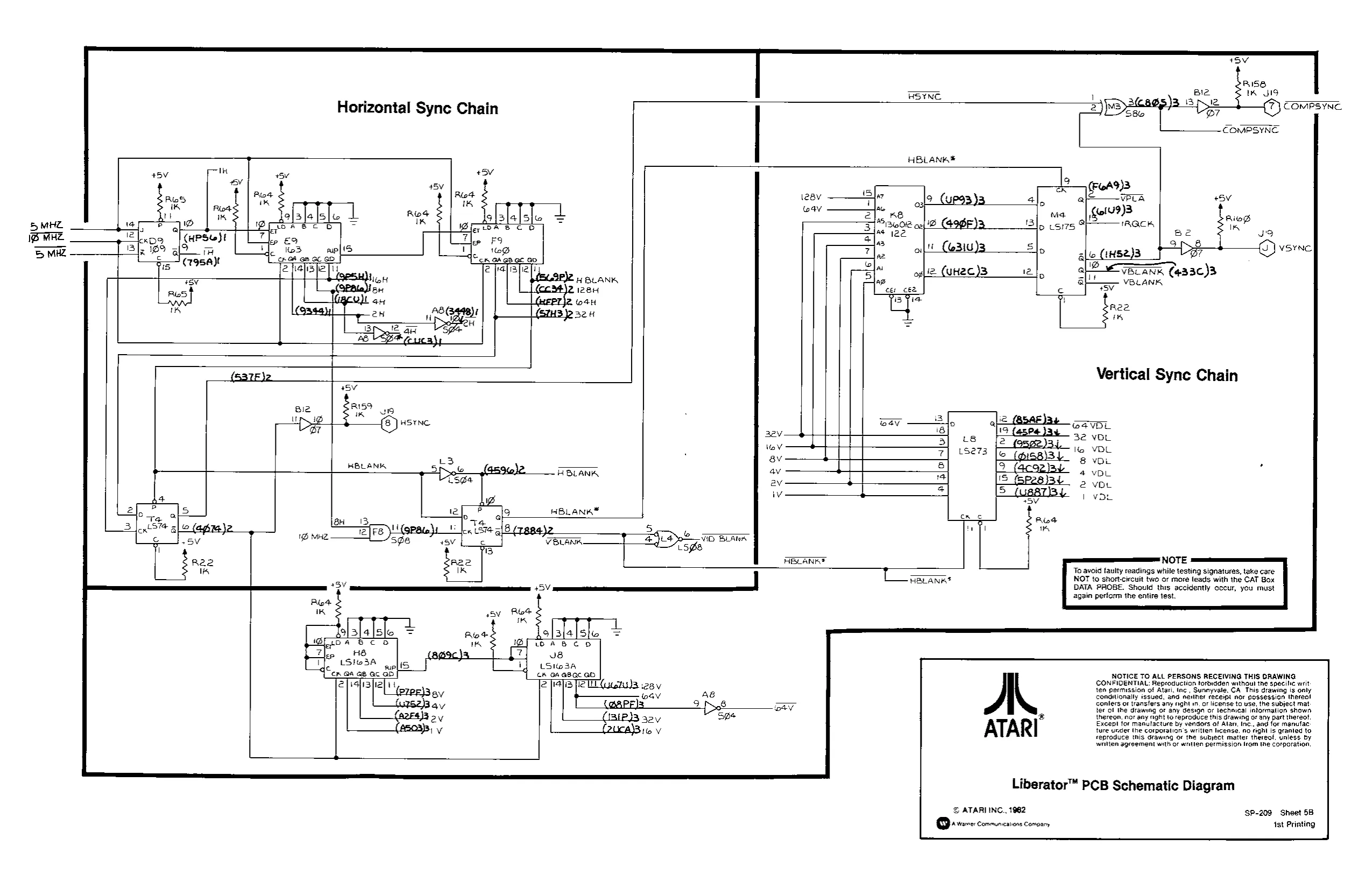
Vertical and Horizontal Sync Chains
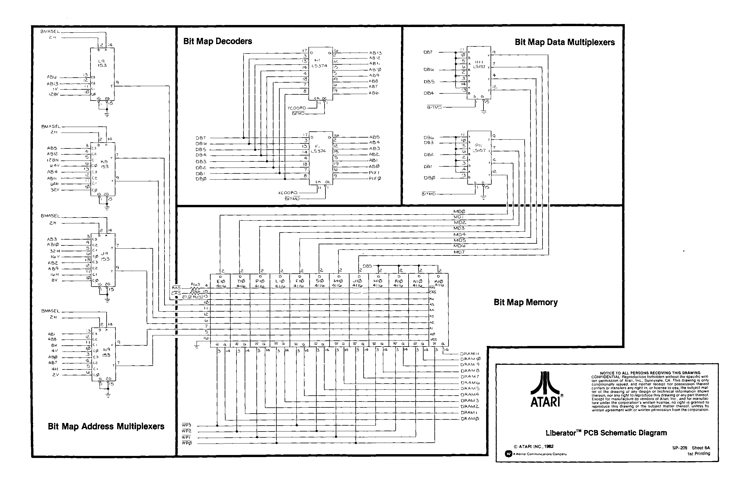
Bit Map Address Multiplexers, Bit Map Decoders, Bit Map Data Multiplexers, Bit Map Memory
Bit Map Data Buffers, Bit Map Shift Registers, Load Raster Control Latch, Planet Picture Memory, Planet Control, Planet ROM Address Generator
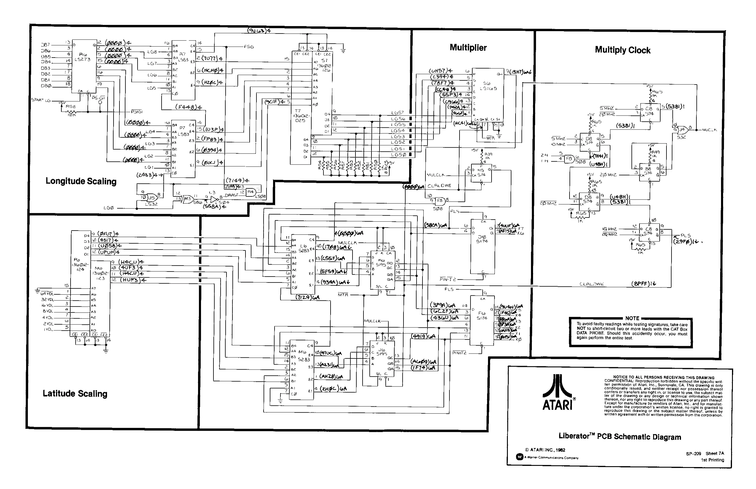
Longitude Scaling, Latitude Scaling, Multiply Clock, Multiplier
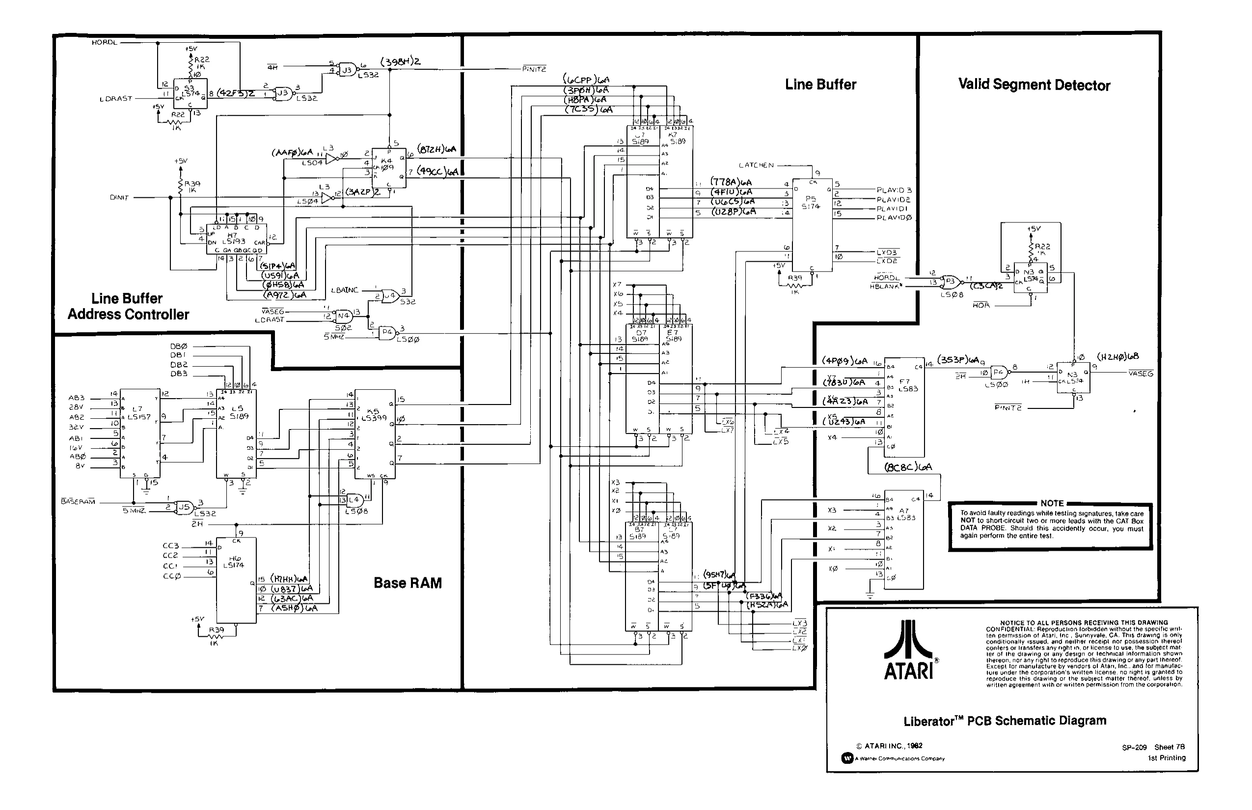
Line Buffer Address Controller, Base RAM, Line Buffer, Valid Segment Detector
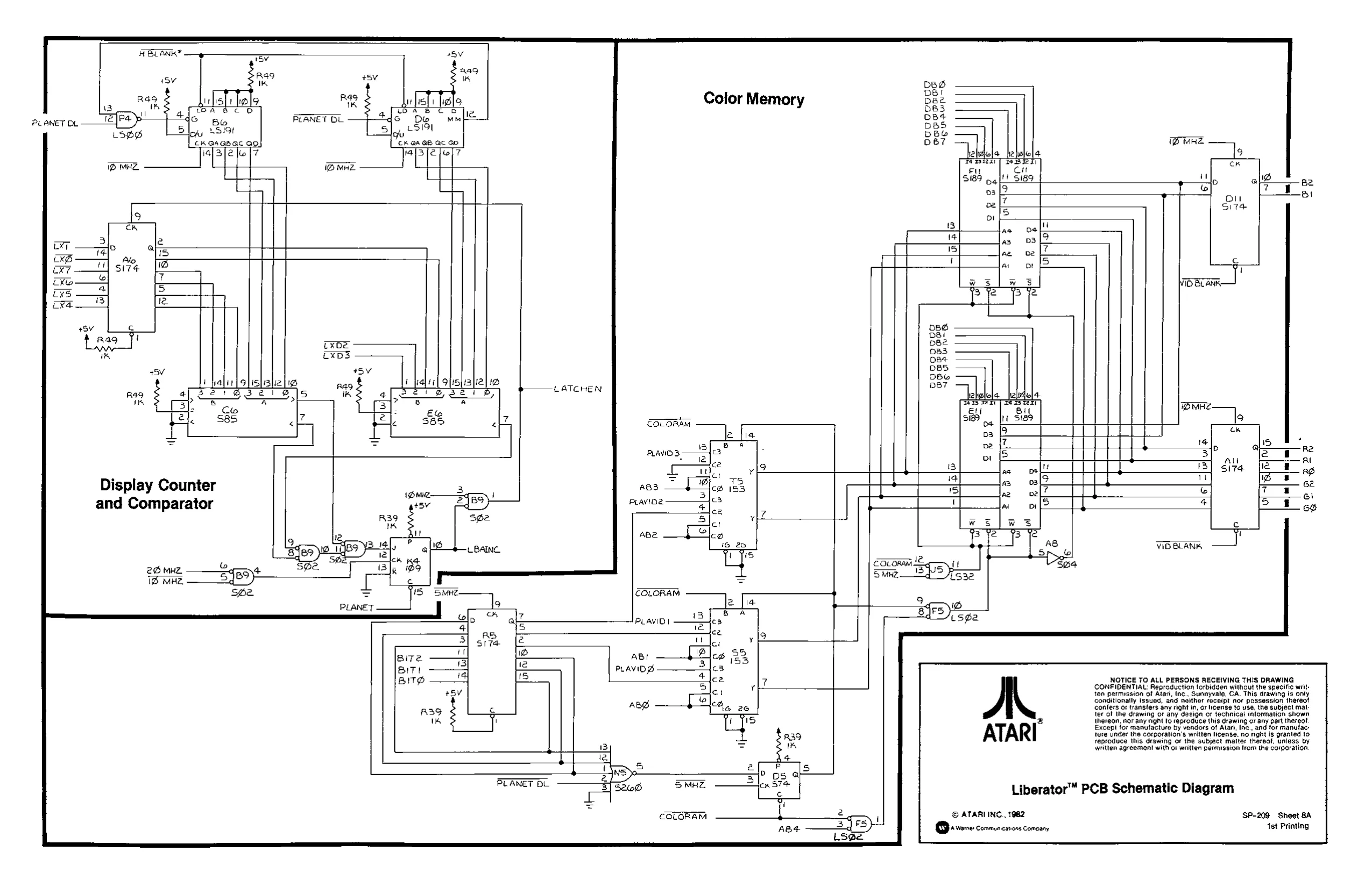
Display Counter and Comparator, Color Memory
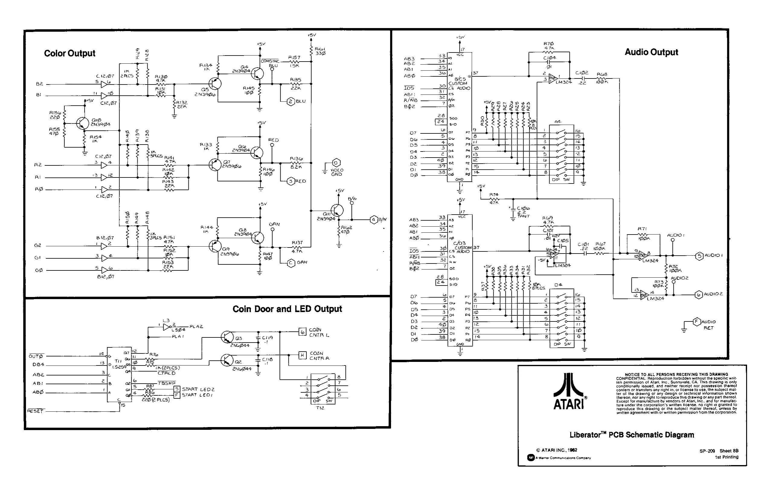
Color Output, Goin Counter and LED Output, Audio Output
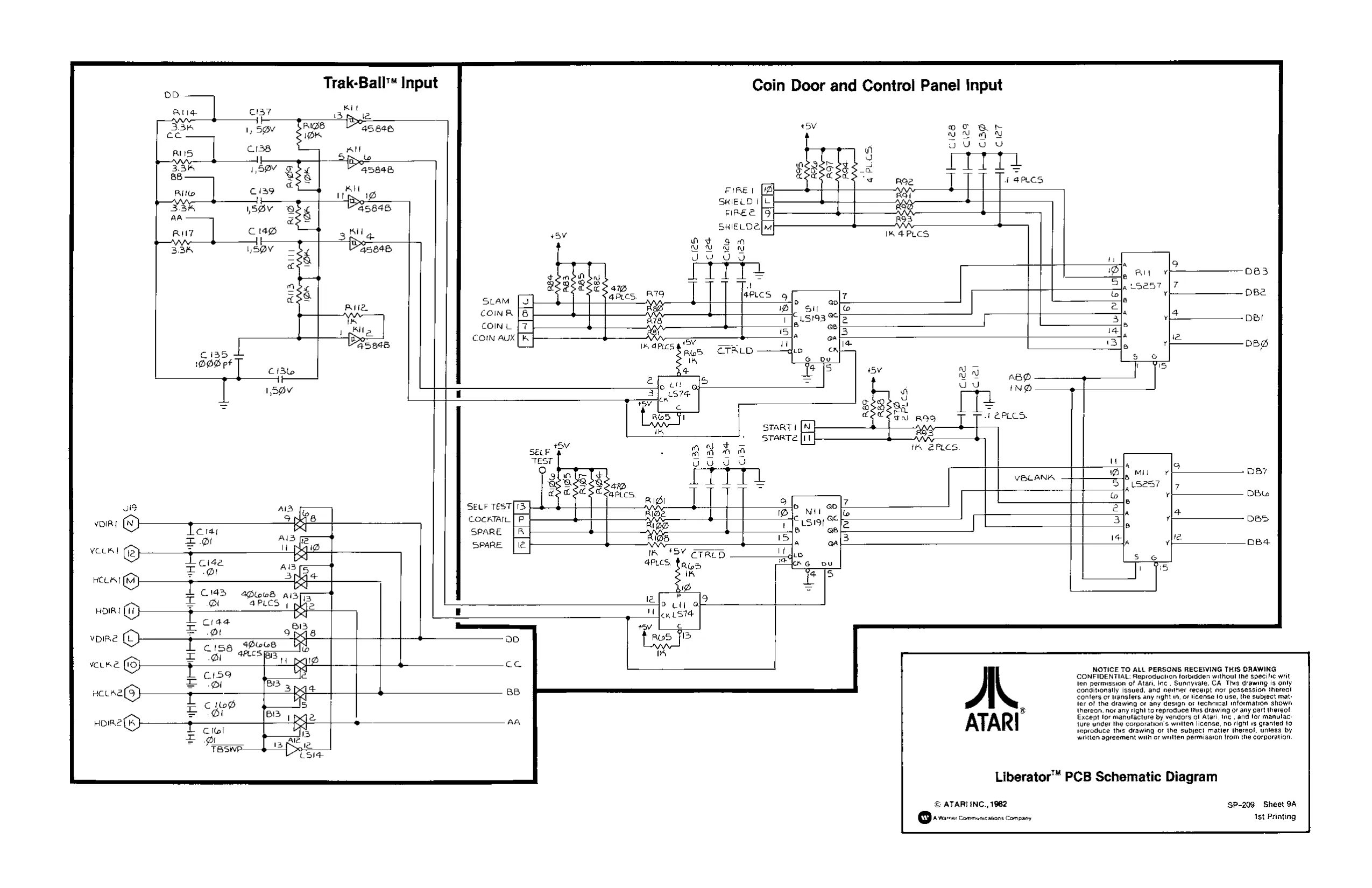
Trak-Ball™ Input, Coin Door and Control Panel Input
Liberator PCB Signal Name Descriptions
Liberator PCB Troubleshooting Procedures
Matsushita Color Raster Display Schematic (139003-1004)
Wells-Gardner Color Raster Display Schematic (92-055)
Electrohome Color Raster Display Schematic (92-049) © overe communes Conotny
schematics.
Schematic Package Supplement to
LIBERATOR
Operation, Maintenance, and Service Manual
40L
© ATARI, iNC., 1982
SP-209 Sheet 1A 1st Printing
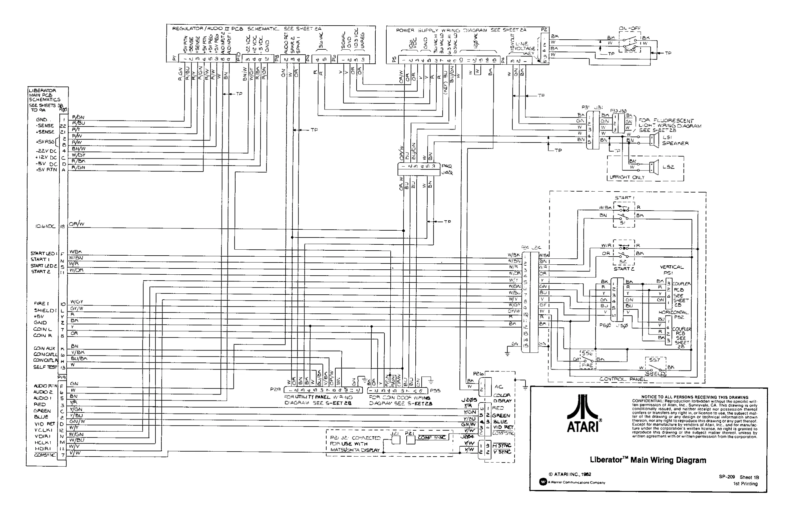
This page is a drawing, shown as the original scan.
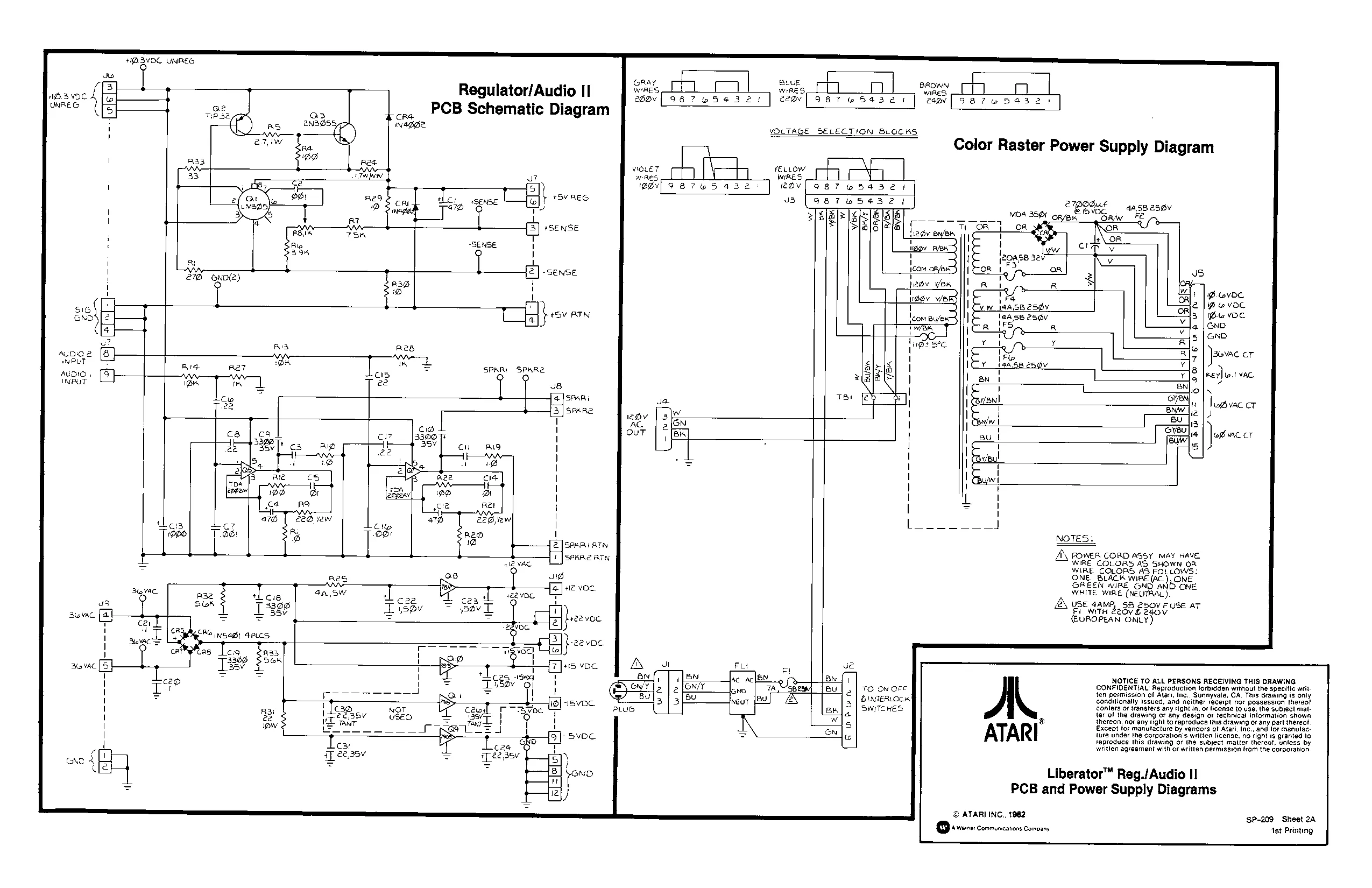
HB3VDC UNREG
Blue Regulator/Audio II ! oe 987 wS43e7 987? w5432)
— PCB Schematic Diagram
CRe nage VOLTAGE SELECTION BLOCKS
Color Raster Power Supply Diagram
YELLOW WIRES 12Ov . , cal de, *SENSE om ennee va 27POGat 48,58 250v Cs ae ae i MOA 3561 ones 2 OS, Ed
“SENSE
27 Gnol2) rom a x] } Y Lady yen i bev vie B-wvOr WP &vor IP VOC. GNoO GNO sv RIN
owe cr
key] o.1 VAC. § SON6 UREN
N lroghvac cr
\« vac CT
mane + 1D or ict Ro Ret a7 [ c2d yew ‘ 226, few] R: 7 R20 NOTES: 10 SPAR ATIN AS power SPKRERTN AN POWER CORD ASSY_MAY HAVE WIRE COLORS AS SHOWN OR WIRE COLORS AS FOLLOWS: ONE BLACK Wine (AC), ONE
- GREEN WIRE GND AND ONE. #2 vO. WHITE. WIRE (NEUTRAL). R32 tLe USE 4AMP, 58 250V FUSE AT SOK 3300 ; ° é Fi with deve sao” f 35Vv *22V00. (EUROPEAN ONY)
eave, Fo insast apices I Cas. Te a T3308 +15 VDC.
SWiTHES coniers or translers any right in, or license to use, the subject mat- NOTICE TO ALL PERSONS RECEIVING THIS DRAWING FO ONOFE CONFIDENTIAL: Reproduction forbidden without the specific writ ten permission of Atan., Inc.. Sunnyvale, CA. This drawing is only GINTERLOCK| conditionally issued, and neither receipt nor possession thereo!
ter of the drawing or any design or technical iniormation shown B thereon, nor any righ! to reproduce this drawing of any part thereot. Except for manutacture by vendors of Atari. (nc., and lor manulac: ture under the corgoration’s written license. no right 1s granted to Feproduce this drawing or (he subject matier thereof, unless by writlen agreement with or writlen permission from the corporation (Buson -)& WE ag Cag iy 22,35 aT eé ev Liberator™ Reg./Audio II
PCB and Power Supply Diagrams
© ATARIING., 1982 SP-209 Sheet 2A QQ Here: communcations Company Ast Printing
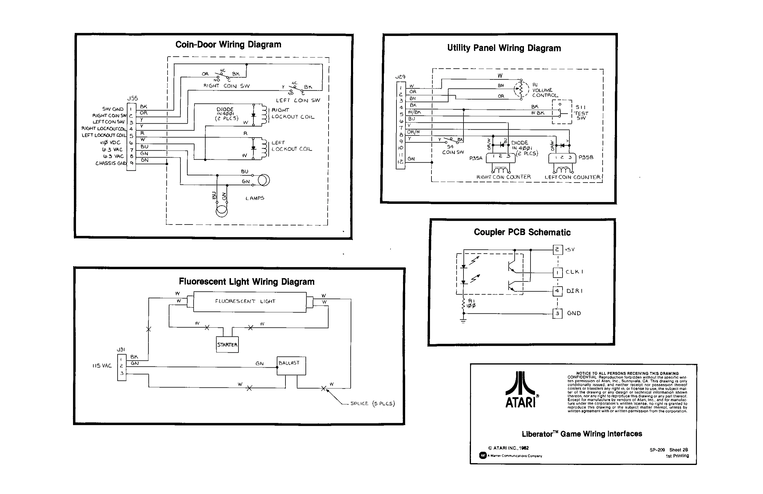
a re ra
SW GND
Coin-Door Wiring Diagram
RIGHT COIN SW] NC. RIGHT COIN SW Y Bn ot
LEFT COIN SW. RIGHT LOCKOUTCO LEFT LocKour coi] 41 VOC .3 VAC 3 VAC CHASSIS GNO gSeneusun—
J3!
i USVAC Ja LEFT COIN SW
DIODE RIGHT
(2 es) LOCKOUT COIL
w
Leer LOCKOUT COIL
Fluorescent Light Wiring Diagram
Ww
Ww FLUORESCENT LIGHT
GN BALLAST
| e x N\ SPLICE (5 PLCS)
Utility Panel Wiring Diagram
SerAg UAW RL } VOLUME. CONTROL,
RIGHT COIN COUNTER LEFT COIN COUNTER |
NOTICE TO ALL PERSONS RECEIVING THIS DRAWING CONFIDENTIAL: Reproduction forbidden without the specific wrt ten permission o Alaei, Inc., Sunnyvale. CA. This drawing is only conditionally issued, and neither receipt nor possession thereat conlers oF transiers any right 1n, or license to use, the subject mal ter of the drawing or any design or technical information shown ® thereon, nor any fight to reproduce this drawing or any part thereof, Except for manutacture by vendors of Atari, (nc., and for manufac: ture under Ine corporation's written license, no right 15 granted to reproduce this drawing or the subject matter thereo!, unless by written agreement with or written permission trom the corporation,
Liberator™ Game Wiring Interfaces
© ATARIING., 1962 $P-208 Sheet 28
|A Warmer Communcations Company ‘4st Printing
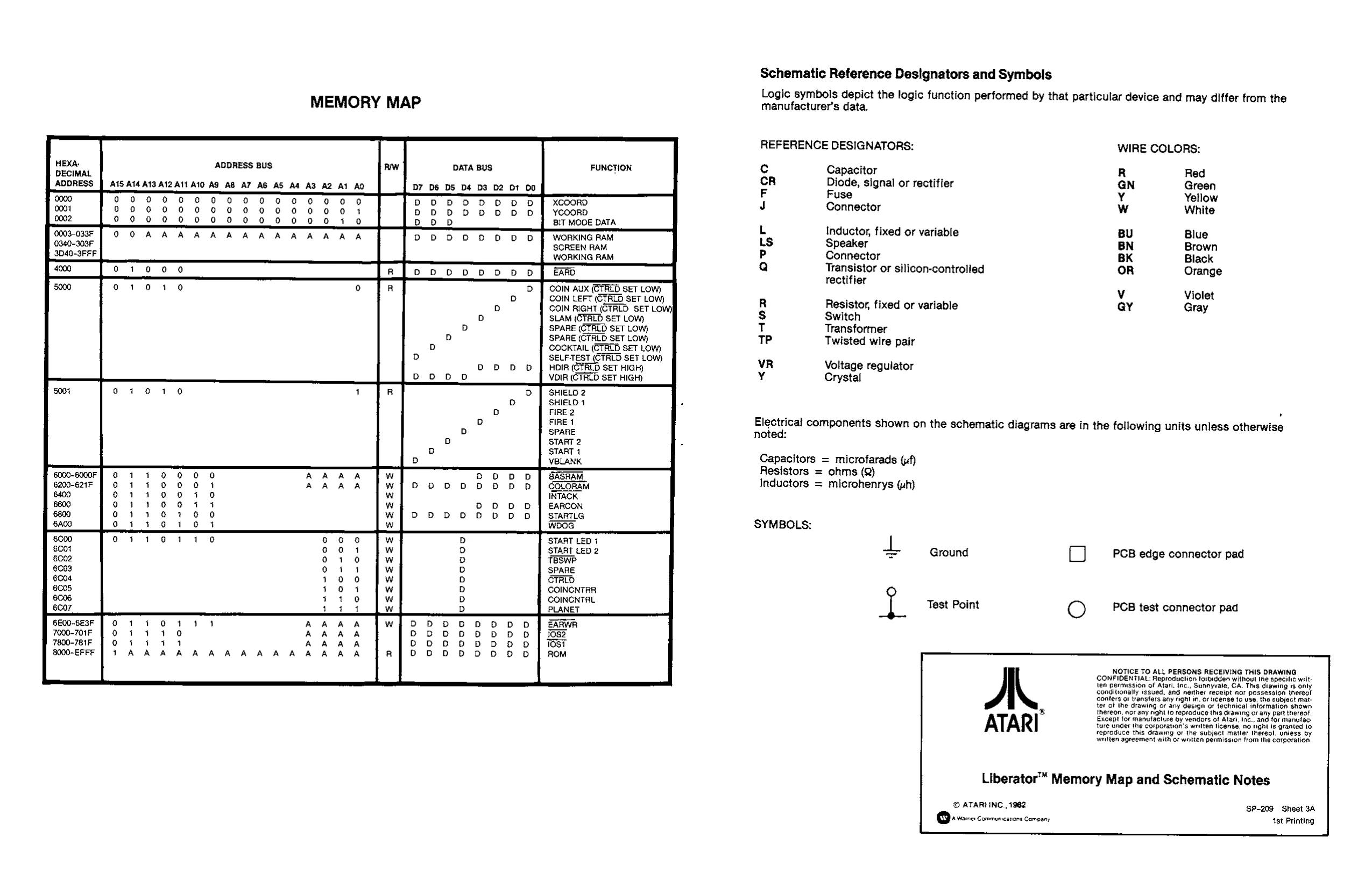
Schematic Reference Designators and Symbols
Logic symbols depict the logic function performed by that particular device and may differ from the MEMORY MAP manufacturer's data.
REFERENCE DESIGNATORS: WIRE COLORS:
bad aL ADDRESS BUS DATA BUS FUNCTION c Capacitor R Red
| ADDRESS | AIS A14 A13 A12 All A10 AS AB A7 AS AS A4 A3 A2 Al AO | D7 D6 DS Dé D3 D2 Dt DO | e | Paoe, sional or rectifier | Yn | vollow |
| 900000060000000000 | XCOORD | J | ij | |||
| 0 | 0 | oo | 00000010 | BIT MODE DATA | . | . |
| L | Inductor, fixed or variable | BU | Blue |
0 0 AAAAKRAAAAKA D2 © D D Ff WORKING RAM ts Speaker BN Brown
REEN RAM
WORKING RAM P Connector BK Black
Q Transistor or silicon-controlied OR Orange
rectifier
| COIN AUX (CTRLD SET LOW) | Vv | Violet | |
| COIN LEFT (CTRLD SET LOW) | n | + | 4 |
COIN RIGHT (CTRLD SET Low] § Resistor, fixed or variable GY Gray
SLAM (CTRLD SET LOW Switch
| SPARE (CTRLD SET LOW) | T | Transformer |
| SPARE (CTRLD SET LOW) | TP | Twisted wire pair |
COCKTAIL (CTRUD SET LOW) SELF-TEST (CTRLD SET LOW}
| HDIR (GTRLD SET HIGH) | VR | Voltage regulator |
| VDIR (GTRLD SET HIGH) | Y | Crystal |
6200-621F
6E00-6E3F 7000-701F 7800-781F 8000-EF FF D bo} D
o D D D
o o o o SHIELD 2 SHIELD 1 FIRE 2 FIRE 1 SPARE START 2 START 1 VBLANK
START LED 1 START LED 2 TBSWwP SPARE GTRLO COINCNTRR COINCNTRL Blegtical components shown on the schematic diagrams are in the following units unless otherwise noted:
Capacitors = microfarads (uf) Resistors = ohms (Q) Inductors = microhenrys (uh)
SYMBOLS: ae Ground OJ
Test Point PCB edge connector pad
O PCB test connector pad
CONFIDENTIAL: Reproduciion forbidden without the spe NOTICE TO ALL PERSONS RECEIVING THIS DRAWING w w w w w w
w w w w w w w w
ten permussion of Atari, inc., Sunnyvale, CA. This drawing is only conditionally issued. and neither receipt nor possession thereol in. OF liCense to use, the subject matjesign or technical information shown thereon. nor any right to reproduce this drawing or any part thereof, Except for manufacture by vendors of Alar), Inc., and for manufac: ture under Ihe corporation's wrilten license, no night is granted to feproduce this drawing of the subject matier thereol, unless by wniten agreement with of waiten permission from the corporation A ATARI
Liberator™ Memory Map and Schematic Notes
© ATAR?NC., 1962 Or vere conmenciens Cnoeny SP-209 Sheet 3A
1st Printing
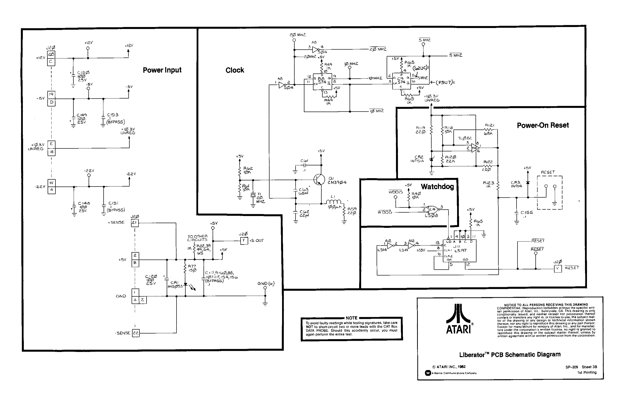
Power Input
JO OTHER CIRCUITS
Re2,39 1h 3 49,64, 5Y we | 4
RIT BD la1.7.5-1095,88, 1B7-I 1,154, (Sto (errAss)
Power-On Reset
ATARI
NOTICE TO ALL PERSONS RECEIVING THIS DRAWING CONFIDENTIAL: Reproduction forbidden without the specilic written permission of Atarl, Inc , Sunnyvale, CA. This drawing is only conditionally issued, and neither receipt nor possession thereof confers or (ranslers any right tn, oF license to use, ihe subject mat ter of the drawing or any design of technical inlormation shown thereon, nor any right to reproduce this drawing of any part thereot, Except far manufacture by vendors of Atari, Inc., and for manufac: ture under the corporation's watten license, no right is granted to reproduce this drawing of the subject matter thereof, unless by writien agreement with or walten permission trom the corporation,
Liberator™ PCB Schematic Diagram
© ATARIINC.,1982 SP-208 Sheet 3B 4st Printing
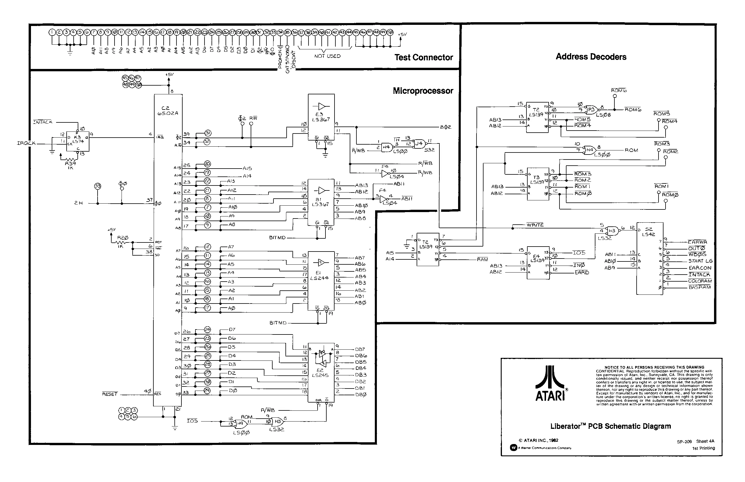
This page is a drawing, shown as the original scan.
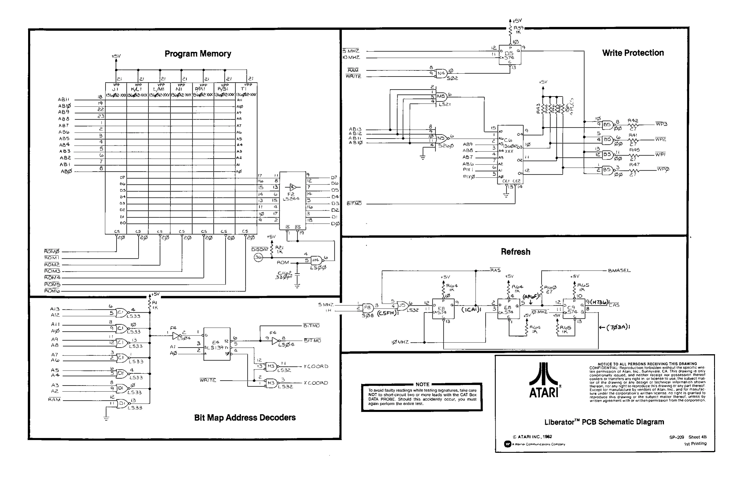
This page is a drawing, shown as the original scan.
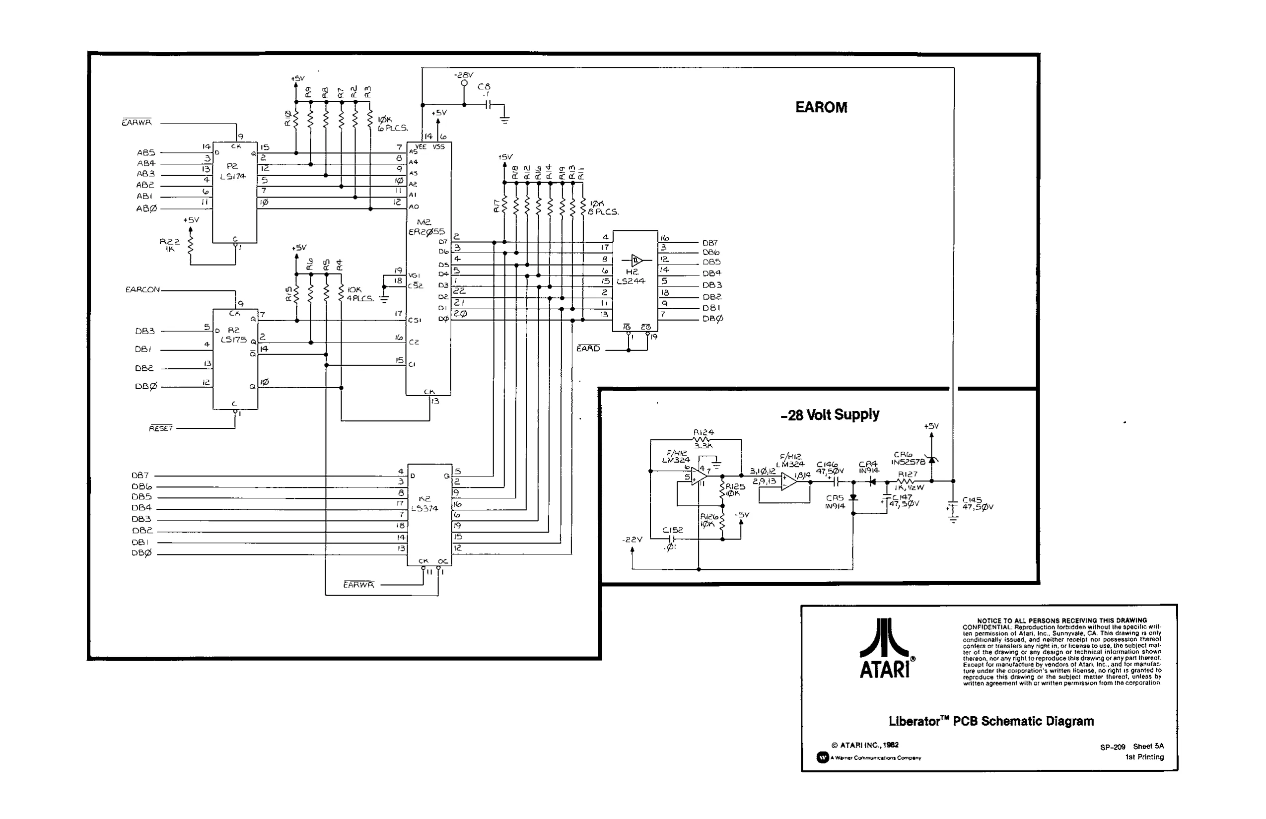
This page is a drawing, shown as the original scan.
This page is a drawing, shown as the original scan.
This page is a drawing, shown as the original scan.
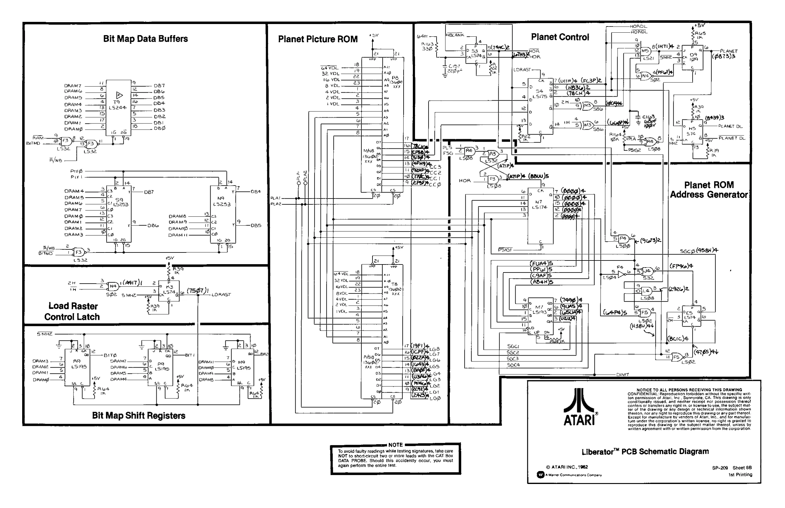
Bit Map Data Buffers
2H
Load Raster Control Latch
=f) UATE 2 iw ——+4 3 SO2 SMHZ—pay— Rw
Bit Map Shift Registers
Planet Picture ROM
teat BLANIS Planet Control = im
BDL
2v0u VOL EP
ig) 44, supe eres a
rc
aa
a
ne
a ao a|. * q2douse (rc3Pye tI} Sle z 2, ae ecn
an. 6 jo) Peas
aU D a KS edo ‘S86
Planet ROM Address Generator
aon
e+ VOL
32 VDL. Novo
ByOL: avon. 2vOL
1vou, ol aje{ujalul[nt-|s]a)ala
To avoid faulty readings while testing signatures, take care NOT to short-circuit two or more leads with the CAT Box DATA PROBE. Should this accidently occur, you must again perform the entire test. NOTICE TO ALL PERSONS RECEIVING THIS DRAWING CONFIDENTIAL: Reproduction forbidden without the specitic writ. en permission of Atari, inc, Sunnyvale, CA. This drawing is only conditionally issued, and neither receipt nor possession thereot conters or Iransters any right in, oF license fo use, the subject matler of the drawing or any design oF lechnical information shown Ihereon, nor any right to reproduce this drawing or any part thereol, Except for manulacture by vendors of Atari. nc., and for manutac: ture under the corporation's written license, no Fight 18 granted (0 reproduce this drawing or the subject matier thereof. unless by written agreement with or written permission trom the corporation. A
ATARI
Liberator™ PCB Schematic Diagram
© ATARI INC., 1982 (Qo vore:conmencasorsconpary SP-209 Sheet 68 Yt Printing
This page is a drawing, shown as the original scan.
This page is a drawing, shown as the original scan.
This page is a drawing, shown as the original scan.
This page is a drawing, shown as the original scan.
This page is a drawing, shown as the original scan.
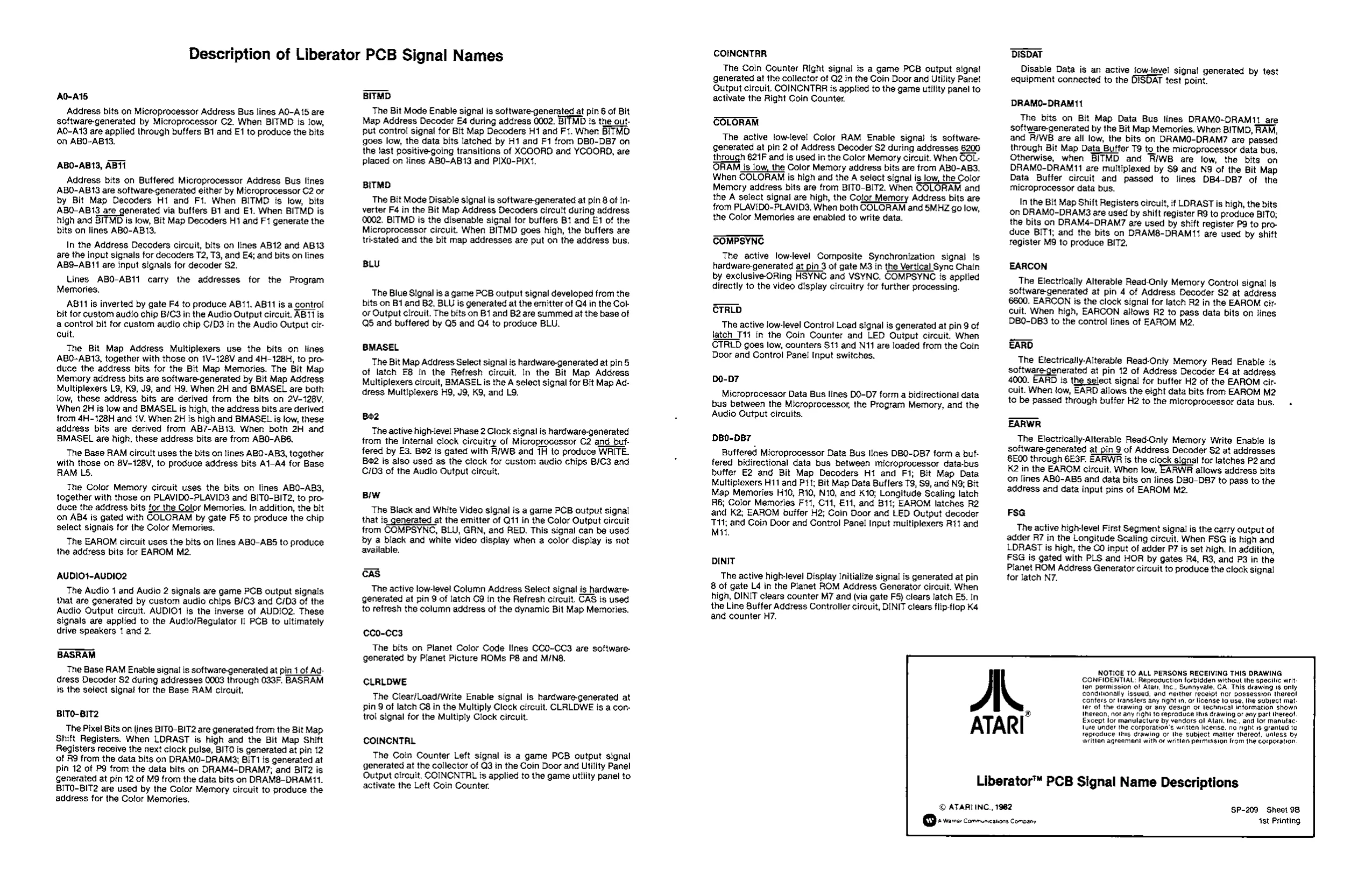
Description of Liberator PCB Signal Names
A0-A15
Address bits on Microprocessor Address Bus lines AO-A15 are software-generated by Microprocessor C2. When BITMD is low, A0-A13 are applied through buffers B1 and E1 to produce the bits on ABO-ABI3.
ABO-AB13, ABI1 Address bits on Buffered Microprocessor Address Bus lines ABO-AB13 are software-generated either by Microprocessor C2 or by Bit Map Decoders H1 and F1. When BITMD is low, bits ABO-AB13 are generated via buffers B1 and Et. When BITMD is high and BITMD is low, Bit Map Decoders H1 and F1 generate the bits on lines ABO-AB13, In the Address Decoders circuit, bits on lines AB12 and AB13 are the input signals for decoders T2, T3, and E4; and bits on lines AB9-AB11 are input signals for decoder $2. Lines ABO-AB11 carry the addresses for the Program Memories. AB11 is inverted by gate F4 to produce AB11, AB11 is a contro! bit for custom audio chip B/C3 in the Audio Output circuit. ABT is a control bit for custom audio chip C/D3 in the Audio Output circuit. The Bit Map Address Multiplexers use the bits on lines ABO-AB13, together with those on 1V-128V and 4H-128H, to produce the address bits for the Bit Map Memories. The Bit Map Memory address bits are software-generated by Bit Map Address Multiplexers LS, K9, J9, and H9. When 2H and BMASEL are both low, these address bits are derived from the bits on 2V-128V. When 2H is low and BMASEL is high, the address bits are derived from 4H-128H and 1V. When 2H is high and BMASEL is low, these address bits are derived from AB7-AB13. When both 2H and BMASEL are high, these address bits are from ABO-AB6. The Base RAM circuit uses the bits on lines ABO-AB3, together with those on 8V-128V, to produce address bits A1-A4 for Base RAM LS. The Color Memory circuit uses the bits on lines ABO-AB3, together with those on PLAVIDO-PLAVID3 and BITO-BIT2, to produce the address bits for the Color Memories. In addition, the bit on ABS is gated with COLORAM by gate F5 to produce the chip select signals for the Color Memories. The EAROM circuit uses the bits on lines ABO-ABS to produce the address bits for EAROM M2.
AUDIO1-AUDIO2 The Audio 1 and Audio 2 signals are game PCB output signals that are generated by custom audio chips B/C3 and C/D3 of the Audio Output circuit. AUDIO1 is the inverse of AUDIO2. These signals are applied to the Audio/Regulator Ii PCB to ultimately drive speakers 1 and 2.
BASRAM The Base RAM Enable signal is software-generated at pin 1 of Address Decoder S2 during addresses 0003 through 033F. BASRAM is the select signal for the Base RAM circuit.
BITO-BIT2 The Pixel Bits on lines BITO-BIT2 are generated from the Bit Map. Shift Registers. When LORAST is high and the Bit Map Shift Registers receive the next ciock pulse, BITO is generated at pin 12 of RQ from the data bits on DRAMO-DRAM3; BIT1 is generated at pin 12 of PQ from the data bits on DRAM4-DRAWM7; and BIT2 is generated at pin 12 of M9 from the data bits on DRAM8-DRAM11. BITO-BIT2 are used by the Color Memory circuit to produce the address for the Color Memories. BITMD
The Bit Mode Enable signal is software-generated at pin 6 of Bit Map Address Decoder E4 during address 0002. BITMD is the output control signat for Bit Map Decoders H1 and F1. When BITMD goes low, the data bits latched by H1 and F1 from DBO-DB7 on the fast positive-going transitions of XCOORD and YCOORD, are placed on lines ABO-AB13 and PIXO-PIX1.
BITMD The Bit Mode Disable signal is software-generated at pin 8 of inverter F4 in the Bit Map Address Decoders circuit during address. 0002. BITMD is the disenable signal for buffers B1 and E1 of the Microprocessor circuit. When BITMD goes high, the buffers are tri-stated and the bit map addresses are put on the address bus.
BLU
The Blue Signal is a game PCB output signal developed from the bits on B1 and B2. BLU is generated at the emitter of Q4 in the Col or Output circuit. The bits on Bt and B2 are summed at the base of QS and buffered by Q5 and O4 to produce BLU.
BMASEL The Bit Map Address Select signal is hardware-generated at pin 5 of latch E8 in the Refresh circuit. In the Bit Map Address Multiplexers circuit, BMASEL is the A select signal for Bit Map Address Multiplexers H9, J9, K9, and L9.
Bo2
The active high-level Phase 2 Clock signal is hardware-generated
from the internal clock circuitry of Microprocessor C2 and_buffered by E3. BO2 is gated with R/WB and 1H to produce WAITE. Bo2 is also used as the clock for custom audio chips B/C3 and CIDS of the Audio Output circuit.
Biw
The Biack and White Video signal is a game PCB output signal that is generated at the emitter of Q11 in the Color Output circuit trom COMPSYNC, BLU, GRN, and RED. This signal can be used by a black and white video display when a color display is not available.
CAS The active low-level Column Address Select signal is hardwaregenerated at pin 9 of latch C9 in the Refresh circuit. CAS is used to refresh the column address of the dynamic Bit Map Memories.
CC0-CC3 The bits on Planet Color Code lines CCO-CC3 are softwaregenerated by Planet Picture ROMs P8 and M/N8.
CLRLDWE The Clear/Load/Write Enable signal is hardware-generated at pin 9 of latch C8 in the Multiply Clock circuit. CLRLDWE is a control signal for the Multiply Clock circuit.
COINCNTRL The Coin Counter Left signal is a game PCB output signal generated at the collector of Q3 in the Coin Door and Utility Panel Output circuit. COINCNTRL is applied to the game utility panel to activate the Left Coin Counter. COINCNTRR: The Coin Counter Right signal is a game PCB output signat generated at the collector of Q2 in the Coin Door and Utility Panet Output circuit. COINCNTAR is applied to the game utility panel to activate the Right Coin Counter.
COLORAM
The active low-level Color RAM Enable signal is software. generated at pin 2 of Address Decoder $2 during addresses 6200 through 621F and is used in the Color Memory circuit. When COL- ‘ORAM is low, the Color Memory address bits are from ABO-AB3. When COLORAN is high and the A select signal is low, the Color Memory address bits are from BITO-BIT2. When COLORAM and the A select signal are high, the Color Memory Address bits are from PLAVIDO-PLAVID3, When both COLORAM and 5MHZ go low, the Color Memories are enabled to write data.
COMPSYNC. The active low-level Composite Synchronization signal is
hardware-generated at pin 3 of gate M3 in ee Vertical Syne Chain
by exclusive-ORing HSYNC and VSYNC. COMPSYNC is applied directly to the video display circuitry for further processing.
CTRLD
The active low-level Control Load signal is generated at pin 9 of latch T11 in the Coin Counter and LED Output circuit. When CTRLD goes low, counters $11 and N11 are loaded from the Coin Door and Gontrol Panel Input switches.
DQ-D7 Microprocessor Data Bus lines D0-D7 form a bidirectional data bus between the Microprocessor, the Program Memory, and the Audio Output circuits.
DBO-DB7 Buffered Microprocessor Data Bus lines DBO-DB7 form a buffered bidirectional data bus between microprocessor data-bus buffer E2 and Bit Map Decoders H1 and F1; Bit Map Data Multiplexers H11 and Pt; Bit Map Data Buffers TS, S9, and NQ; Bit Map Memories H10, Ri0, N10, and K10; Longitude Scaling latch R6; Color Memories F11, C11, £11, and B11; EAROM latches R2 and K2, EAROM buffer H2; Coin Door and LED Output decoder T11; and Coin Door and Control Panel Input multiplexers R11 and Mit,
DINIT
The active high-level Display Initialize signal is generated at pin 8 of gate L4 in the Planet ROM Address Generator circuit. When. high, DINIT clears counter M7 and (via gate F5) clears latch E5. In the Line Buffer Address Controller circuit, DINIT clears flip-flop K4 and counter H7.
AL
ATARI
DISDAT Disable Data is an active jow-level signal generated by test equipment connected to the DISDAT test point.
DRAMO-DRAMI11 The bits on Bit Map Data Bus lines DRAMO-DRAM11 are software-generated by the Bit Map Memories. When BITMD, RAM, and RIWB are all low, the bits on DRAMO-DRAM?7 are passed through Bit Map Data Buffer TS to the microprocessor data bus. Otherwise, when BITMD and RWB are low, the bits on ORAMO-DRAM11 are multiplexed by S9 and N@ of the Bit Map Data Buffer circuit and passed to lines DB4-DB7 of the microprocessor data bus. In the Bit Map Shift Registers circuit, if LORAST is high, the bits on DRAMO-DRAN3 are used by shift register RS to produce BITO; the bits on DRAM4-DRAN7 are used by shift register P9 to produce BIT1; and the bits on DRAM8-DRAM11 are used by shift register M9 to produce BIT2,
EARCON The Electrically Alterable Read-Only Memory Control signal is software-generated at pin 4 of Address Decoder S2 at address 6600. EARCON is the clock signal for latch R2 in the EAROM circuit. When high, EARCON allows R2 to pass data bits on lines DBO-DB3 to the control lines of EAROM M2.
EARD The Etectrically-Alterable Read-Only Memory Read Enable is software-generated at pin 12 of Address Decoder E4 at address 4000. EARD is the select signal for buffer H2 of the EAROM circuit. When tow, EARD allows the eight data bits from EAROM M2 to be passed through buffer H2 to the microprocessor data bus. +
EARWR The Electrically-Alterable Read-Only Memory Write Enable is software-generated at pin 9 of Address Decoder S2 at addresses E00 through 6E3F. EARWR is the cigck signal for latches P2 and 2 in the EAROM circuit. When low, EARWR allows address bits ‘on lines ABO-ABS and data bits on lines DBO-D87 to pass to the address and data input pins of EAROM M2.
FSG The active high-evel First Segment signal is the carry output of adder R7 in the Longitude Scaling circuit. When FSG is high and LDRAST is high, the CO input of adder P7 is set high. In addition, FSG is gated with PLS and HOR by gates R4, R3, and P3 in the Planet ROM Address Generator circuit to produce the clock signal for latch N7.
NOTICE TO ALL PERSONS RECEIVING THIS DRAWING CONFIDENTIAL: Reproduction forbidden without the specilic writ: ten permission of Atan, Inc., Sunnyvale, GA, This drawing 1s only congnonally issued, and neither receipt nor possession thereo! confers of ransters any right in, oF license to use. the subject mat ler of the drawing or any design of technical iniormation shown thereon, not any right to reproduce this drawing or any part thereot Except ior manulacture by vendors ol Atari Inc.. and tor manutac: lute under the corporation's written tcense. no right 16 granted to reproduce this drawing or the subject matter thereof, unless by writlen agreement with or writlen permission from the corporation
Liberator™ PCB Signal Name Descriptions
© ATARIINC., 1982 SP-209 Sheet 98 > tare Communcatons Company Ast Printing
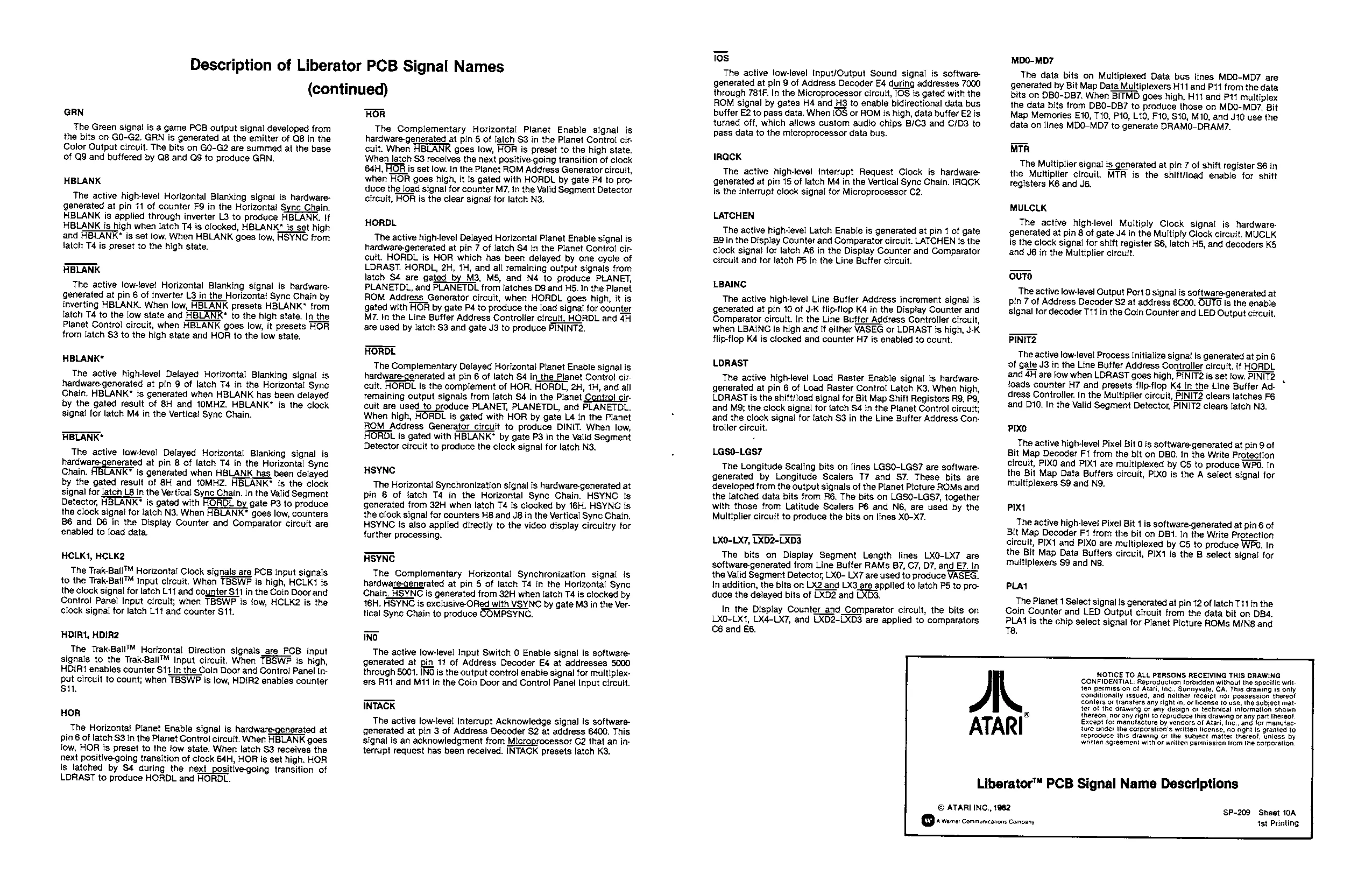
Description of Liberator PCB Signal Names
(continued)
GRN The Green signal is a game PCB output signal developed from the bits on GO-G2. GRN is generated at the emitter of Q8 in the Color Output circuit. The bits on GO-G2 are summed at the base of Q9 and buffered by Q8 and Q$ to produce GRAN.
HBLANK The active high-level Horizontal Blanking signal is hardwaregenerated at pin 11 of counter F9 in the Horizontal Syne Chain. HBLANK is applied through inverter L3 to produce HBLANK, If H@LANK is high when latch T4 is clocked, HBLANK" is set high and HBLANK’ is set low. When HBLANK goes low, HSYNC from fatch T4 is preset to the high state.
HBLANK The active low-level Horizontal Blanking signal is hardwaregenerated at pin 6 of inverter L3 in the Horizontal Sync Chain by inverting HBLANK. When low, HBLANK presets HBLANK* from latch T4 to the low state and HBLANK* to the high state. In the Planet Control circuit, when HBLANK goes low, it presets HOR from latch $3 to the high state and HOR to the low state.
HBLANK* The active high-level Delayed Horizontal Blanking signal is hardware-generated at pin 9 of latch T4 in the Horizontal Sync Chain. HBLANK" is generated when HBLANK has been delayed by the gated result of 8H and 10MHZ. HBLANK® is the clock signat for latch Md in the Vertica! Syne Chain.
HBLANK* The active low-level Delayed Horizontal Blanking signal is
hardware generated at pin 8 of latch T4 in the Horizontal Sync
Chain, NK® is generated when HBLANK has been delayed by the gated resuit of 8H and 10MHZ. HBLANK’ is the clock signal for latch L9 in the Vertical Syne Chain. In the Valid Segment Detector, HBLANK® is gated with HORDL by gate P3 to produce the clock signal for latch N3. When HBLANK* goes low, counters BS and D6 in the Display Counter and Comparator circuit are enabled to load data.
HCLK1, HCLK2 The Trak-Ball™ Horizontal Clock signals ate PCB input signals. to the Trak-Ball™ Input circuit. When TBSWP is high, HCLK1 is the clock signal for latch L11 and counter $11 in the Goin Door and Control Panel Input circuit; when TBSWP is fow, HCLK2 is the clock signal tor latch L11 and counter $11.
HDIR1, HDIR2 The Trak-Ball™ Horizontal Direction signals_are PCB input signals to the Trak-Ball™ Input circuit. When TBSWP is high, HDIRt enables counter S11 in the Coin Door and Contro! Panel Input circuit to count; when TBSWP is low, HDIR2 enables counter Sit.
HOR The Horizontat Planet Enable signal is hardware-generated at pin 6 of latch $3 in the Planet Control circuit. When HBLANK goes Jow, HOR is preset to the low state. When latch $3 receives the next positive-going transition of clock 64H, HOR is set high. HOR is latched by $4 during the next_positive-going transition of LDRAST to produce HORDL and HORDL. HOR
Tre Complementary Horizontal Planet Enable signal is hardware-generated at pin 5 of latch $3 in the Planet Control circuit. When HBLANK goes low, HOR is preset to the high state.
When latch S3 receives the next positive-going transition of clock duce the load signal for counter M7. in the Valid Segment Detector
84H, HOR is set low. In the Planet ROM Address Generator circuit, when HOR goes high, it is gated with HORDL by gate P4 to pro-
circuit, HOR is the clear signat for latch N3.
HORDL The active high-level Delayed Horizontal Planet Enable signal is hardware-generated at pin 7 of latch S4 in the Planet Control circult. HORDL is HOR which has been delayed by one cycte of LDRAST. HORDL, 2H, 1H, and all remaining output signals from latch S4 are gated by M3, M5, and N4 to produce PLANET, PLANETDL, and PLANETDL from latches D8 and H5. In the Planet ROM Address Generator circuit, when HORDL goes high, it is gated with HOR by gate Pd to produce the load signal for counter M7. In the Line Buffer Address Controlier circuit, HORDL and 4H are used by latch $3 and gate J3 to produce PININT2.
HORDE The Complementary Delayed Horizontal Planet Enabte signal is hardware-generated at pin 6 of latch $4 in_the Planet Control circuit. HORDL is the complement of HOR. HORDL, 2H, 1H, and all remaining output signals from latch S4 in the Planet Control circuit are used to produce PLANET, PLANETDL, and PLANETDL. When high, HORDL is gated with HOR by gate L4 in the Planet ROM Address Generator circuit to produce DINIT. When low, HOROL is gated with HBLANK” by gate P3 in the Valid Segment Detector circuit to produce the clock signal for latch N3.
HSYNC The Horizontal Synchronization signal is hardware-generated at pin 6 of fatch T4 in the Horizontal Sync Chain. HSYNC is generated from 32H when latch T4 is clocked by 16H, HSYNC is the clock signa! for counters H8 and J8 in the Vertical Sync Chain, HSYNC Is also applied directly to the video display circuitry for further processing.
HSYNC. The Complementary Horizontal Synchronization signal is hardware-generated at pin 5 of latch T4 in the Horizontal Syne Chain, HSYNC is generated from 32H when latch T4 is clocked by 16H. HSYNC is exclusive-ORed with VSYNC by gate M3 in the Vertical Sync Chain to produce COMPSYNC.
INO The active low-level Input Switch 0 Enable signal is softwaregenerated at pin 11 of Address Decoder E4 at addresses 5000 through 5001. ING is the output control enabie signal for multiplexers R11 and M11 in the Coin Door and Control Panel Input circuit.
INTACK The active low-level Interrupt Acknowledge signal is sottwaregenerated at pin 3 of Address Decoder S2 at address 6400. This signal is an acknowledgment from Microprocessor C2 that an interrupt request has been received. INTACK presets latch K3. los The active low-level Input/Output Sound signal is softwaregenerated at pin 9 of Address Decoder E4 during addresses 7000 through 781F. In the Microprocessor circuit, IOS is gated with the ROM signal by gates H4 and H3 to enable bidirectional data bus buffer E2 to pass data, When IOS or ROM is high, data buffer E2 is turned off, which allows custom audio chips B/C3 and C/D3 to pass data to the microprocessor data bus.
IRQCK The active high-level interrupt Request Clock is hardwaregenerated at pin 15 of latch M4 in the Vertical Sync Chain. IRQCK is the interrupt clock signal for Microprocessor C2.
LATCHEN The active high-level Latch Enable is generated at pin 1 of gate BQ in the Display Counter and Comparator circuit. LATCHEN is the clock signa! for latch AS in the Display Counter and Comparator circuit and for tatch PS in the Line Buffer circuit.
LBAINC The active high-level Line Butfer Address increment signal is generated at pin 10 of J-K flip-top K4 in the Display Counter and Comparator circuit. In the Line Buffer Address Controller circuit, when LBAING is high and if either VASEG or LDRAST is high, J-K flip-top K4 is clocked and counter H? is enabled to count.
LORAST The active highevel Load Raster Enable signal is hardware. generated at pin 6 of Load Raster Control Latch K3. When high, LORAST is the shiftfload signal for Bit Map Shift Registers R9, PO, and M9; the clock signal for latch $4 in the Planet Control circuit; and the clock signal for latch S3 in the Line Buffer Address Con: troller circuit,
LG@SO-LGS7 The Longitude Scaling bits on lines LGSO-LGS7 are softwaregenerated by Longitude Scalers T7 and S7. These bits are developed from the output signals of the Planet Picture ROMs and the latched data bits from R6. The bits on LGSO-LGS7, together with those from Latitude Scalers P6 and N6, are used by the Multiplier circuit to produce the bits on lines X0-X7.
LXO-LX7, LXD2-LXD3 The bits on Display Segment Length lines LXO-LX7 are software-generated from Line Buffer RAMs 87, C7, D7, and E7. In the Valid Segment Detector, LX0- LX7 are used to produce VASEG. In addition, the bits on LX2 and LX3 are applied to latch P5 to produce the delayed bits of LXD2 and LXB3. In the Display Counter_and Comparator circuit, the bits on LXO-LX1, LX4-LX?, and LXD2-IXD3 are applied to comparators 6 and E6.
ATARI MDO-MD7 The data bits on Multiplexed Data bus lines MDO-MD7 are generated by Bit Map Data Multiplexers H11 and P11 from the data bits on DBO-DB7. When BITMD goes high, H11 and P11 multiplex the data bits from DBO-DB7 to produce those on MDO-MD7. Bit Map Memories E10, T10, P10, Li0, F10, S10, M10, and J10 use the data on lines MDO-MD7 to generate DRAMO-DRAM7.
MTR The Multiplier signal is generated at pin 7 of shift register S6 in the Multiplier circuit. MTR is the shift/ioad enable for shift registers K6 and J6.
MULCLK The active high-level Multiply Clock signal is hardwaregenerated at pin 8 of gate .J4 in the Multiply Clock circuit. MUCLK is the clock signal for shift register S6, latch H5, and decoders KS and J6 in the Multiplier circuit.
OUTO The active low-level Output Port 0 signal is sottware-generated at pin 7 of Address Decoder S2 at address 8C00. OUTO is the enable signal for decoder T11 in the Coin Counter and LED Output circuit,
PINIT2
The active low-level Process Initialize signa! is generated at pin 6 of gate J3 in the Line Buffer Address Controller circuit. if HORDL. and 4H are low when LDRAST goes high, PINIT2 is set low. PINIT2 : toads counter H7 and presets flip-flop K4 in the Line Butfer Address Controller. In the Multiptier circuit, PINIT2 clears latches F6 and D10. In the Valid Segment Detector, PINIT2 clears latch N3.
PIXG The active high-level Pixel Bit 0 is software-generated at pin 9 of Bit Map Decoder F1 from the bit on DBO. In the Write Protection circuit, PIXO and PIX1 are multiplexed by C5 to produce WPO. In the Bit Map Data Buffers circuit, PIXO is the A select signal for multiplexers S9 and N9.
PIX1 The active high-level Pixel Bit 1 is software-generated at pin 6 of Bit Map Decoder Fi from the bit on DBI. In the Write Protection circuit, PIX1 and PIXO are multiplexed by C5 to produce WPO. In the Bit Map Data Buffers circuit, PIX1 is the B select signal for multiplexers S9 and N8.
PLA1
The Planet 1 Select signal is generated at pin 12 of latch T11 in the Coin Counter and LED Output circuit from the data bit on DB4. PLA‘ is the chip select signal for Planet Picture ROMs M/N8 and 18,
NOTICE TO ALL PERSONS RECEIVING THIS DRAWING CONFIDENTIAL: Reproduction lorbidden without the specific weit ten permission of Atari. inc.. Sunnyvate, CA, This drawing 1s only conditionally issued, and neither receipt nor possession thereof conlers or transters any right in, or license to use, Ine subject matter of the drawing or any design or technical information shown thereon, nor any righl to reproduce this drawing of any part tnereot. Except for manufacture by vendors of Atari, Inc,, and for manufacture under the corporation's written license, no right is granted to Feproduce itis drawing or the subject matter thereof, unless by writlen agreement with of written permission Irom Ihe Corporation.
Liberator™ PCB Signal Name Descriptions
© ATARI ING, 1962 SP-209 Sheet 10 QQ ecco communications Company tst Printing
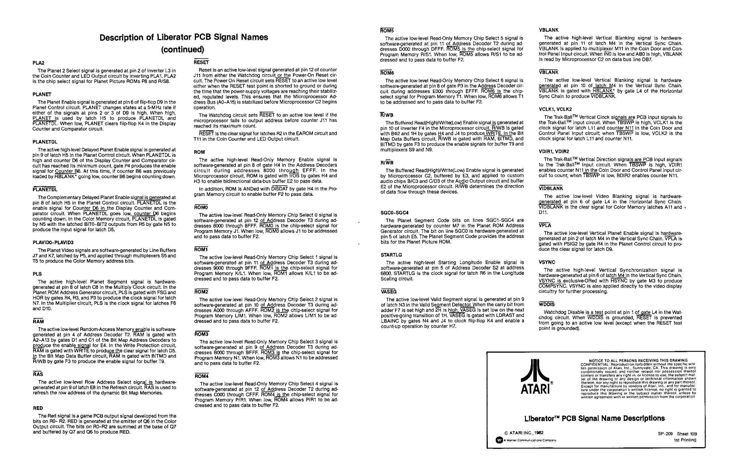
Description of Liberator PCB Signal Names
(continued)
PLA2 The Planet 2 Select signal is generated at pin 2 of inverter L3 in the Coin Counter and LED Output circuit by inverting PLA1. PLA2 is the chip select signal for Planet Picture ROMs P8 and R/S8,
PLANET The Planet Enable signal is generated at pin 6 of flip-flop D9 in the Planet Control circuit. PLANET changes states at a 5-MHz rate if either of the signals at pins 2 or 3 of 09 is high. When high, PLANET is used by latch H5 to produce PLANETDL and PLANETDL. When low, PLANET clears flip-flop K4 in the Display Counter and Comparator circuit.
PLANETDL
The active high-level Delayed Planet Enable signal is generated at
pin 9 of latch HS in the Planet Control circuit, When PLANETDL is high and counter D6 of the Display Counter and Comparator circuit has reached its minimum count, gate P4 produces the enable signal tor Counter B6. At this time, if counter B6 was previously loaded by HBLANK* going low, counter B6 begins counting down.
PLANETDL
‘The Complementary Delayed Planet Enable signal is generated at pin 8 of latch H5 in the Planet Control circuit. PLANETDL is the enable signal for Counter D6 in the Display Counter and Comparator circuit. When PLANETDL goes low, counter D6 begins counting down. In the Color Memory circuit, PLANETDL is gated by N& with the latched BITO-BIT2 outputs from RS by gate NS to. produce the input signal for latch DS.
PLAVIDO-PLAVIDS The Planet Video signals are software-generated by Line Buffers J7 and K7, latched by PS, and applied through multiplexers $5 and TS to produce the Color Memory address bits.
PLS The active hightevel Planet Segment signal is hardware. generated at pin 8 of latch C8 in the Multiply Clock circuit, In the Planet ROM Address Generator circuit, PLS is gated with FSG and HOR by gates R4, R3, and P3 to produce the clock signal for atch 'N7. tn the Multiplier circuit, PLS is the clock signal for latches F6 and D10.
RAM The active low-level Random-Access Memory enable is softwaregenerated at pin 4 of Address Decoder T2. RAM is gated with A2-A13 by gates D1 and C1 of the Bit Map Address Decoders to roduce the enable signal for E4. In the Write Protection circuit, is gated with WRITE to produce the clear signal for latch DS. ip the Bit Map Data Buffer circuit, RAM is gated with BITMD and R/WB by gate F3 to produce the enable signal for buffer T9.
RAS The active low-level Row Address Select signalis hardwaregenerated at pin 9 of latch E8 in the Refresh circuit. RAS is used to refresh the row address of the dynamic Bit Map Memories,
RED The Red signal is a game PCB output signal developed trom the bits on RO- R2. RED is generated at the emitter of Q6 in the Color Output circuit. The bits on RO-R2 are summed at the base of Q7 and buffered by Q7 and Q6 to produce RED. RESET Reset is an active low-level signal generated at pin 12 of counter 341 from either the Watchdog circuit_or the Power-On Reset circuit. The Power-On Reset circuit sets RESET to an active low level either when the RESET test point is shorted to ground or during the time that the power-supply voltages are reaching their stabilized, regulated levels. This ensures that the Microprocessor Ad-
dress Bus (A0-A 15) is stabilized before Microprocessor ©2 begins
operation, The Watchdog circuit sets RESET to an active low tevel if the microprocessor fails to output address before counter J11 has reached its maximum count. RESET is the clear signal for latches R2 in the EAROM circuit and T11 in the Coin Counter and LED Output circuit.
ROM The active high-level Read-Only Memory Enable signal is software-generated at pin 8 of gate H4 in the Address Decoders circuit during addresses 8000 through EFFF. In the Microprocessor circuit, ROM is gated with 1/08 by gates H4 and H3 to enable bidirectional data-bus buffer E2 to pass data. In addition, ROM is ANDed with DISDAT by gate H4 in the Program Memory circuit to enable buffer F2 to pass data.
ROMO The active low-level Read-Only Memory Chip Select 0 signal is software-generated at pin 12 of Address Decoder T3 during addresses 8000 through 8FFF. ROMO is the chip-select signal tor Program Memory J1. When low, ROMO allows J1 to be addressed and to pass data to buffer F2.
ROM1 The active low-level Read-Only Memory Chip Select 1 signal is software-generated at pin 11 of Address Decoder T3 during addresses 9000 through 9FFF. ROM1 is the chip-select signal for Program Memory K/L1. When low, ROM1 allows K/L1 to be addressed and to pass data to buffer F2.
Rom2 The active low-level Read-Only Memory Chip Select 2 signal is software-generated at pin 10 of Address Decoder T3 during ad- Gresses AQ0O through AFFF. ROM2 is the chip-select signal for Program Memory LiM1. When low, ROM2 allows L/M1 to be addressed and to pass data to buffer F2.
ROMS The active low-level Read-Only Memory Chip Select 3 signal is software-generated at pin 9 of Address Decoder T3 during addresses B000 through BFFF. ROMS is the chip-select signal for Program Memory N1. When low, ROMS allows N1 to be addressed and to pass data to buffer F2.
ROM4 The active low-level Read-Only Memory Chip Select 4 signal is software-generated at pin 12 of Address Decoder T2 during addresses C000 through CFFF. ROM4_is the chip-select signal for Program Memory P/R1. When low, ROM4 allows P/R1 to be addressed and to pass data to buffer F2. ROMs The active low-level Read-Only Memory Chip Select 5 signal is software-generated at pin 11 of Address Decoder T2 during addresses D000 through DFFF. ROMS is the chip-select signal for Program Memory R/S1. When low, ROMS allows R/S1 to be addressed and to pass data to butter F2.
ROM6 The active tow-level Read-Only Memory Chip Select 6 signal is software-generated at pin 8 of gate P3 in the Address Decoder circuit during addresses E000 through EFFF. ROM6 is the chipselect signal for Program Memory T1. When low, ROM6 allows T1 to be addressed and to pass data to buffer F2.
BiwB The Buffered Read(High)/Write(Low) Enable signal is generated at pin 10 of inverter F4 in the Microprocessor circuit. R/WB is gated
with B®2 and 1H by gates H4 and J4 to produce WRITE. In the Bit
Map Data Buffers circuit, R/WB is gated with RAM, BITMD, and BITMD by gate F to produce the enable signals for buffer T9 and multiplexers S9 and N9.
RIWB The Butfered Read(High)/Write(Low) Enable signal is generated by Microprocessor C2, buffered by E3, and applied to custom audio chips B/C3 and C/D3 of the Audio Output circuit and buffer E2 of the Microprocessor circuit. RWB determines the direction of data flow through these devices.
$GC0-SGC4 The Planet Segment Code bits on lines SGC1-SGC4 are hardware-generated by counter M7 in the Planet ROM Address Generator circuit. The bit on line SGCO is hardware-generated at pin 5 of latch E5. The Planet Segment Code provides the address bits for the Planet Picture ROM.
STARTLG The active high-level Starting Longitude Enable signal is software-generated at pin 5 of Address Decoder $2 at address 6800. STARTLG is the clock signa for latch R6 in the Longitude Sealing circuit,
VASEG The active low-level Valid Segment signal is generated at pin 9 ‘of latch N3 in the Valid Segment Detector. When the carry bit from adder F7 is set high and 2H is high, VASEG is set low on the next positive-going transition of 1H. VASEG is gated with LORAST and LBAINC by gates N4 and J4 to clock flip-flop K4 and enable a count-up operation by counter H7.
A,
ATARI
VBLANK The active high-level Vertical Blanking signa! is hardwaregenerated at pin 11 of latch M4 in the Vertical Syne Chain. VBLANK is applied to multiplexer M11 in the Coin Door and Control Panel Input circuit. When INO is low and ABO is high, VBLANK is read by Microprocessor C2 on data bus line DB7.
VBLANK
The active low-level Vertical Blanking signal is hardwaregenerated at pin 10 of_tatch M4 in the Vertical Sync Chain. VBLANK is gated with HBLANK* by gate L4 of the Horizontal Sync Chain to produce VIDBLANK.
VCLK1, VCLK2 The Trak-Ball™ Vertical Clock signals are PCB input signals to the Trak-Ball™ Input circuit. When TBSWP is high, VCLK1 is the clock signal for latch 111 and counter N11 in the Coin Door and Control Panel input circuit; when TBSWP is low, VCLK2 is the clock signal for latch L11 and counter N11.
VDIR1, VDIR2 The Trak-Ball™ Vertical Direction signals are PCB input signals to the Trak-Ball™ Input circuit. When TBSWP is high, VDIR1 enables counter N11 in the Coin Door and Control Panel Input circuit to count; when TBSWP is low, BDIR2 enables counter N11.
VIDBLANK
The active low-level Video Blanking signal is hardwaregenerated at pin 6 of gate L4 in the Horizontal Syne Chain. VIDBLANK is the clear signal for Color Memory latches A11 and D11.
VPLA The active iow-level Vertical Planet Enable signal is hardwaregenerated at pin 2 of latch Mé in the Vertical Sync Chain. VPLA is gated with PSIG2 by gate Ra in the Planet Gontrol circuit to produce the clear signa! for latch D9.
VSYNC The active high-level Vertical Synchronization signal is hardware-generated at pin 6 of latch Md in the Vertical Sync Ghain, VSYNC is exclusiveORed with HSYNC by gate M3 to produce COMPSYNG. VSYNC is aiso applied directly to the video display circuitry for further processing.
WODIS. Watchdog Disable is a test point at pin 1 of gate L4 in the Watchdog circuit. When WDDIS is grounded, RESET is prevented from going to an active low level (except when the RESET test point is grounded).
NOTICE TO ALL PERSONS RECEIVING THIS ORAWING CONFIDENTIAL: Reproduction forbidden without the specific wrt ten permission of Alan, Inc., Sunnyvale, CA, This drawing is only condilionally issued, and newther receipt nor possession thereol conlers oF transfers any right 4n, oF license to use, the subject mat ter of the drawing or any design or technical information shown thereon, nor any right lo reproduce this drawing or any part Ihereot. Excep! for manufacture by vendors of Atari, Inc., and lor manulac. ture under the corporalion’s written license, no right 1s granted to reproduce this drawing of the subject matier theceol. unless by weilien agreement with of weilten permission irom the corporation
Liberator™ PCB Signal Name Descriptions
© ATARIING., 1962 SP-209 Sheet 108 A warner Communications Company ist Printing
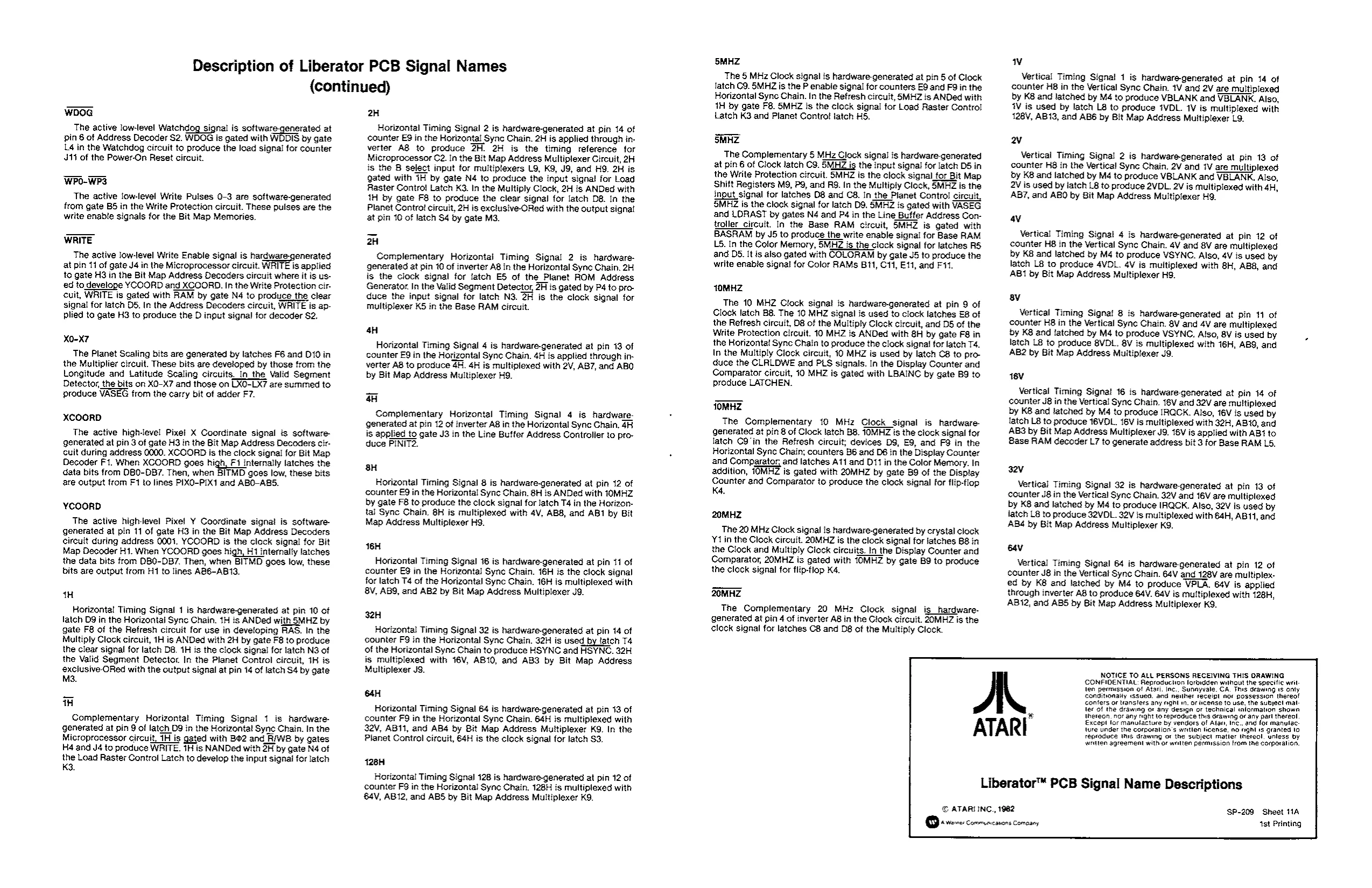
Description of Liberator PCB Signal Names
(continued)
wWboG The active low-level Watchdog signal is sottware-generated at pin 6 of Address Decoder $2. WDOG is gated with WDDIS by gate Lé in the Watchdog circuit to produce the load signal for counter 14 of the Power-On Reset circuit.
‘WPO-WP3
The active low-level Write Pulses 0-3 are software-generated from gate BS in the Write Protection circuit. These pulses are the write enable signals for the Bit Map Memories.
WRITE The active low-level Write Enable signal is hardware-generated at pin 11 of gate J4 in the Microprocessor circuit. WRITE is applied to gate H3 in the Bit Map Address Decoders circuit where it is used to develope YCOORD and XCOORD. In the Write Protection circuit, WRITE is gated with RAM by gate N4 to produce the clear signal for latch D5. In the Address Decoders circuit, WRITE is applied to gate H3 to produce the D input signal for decoder $2.
X0-X7 The Planet Scaling bits are generated by latches F6 and D10 in the Multiplier circuit. These bits are developed by those from the Longitude and Latitude Sealing circuits_lo_the Valid Segment Detector, the bits on X0-X? and those on LXO-LX7 are summed to produce VASEG from the carry bit of adder F7.
XCOORD
The active high-level Pixel X Coordinate signal is softwaregenerated at pin 3 of gate H3 in the Bit Map Address Decoders circuit during address 0000. XCOORD is the clock signal for Bit Map Decoder F1. When XCOORD goes high, Fi internally latches the data bits from DB0-DB7. Then, when BITMD goes low, these bits are output from F1 to lines PIXO-PIX1 and ABO-A85.
YCOORD The active high-level Pixel! Y Coordinate signat is software generated at pin 11 of gate H3 in the Bit Map Address Decoders circuit during address 0001. YCOORD is the clock signal for Bit Map Decoder H1. When YCOORD goes high, H1 internally latches the data bits from DBO-DB7. Then, when BITMD goes low, these bits are output from H1 to lines AB6-AB13_
1H
Horizontal Timing Signal 1 is hardware-generated at pin 10 of
latch D9 in the Horizontal Sync Chain. 1H is ANDed with SMHZ by
gate F8 of the Refresh circuit for use in developing RAS. In the Multiply Clock circuit, 1H is ANDed with 2H by gate F8 to produce the clear signal for latch D8. 1H is the clock signal for latch N3 of the Valid Segment Detector In the Planet Control circuit, 1H is exclusive-ORed with the output signal at pin 14 of latch S4 by gate M3.
TH
Complementary Horizontal Timing Signal 1 is hardwaregenerated at pin 9 of latch D9 in the Horizontal Syne Chain. In the Microprocessor circuit, 1H is gated with B62 and R/WB by gates 4 and J4 to produce WRITE. tH is NANDed with 2H by gate Né of the Load Raster Control Latch to develop the input signal for latch K3. 2H
Horizontal Timing Signal 2 is hardware-generated at pin 14 of counter E9 in the Horizontal Syne Chain. 2H is applied through inverter AB to produce 2H. 2H is the timing reference for Microprocessor C2. In the Bit Map Address Multiplexer Circuit, 2H is the B select input for multiplexers L9, K9, J9, and H9. 2H is gated with TH by gate Né4 to produce the input signal for Load Raster Contro! Latch K3. In the Multiply Clock, 2H is ANDed with 1H by gate F8 to produce the clear signal for latch D8. In the Planet Contro! circuit, 2H is exclusive-ORed with the output signal at pin 10 of latch S4 by gate M3.
2H Complementary Horizontal Timing Signal 2 is hardwaregenerated at pin 10 of inverter A8 in the Horizontal Syne Chain. 2H
is the clock signal for latch E5 of the Planet ROM Address
Generator. In the Valid Segment Detector, 2H is gated by P4 to produce the input signal for latch N3. 2H is the clock signal for multiplexer K5 in the Base RAM circuit.
4H Horizontal Timing Signal 4 is hardware-generated at pin 13 of counter E9 in the Horizontal Sync Chain. 4H is applied through inverter A8 to produce 4H. 4H is multiplexed with 2V, AB7, and ABO by Bit Map Address Multiplexer H9_
4H
Complementary Horizontal Timing Signal 4 is hardwaregenerated at pin 12 of inverter A8 in the Horizontal Sync Chain. 4H is applied to gate J3 in the Line Buffer Address Controller to produce PINIT2.
8H Horizontal Timing Signal 8 is hardware-generated at pin 12 of
counter £9 in the Horizontal Sync Chain. 8H is ANDed with 10MHZ
by gate F8 to produce the clock signal for latch T4 in the Horizontal Sync Chain. 8H is multiplexed with 4V, AB8, and AB1 by Bit Map Address Multiplexer H9.
16H Horizontal Timing Signal 16 is hardware-generated at pin 11 of counter E9 in the Horizontal Sync Chain. 16H is the clock signal for latch T4 of the Horizontal Sync Chain. 16H is multiplexed with 8V, AB9, and AB2 by Bit Map Address Multiplexer J9.
32H Horizontal Timing Signal 32 is hardware-generated at pin 14 of counier F9 in the Horizontal Sync Chain. 32H is used by latch T4 of the Horizontal Sync Chain to produce HSYNC and HSYNG. 32H is multiplexed with 16V, AB10, and AB3 by Bit Map Address Multiplexer J9.
64H
Horizontal Timing Signal 64 is hardware-generated at pin 13 of counter F9 in the Horizontal Syne Chain. 64H is multiplexed with 32V, ABIt, and AB4 by Bit Map Address Multiplexer KQ. In the Pianet Conirol circuit, 64H is the clock signal for latch $3.
128H
Horizontal Timing Signal 128 is hardware-generated al pin 12 of counter F¢ in the Horizontal Sync Chain. 128H is multiplexed with 64V, AB12, and ABS by Bit Map Address Multiplexer K9. SMHZ The 5 MHz Clock signal is hardware-generated at pin 5 of Clock latch C9. SMHZ is the P enabie signal for counters E9 and F9 in the Horizontal Sync Chain. In the Refresh circuit, SMHZ is ANDed with 1H by gate F8. SMHZ is the clock signal for Load Raster Control Latch K3 and Planet Controt latch H5.
SMAZ The Complementary 5 MHz Clock signal is hardware-generated at pin 6 of Clock latch C9. 5MHZ is the input signal for latch D5 in the Write Protection circuit. 5MHZ is the clock signal for Bit Map Shift Registers M9, P9, and RS. In the Multiply Clock, SMAZ is the input, signal for latches 08 and C8. In the Planet Control circuit, 5MHZ is the clock signal for latch D9. SMHZ is gated with VASEG and LDRAST by gates Né and P4 in the Line Buffer Address Controller_circuit. In the Base RAM circuit, 5MHZ is gated with BASRAM by J5 to produce the write enable signal for Base RAM LS. In the Color Memory, 5MHZ is the clock signal for latches RS and D8. It is also gated with COLORAM by gate J5 to produce the write enable signal for Color RAMs Bit, C11, E11, and Fit.
1OMHZ
The 10 MHZ Clock signa! is hardware-generated at pin 9 of Clock latch B8. The 10 MHZ signal is used to clock latches E8 of the Refresh circuit, D8 of the Multiply Clock circuit, and D5 of the Write Protection circuit. 10 MHZ is ANDed with 8H by gate F8 in the Horizontat Sync Chain to produce the clock signa! for latch T4. In the Multiply Clock circuit, 10 MHZ is used by latch C8 to produce the CLRLDWE and PLS signals. In the Display Counter and Comparator circuit, 10 MHZ is gated with LBAINC by gate BS to produce LATCHEN.
1OMHZ The Complementary 10 MHz Clock signal is hardwaregenerated at pin 8 of Clock latch B8. 1OMHZ is the clock signal for latch C9’in the Refresh circuit; devices D9, E9, and F8 in the Horizontal Syne Chain; counters 86 and D6 in the Display Counter and Comparator, and latches Ait and D11 in the Color Memory. In addition, {MHZ is gated with 20MHZ by gate B9 of the Display Counter and Comparator to produce the clock signal for flip-flop Ka.
20MHZ The 20 MHz Clock signal is hardware-generated by crystal clock Y1 in the Clock circuit. 20MHZ is the clock signal for latches B8 in the Clock and Multiply Clock circuits. In the Display Counter and Comparator, 20MHZ is gated with 1OMHZ by gate B9 to produce the clock signal for flip-flop K4.
20MHZ The Complementary 20 MHz Clock signal is_hardwaregenerated at pin 4 of inverter A8 in the Clock circuit. 20MHZ is the clock signal for latches C8 and D8 of the Multiply Clock.
ATARI
© ATARI ING, 1982 wv Vertical Timing Signal 1 is hardware-generated at pin 14 of counter H8 in the Vertical Sync Chain. 1V and 2V are multiplexed by K8 and latched by Mé to produce VBLANK and VBLANK. Also, 4V is used by latch L8 to produce #VDL. 1V is multiplexed with 128V, AB13, and AB6 by Bit Map Address Multiplexer L9.
aw Vertical Timing Signal 2 is hardware-generated at pin 13 of counter H8 in the Vertical Sync Chain. 2V and V are multiplexed by K8 and latched by Mé to produce VBLANK and VBLANK. Also, 2¥ is used by iatch LB to produce 2VDL. 2V is muitiplexed with 4H, AB?, and ABO by Bit Map Address Multiplexer H9.
a
Vertical Timing Signal 4 is hardware-generated at pin 12 of counter H8 in the Vertical Sync Chain. 4V and 8V are multiplexed by K8 and latched by M4 to produce VSYNC. Also, 4V is used by latch L8 to produce 4VDL. 4V is muitiplexed with 8H, ABS, and ABI by Bit Map Address Multiplexer H9.
av
Vertical Timing Signa! 8 is hardware-generated at pin 11 of counter H8 in the Vertical Syne Chain. 8V and 4V are multiplexed by K8 and latched by M4 to produce VSYNC. Also, 8V is used by latch L8 to produce 8VDL. 8V is multiplexed with 16H, ABS, and AB2 by Bit Map Address Multiptexer J9.
18V
Vertical Timing Signa! 16 is hardware-generated at pin 14 of counter J8 in the Vertical Syne Chain. 16V and 32V are multiplexed
by K8 and latched by M4 to produce IRQCK. Also, 16V is used by
latch L8 to produce 16VOL. 16V is multipiexed with 32H, AB10, and ABS by Sit Map Address Multiplexer J9. 18V is applied with ABt to Base RAM decoder L7 to generate address bit 3 for Base RAM L5.
Vertical Timing Signal 32 is hardware-generated at pin 13 of counter J8 in the Vertical Sync Chain. 32V and 16V are multiplexed by K8 and latched by M4 to produce IRQCK. Also, 32V is used by latch L8 to produce 32VDL. 32V is multiplexed with 64H, AB11, and ABé by Bit Map Address Multiplexer K9.
Vertical Timing Signal 64 is hardware-generated at pin 12 of counter J8 in the Vertical Sync Chain. 64V and 128V are multiplexed by KB and latched by Md to produce VPLA. 64V is applied through inverter AB to produce 64V. 64V is multiplexed with 128H, ABI2, and AB5 by Bit Map Address Multiplexer K9.
NOTICE TO ALL PERSONS RECEIVING THIS ORAWING CONFIDENTIAL: Reproduction forbidden without the specific writ Ten permussion of Atari, Inc., Sunnyvale. CA. This Grawing 1s onty conditionally «sued. and neither receipl nor possession thereof confers or transfers any nighl in, of incense to use. the subject mal ler of the drawing or any design or technical mlormation shown thereon. nor any right lo reproduce this Grawing or any parl thereol Except lor manufacture by vendors of Alan, Inc., and for manulac: lure under the corporalion’s wiilen license, ao aghl 1s granted to reproduce Ins drawing or the subject matter thereol, unless by wrullen agreement with or walten permussion fram the corparalion.
Liberator™ PCB Signal Name Descriptions
SP-209 Sheet 114 «Heres Communcatons Company ‘st Printing
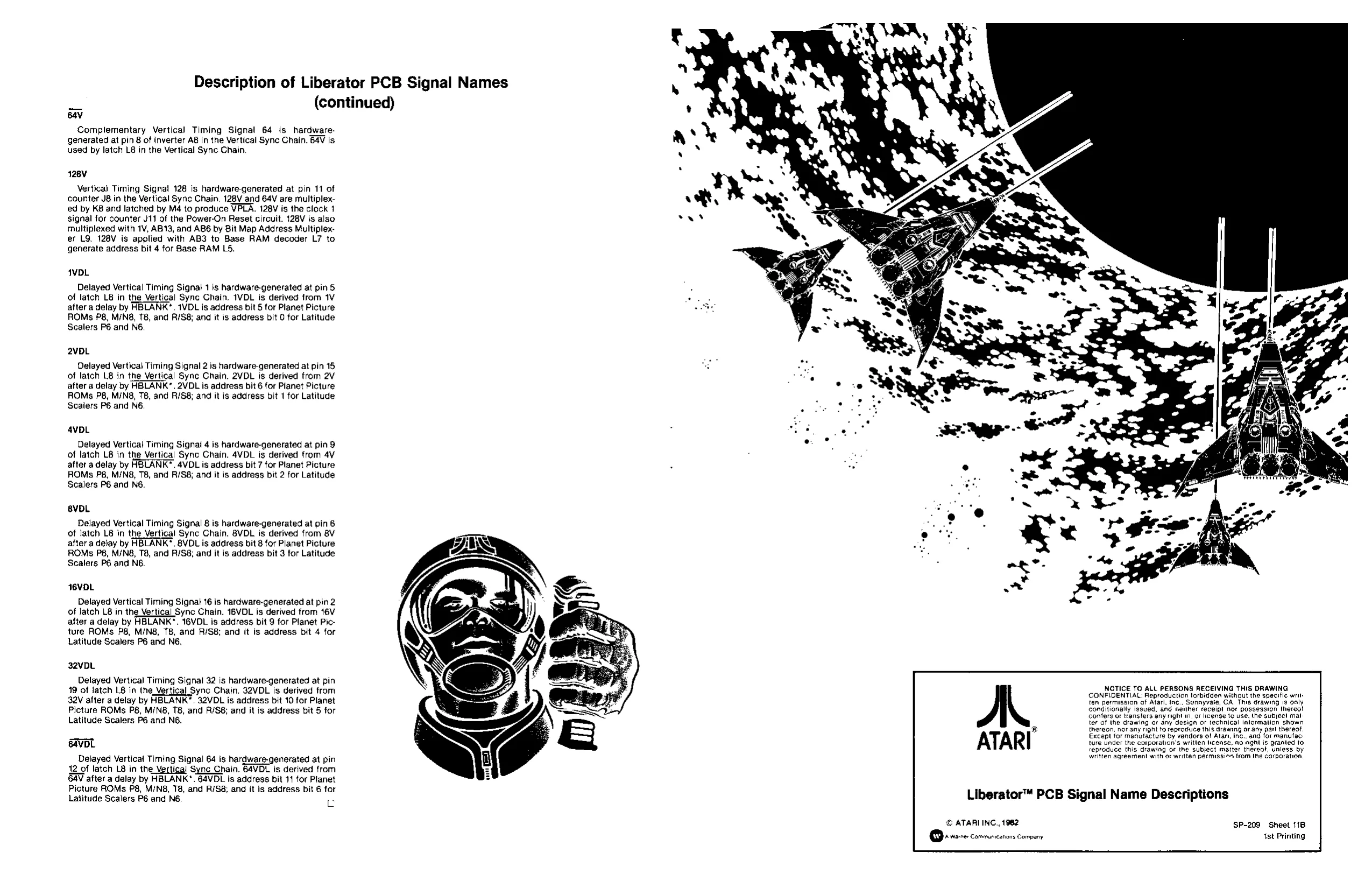
Description of Liberator PCB Signal Names
(continued)
64V
Complementary Vertical Timing Signal 64 is hardwaregenerated at pin 8 of inverter A in the Vertical Sync Chain. 64V is. used by latch L8 in the Vertical Sync Chain.
128V
Vertical Timing Signal 128 is hardware-generated at pin 11 of counter J8 in the Vertical Syne Chain, 128V and 64V are multiplexed by K8 and latched by M4 to produce VPLA. 128V is the clock 1 signal for counter J11 of the Power-On Reset circuit. 128V is also multiplexed with 1V, AB1, and AB6 by Bit Map Address Multiplex. er L9. 128V is applied with AB3 to Base RAM decoder L7 to generate address bit 4 for Base RAM LS.
VDL
Delayed Vertical Timing Signal 1 is hardware-generated at pin 5 of latch L8 in the Vertical Sync Chain. 1VDL is derived from 1V
after a delay by HBLANK®. 1VDL is address bit § for Planet Picture
ROMs P8, M/N8, T8, and R/S8; and it is address bit 0 for Latitude Scalers P6 and N6.
2VDL
Delayed Vertical Timing Signal 2 is hardware-generated at pin 15 of latch L8 in the Vertical Syne Chain. 2VDL is derived from 2V
after a delay by HBLANK’. 2VDL is address bit 6 for Planet Picture
ROMs P8, M/N8, T8, and R/S8; and it is address bit 1 for Latitude Scalers P6 and N6.
AVDL
Delayed Vertical Timing Signal 4 is hardware-generated at pin 9 of latch L8 in the Vertical Sync Chain. 4VDL is derived from 4V after a delay by HBLANK*. 4VDL is address bit 7 tor Planet Picture ROMs P8, M/N8, T8, and R/S8; and it is address bit 2 for Latitude Scalers P6 and N6.
8VOL
Delayed Vertical Timing Signal 8 is hardware-generated at pin 6 ‘ot latch L8 in the Vertical Sync Chain. 8VDL is derived from 8V after a delay by HBLANK™. 8VDL is address bit 8 for Planet Picture ROMs P8, M/N8, TS, and A/S8; and it is address bit 3 for Latitude Scalers P6 and N6.
16VDL
Delayed Vertical Timing Signa} 16 is hardware-generated at pin 2 of Jatch L8 in the Vertical Sync Chain. 1BVDL is derived from 16V after a delay by HBLANK*. 16VDL is address bit 9 for Planet Picture ROMs P8, M/N8, 78, and R/S8; and it is address bit 4 for Latitude Scalers P6 and N6.
32VDL
Delayed Vertical Timing Signal 32 is hardware-generated at pin 19 of latch LB in the Vertical Syne Chain. 32VDL is derived from 32V after a delay by BLANK’. 32VDL is address bit 10 for Planet Picture ROMs P8, M/N8, T8, and R/SE; and it is address bit 5 for Latitude Scalers P6 and N6.
confers or transfers any right in, or license to use, the subject mat
NOTICE TO ALL PERSONS RECEIVING THIS DRAWING CONFIDENTIAL; Reproduction torbidden without the specific wrt: ten permissian af Atari, inc., Sunnyvale, CA. This drawing 1s only conditionally issued, and neither receipt nor possession thereo!
ter of the drawing of any design oF technical information shown thereon, nor any right to reproduce this drawing or any parl thereot. & cent Excepl for manulacture by vendors of Atan, Ine. and for manufac eaVDL ture under the corporation's written Weense, a0 rghl is granted (0 reproduce this drawing or the subject matter thereot, unless by Delayed Vertical Timing Signal 64 is hardware-generated at pin written agreement with or written permission trom Ihe Corporation, 12 of latch 18 in the Vertical Sync Chain. 64VDL is derived from 64V after a delay by HBLANK*. 64VDL is address bit 11 for Planet Picture ROMs P8, M/N8, T8, and R/S8; and it is address bit 6 for Latitude Scalers P6 and N6. ts Liberator™ PCB Signal Name Descriptions
© ATARI ING., 1962 SP-209 Sheet 116 + tere: commumeatons Company Ist Printing
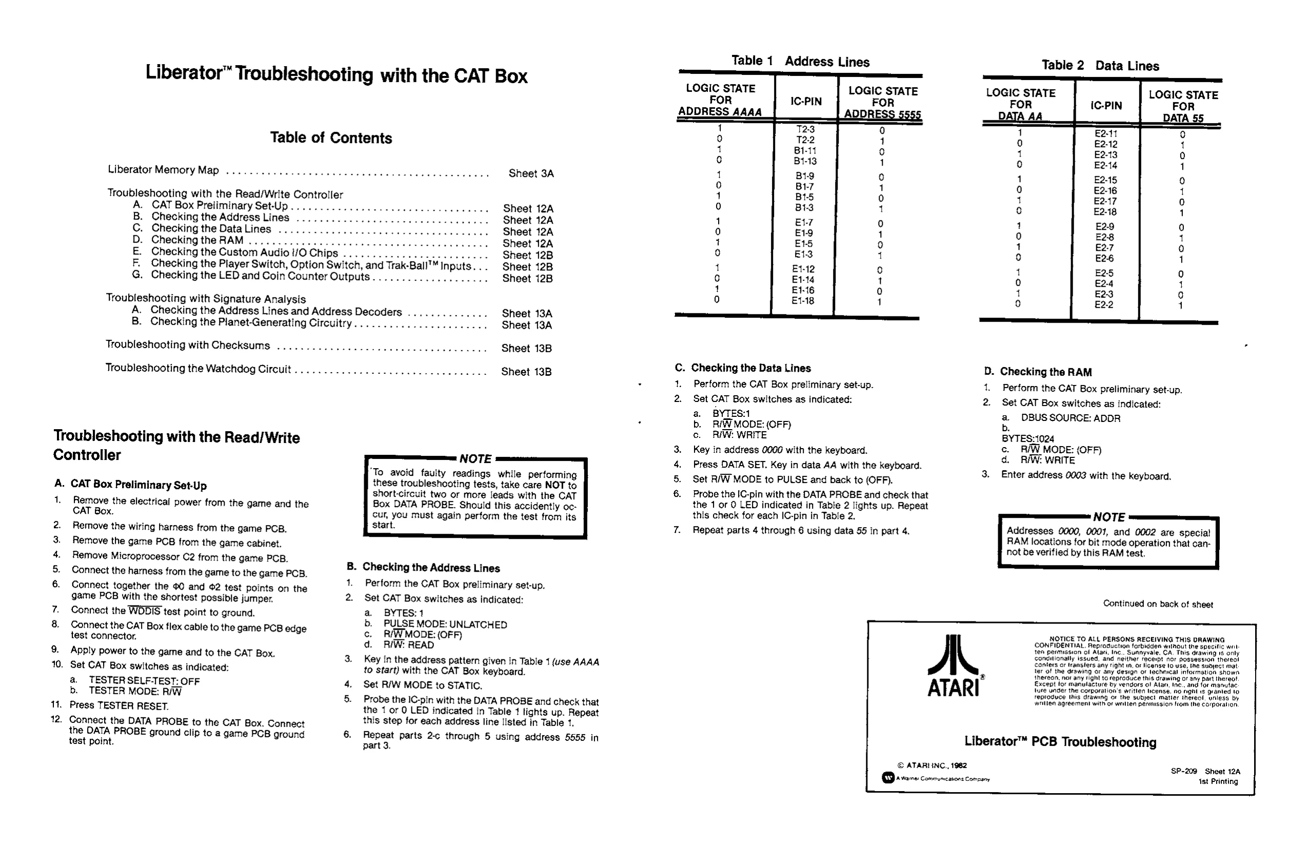
Liberator™ Troubleshooting with the CAT Box
1 Q 1 0 Table of Contents H 4 7 t 0 1 Oo 1 Liberator Memory Map .... 2.0... eee ccc ee ce eee seeceececcenens Sheet 3A é 0 1 9 1 ie) 1 Troubleshooting with the Read/Write Controller 4 0 1 0 A. CAT Box Preliminary Set-Up ....... Sheet 12A 1 ° 1 B. Checking the Address Lines Sheet 12A 1 0 1 0 C. Checking the DataLines .. Sheet 124 0 1 ty) 1 D. Checking the RAM Sheet 124 3 9 1 0 E. Checking the Custom Audio i/O Chips Sheet 128 1 9 1 F. Checking the Player Switch, Option Switch, and Trak-Ball™ Inputs Sheet 12B 1 0 1 0 G. Checking the LED and Coin Counter Outputs.................... Sheet 12B H 3 ° 4 Troubleshooting with Signature Analysis a 1 9 1 A. Checking the Address Lines and Address Decoders . . Sheet 13A B. Checking the Planet-Generating Circuitry Sheet 134A
Troubleshooting with Checksums ......2....00.00 000 ccu ce eeeeeeeeceee Sheet 13B Troubleshooting the Watchdog Circuit ..... 2.2.0... ccc cece eee eee Sheet 13B C. Checking the Data a | D. Checking the RAM
- Pertorm the CAT Box preliminary set-up. 1. Perform the CAT Box preliminary set-up.
- Set CAT Box switches as indicated: 2. Set CAT Box switches as indicated: a. BYTES:1 a. DBUS SOURCE: ADDR b. R/W MODE: (OFF) b. ' . . co. RIW: WRITE BYTES:1024 Troubleshooting with the Read/ Write 3. Key in address 0000 with the keyboard. é AN wae {OFF) Controller NOTE 4. Press DATA SET. Key in data AA with the keyboard. 3. &: : dal 0003 with the keyboard "To avoid faulty readings while performing 5. Set R/W MODE to PULSE and back to (OFF). me Enter adcress bal 'e Keyboard, A. CAT Box Preliminary Set-Up chorale tne “or more ieads with the GAT 6. Probe the IC-pin with the DATA PROBE and check that 1, Remove the electrical power from the game and the Box DATA PROBE. Should this accidently oc- the 1 or 0 LED indicated in Table 2 lights up. Repeat NOTE CAT Box. cur, you must again perform the test from its this check for each IC-pin in Table 2. aia 0001, and 0002 ia irk Start. 7. Repeat parts 4 through 6 using data 55 in part 4. resses 9000, , an are special
- Remove the wiring harness from the game PCB. ‘epeat parts: o 8 p RAM locations for bit mode operation that can-
- Remove the game PCB from the game cabinet. not be verified by this RAM test.
- Remove Microprocessor C2 from the game PCB. +
- Connect the harness from the game to the game PCB. . ee ime neeress Lines . hi the ox preliminary set-up.
- Connect together the 00 and 2 test points on the ebb i game PCB with the shortest possible jumper. 2. Set CAT Box switches as indicated: Continued on back of sheet
- Connect the WODIS test point to ground. a. BYTES:1
- Connect the CAT Box flex cable to the game PCB edge test connector,
- Apply power to the game and to the CAT Box.
- Set CAT Box switches as indicated: a. TESTER SELF-TEST: OFF b. TESTER MODE: RAW
- Press TESTER RESET.
- Connect the DATA PROBE to the CAT Box. Connect the DATA PROBE ground clip to a game PCB ground test point. b. PULSE MODE: UNLATCHED c. R/WMODE: (OFF) d. RIW: READ
- Key in the address pattern given in Table 1 (use AAAA to start) with the CAT Box keyboard.
- Set R/W MODE to STATIC. Probe the IC-pin with the DATA PROBE and check that the 1 or 0 LED indicated in Table 1 lights up. Repeat this step for each address line listed in Table 1.
- Repeat parts 2-c¢ through 5 using address 5555 in part 3. Table 1 Address Lines Table 2 Data Lines
LOGIC STATE LOGIC STATE LOGIC STATE LOGIC STATE FOR FOR FOR ADDRESS AAAA DATA AA DATA 5:
AL ATARI NOTICE TO ALL PERSONS RECEIVING THIS DRAWING CONFIDENTIAL, Reproduction forbidden without the specific wat ten permission of Alar, Inc... Sunnyvale. CA. This drawing 18 only conditionally issued, and neither receipt nor possession thereo! conlers or transters any right in. or license to use, tne subject mat ter of the drawing or any design oF technical information shown {hereon nor any right 10 reproduce this drawing or any part thereo! Except for manulacture by vendors of Alar, Ine., and for manufac lure unger the corporation's writlen license. no Hgnl v8 granted 10 reproduce this drawing ot the subject matier thereol. unless by wiitien agreement with or wrilien permission ftom the Corporation
Liberator™ PCB Troubleshooting
© ATARIINC., 1962 pr reresconmncstne Canon SP-209 Sheet 128 ist Printing
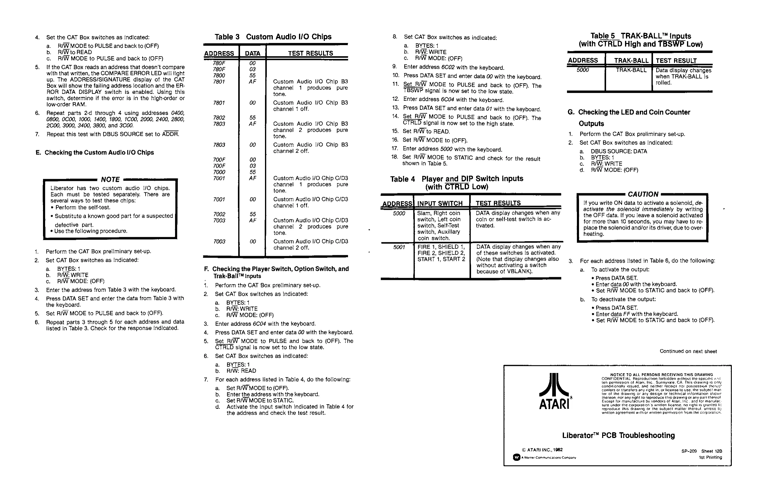
| 4, | Set the CAT Box switches as indicated: | Table 3 | Custom Audio I/O Chips | 8 | Set CAT Box switches as indicated: | Table 5_ TRAK-BALL™ inputs | ||||
| a. | R/WMODE to PULSE and back to (OFF) | a. | BYTES:1 | (with CTRLD High and TBSWP | Low) | |||||
| ee | Le ee | een ee | ee | TEST RESULTS | RW MODS | |||||
| : | ° Bikes | - | eon | = a | . | 3 | . | 'W MODE: (OFF) | ADDRESS | TRAK-BALL | TEST RESULT |
| a | the | ox reads an address that doesn’t compare | a | nter address 6C02 with the keyboard. | SS | |||||
| with that written, the COMPARE ERROR LED wil light | 40. Press DATA SET | and | yoial | 5000 | TARBALL | Data display changes | |||||
| up. The ADDRESS/SIGNATURE display of the CAT | Custom Audio VO Chip | B3 | . | DA | and enter data 00 with the keyboard. | when TRAK-BALL is. | ||||
| Box will show the failing address location and the ER- | channel | 1 | produces Pure | 11. Set RAW MODE to PULSE and back to (OFF). The | na | |||||
| ROR DATA DISPLAY switch is enabled. Using this | tone. | TBSWP signal is now set to the low state. | ||||||||
| switch, determine if the error is in the high-order or | ” | z | i | |||||||
| jeweler RAW | ig | 7801 | Custom Audio VO Chip B3 | 5 ain pres 6C04 with the keyboard. | ||||||
| . | Press | fA SET | i | a | A | |||||
| 6. | Repeat parts 2-d through 4 using addresses 0400, | channel. | Toff | pans | and enter data 07 with the keyboard. | G. Checking the LED and Coin Counter | ||||
| 0800, C00, 1000, 1400, 1800, 1000, 2000, 2400, 2800, | 7802 | 14. Set RAW MODE | to PULSE and back to (OFF). The | |||||||
| 2C00, 3000; 3400, 3800, and 3C00. | 7803 | Custom Audio 1/0 Chip B3 | CTRLD signal is now set to the high state. | Outputs | ||||||
| 7, | Repeat this test with DBUS SOURCE set to ADDR. | channel 2 produces pure | 18. Set R/W to READ. | 1, | Perform the CAT Box preliminary set-up. | |||||
| 7803 | Custom Audio 1/0 Chip B3 | . a ae | pecs te (OFF). | 2. | Set CAT Box switches as indicated: | |||||
| E. Checking the Custom Audio I/O Chips | channel 2 off. | ~ | Enter address 5000 with the keyboard. | a, | DBUS SOURCE: DATA | |||||
| v00F | 18. Set R/W MODE to STATIC and check for the result | b. | BYTES: 1 | |||||||
| SOOE | shown in Table 6. | c. | RIW: WRITE | |||||||
| 7000 | d. | RIW MODE: (OFF) | ||||||||
| NOTE | 7001 | Custom Audio vo Chip C/D3 | Table 4 | Player and DIP Switch Inputs | ||||||
| Liberator has two custom audio 1/0 chips. | chanie | produces: pure | (with CTRLD Low) | |||||||
| Each must be tested separately. There are | 7001 | c | " | Audiol Chip GDS | CAUTION | |||||
| Several ways to test these chips: | Leto | 7 | ADDRESS! INPUT SWITCH | If you write ON data to activate a solenoid, de- | ||||||
| * Perform the self-test | channel 1 off. | hie: | ; | a | ‘ | " ¢ | ||||
| . | SI | Right | " | DATA displ | ni | Th | activate the solenoid immediately by writing | |||
| Substitute a known good part for a suspected | 7002 | . | | | $000 | jam, | Right coin | isplay | changes when any | the OFF data. If you leave a solenoid activated | |
| . | 7003 | Custom Audio I/O Chip C/D3 | switch, Lett coin | coin or self-test switch is ac- | for more | than 10 | di | have | to | re- |
| defective part. | channel 2 produces pure | switch, Self Test | tivated. | plage the solenoid andlor itSdriver-due to over |
* Use the following procedure. tone. switch, Auxillary heating. ‘
| 7003 | Custom Audio 10 Chip C/D3 | isl — Sn | SRS | - |
| A | channel 2 off. | FIRE 1, | isplay | changes when any |
| 1. | Perform the CAT Box preliminary set-up. | * | FIRE 2, SHIELD 2, | of these switches is activated. | |
| START 1, START 2 | (Note that display changes also | 3, | For each address listed in Table 6, do the following: |
without activating a switch a. To activate the output: because of VBLANK).
- Press DATA SET.
- Enter data 00 with the keyboard.
- Set R/W MODE to STATIC and back to (OFF).
- Set CAT Box switches as indicated:
| a. | BYTES:1 | F. Checking the Player Switch, Option Switch, and | ||||
| b. | RAW: WRITE | Trak-Ball™ Inputs. | ||||
| & | RW MODE: (OFF) | 4. | Perform | the GAT Sox | preliminary set-u | |
| . | ertorm | UP. | ||||
| 3, | Enter the address from Table 3 with the keyboard. | . | “Pe | . " | 2 | P |
- Set CAT Box switches as indicated:
| 4, | Press DATA SET and enter the data from Table 3 with | b. | To deactivate the output: | |
| the keyboard. | a | BYTES:1 | p | |
| ba | b. | RAW: | WRITE | + Press DATA SET. |
| 5. | Set RW MODE to PULSE and back to (OFF). | c. | RW MODE: (OFF) | * Enter data FF with the keyboard. |
| 6. | Repeat parts 3 through 5 for each address and data | 3. | Enter address 6C04 with the keyboard. | * Set R/W MODE to STATIC and back to (OFF). |
listed in Table 3. Check for the response indicated.
| "Ste in tere | p | 4. | Press DATA SET and enter data 00 with the keyboard. |
Set RAW MODE to PULSE and back to (OFF). The CTRLD signal is now set to the low state.
- Set CAT Box switches as indicated: a. BYTES:1 b. RW: READ
| a | + | . | NOTICE TO ALL PERSONS AECEIVING THIS DRAWING |
| 7. | For each address listed in Table 4, do the following: | CONFIDENTIAL Reproduction forbidden without Ine specilsc |
Ww Ghndiionaly ssgued. shd neliner Tacepl nor possess
conditionally 1ssued, and neither receipt nor possession
| 8. | Set RW MODE to (OFF). | Gontars of wanetars ony ight ior ngage to wpa, he subject wat |
| . | Enter the address with the keyboard. | ter of the drawing or any design or technical information shiowr |
ATARI
Continued on next sheet
thereon, nor any right 10 reproduce this drawing oF any part (hereo!
Except for manufacture by vendors of Atari, Inc . and for manut
ture under the corporation's writen license, no right ts grantee to reproduce this drawing or the Subject matter Inereol, uniess by welten agreement with or wtten permission from the corpuraticn. b, c. Set RAW MODE to STATIC. d. Activate the input switch indicated in Table 4 for the address and check the test result.
Liberator™ PCB Troubleshooting
© ATARIINC., 1982 -ArWetaes Communcalions Company SP-209 Sheet 128 1st Printing
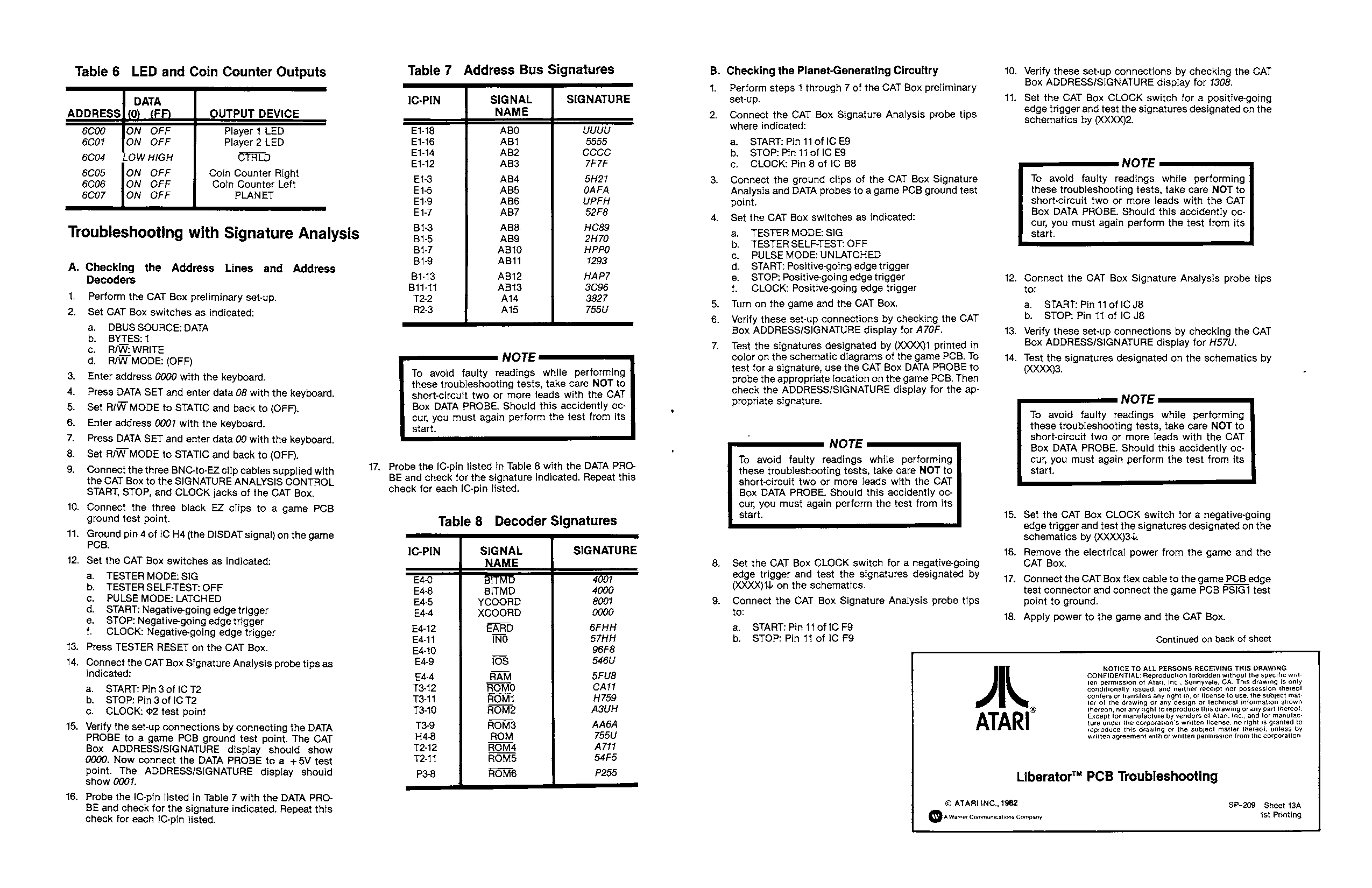
Table 6 LED and Coin Counter Outputs
DATA
ADDRESS. OUTPUT DEVICE
ION OFF Player 1 LED 6Cot Player 2 LED 6C04 CTRLD 6C05 Coin Counter Right 6C06 Coin Counter Left PLANET
Troubleshooting with Signature Analysis
A. Checking the Address Lines and Address Decoders
- Perform the CAT Box preliminary set-up.
- Set GAT Box switches as indicated: a. DBUS SOURCE: DATA b. BYTES:1 c. RIW: WRITE @. IW MODE: (OFF) Enter address 0000 with the keyboard. Press DATA SET and enter data 08 with the keyboard. Set RW MODE to STATIC and back to (OFF). Enter address 0007 with the keyboard. Press DATA SET and enter data 00 with the keyboard. Set R/W MODE to STATIC and back to {OFF). Connect the three BNC-to-EZ clip cables supplied with the CAT Box to the SIGNATURE ANALYSIS CONTROL START, STOP, and CLOCK jacks of the CAT Box.
- Connect the three black EZ clips to a game PCB ground test point.
- Ground pin 4 of IC H4 (the DISDAT signal) on the game PCB. PO PNMAaALw
- Set the CAT Box switches as indicated: TESTER MODE: SIG TESTER SELF-TEST: OFF PULSE MODE: LATCHED START: Negative-going edge trigger STOP: Negative-going edge trigger CLOCK: Negative-going edge trigger
- Press TESTER RESET on the CAT Box. spaoge
- Connect the CAT Box Signature Analysis probe tips as.
15,
16. indicated: a. START: Pin 3 of iC T2 b. STOP: Pin 3 of IC T2 ¢. CLOCK: $2 test point Verify the set-up connections by connecting the DATA PROBE to a game PCB ground test point. The CAT Box ADDRESS/SIGNATURE display should show 0000. Now connect the DATA PROBE to a +5V test point. The ADDRESS/SIGNATURE display should show 0001. Probe the IC-pin listed in Table 7 with the DATA PRO- BE and check for the signature indicated. Repeat this check for each IC-pin listed. Table 7 Address Bus Signatures
SIGNAL SIGNATURE NAME
- Probe the [C-pin listed in Table 8 with the DATA PRO- BE and check for the signature indicated. Repeat this check for each [C-pin fisted.
Table 8 Decoder Signatures
NAME
BITMD BITMD. YCOORD SIGNATURE . Checking the Planet-Generating Circuitry Perform steps 1 through 7 of the CAT Box preliminary set-up. Connect the CAT Box Signature Analysis probe tips where indicated: a. START: Pin 11 of (C E9 b. STOP: Pin 11 of IC ES c. CLOCK: Pin 8 of IC B& Connect the ground clips of the CAT Box Signature Analysis and DATA probes to a game PCB ground test point. Set the CAT Box switches as indicated: TESTER MODE: SIG TESTER SELF-TEST: OFF PULSE MODE: UNLATCHED START: Positive-going edge trigger STOP: Positive-going edge trigger CLOCK: Positive-going edge trigger Turn on the game and the CAT Box. Verify these set-up connections by checking the CAT Box ADDRESS/SIGNATURE display for A70F. reaps
Test the signatures designated by (XXX)}1 printed in color on the schematic diagrams of the game PCB. To test for a signature, use the CAT Box DATA PROBE to probe the appropriate location on the game PCB. Then check the ADDRESS/SIGNATURE display for the appropriate signature.
Set the CAT Box CLOCK switch for a negative-going edge trigger and test the signatures designated by (XXXX)1) on the schematics. Connect the CAT Box Signature Analysis probe tips to: a. START: Pin 11 of IC F9 b. STOP: Pin 11 of IC F9
A
ATARI
© ATARIING., 1982 Avwarner Commumcations Company tt. . Verify these set-up connections by checking the CAT Box ADDRESS/SIGNATURE display for 1308. Set the CAT Box CLOCK switch for a positive-going edge trigger and test the signatures designated on the schematics by 0000)2.
. Connect the CAT Box Signature Analysis probe tips to: a. START: Pin 11 of IC J8 b. STOP: Pin 11 of IC J8& . Verify these set-up connections by checking the CAT Box ADDRESS/SIGNATURE display for H57U, |. Test the signatures designated on the schematics by (XXXXS.
. Set the CAT Box CLOCK switch for a negative-going edge trigger and test the signatures designated on the schematics by (XXXxj3¥. Remove the electrical power from the game and the CAT Box. Connect the CAT Box flex cable to the game PCB edge test connector and connect the game PCB PSIG1 test point te ground. Apply power to the game and the CAT Box.
Continued on back of sheet
NOTICE TO ALL PERSONS RECEIVING THIS DRAWING. CONFIDENTIAL: Reproduction foridden without the specific wrt ten permission of Atati, Inc . Sunnyvale, CA. This drawing is only conditionally issued, and neither recespt nor possession thereot confers or Iranslers any right in, oF license to use, the subject mat ler of the drawing or any design or technical information shown thereon, nor any righ! 10 reproduce this drawing or any part Inerect. Except ior manufacture by vendors of Atari. (nc., and lor manutac: Ture under the corporation's wrilten license, no right 15 granted to reproduce this drawing or the subjecl matler inereol. unless by witten agreement with or wrilten permission from the corporation
Liberator™ PCB Troubleshooting
SP-209 Sheet 13A ist Printing
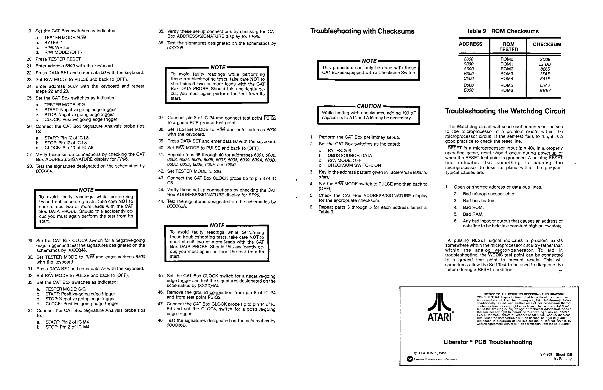
18.
20. 21. 22. 23. 24.
2.
26.
27.
28.
32. 33.
34. Set the CAT Box switches as indicated: a. TESTER MODE: RW b. BYTES:1 c. RAW: WRITE d. RAW MODE: (OFF) Press TESTER RESET. Enter address 6800 with the keyboard. Press DATA SET and enter data 00 with the keyboard. Set R/W MODE to PULSE and back to (OFF). Enter address 6CO7 with the keyboard and repeat steps 22 and 23. Set the CAT Box switches as indicated: a. TESTER MODE: SIG b. START: Negative-going edge trigger c. STOP: Negative-going edge trigger d. CLOCK: Positive-going edge trigger Connect the CAT Box Signature Analysis probe tips to: a. START: Pin 12 of ICL8 b. STOP: Pin 12 of fC L8 ¢. CLOCK: Pin 10 of IC AB Verify these set-up connections by checking the CAT Box ADDRESS/SIGNATURE display for FP96. Test the signatures designated on the schematics by {(XXXX)4.
. Set the CAT Box CLOCK switch for a negative-going edge trigger and test the signatures designated on the schematics by (XXXX)44. . Set TESTER MODE to R/W and enter address 6800 with the keyboard. Press DATA SET and enter data 7F with the keyboard. Set RAW MODE to PULSE and back to (OFF). Set the CAT Box switches as indicated: a. TESTER MODE: SIG b, START: Positive-going edge trigger c. STOP: Negative-going edge trigger d. CLOCK: Positive-going edge trigger Connect the CAT Box Signature Analysis probe tips to: a. START: Pin 2 of IC M4 b. STOP: Pin 2 of IC M4 35.
36.
47, Verify these set-up connections by checking the CAT Box ADDRESS/SIGNATURE display for FP96. Test the signatures designated on the schematics by {XXXX}S.
. Connect pin 8 of IC P4 and connect test point PSIG2 to a game PCB ground test point. Set TESTER MODE to R/W and enter address 6000 with the keyboard. Press DATA SET and enter data 00 with the keyboard. . Set RAW MODE to PULSE and back to (OFF). . Repeat steps 38 through 40 for addresses 6001, 6002, 6003, 6004, 6005, 6006, 6007, 6008, 6009, 600A, 600B, 600C, 600D, 600E, 600F, and 6800. Set TESTER MODE to SIG. Connect the CAT Box CLOCK probe tip to pin 8 of iC cB. |. Verify these set-up connections by checking the CAT Box ADDRESS/SIGNATURE display for FP96, |. Test the signatures designated on the schematics by A.
Set the CAT Box CLOCK switch for a negative-going edge trigger and test the signatures designated on the schematics by (XXXX}6AL. Remove the ground connection from pin 8 of IC P4 and from test point PSiG2. Connect the CAT Box CLOCK probe tip to pin 14 of IC EQ and set the CLOCK switch for a positive-going edge trigger. Test the signatures designated on the schematics by 00CaQSB.
Troubleshooting with Checksums
- Perform the CAT Box preliminay set-up.
- Set the CAT Box switches as indicated: a, BYTES: 256 b. DBUS SOURCE: DATA c. RAW MODE: OFF d. CHECKSUM SWITCH: ON
- Key in the address pattern given in Table 9 (use 8000 to Start).
- Set the R/W MODE switch to PULSE and then back to (OFF,
- Check the CAT Box ADDRESS/SIGNATURE display for the appropriate checksum.
- Repeat parts 3 through 5 for each address listed in Table 9.
© ATARI INC., 1982, rece communesions Comeonr Table 9 ROM Checksums
ROM TESTED ADDRESS CHECKSUM
Troubleshooting the Watchdog Circuit
The Watchdog circuit wifl send continuous reset pulses to the microprocessor if a problem exists within the microprocessor circuit. if the selftest fails to run, it isa good practice to check the reset line. RESET is a microprocessor input {pin 40). In a properiy operating game, reset should occur during power-up_or when the RESET test point is grounded. A pulsing RESET line indicates that something is causing the microprocessor to lose its place within the program. Typical causes are:
- Open or shorted address or data bus lines.
- Bad microprocessor chip. Bad bus buffers. Bad ROM. Bad RAM. Any bad input or output that causes an address or data line to be held in a constant high or low state. Pare
A pulsing RESET signal indicates a problem exists somewhere within the microprocessor circuitry rather than within the analog vector-generator. To aid in troubleshooting, the DIS test point can be connected to a ground test point to prevent resets. This will sometimes allow the Self-Test to be used to diagnose the failure during a RESET condition. 4
NOTICE TO ALL PERSONS RECEIVING THIS DRAWING CONFIDENTIAL, Reproduction forbidden without ihe spectlic wat ten permission of Atari, Inc., Sunnyvale, CA. This drawing 1S oft conditionally issued, afd neither receipl nor possession therec! confers of transfers any night in. or license to use, the subject mal ler of Ihe drawing or any design oF technicat information shown Iheteon, nor any right to reproduce this drawing or any part thereot. Except ior manulacture by vendors of Alati, Inc., and for manutar: lure boder the corporation's written license, no HgAL IS granted 19. reproduce Ins drawing oF Ine subject matier thereol, unless by writ_len agreement with or written permission Irom the corporation,
ATARI
Liberator™ PCB Troubleshooting
SP-208 Sheet 138 1st Printing
‘Wayetorm
ye
2 PRNT ThP6ESSE
TaN PRINT TNP6IBGS_C
2 PRINT. NP: neSOTEN DEGAUSS
aed
A.
ATARI
© ATARIING., 1982
Matsushita Color Raster Display Schematic
NOTICE TO ALL PERSONS RECEIVING THIS DRAWING CONFIDENTIAL: Reproduction forbidden without the specific writ
ten permission of Atari. Inc , Sunnyvale, CA. Thus drawing is only
conditionally issued. and neithes recep! nor possession thereot confers or transfers any nigh 1a, or license to use. the subject mal ter of Ihe drawing or any design of technical information shown thereon, nor any right lo reproduce (his drawing or any parl thereol Except for manufacture by vendors of Atari. tac., and for manulac: lure under the corporation's walten ficense. no Fight is qranted to reproduce this drawing or the subject malter thereof, unless by weilten agreement wilh or wniten permission from the corporation.
SP-208 Sheet 140
1st Printing
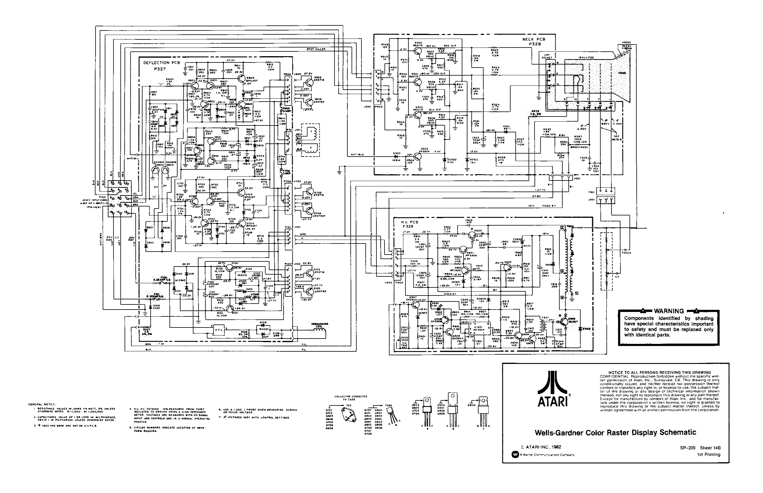
This page is a drawing, shown as the original scan.
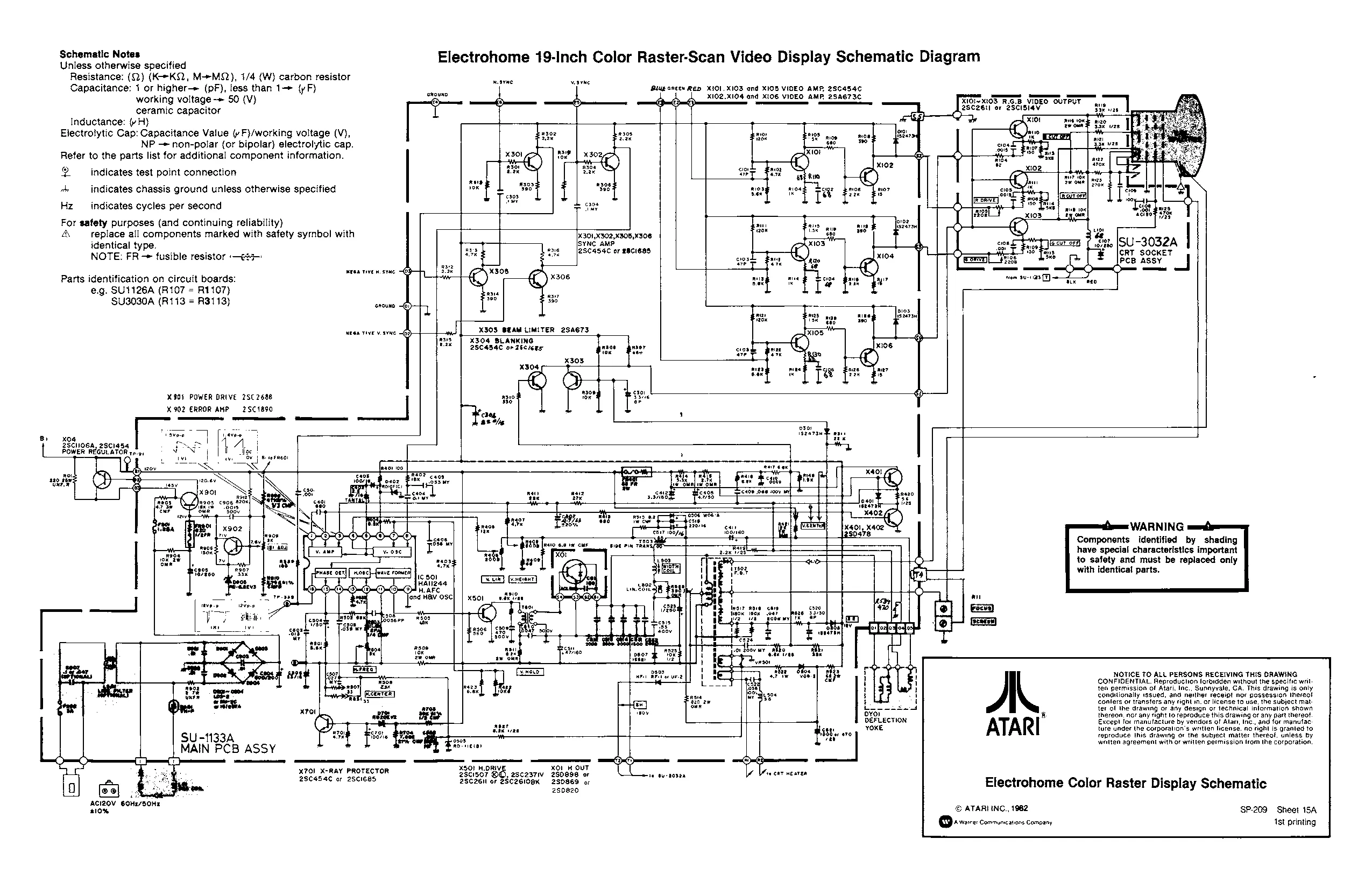
Schematic Notes Electrohome 19-Inch Color Raster-Scan Video Display Schematic Diagram Unless otherwise specified Resistance: (2) (K-*KQ., M*MQ), 1/4 {W) carbon resistor save wearne Capacitance: 1 or higher» (pF), less than 1» {yF} Blue ome RED XIO1, X103 ond XIO5 VIDED AMP, 2564546
| working voltage -» 50 (V) | Na | _4, | | | d | X102.X104 ond X106 VIDEO AMP. 25A673C | met | GSeRIOIE NIDEO OUTFUT. |
ceramic capacitor ~ 2sczei or @Scisiav Inductance: (vH)} Electrolytic Cap: Capacitance Value { F}/working voltage (V}, NP -* non-polar (or bipolar} electrolytic cap. Refer to the parts list for additional component information. Q indicates test point connection ane hy indicates chassis ground unless otherwise specified von Hz indicates cycles per second For safety purposes (and continuing reliability) & replace all components marked with safety syrnbol with x301,X302,X305,X306
| identical type. | one | SYNC AMP |
| NOTE: FR- fusible resistor | TH | [PSoasse or gacieas |
wrea tive nsec CP Parts identification on circuit boards: x306 e.g. SUI126A (R107 = R1107} 7 SU3030A (R113 = R3113) snouno 0) a
NEGA TIVE V.S¥HC —G3> | | t K303 BEAM LIMITER 254673
- X304 BLANKING 2SC434C or 26cieas
X01 POWER DRIVE 25C 2686 Bek X 902 ERROR AMP — 251890 | ee
x04 25C06A, 2801454 Power REGULATOR
420 8 pera cot Bite e408 48 100
noe FW WARNING
ic bathe Components identified by shading
| - | ioe | have special characteristics important | ||
| 3384) | 32°* | | | = | to safety and must be replaced only |
ai with identical parts.
NOTICE TO ALL PERSONS RECEIVING THIS DRAWING CONFIDENTIAL. Reproduction forbidden without the specific writ ten permission of Atari. Inc., Sunnyvale, GA, This drawing is only conditionally wssued, and nerthes receipt nor gassession Ineseot
conlers or transters any rignl in. or license to use, the subject mat
ter of the drawing or any design or technical iniarmation shown
Oyo) a thereon, nor any raght 10 reproduce this Grawing of any part thereot
DEFLECTION Excepl for manufacture by ventiors of Alar, Ine. and for manufac YOKE ture under the corporation's writlen license, no right is granted to feproduce this drawing or the subject matier thereof, unless Dy walten agreement with or writien permission learn the corporation
X70) X-RAY PROTECTOR Heiss? BS, escosrw Bspe98 oF 1 bur soten cer mearen 2SC45AC of 25CI6ES a8Cz0H oF G8CeCIOEK 250868 Electrohome Color Raster Display Schematic
s10% © ATAREING., 1962 SP-209 Sheet 154 QD rere: Commumcations Company 1st printing