Pole Position SP-218 4th Printing
Pole Position (World) (Namco, 1982) · Schematic Package · 32 pages · 84 sections · original scan
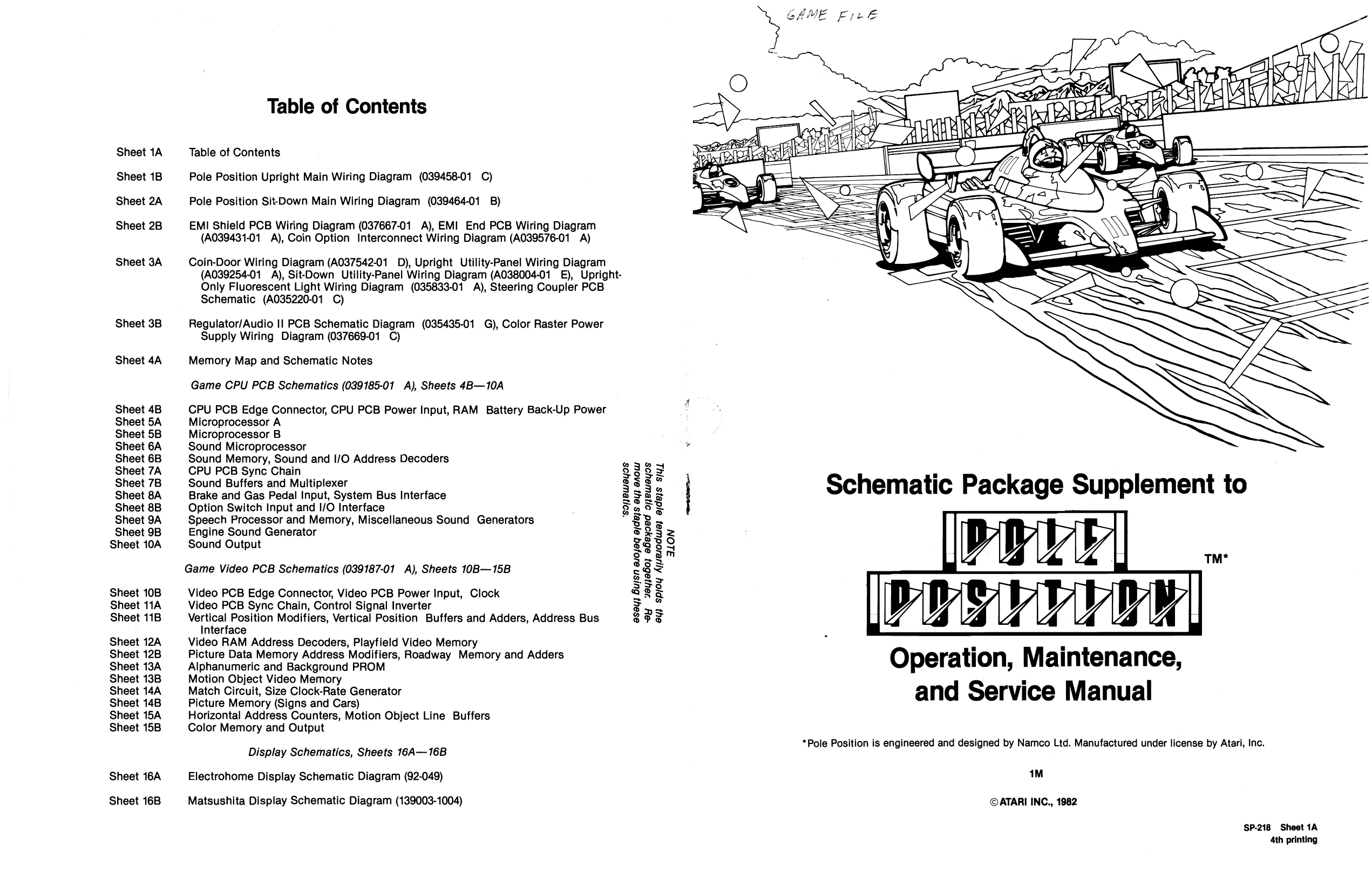
Table of Contents
Sheet 1A Table of Contents
Sheet 1B Pole Position Upright Main Wiring Diagram (039458-01 C)
Sheet 2A Pole Position SitDown Main Wiring Diagram (039464-01 B)
Sheet 2B EMI Shield PCB Wiring Diagram (037667-01 A), EMI End PCB Wiring Diagram (A039431-01 A), Coin Option Interconnect Wiring Diagram (A039576-01 A)
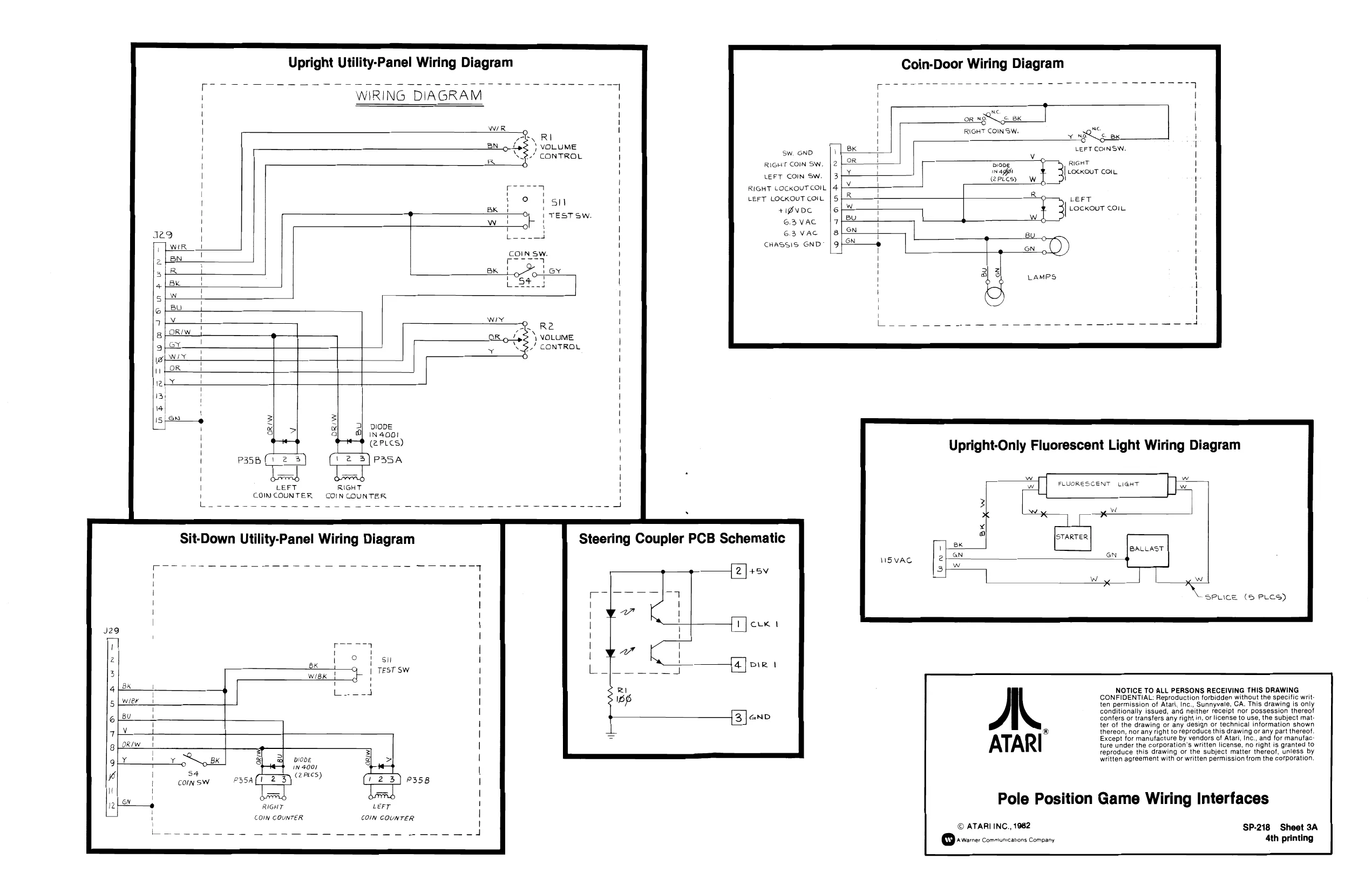
Sheet 3A Coin-Door Wiring Diagram (A037542-01 D), Upright Utility-Panel Wiring Diagram (A039254-01 A), Sit-Down Utility-Panel Wiring Diagram (A038004-01 E), Upright- Only Fluorescent Light Wiring Diagram (035833-01 A), Steering Coupler PCB Schematic (A035220-01 C)
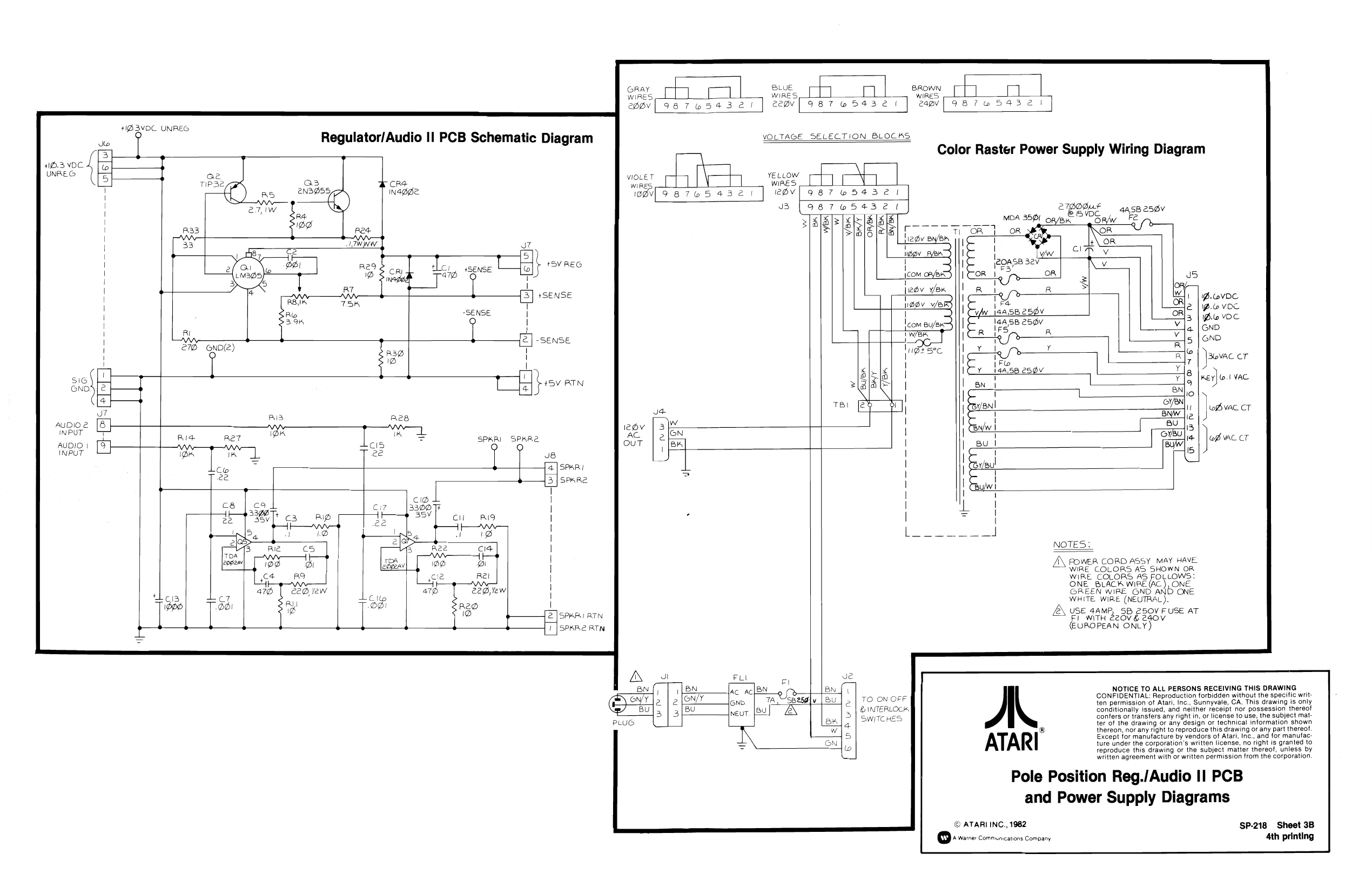
Sheet 3B Regulator/Audio Il PCB Schematic Diagram (035435-01 G), Color Raster Power Supply Wiring Diagram (037669-01 C)
Sheet 4A Memory Map and Schematic Notes
Game CPU PCB Schematics (039185-01 A), Sheets 4B—10A
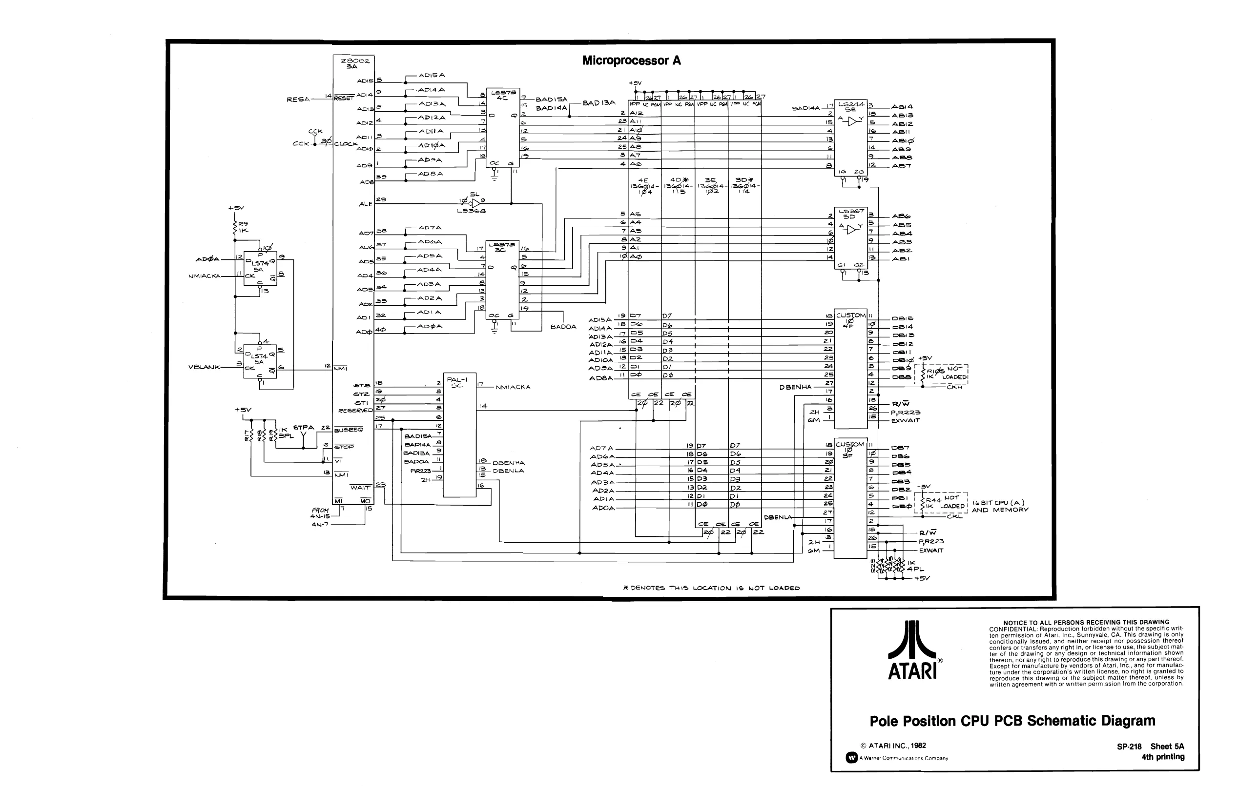
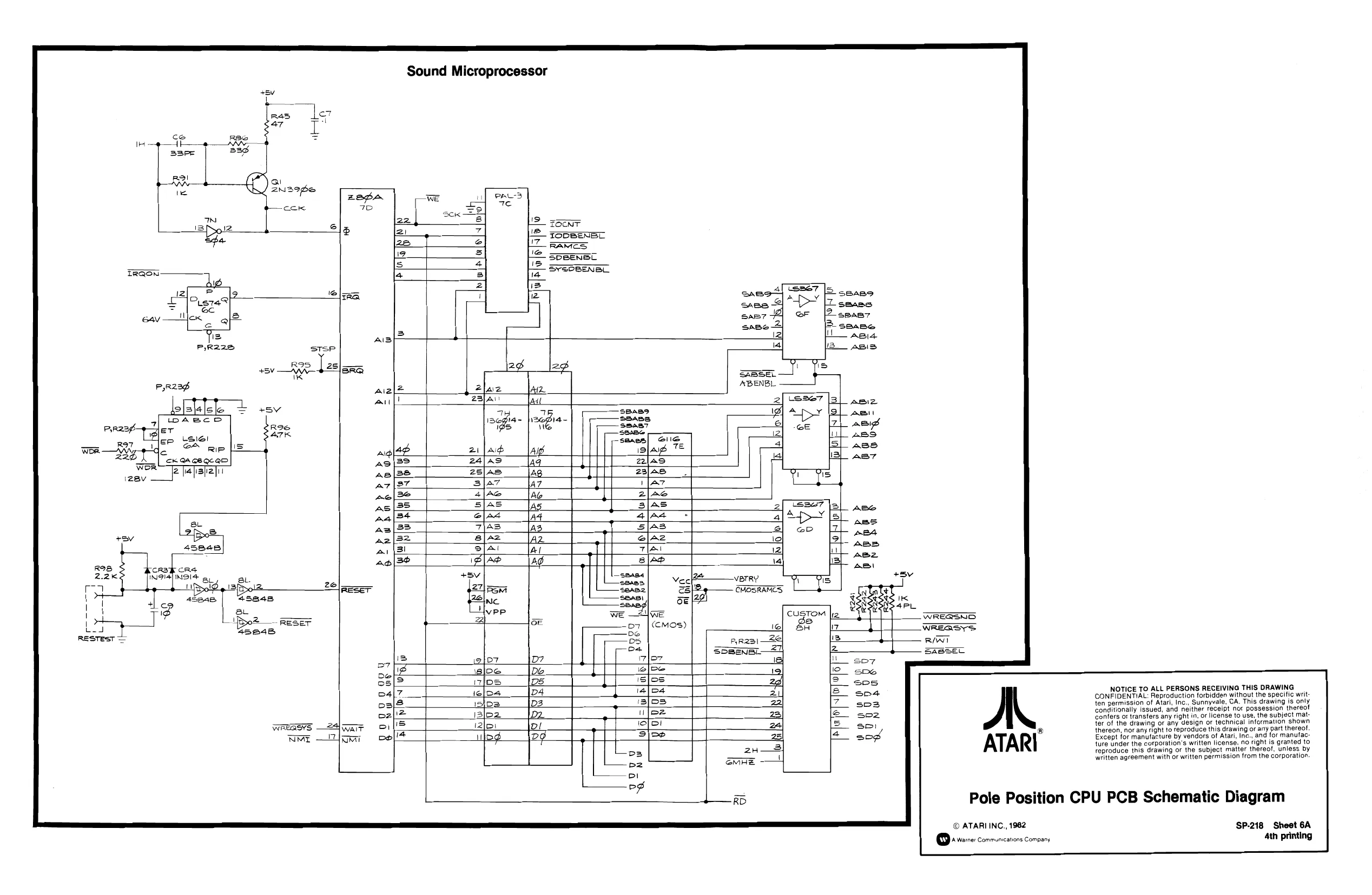
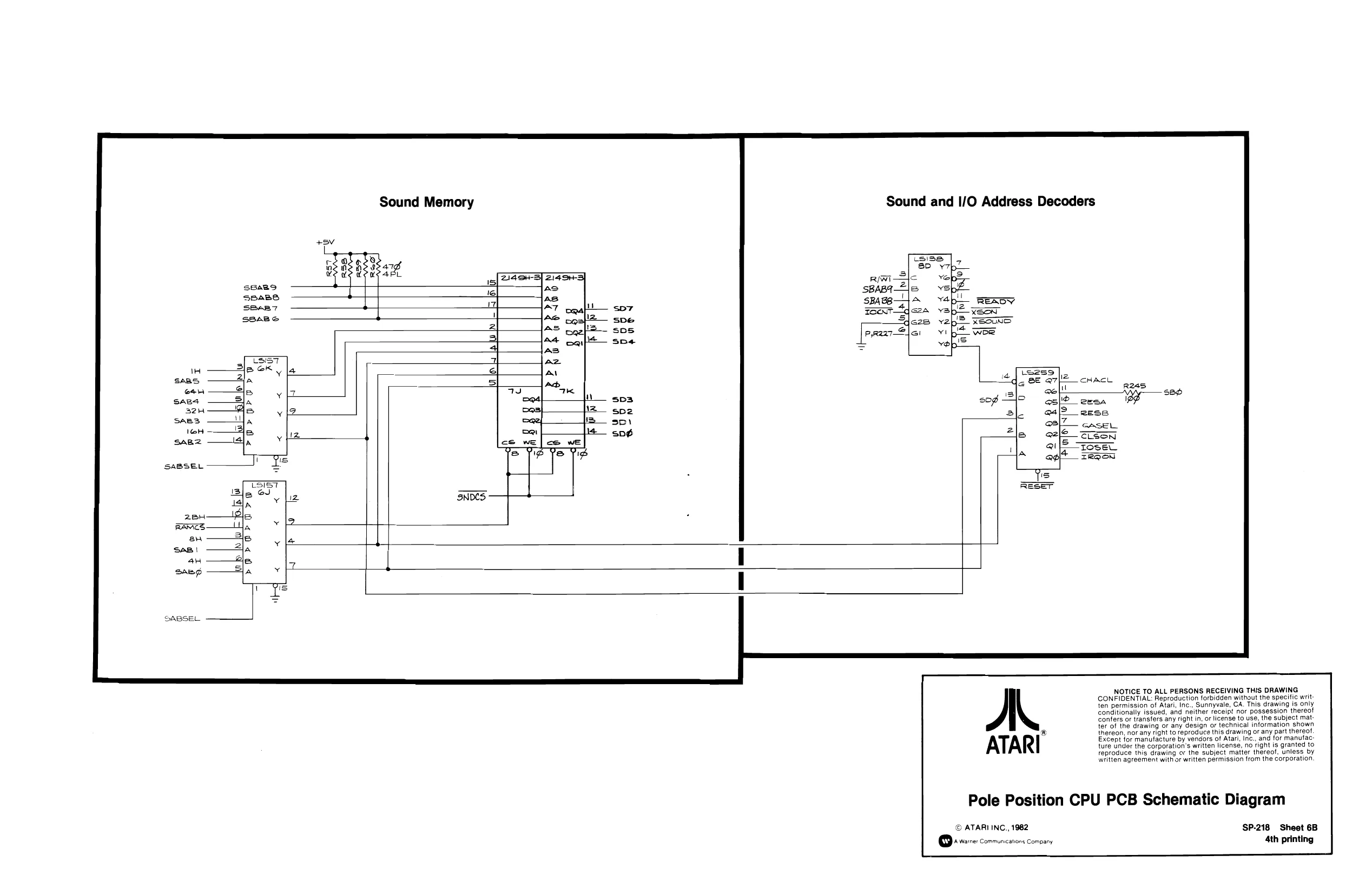
Sheet 4B CPU PCB Edge Connector, CPU PCB Power Input, RAM Battery Back-Up Power Sheet 5A Microprocessor A Sheet 5B Microprocessor B Sheet 6A Sound Microprocessor * Sheet 6B Sound Memory, Sound and I/O Address Decoders Sheet 7A CPU PCB Sync Chain Sheet 7B Sound Buffers and Multiplexer Sheet 8A Brake and Gas Pedal Input, System Bus Interface Sheet 8B Option Switch Input and 1/O Interface Sheet 9A Speech Processor and Memory, Miscellaneous Sound Generators Sheet 9B Engine Sound Generator Sheet 10A Sound Output ‘soeuseyos asey) Bujsn aojaq ajde}s ay} aAow
ALON TM* Game Video PCB Schematics (039187-01 A), Sheets 10B—15B
Sheet 10B Video PCB Edge Connector, Video PCB Power Input, Clock Sheet 11A Video PCB Sync Chain, Control Signal Inverter Sheet 11B Vertical Position Modifiers, Vertical Position Buffers and Adders, Address Bus -9y 4ayjebo} abeyoed oneweyos ey) spjoy Ajjesodwe} ajdeys siy1
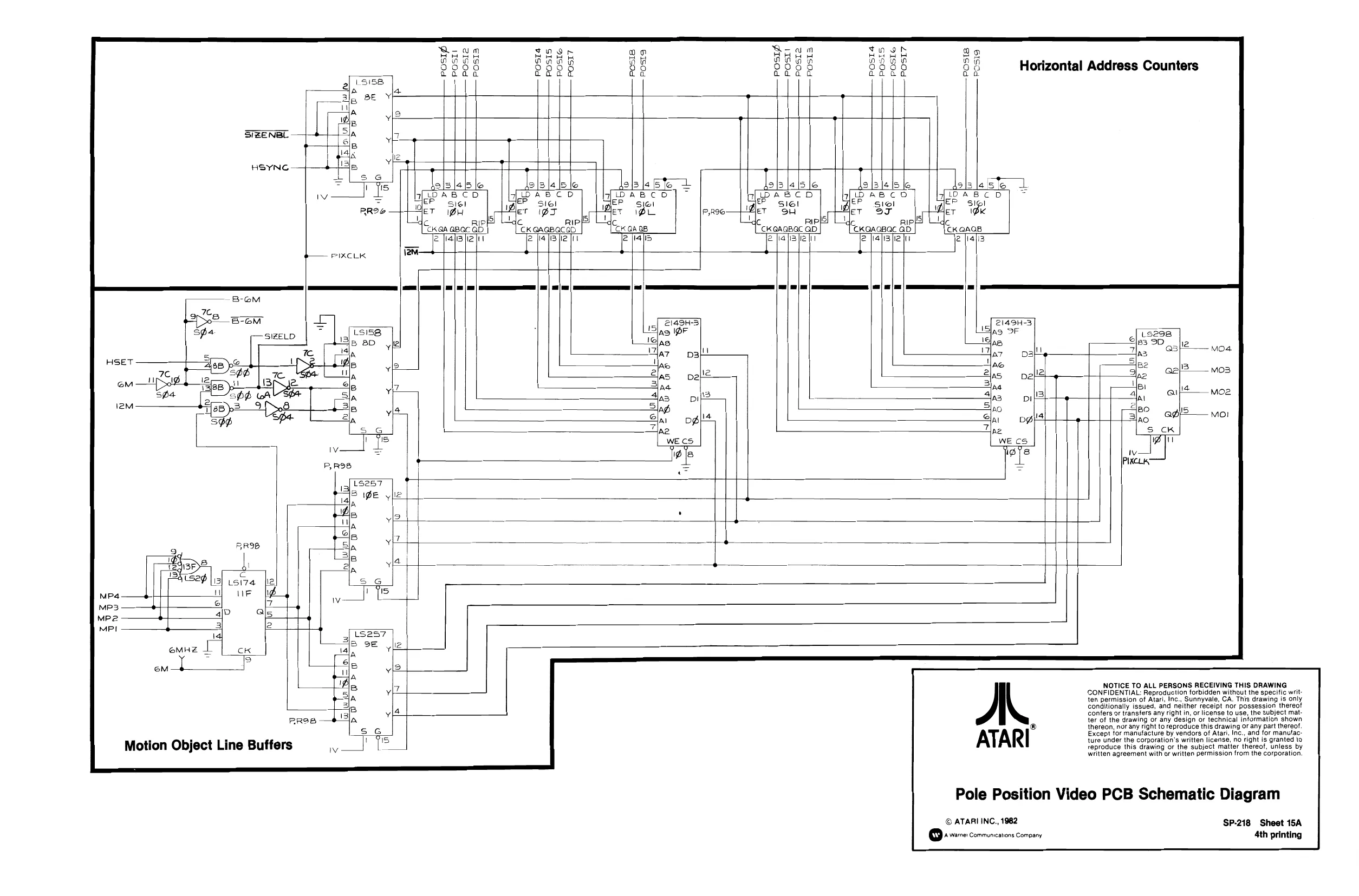
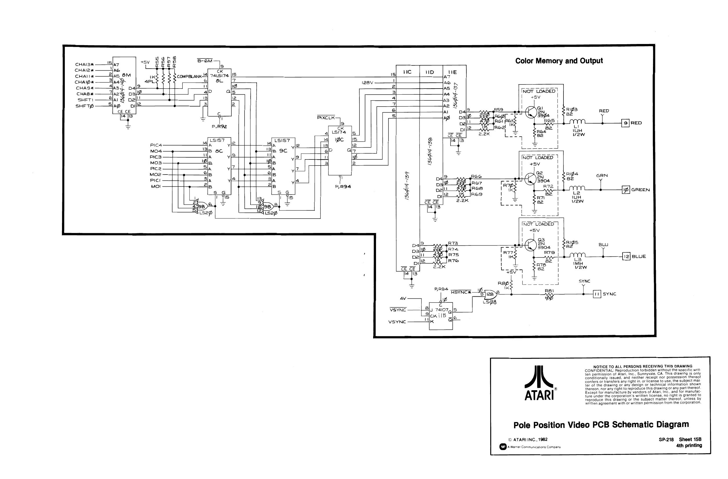
Interface Sheet 12A Video RAM Address Decoders, Playfield Video Memory . . 1. Sheet 12B Picture Data Memory Address Modifiers, Roadway Memory and Adders Sheet 13A Alphanumeric and Background PROM Y y Operation, Maintenance, Sheet 13B Motion Object Video Memory Sheet 14A Match Circuit, Size Clock-Rate Generator and Service Manual Sheet 14B Picture Memory (Signs and Cars) Sheet 154 Horizontal Address Counters, Motion Object Line Buffers Sheet 15B Color Memory and Output . . *Pole Position is engineered and designed by Namco Ltd. Manufactured under license by Atari, Inc. Display Schematics, Sheets 16A—16B
Sheet 16A Electrohome Display Schematic Diagram (92-049) 1M
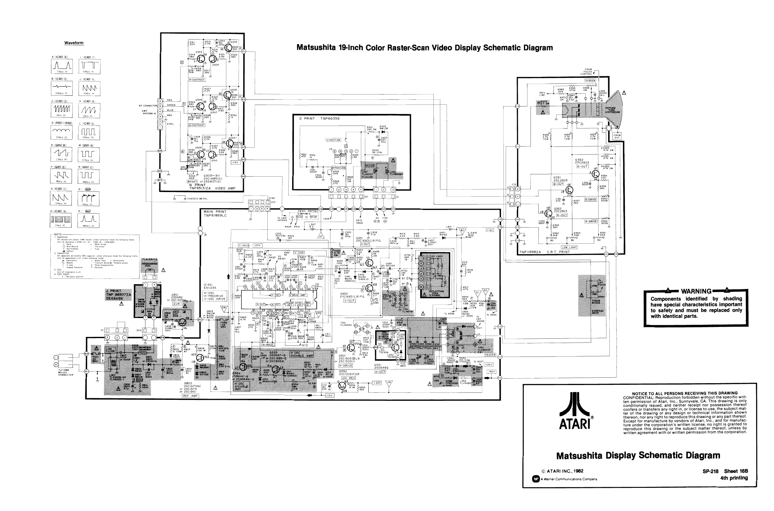
Sheet 16B Matsushita Display Schematic Diagram (139003-1004) ©ATARI INC., 1982
SP-218 Sheet 1A
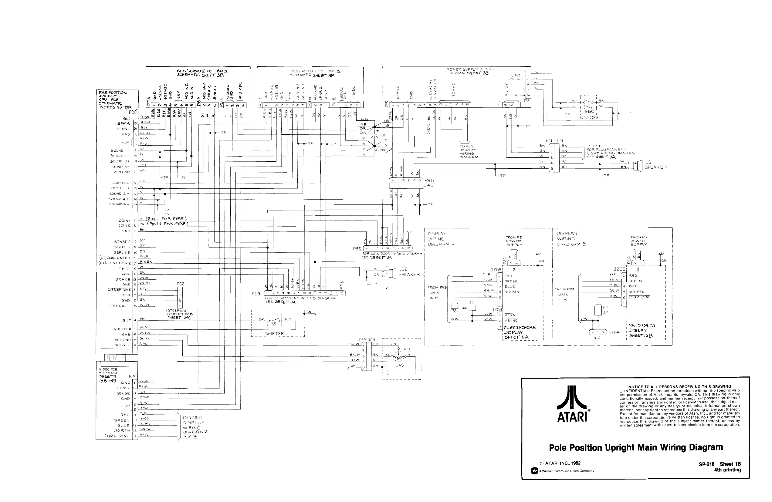
This page is a drawing, shown as the original scan.
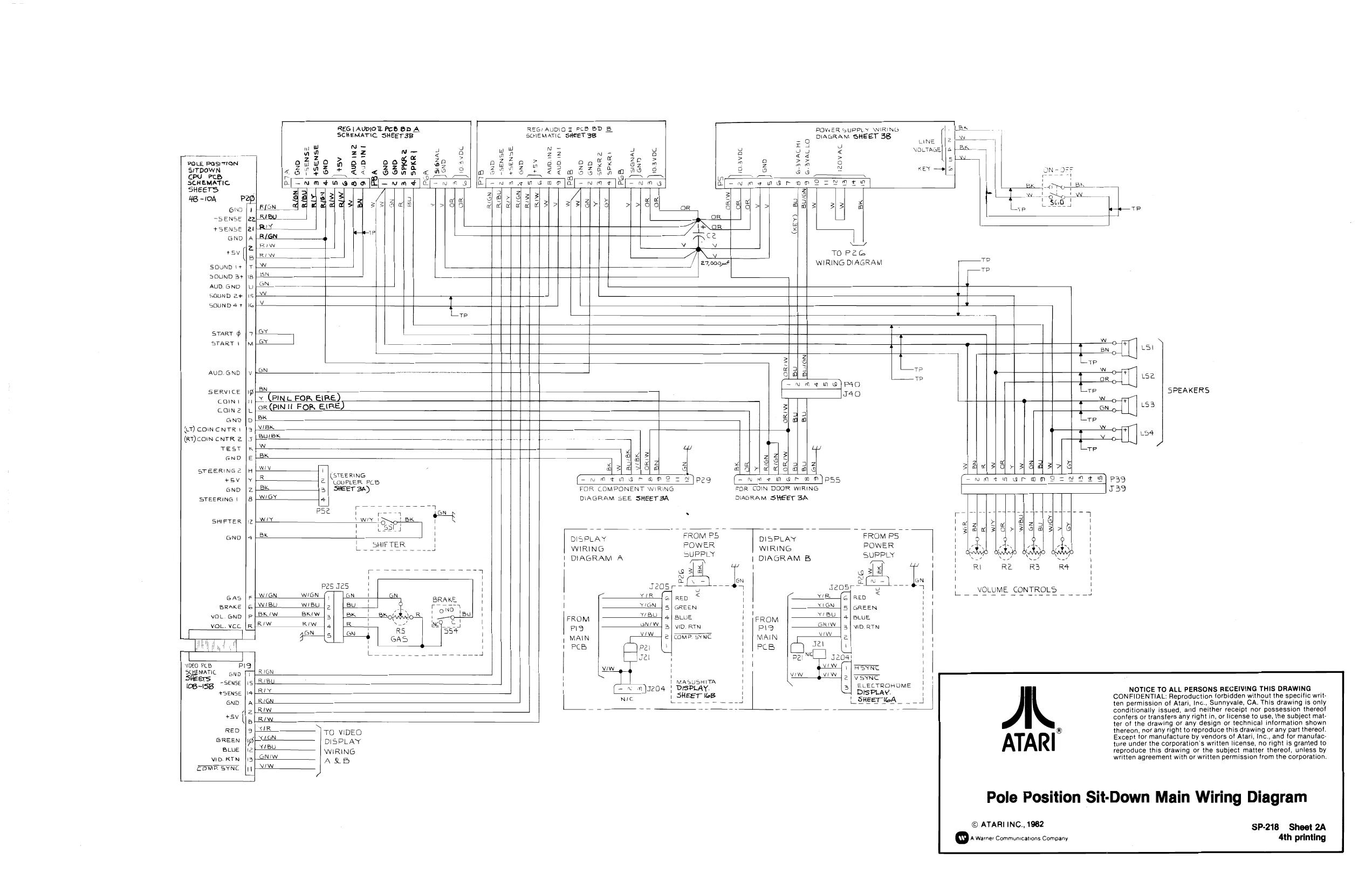
This page is a drawing, shown as the original scan.
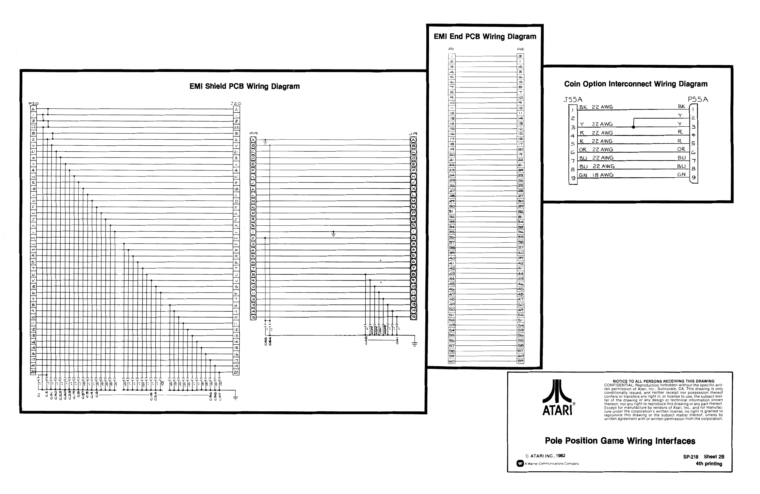
This page is a drawing, shown as the original scan.
This page is a drawing, shown as the original scan.
This page is a drawing, shown as the original scan.
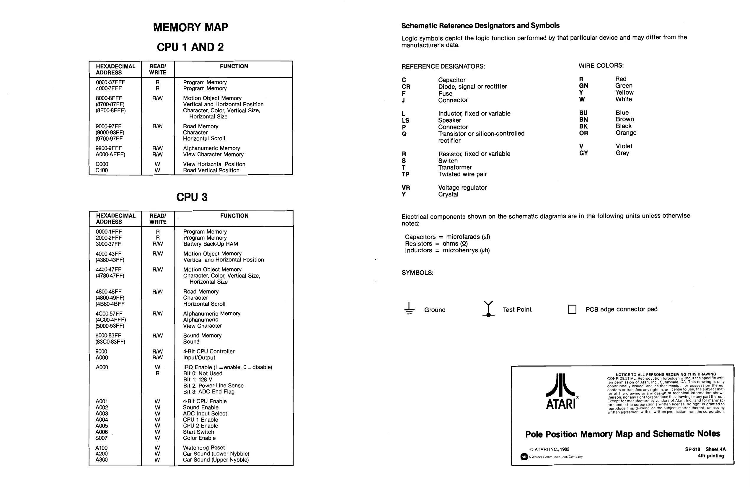
MEMORY MAP
CPU 1 AND 2
HEXADECIMAL READ/ FUNCTION ADDRESS WRITE
R R
0000-37FFF Program Memory
4000-7FFF Program Memory
8000-8FFF (8700-87FF) (8F00-8FFF)
RW Motion Object Memory
Vertical and Horizontal Position
Character, Color, Vertical Size,
Horizontal Size
9000-97FF Road Memory (9700-97FF Horizontal Scroll 9800-9FFF Alphanumeric Memory
(9000-93FF) Character
A000-AFFF) View Character Memory ooo View Horizontal Position C100 Road Vertical Position
CPU 3
0000-1FFF Program Memory 2000-2FFF Program Memory 3000-37FF Battery Back-Up RAM 4000-43FF Motion Object Memory (4380-43FF) Vertical and Horizontal Position 4400-47FF Motion Object Memory (4780-47FF) Character, Color, Vertical Size, Horizontal Size 4800-48FF Road Memory (4800-49FF) Character (4B80-4BFF Horizontal Scroll 4C00-57FF Alphanumeric Memory (4C00-4FFF) Alphanumeric (6000-53FF) View Character 8000-83FF Sound Memory (83C0-83FF) Sound 9000 4-Bit CPU Controller A000 Input/Output IRQ Enable (1 = enable, 0 = disable) Bit 0: Not Used Bit 1: 128 V Bit 2: Power-Line Sense Bit 3: ADC End Flag 4-Bit CPU Enable Sound Enable ADC Input Select CPU 1 Enable CPU 2 Enable Start Switch Color Enable Watchdog Reset Car Sound (Lower Nybble) Car Sound (Upper Nybble) SSS SSSSSSE Schematic Reference Designators and Symbols Logic symbols depict the logic function performed by that particular device and may differ from the manufacturer's data.
REFERENCE DESIGNATORS: WIRE COLORS:
| c | Capacitor | R | Red |
| CR | Diode, signal or rectifier | GN | Green |
| F | Fuse | Y | Yellow |
| J | Connector | Ww | White |
| L | Inductor, fixed or variable | BU | Blue |
| Ls | Speaker | BN | Brown |
| P | Connector | BK | Black |
| Q | Transistor or silicon-controlled | OR | Orange |
rectifier Vv Violet
| R | Resistor, fixed or variable | GY | Gray |
Ss Switch T Transformer TP Twisted wire pair
Voltage regulator Crystal << oo)
Electrical components shown on the schematic diagrams are in the following units unless otherwise noted:
Capacitors = microfarads (uf) Resistors = ohms (2) Inductors = microhenrys (uh)
SYMBOLS:
Lt Ground Test Point Oo PCB edge connector pad
NOTICE TO ALL PERSONS RECEIVING THIS DRAWING CONFIDENTIAL: Reproduction forbidden without the specific written permission of Atari, Inc., Sunnyvale, CA. This drawing is only conditionally issued, and neither receipt nor possession thereot confers or transfers any right in, or license to use, the subject mat: ter of the drawing ot any design or technical information shown ® thereon, nor any right to reproduce this drawing or any part thereof, Except for manufacture by vendors of Atari, Inc., and for manufacture under the corporation’s written license, no right is granted to reproduce this drawing or the subject matter thereof, unless by written agreement with or written permission from the corporation.
Pole Position Memory Map and Schematic Notes
© ATARI INC., 1982 SP-218 Sheet 4A > ware: Communications Company 4th printing
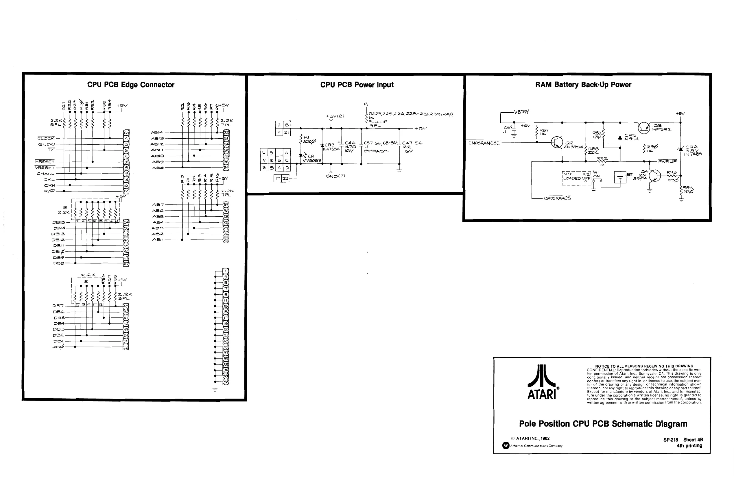
CPU PCB Edge Connector CPU PCB Power Input RAM Battery Back-Up Power
‘ A
+5v(2) $223,225 226,228-23,239,240 PULLUP, QPL +5V
(S7-66,68-4L 647-56 D 22, BYrAse |* sso 22K
R22.
Me
Wot wal WI
Not wal WI LOADED OFF a IHHOSNOOSS S
Confers or transfers any right in, or license to use, the subject mat
ter of the drawing or any design of technical iniormation shown
® thereon, nor any right to reproduce this drawing or any part thereof
Except for manufacture by vendors of Atari, Inc., and tor manutac: ture under the corporation's written license, no right 1s granted to reproduce this drawing or the subject matter thereof, unless oy written agreement with or written permission from the corporation NOTICE TO ALL PERSONS RECEIVING THIS DRAWING CONFIDENTIAL: Reproduction forbidden without the specific writ: ten permission of Atari, Inc., Sunnyvale, CA. This drawing is only conditionally issued, and neither receipt nor possession thereof
Pole Position CPU PCB Schematic Diagram
© ATARI INC. 1982 SP-218 Sheet 4B + Warre: Communications Company 4th printing
This page is a drawing, shown as the original scan.
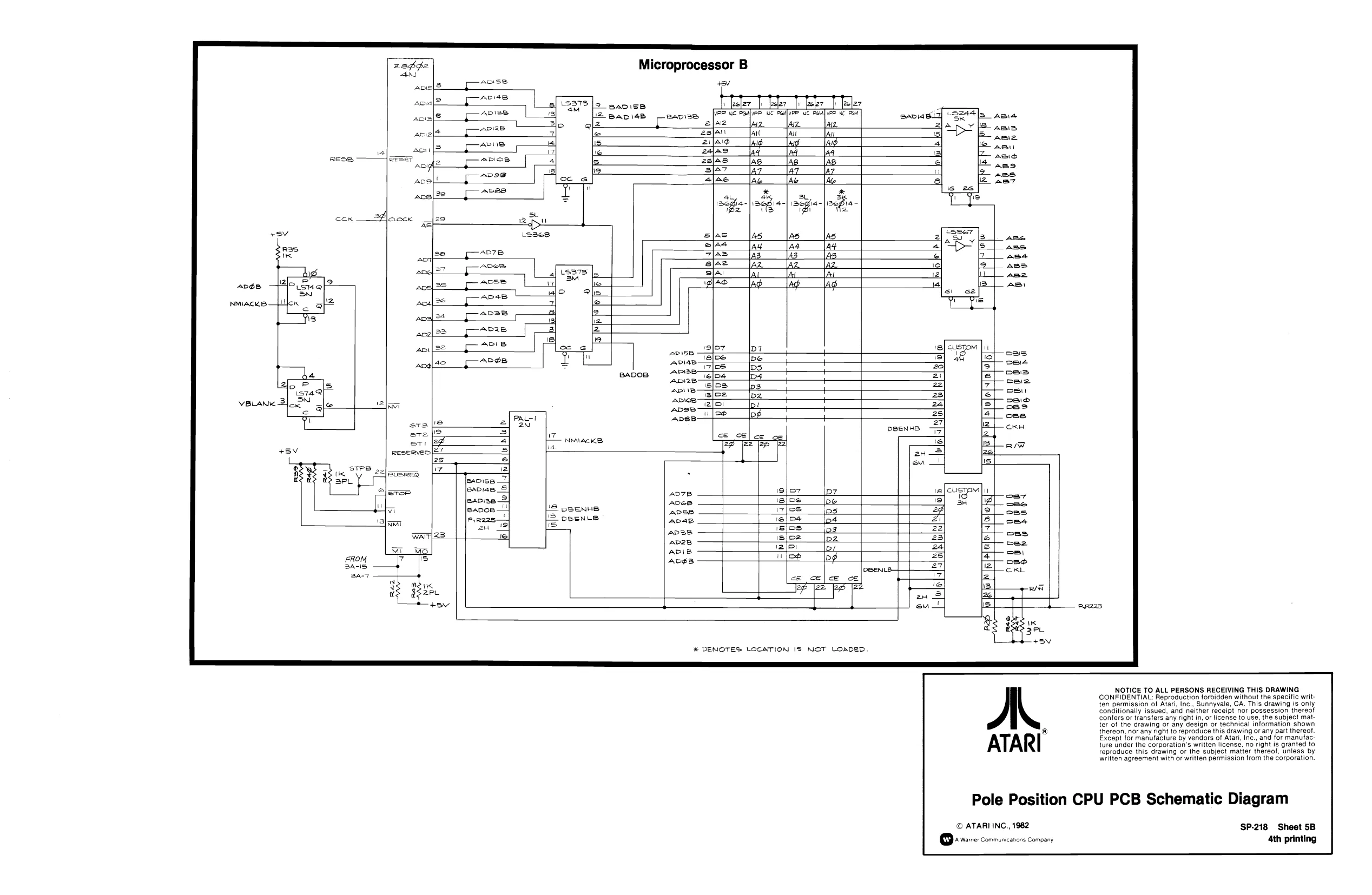
Microprocessor B
pose av
| Acie | Hee | Ee | pee |
4 2 Bavise 1 feoler |i fecler 7 |) feler Apia. 2 BADIAB _waprae [PP NE PRIS UC PANIPE uC PaUp ee AC Pat
| a | none | i | z[ae | la |
| = | 23/an | faut | Al | mn |
| 5 | ACS | Ziad | lad | oa |
| je | zalas | hag |
25/45 3/7 alae
4u, eg iz
a0é8
NMIACKB.
CUSTOM 7S] 4
25] Zt 22]
2A] 25) sT3 27, st2 DBENHB ——
str 12) RESERVED! 24 = ow
BUSREQ
cusTam i 3H DBENHS DBENLS Re ® SOO opOS.
we
% DENOTES LOCATION IS NOT LOADED
NOTICE TO ALL PERSONS RECEIVING THIS DRAWING CONFIDENTIAL: Reproduction forbidden without the specific writ ten permission of Atari, Inc., Sunnyvale, CA. This drawing is only conditionally issued, and neither receipt nor possession thereof! Confers or transfers any right in, or license to use, the subject mat. ter of the drawing or any design or technical information shown
thereon, nor any right to reproduce this drawing or any part thereof!
Except for manufacture by vendors of Atari, Inc., and for manufac: ture under the corporation's written license, no right is granted to reproduce this drawing or the subject matter thereof, unless by written agreement with or written permission from the corporation.
Pole Position CPU PCB Schematic Diagram
© ATARI INC., 1982 SP-218 Sheet 5B tw) ‘A Warner Communcations Company 4th printing
This page is a drawing, shown as the original scan.
This page is a drawing, shown as the original scan.
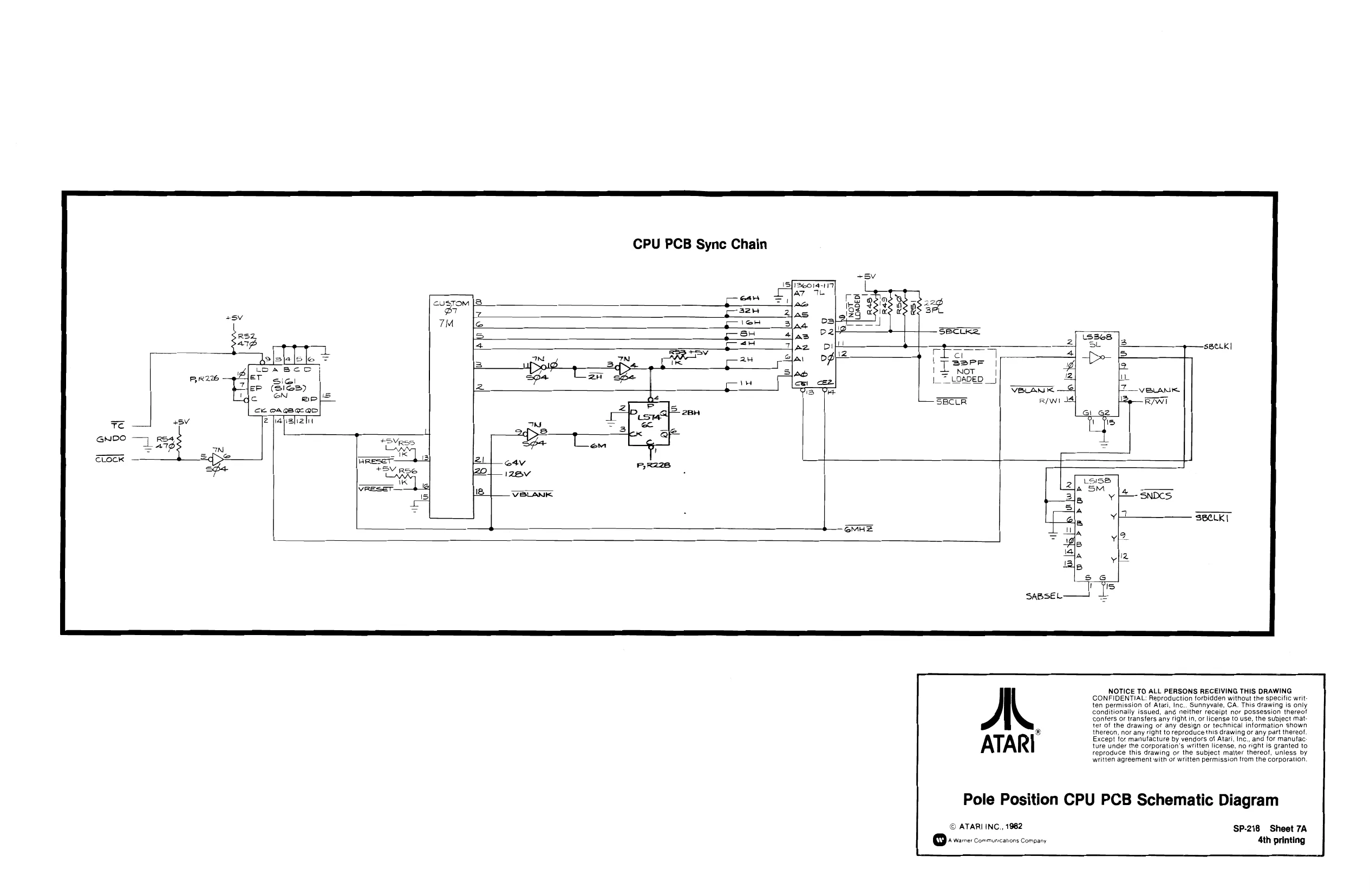
This page is a drawing, shown as the original scan.
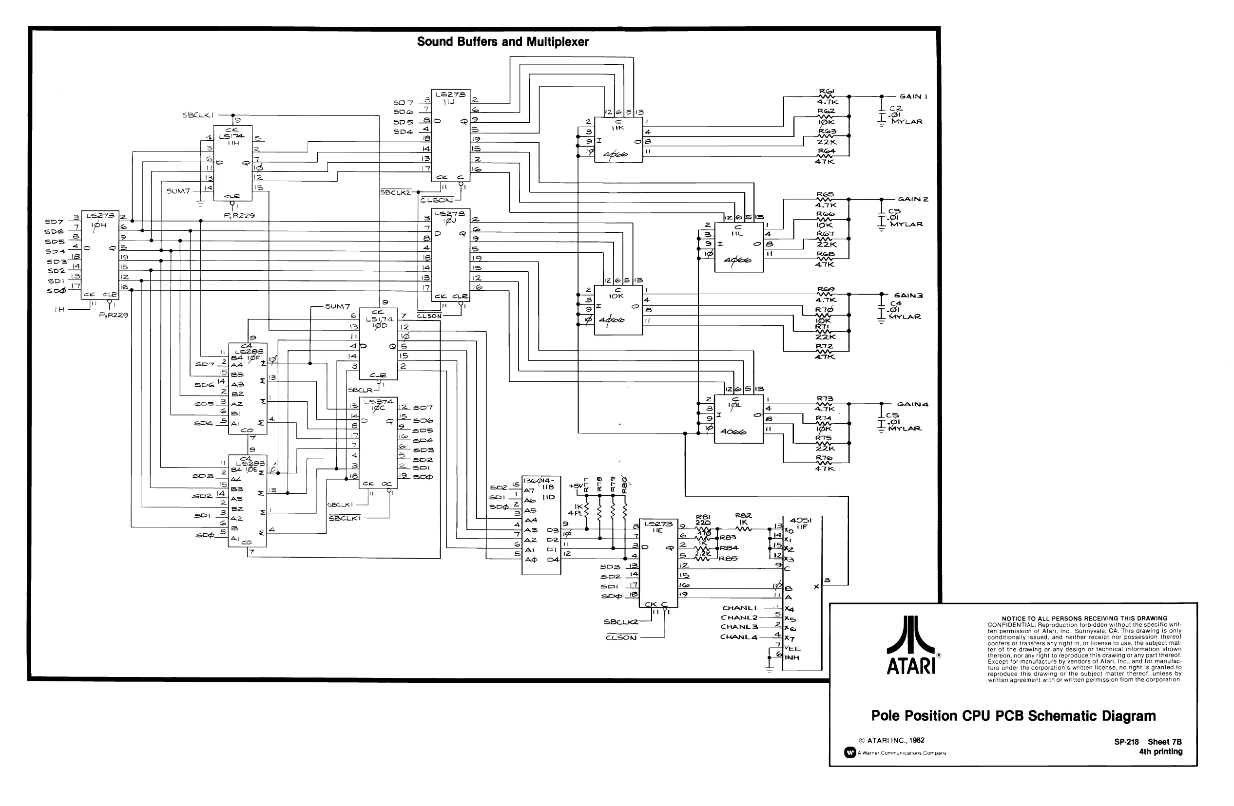
SBCLKI fe
sims
Sound Buffers and Multiplexer
3| thet
oe
SUM7 a Ke
[SBCLRZ—-p—— iv a ccSon
us2738 ips
i=} Q
G6AIN2 ca T&use
+ GaIna
cS “BI Tian
CHANLI
CHANL2 CHANLA.
CHANL 4
NOTICE TO ALL PERSONS RECEIVING THIS DRAWING CONFIDENTIAL: Reproduction forbidden without the specific writ: ten permission of Atari, Inc., Sunnyvale, CA. This drawing is only conditionally issued, and neither receipt nor possession thereot confers or transfers any right in, or license to use, the subject mat. ter of the drawing or any design or technical information shown ® thereon, nor any right to reproduce this drawing or any part thereof. Except for manufacture by vendors of Atari, Inc., and for manufac: ture under the corporation's written license, no right is granted to reproduce this drawing or the subject matter thereof, unless by written agreement with or written permission from the corporation.
Pole Position CPU PCB Schematic Diagram
© ATARI INC., 1982 SP-218 Sheet 7B fw Warner Communications Company 4th printing
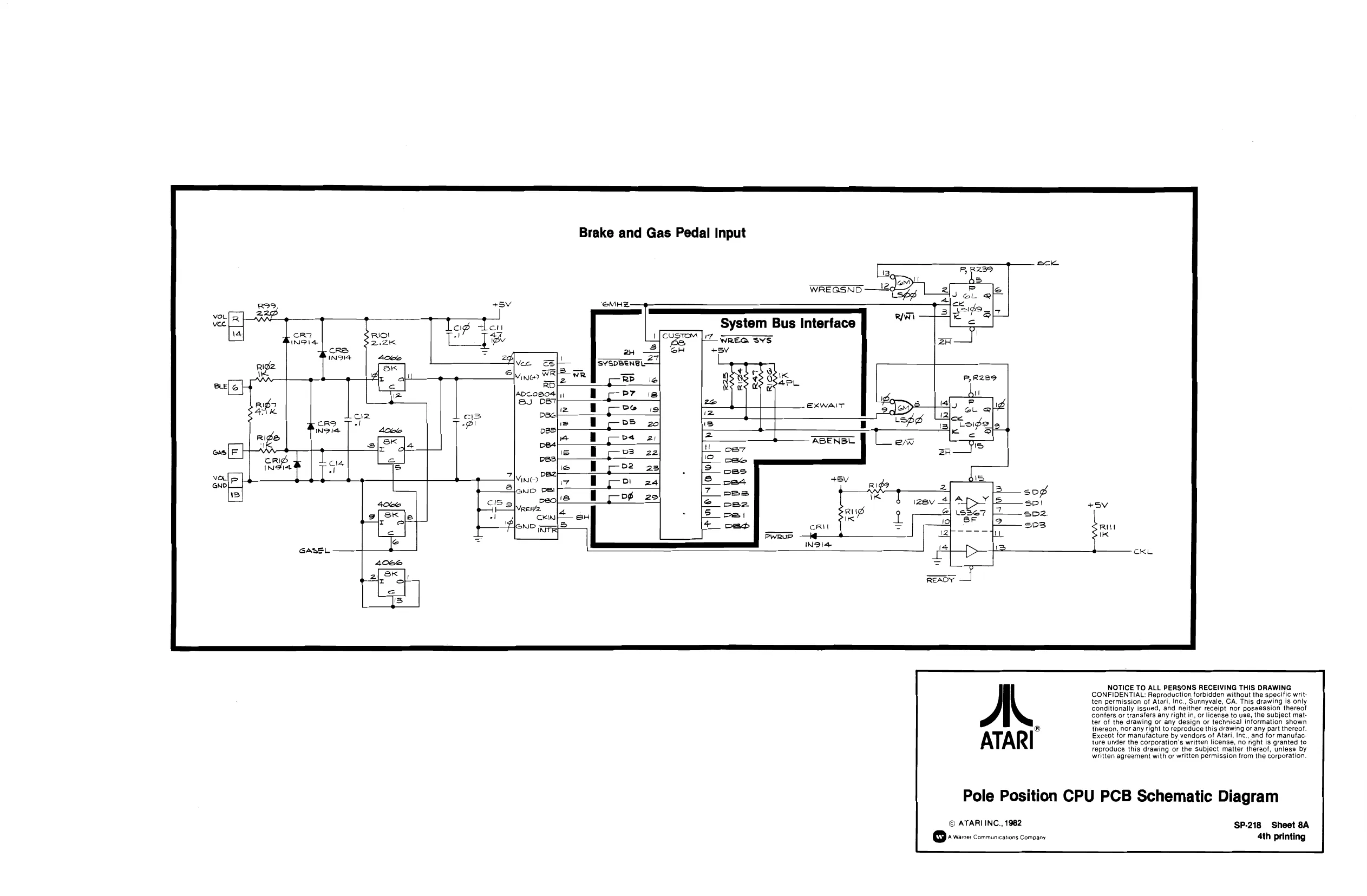
Brake and Gas Pedal Input
WREGSND
System Bus Interface
I aa 17 }+— WREG SYS a | ev ae 27 SYSDBENEL- Mec, ES Mineo WR RB RP ie lAncogo4} is BU 087
Dec! ‘9|
pes]
pes]
pes 20]
2!
23]
Confers or transfers any right in, or license to use, the subject mat- NOTICE TO ALL PERSONS RECEIVING THIS DRAWING CONFIDENTIAL: Reproduction forbidden without the specific written permission of Atari, Inc., Sunnyvale, CA. This drawing is only Conditionally issued, and neither receipt nor possession thereot
ter of the drawing or any design or technical information shown ® thereon, nor any right to reproduce this drawing or any part thereof. Except for manufacture by vendors of Atari, Inc., and for manufac: ture under the corporation's written license, no right Is granted to reproduce this drawing or the subject matter thereof, unless by written agreement with or written permission from the corporation.
Pole Position CPU PCB Schematic Diagram
© ATARI INC., 1982 SP-218 Sheet 8A
fw Warner Communications Company 4th printing
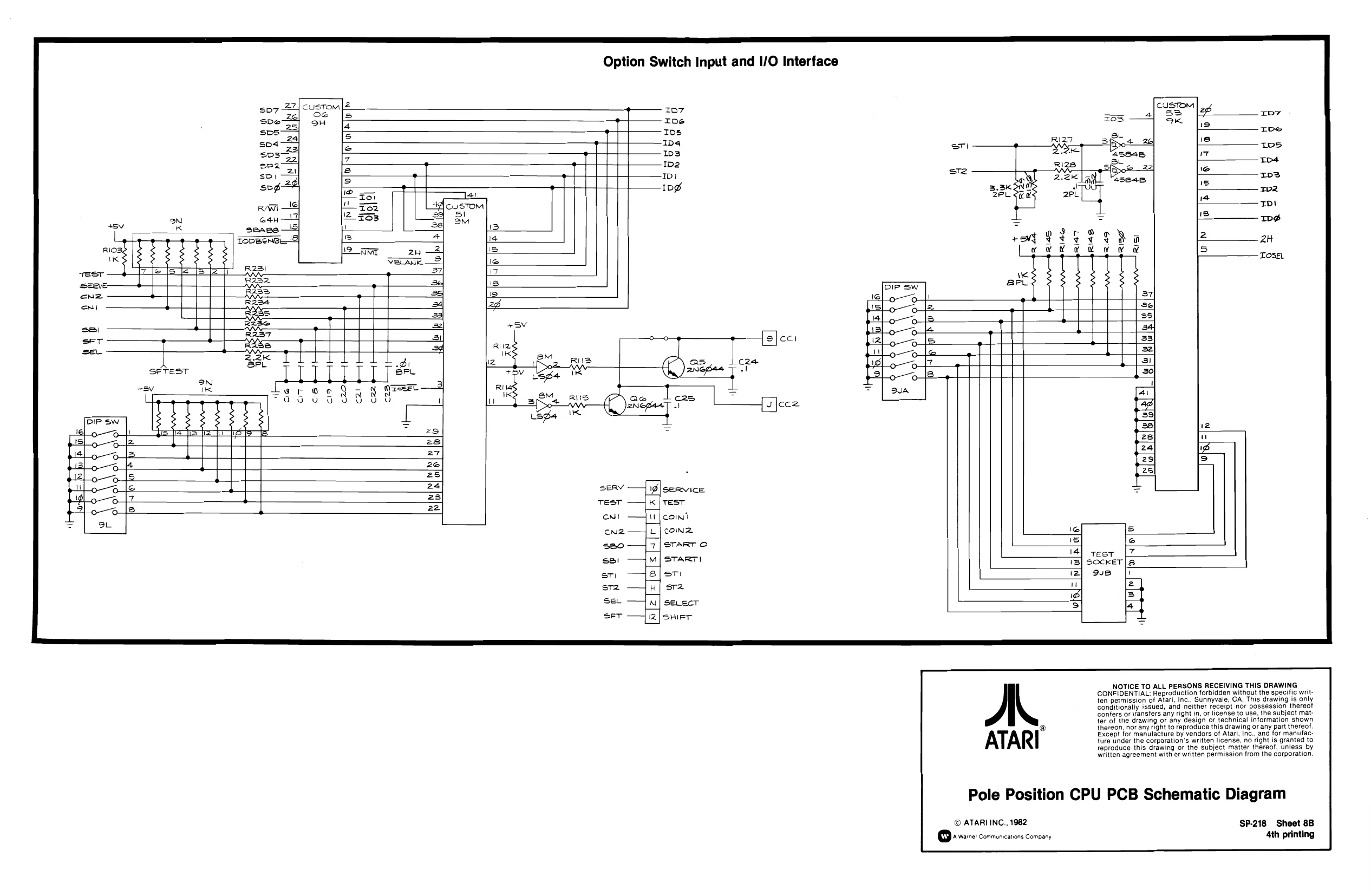
Option Switch Input and |/O Interface
custom Oe OH ros
eu 34 24 4sec5 su 2a Laat Oece OU 2PL SDI sop
rem S| oan senes Topeens._/4 BH) 0) O 1H] W/Ajy [ys
a © Eq
x I 1p Jf Fs ee Ue 1 foo > | 81
R231
Resz,
Res
Rasa
RSS Rese
R237
eS
2.2K [ elelelelelalgle
ES
‘
SERVICE
Test a)
COIN’
cOINZ,
START O
START!
oT
rz
SELECT F]W)%] -]o]xJo
SHIFT
confers or wransfers any right in, or license to use, the subject mat: ter of the drawing or any design or technical information shown
3) thereon, nor any right to reproduce this drawing or any part thereof,
Except for manutacture by vendors of Atari, Inc., and for manufac: ture under the corporation's written license, no right is granted to reproduce this drawing or the subject matter thereof, unless by written agreement with or written permission from the corporation. NOTICE TO ALL PERSONS RECEIVING THIS DRAWING CONFIDENTIAL: Reproduction forbidden without the specific written permission of Atari, Inc., Sunnyvale, CA. This drawing is only conditionally issued, and neither receipt nor possession thereof
®
Pole Position CPU PCB Schematic Diagram
ATARI INC., 1982 SP-218 Sheet 8B + Warrer communications Comoany 4th printing
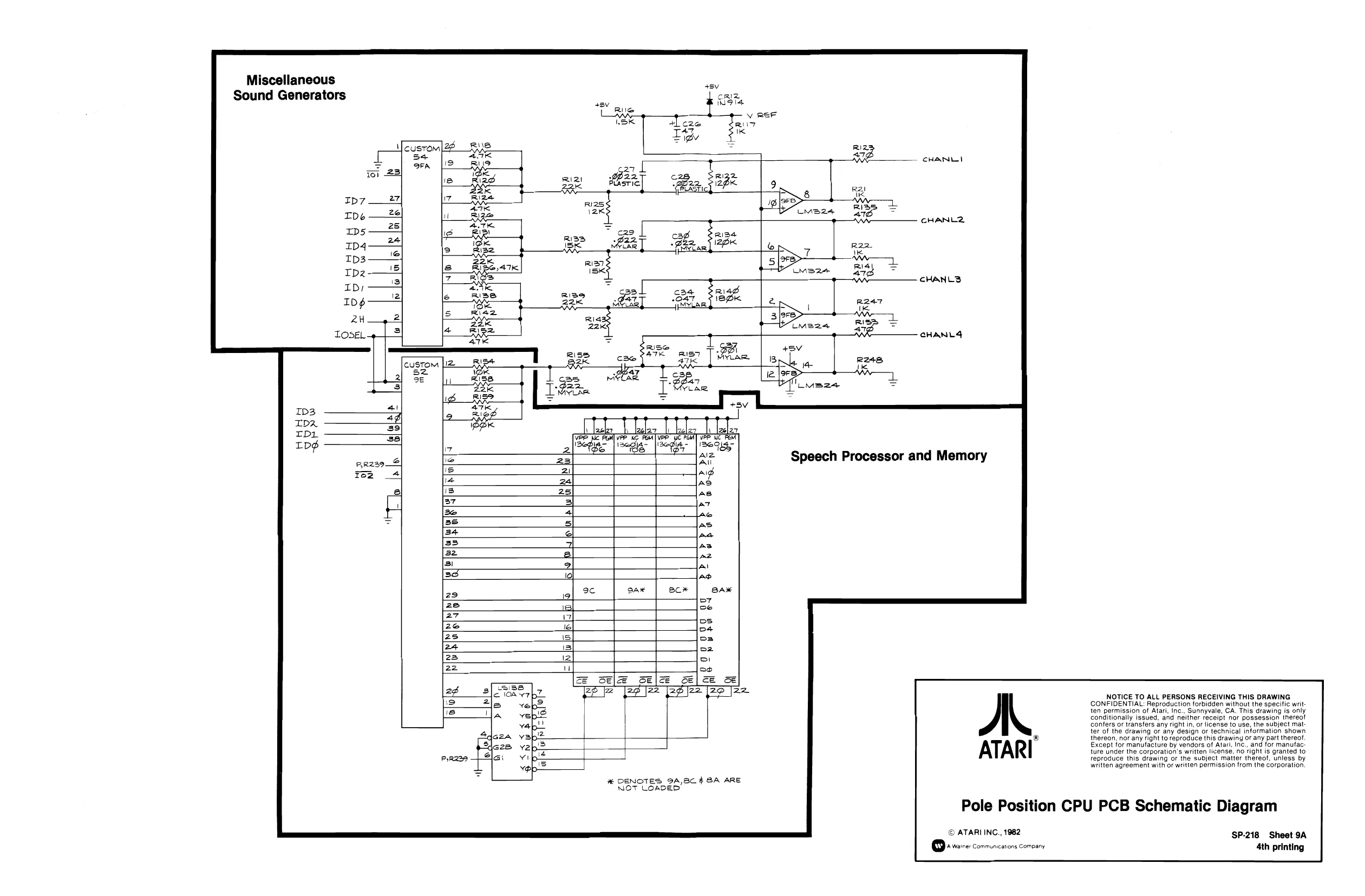
Miscellaneous Sound Generators
cusTOmM CHANLI
custom Sz 3E
ny IS O_O fy [or fora fw fur
2s 9c go
i
% DENOTES 9A,8c 4 8A ARE NOT LOADED’
Speech Processor and Memory
AL ATARI NOTICE TO ALL PERSONS RECEIVING THIS DRAWING CONFIDENTIAL: Reproduction forbidden without the specitic writ
ten permission of Atari, Inc., Sunnyvale, CA. This drawing is only
Conditionally issued, and neither receipt nor possession thereof
confers or transfers any right in, or license to use, the subject mat thereon, nor any right to reproduce this drawing or any part thereof written agreement with or written permission from the corporation
ter of the drawing or any design or technical information shown thereon, nor any right to reproduce this drawing or any part thereof. Except for manufacture by vendors of Ata, Inc., and for manufac: ture under the corporation's written license, no right is granted to reproduce this drawing or the subject matter thereof, unless by written agreement with or written permission from the corporation.
Pole Position CPU PCB Schematic Diagram
© ATARI INC., 1982 SP-218 Sheet 9A
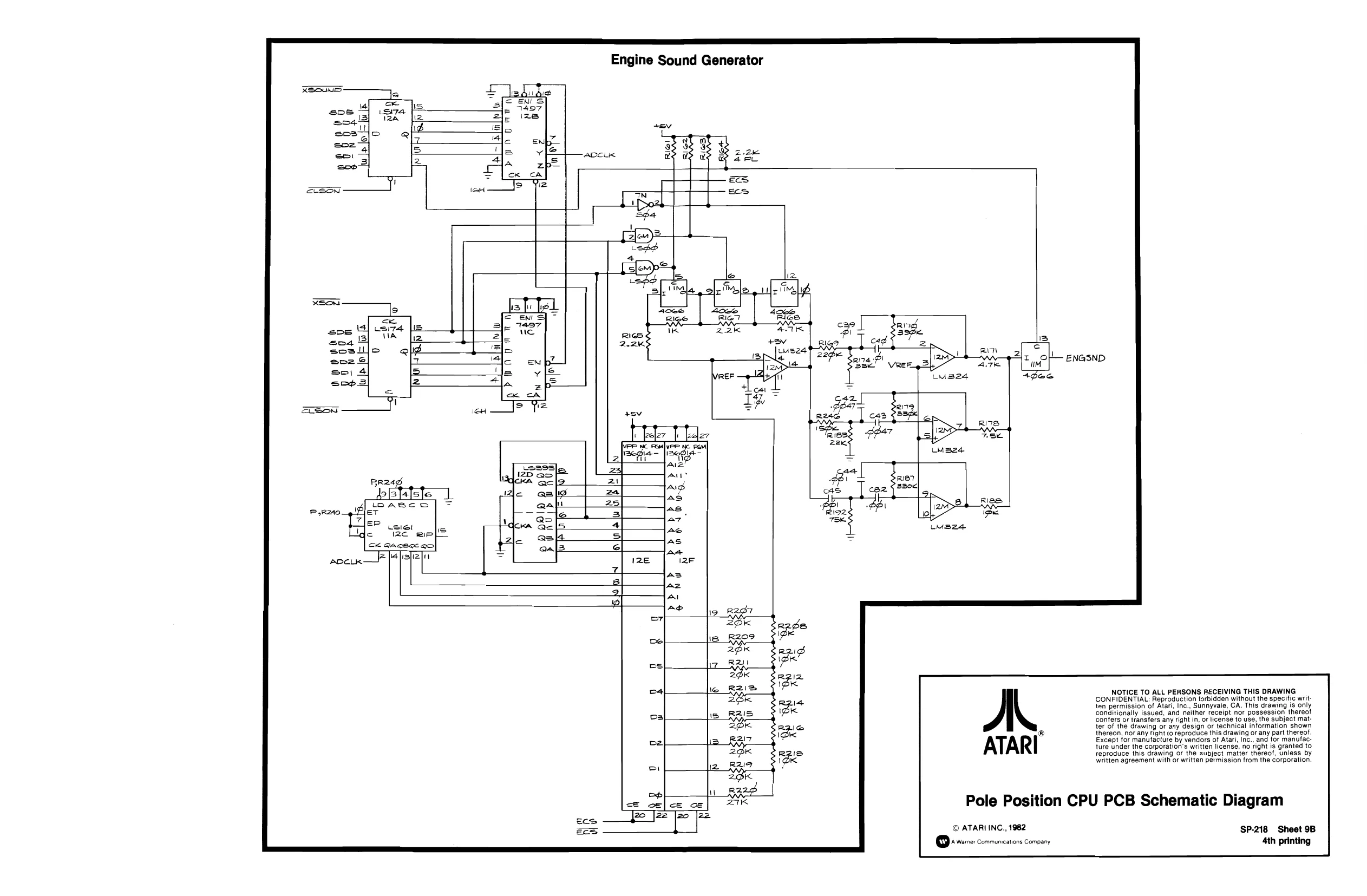
This page is a drawing, shown as the original scan.
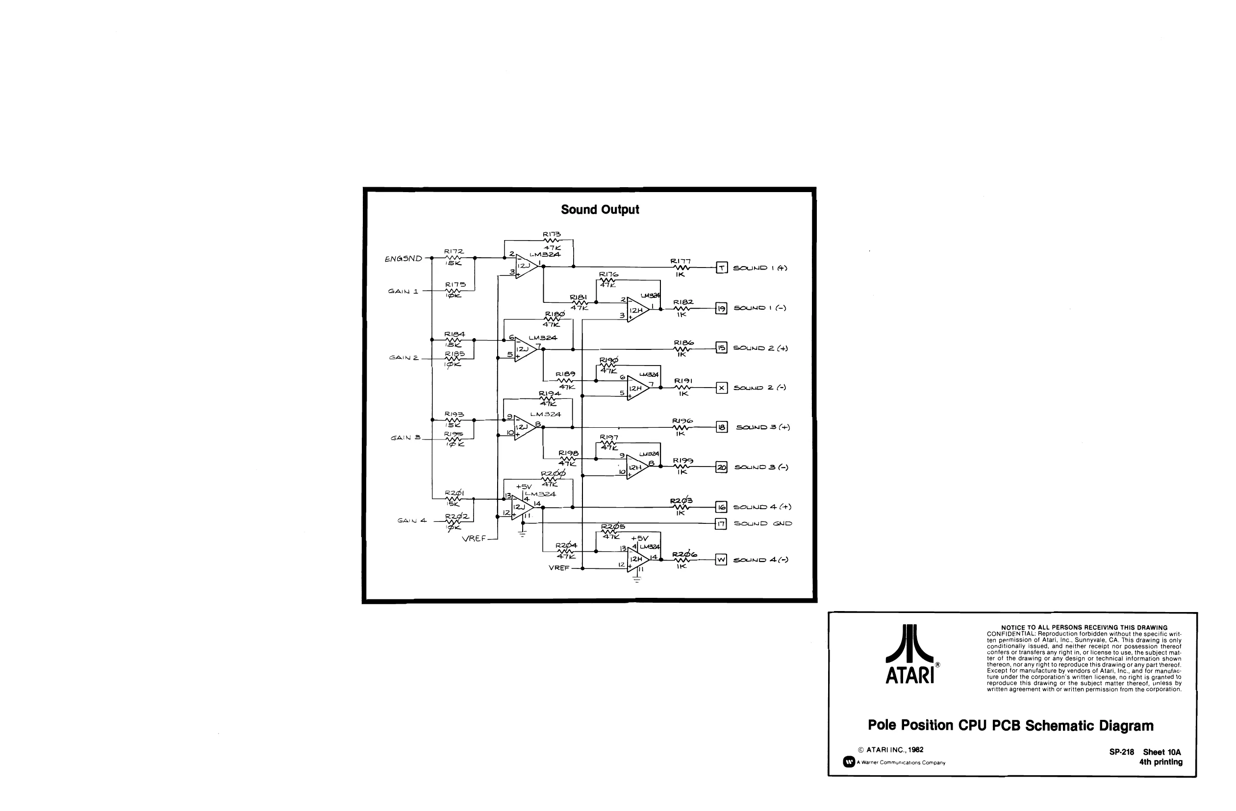
This page is a drawing, shown as the original scan.
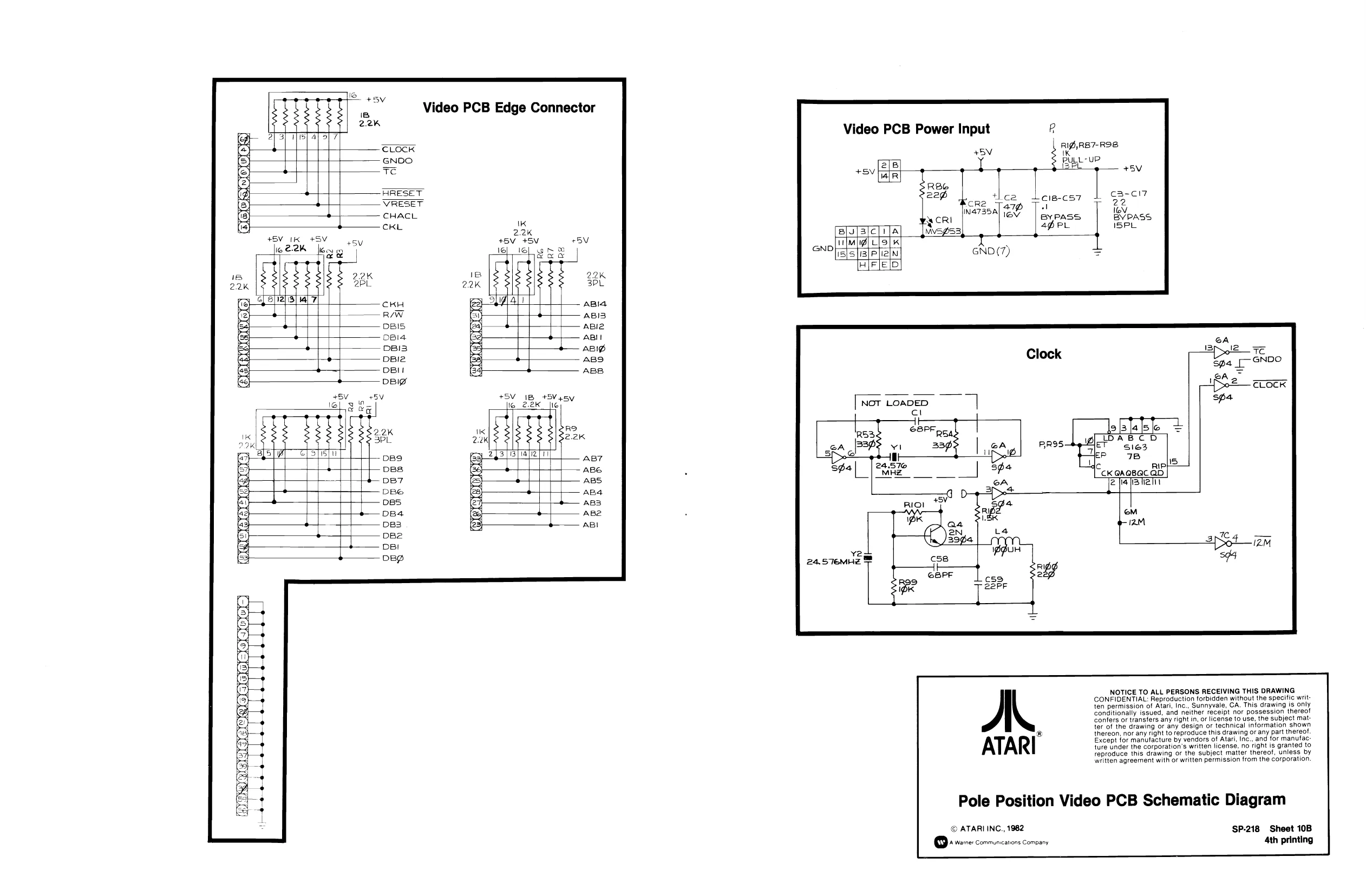
Video PCB Edge Connector
Video PCB Power Input
RB7-RSB +5V Ww 7 i PULL-UP tT BPC
RESET + VRESET
4} cnac {4} 4c. +5V cl8-C57 al r
BYPASS 4pPL | IK 22K IK
NOT LOADED cl iF a Rss, S8PF py debe id = meena 339) A 5 S163 at ee 7B 24.570 Ic RI 7 MHz ‘CK QA@BGCQD E la psheny
om iam
confers or transfers any right in, or license to use, the subject mat- NOTICE TO ALL PERSONS RECEIVING THIS DRAWING CONFIDENTIAL: Reproduction forbidden without the specific writ ten permission of Atari, Inc., Sunnyvale, CA. This drawing is only conditionally issued, and neither receipt nor possession thereof
ter of the drawing or any design or technical information shown I = ® thereon, nor any right to reproduce this drawing or any part thereof Except for manufacture by vendors of Atari, Inc., and for manutacture under the corporation's written license, no right is granted to reproduce this drawing or the subject matter thereof, unless by written agreement with or written permission from the corporation. il boeee
Pole Position Video PCB Schematic Diagram
© ATARI INC., 1982 SP-218 Sheet 10B
+ Warne: communcations Company 4th printing
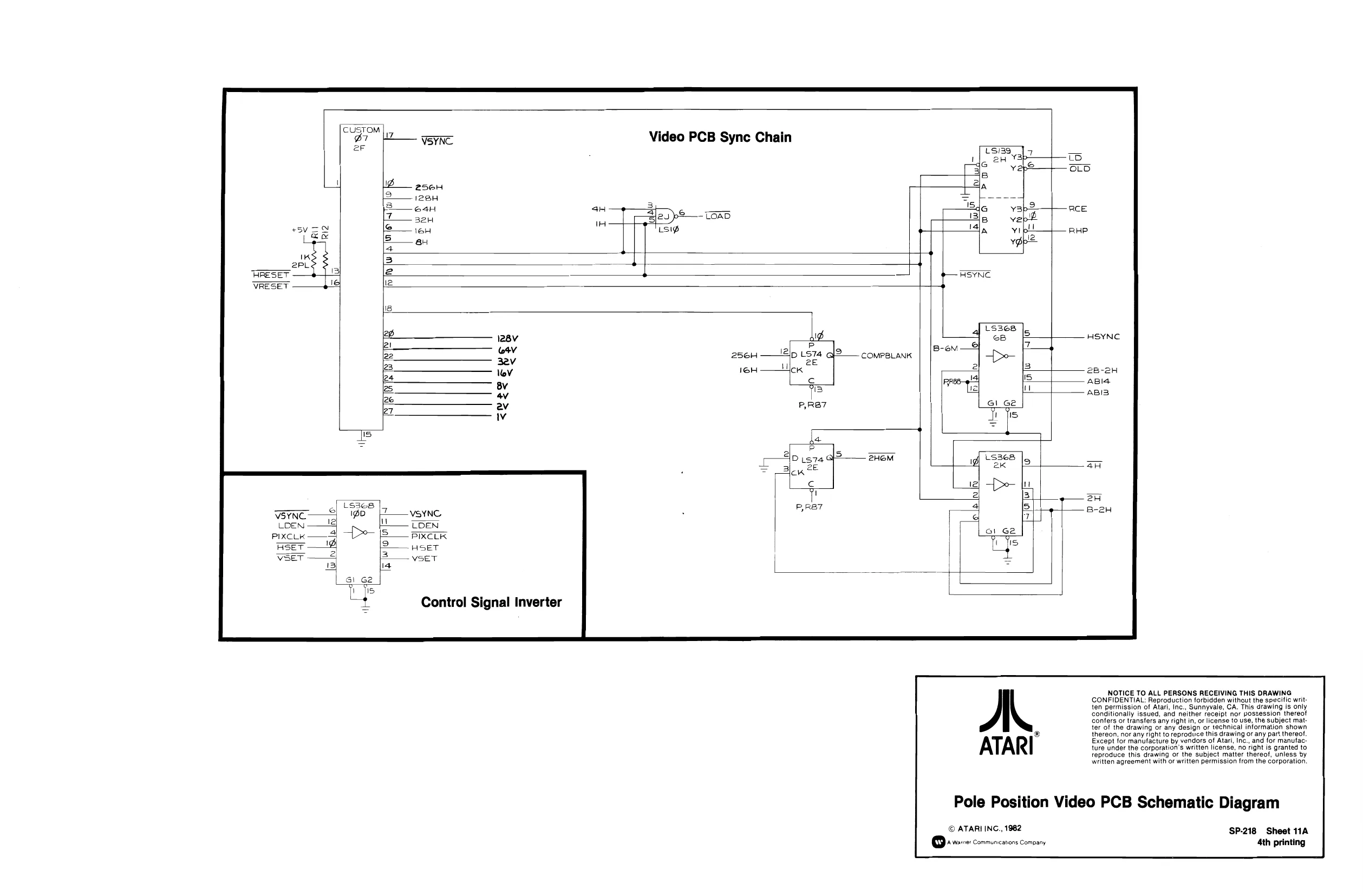
cugroM| Video PCB Sync Chain er
IK 2PL RESET t HSYNG VRESET
LS368 eB
COMPBLANK +p
VEYNC— 8) 80 VSYNC LDEN LOEN pixctk 4 —De- 8 PIXCLR HSET |o — HSET VSET -VSET 13 4 Gi G2 id ls
. Control Signal Inverter
NOTICE TO ALL PERSONS RECEIVING THIS DRAWING CONFIDENTIAL: Reproduction forbidden without the specific writ. ten permission of Atari, Inc., Sunnyvale, CA. This drawing is only conditionally issued, and neither receipt nor possession thereof confers or transfers any right in, or license to use, the subject matter of the drawing or any design or technical information shown ® thereon, nor any right to reproduce this drawing or any part thereof. Except for manufacture by vendors of Atari, Inc., and for manufac: ture under the corporation’s written license, no right is granted to reproduce this drawing or the subject matter thereof, unless by written agreement with or written permission {rom the corporation,
Pole Position Video PCB Schematic Diagram
© ATARI ING., 1982 SP-218 Sheet 11A + Were: Communications Company 4th printing
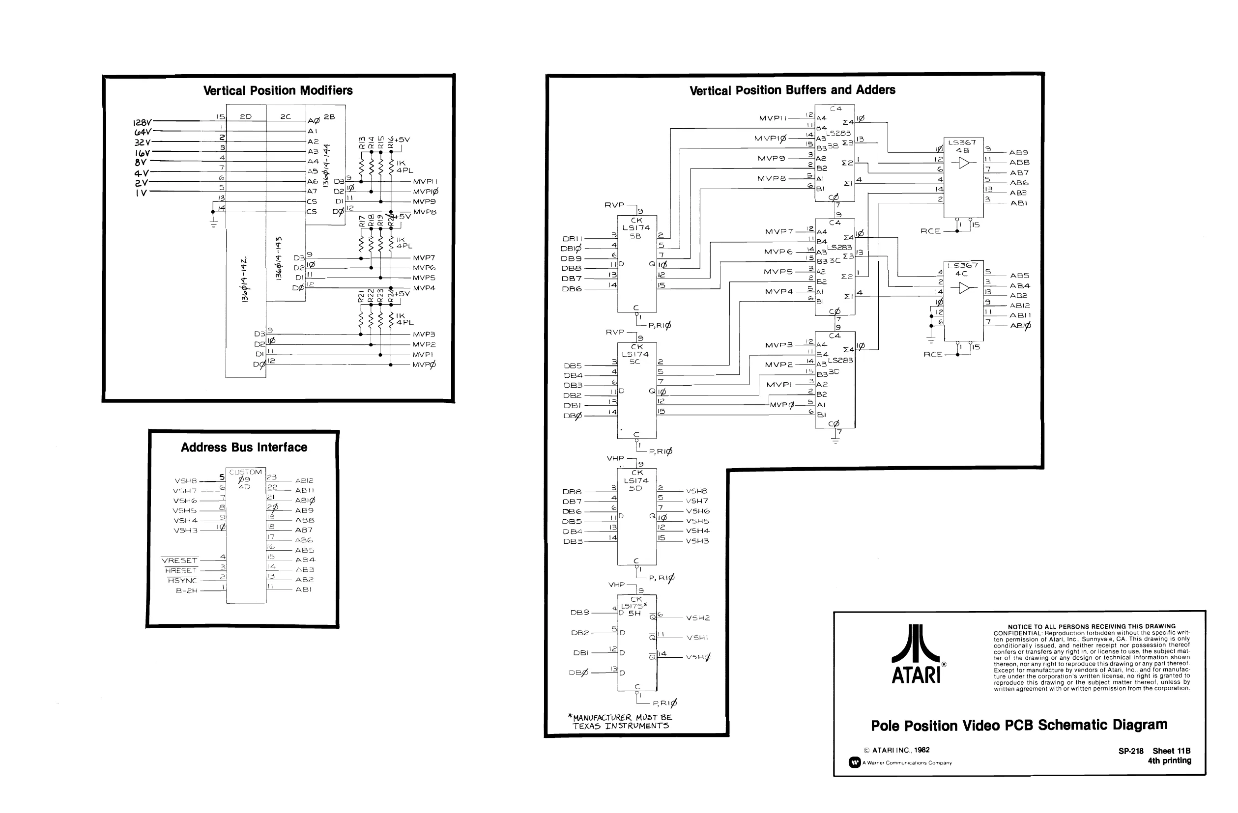
Vertical Position Buffers and Adders
Vertical Position Modifiers
2D ag 28
AY
a2
AS
a4 fas Lae 1A7 w 1314-144 LR 4S fu fo | > fw [rw | [ov
(BOP /4 143 136pl4-142
Address Bus Interface
CUSTOM p2 4D
VRESET
NOTICE TO ALL PERSONS RECEIVING THIS DRAWING CONFIDENTIAL: Reproduction forbidden without the specific written permission of Atari, Inc., Sunnyvale, CA. This drawing is only conditionally issued, and neither receipt nor possession thereof confers or transfers any right in, or license to use, the subject mat: ter of the drawing or any design or technical information shown thereon, nor any right to reproduce this drawing or any part thereof. ® Except for manufacture by vendors of Atari, Inc., and for manufac: ture under the corporation's written license, no right is granted to reproduce this drawing or the subject matter thereof, unless by written agreement with or written permission from the corporation.
XMANUFACTURER MUST BE. TEXAS INSTRUMENTS:
Pole Position Video PCB Schematic Diagram
© ATARI INC., 1982 SP-218 Sheet 11B
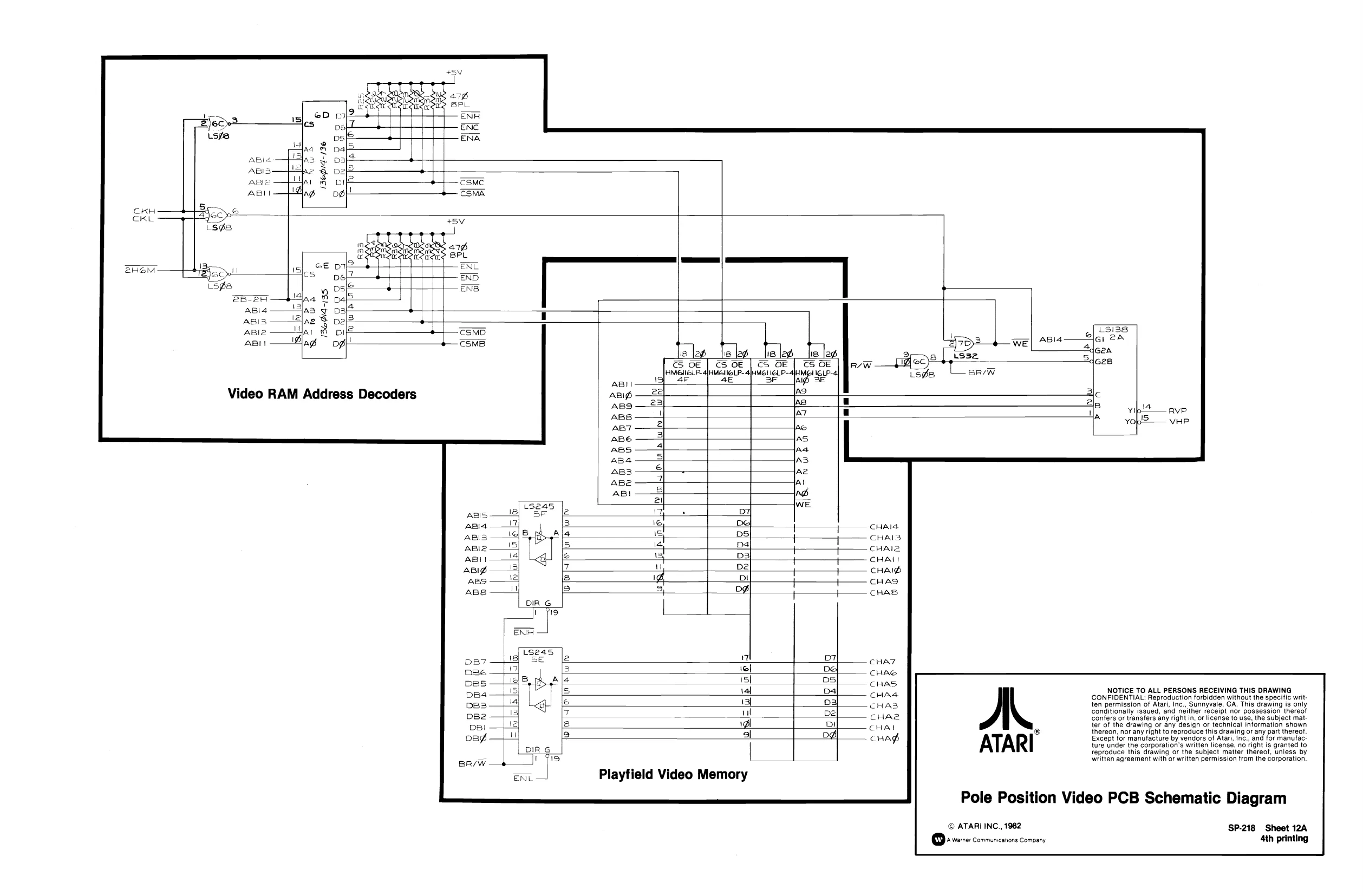
This page is a drawing, shown as the original scan.
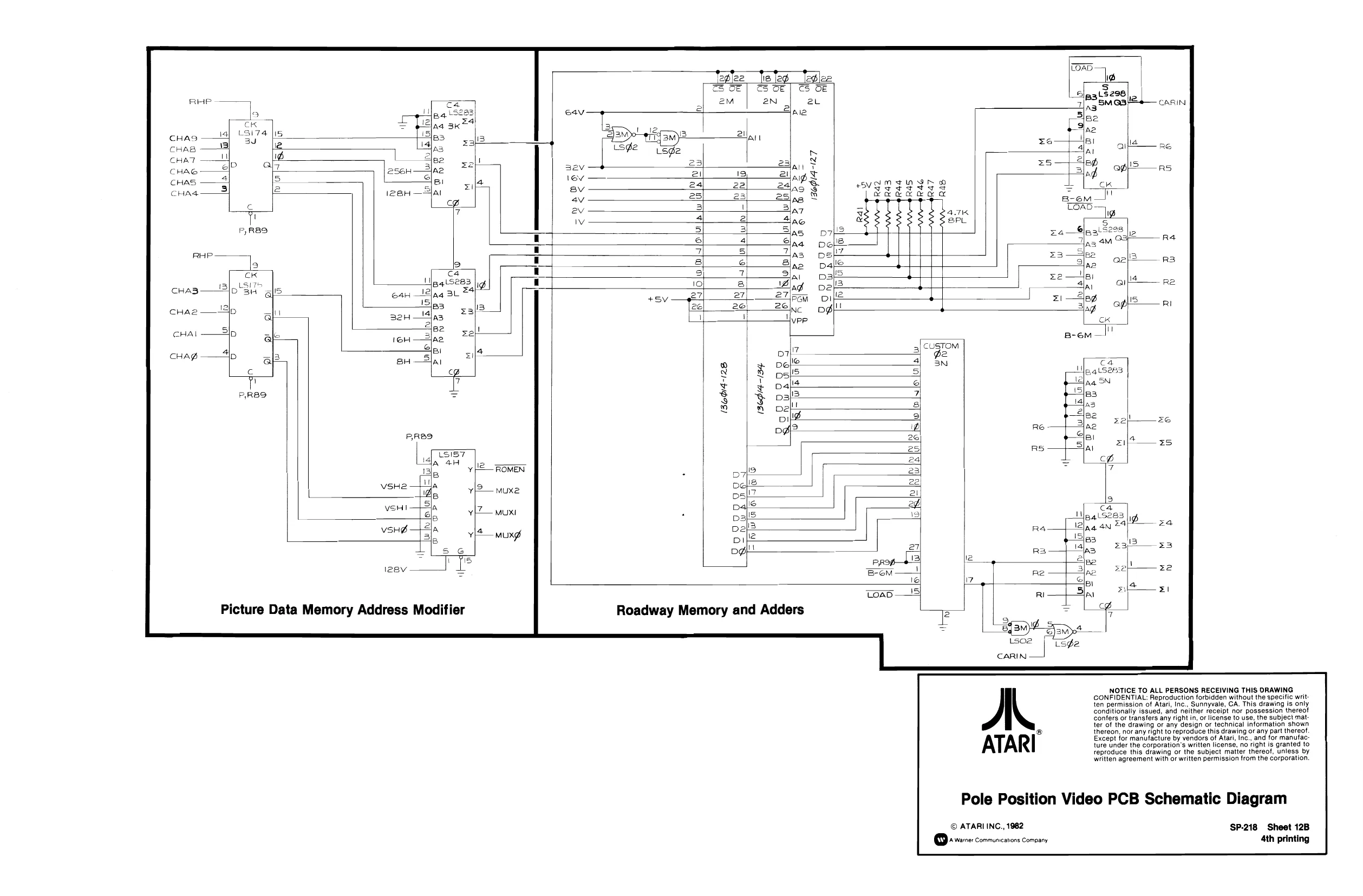
This page is a drawing, shown as the original scan.
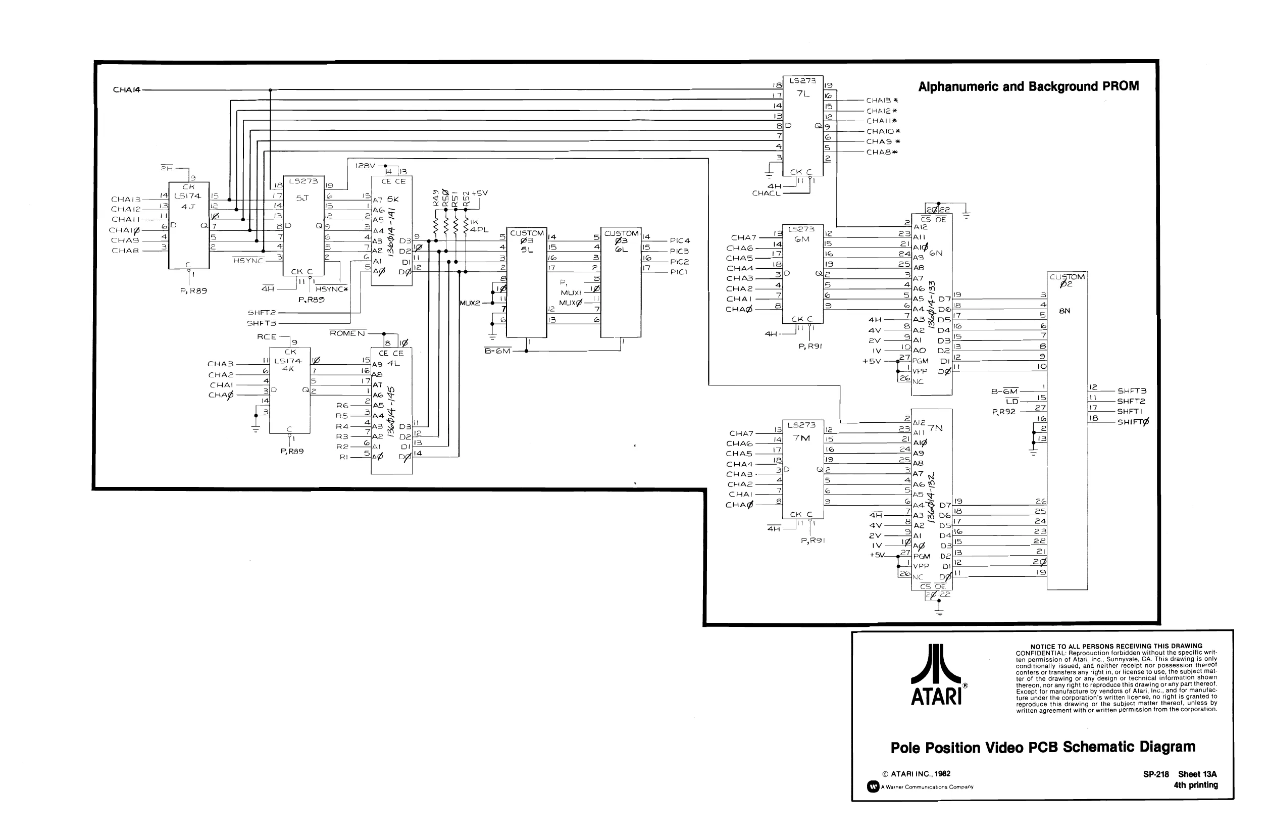
This page is a drawing, shown as the original scan.
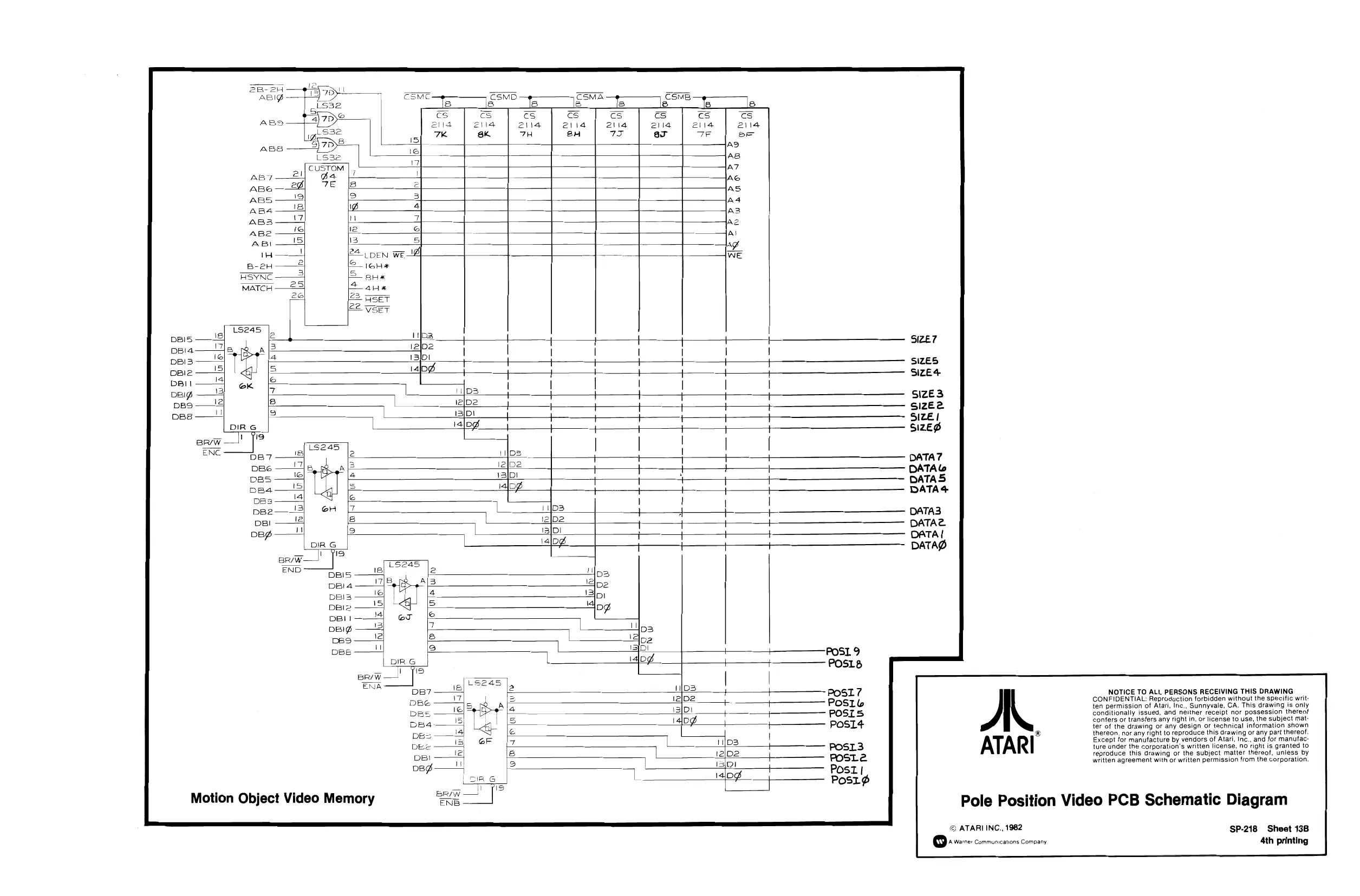
This page is a drawing, shown as the original scan.
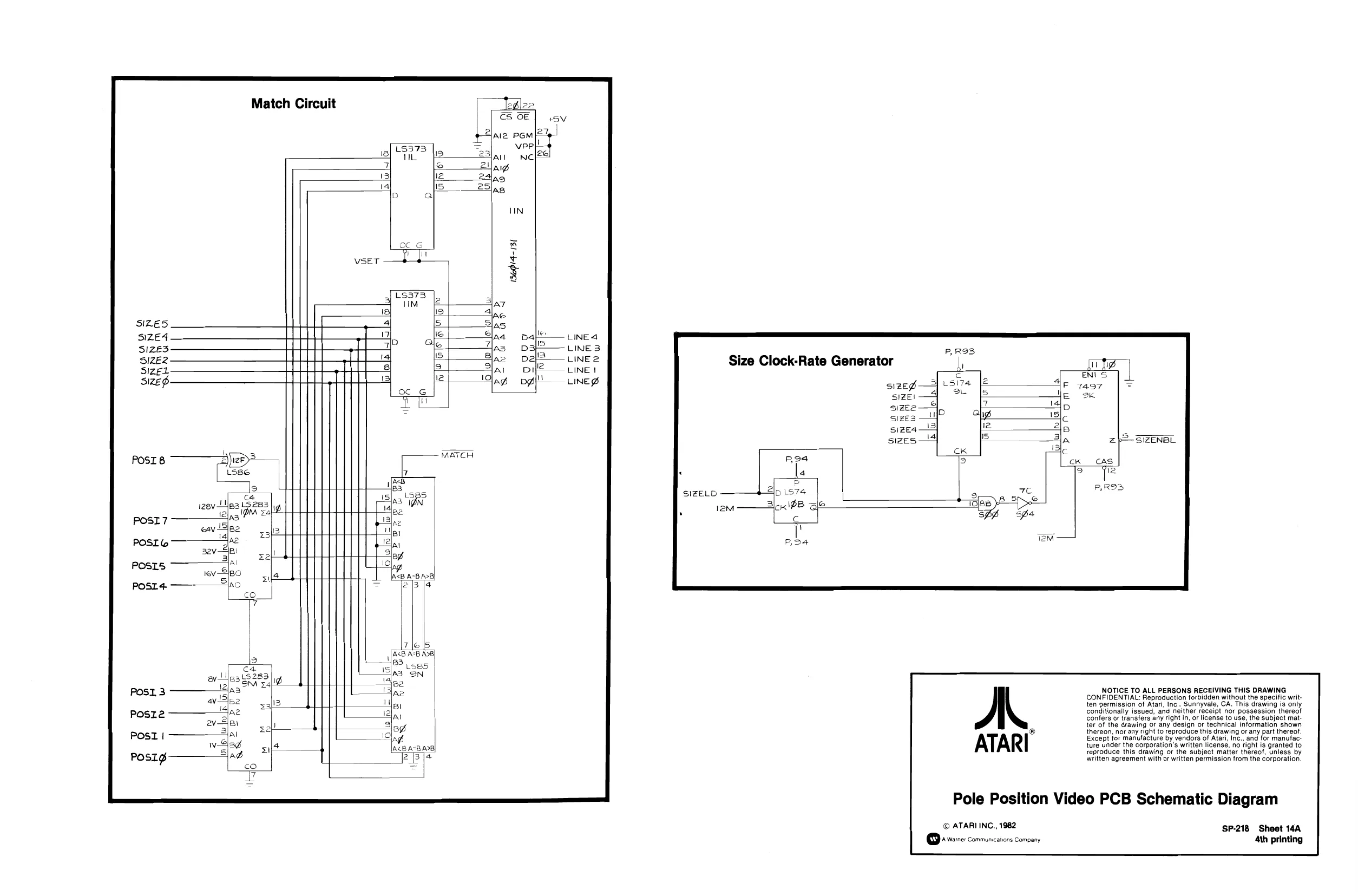
This page is a drawing, shown as the original scan.
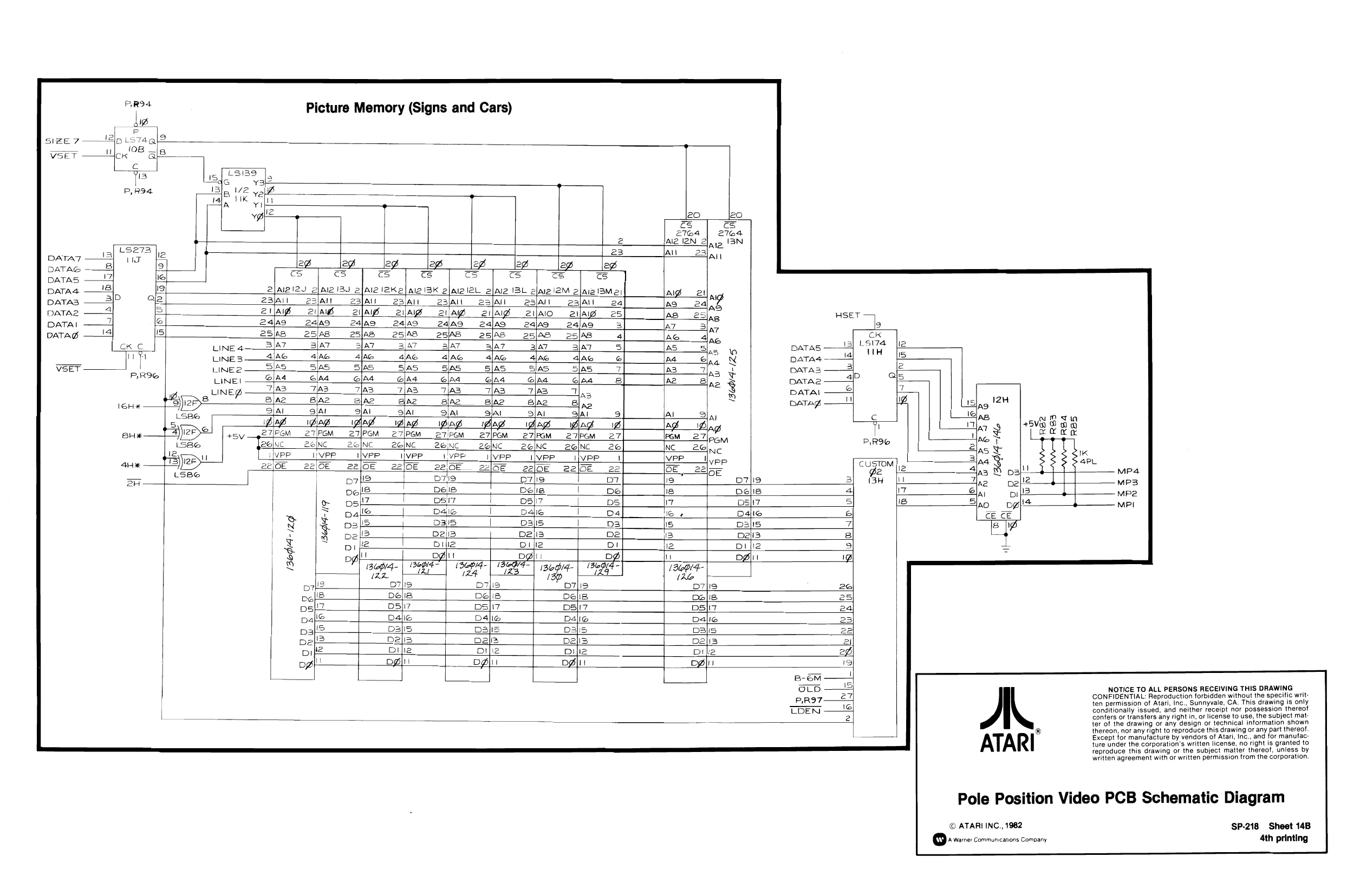
This page is a drawing, shown as the original scan.
This page is a drawing, shown as the original scan.
This page is a drawing, shown as the original scan.
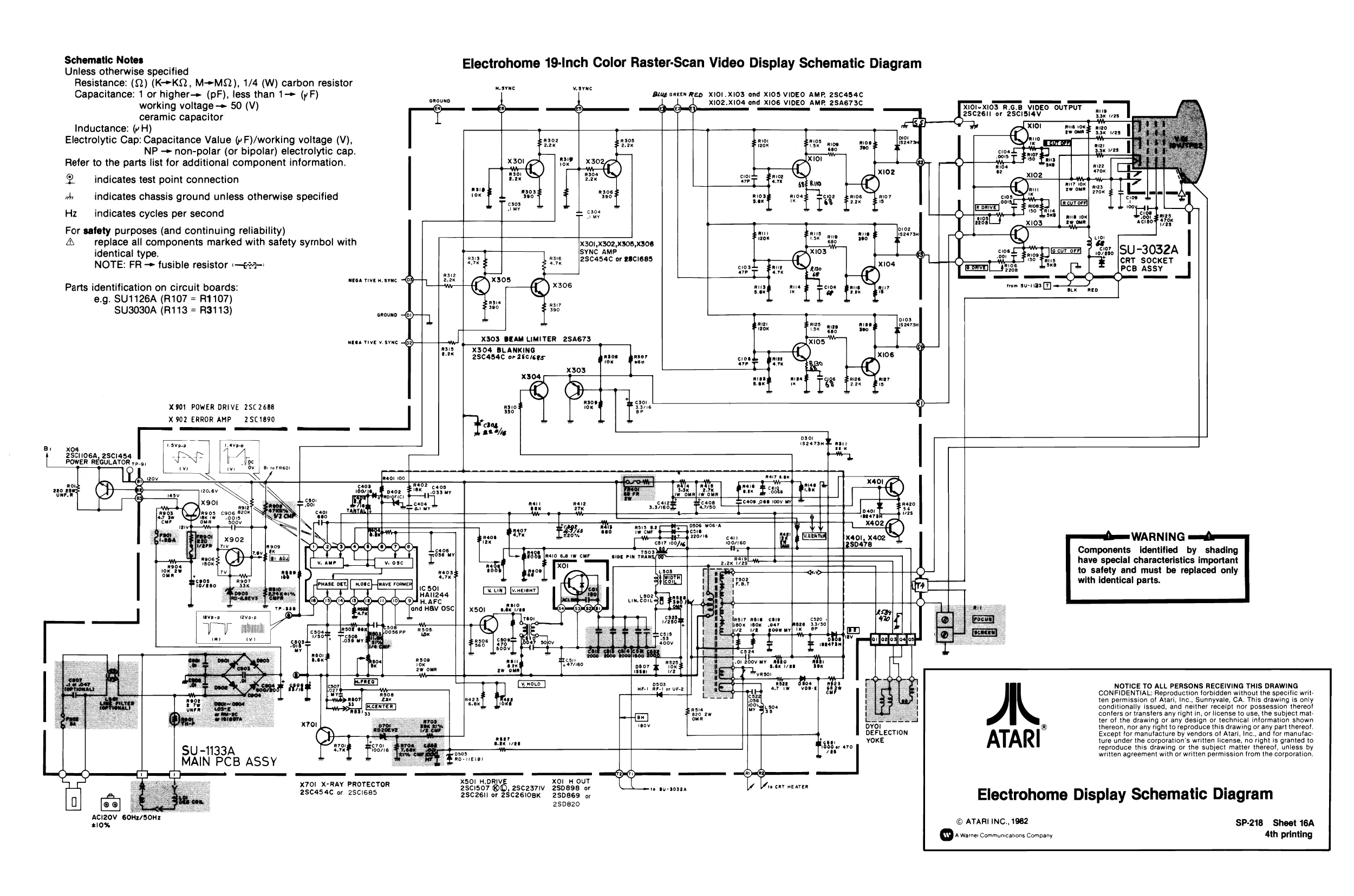
Schematic Notes Unless otherwise specified Resistance: (Q) (K->KQ, MM), 1/4 (W) carbon resistor Capacitance: 1 or higher-» (pF), less than 1 (yF) working voltage > 50 (V) ceramic capacitor Inductance: ( H) Electrolytic Cap: Capacitance Value (yF)/working voltage (V), NP — non-polar (or bipolar) electrolytic cap. Refer to the parts list for additional component information.
Q indicates test point connection
hy indicates chassis ground unless otherwise specified
Hz indicates cycles per second
For safety purposes (and continuing reliability) 4 replace all components marked with safety syrnbol with identical type.
NEGA TIVE ¥.SYNC
X901 POWER DRIVE 2S¢ 2688
X902 ERROR AMP 2SC1890
ray Roun wesene vesync
Electrohome 19-Inch Color Raster-Scan Video Display Schematic Diagram
Blug oxen RED X101.X103 and X15 VIDEO AMP, 2SC454C X102.X104 and XI06 VIDEO AMP. 2SA673C
ane tox
SYNC AMP
wis, Pier
Br x09 2SCIIOGA, 2501454 POWER REGULATOR rp.5, ° B:roFR6Or
fnsor 00 X303 BEAM LIMITER 2SA673 'x301,x302,X305,x308 AM 2SC454C or RBCI6ES
X304 BLANKING 2SC4B4C oF 26c/ces noe
Rok Bo
Cr Po X101-x103-R.G.B VIDEO OUTPUT 2SC26II of 2SCISI4V
R26 2k 7 tow or | a2 aw ome | Brom
ISU-3032A | CRT SOCKET gee |
nae Bid
waMr
fpuase oe] hp
Bia Kc
x7o1
SU-1133A
MAIN PCB ASSY
ea] ACIZ0V 60H2/50Hz 210% e701 eerie be or ttov wy -Affe ote Tan
- meer Citi 508 a 5 RO-IEC@)
X7OI_ X-RAY PROTECTOR 2SC454C or 25c1685 X501_H.ORIV XOl HO 28C1507 ©Q, 2sc237Iv 280898 or 2SC26Il or ZSC2610BK 280869 or UT
280820 ta ORT MEATER
Electrohome Display Schematic Diagram
© ATARI INC., 1962
NOTICE TO ALL PERSONS RECEIVING THIS DRAWING CONFIDENTIAL: Reproduction forbidden without the specific writ ten permission of Atari, Inc., Sunnyvale, CA. This drawing is only conditionally issued, and neither receipt nor possession thereof confers or transfers any right in, or license to use, the subject matter of the drawing or any design or technical information shown
thereon, nor any right to reproduce this drawing or any part thereof,
Except for manutacture by vendors of Atari, Inc., and for manufacture under the corporation's written license, no right is granted to reproduce this drawing or the subject matter thereof, unless by written agreement with or written permission from the corporation.
SP-218 Sheet 16A
This page is a drawing, shown as the original scan.