Fast Freddie SP-208 1st Printing
Fly-Boy (Kaneko, 1982) · Schematic Package · 26 pages · 26 sections · original scan
This page is a drawing, shown as the original scan.
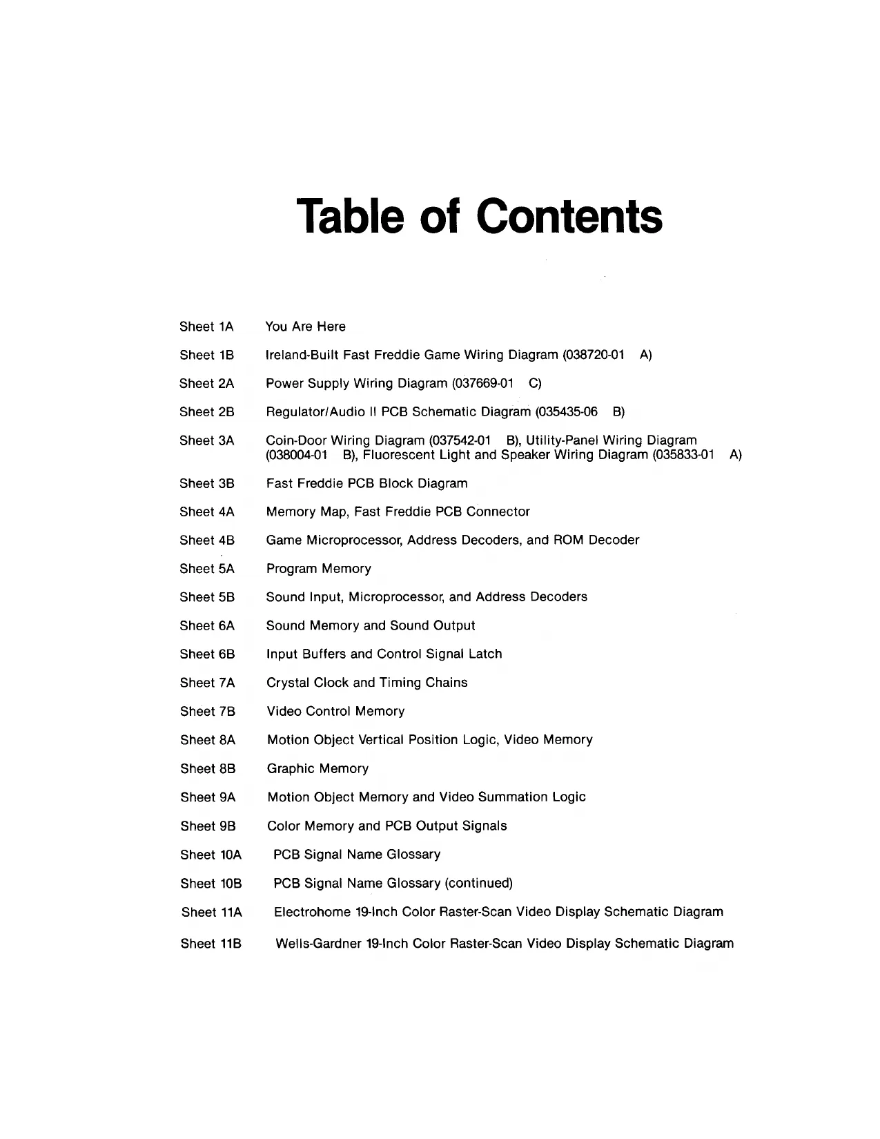
Sheet 1A
Sheet 1B
Sheet 2A
Sheet 2B
Sheet 3A
Sheet 3B
Sheet 4A
Sheet 4B
Sheet 5A
Sheet 5B
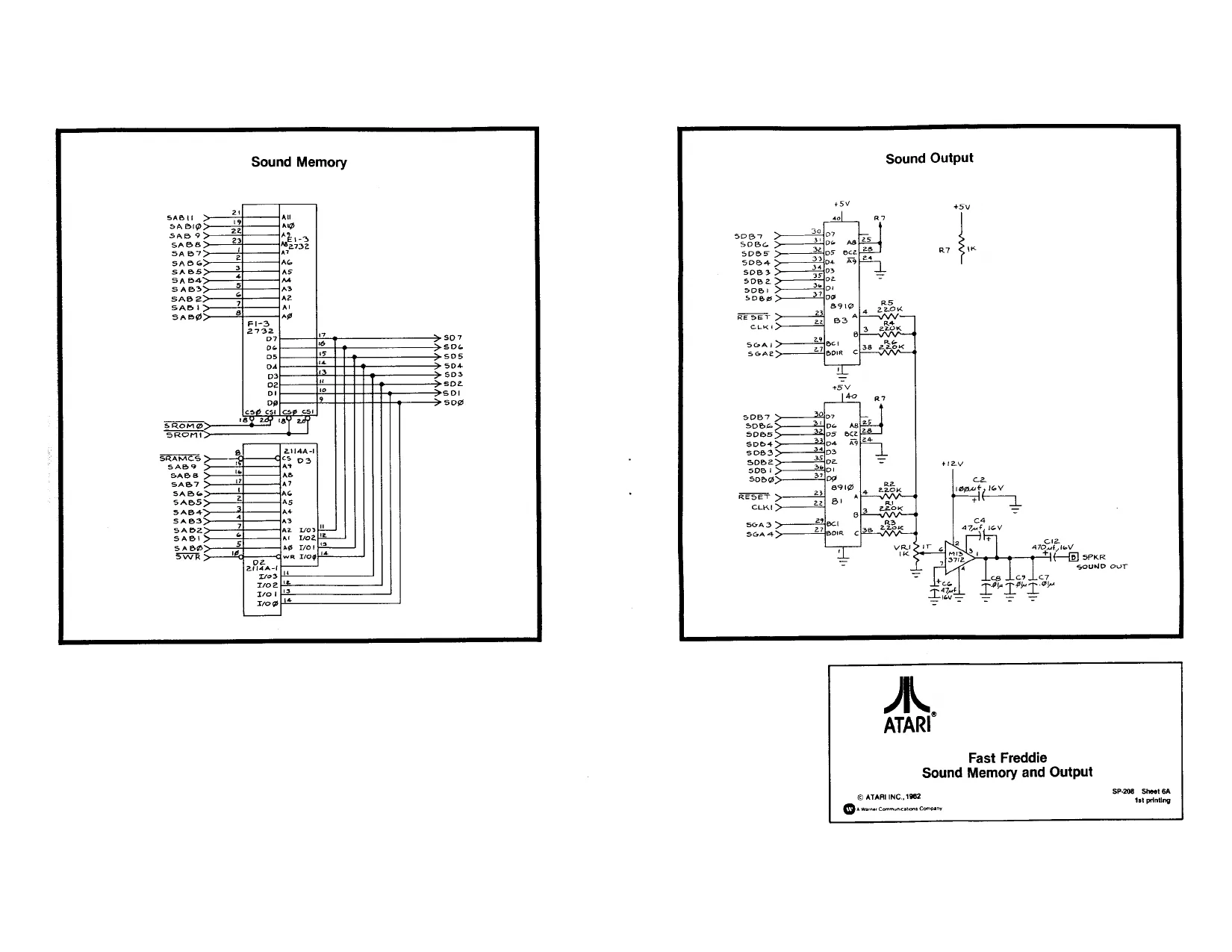
Sheet 6A
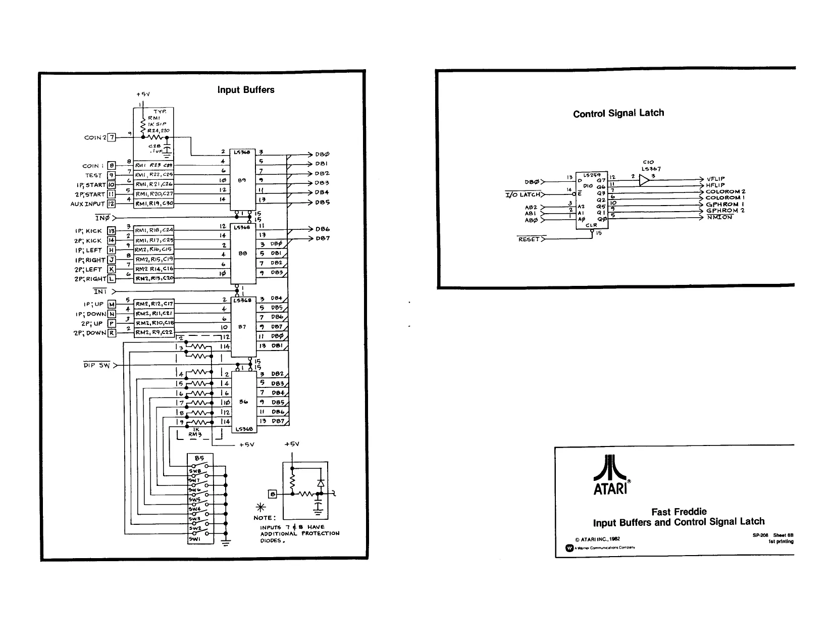
Sheet 6B
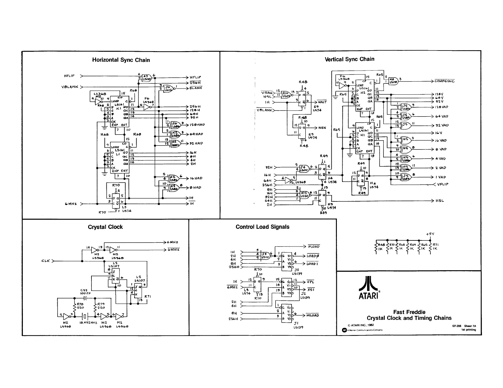
Sheet 7A
Sheet 7B
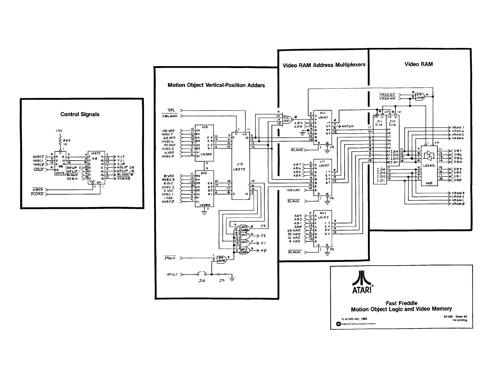
Sheet 8A
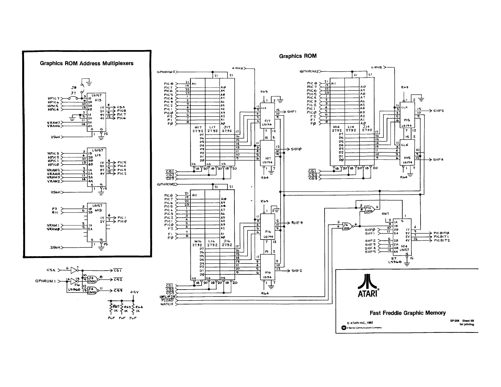
Sheet 8B
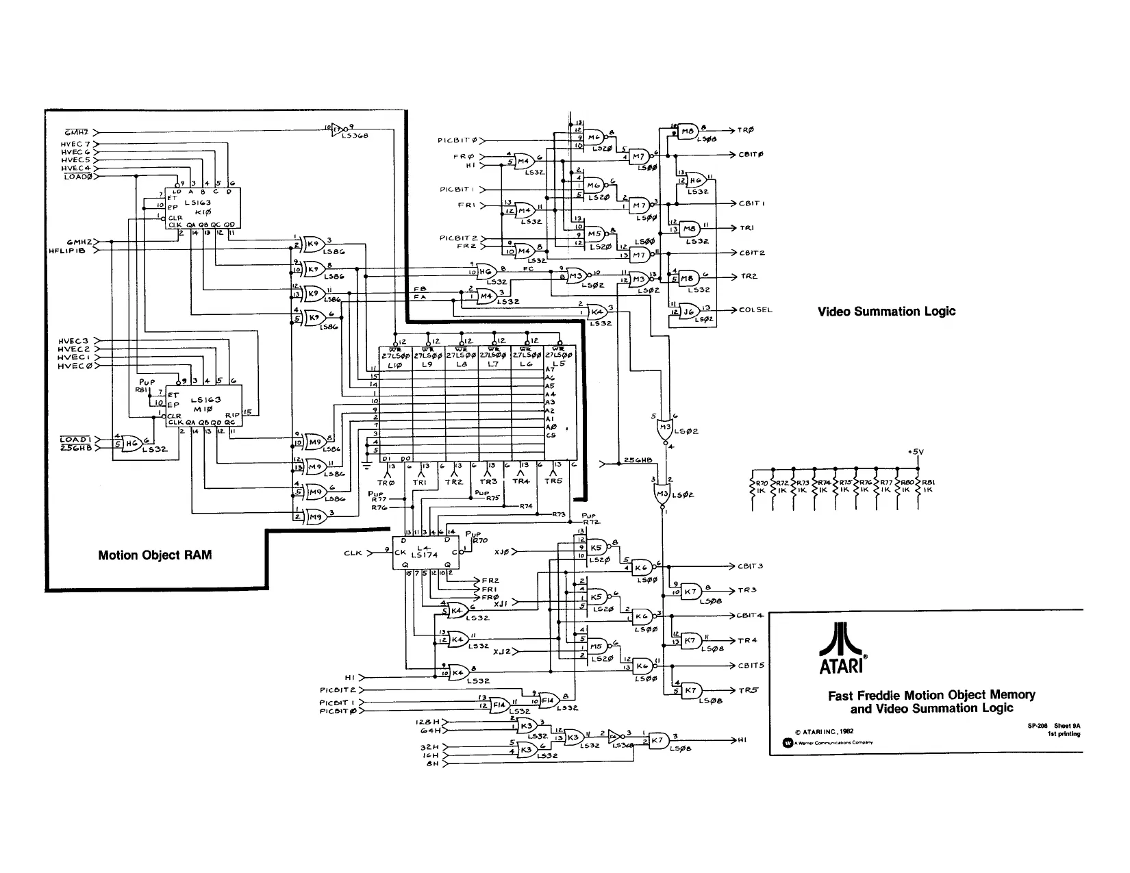
Sheet 9A
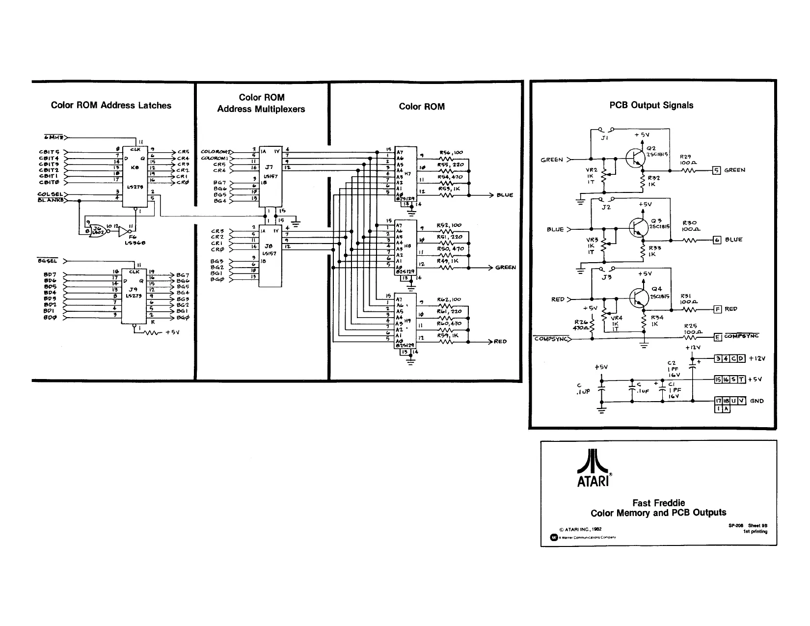
Sheet 9B
Sheet 10A
Sheet 10B
Sheet 11A
Sheet 11B Table of Contents
You Are Here
lreland-Built Fast Freddie Game Wiring Diagram (038720-01 A)
Power Supply Wiring Diagram (037669-01 CC)
Regulator/Audio || PCB Schematic Diagram (035435-06 _B)
Coin-Door Wiring Diagram (037542-01 _B), Utility-Panel Wiring Diagram (038004-01 B), Fluorescent Light and Speaker Wiring Diagram (035833-01 A)
Fast Freddie PCB Block Diagram
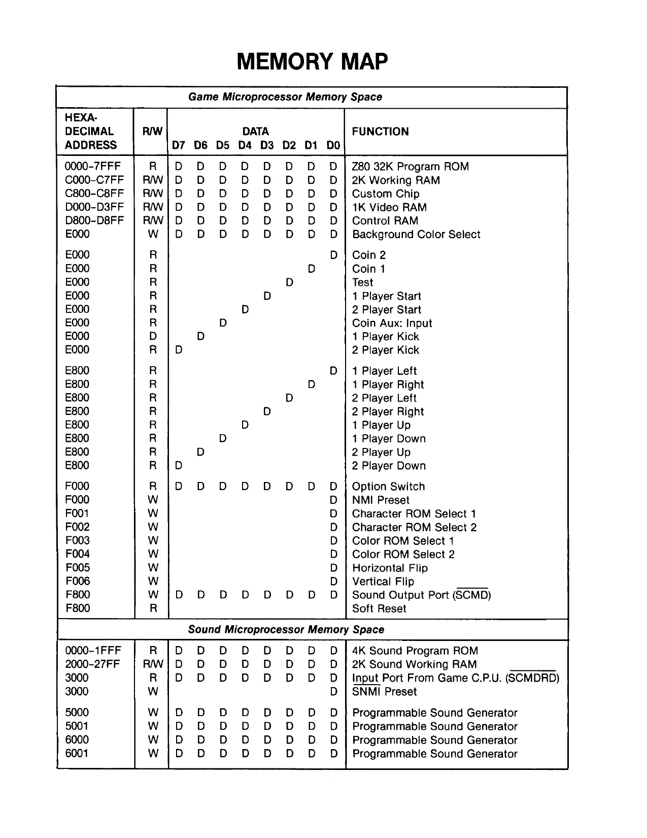
Memory Map, Fast Freddie PCB Connector
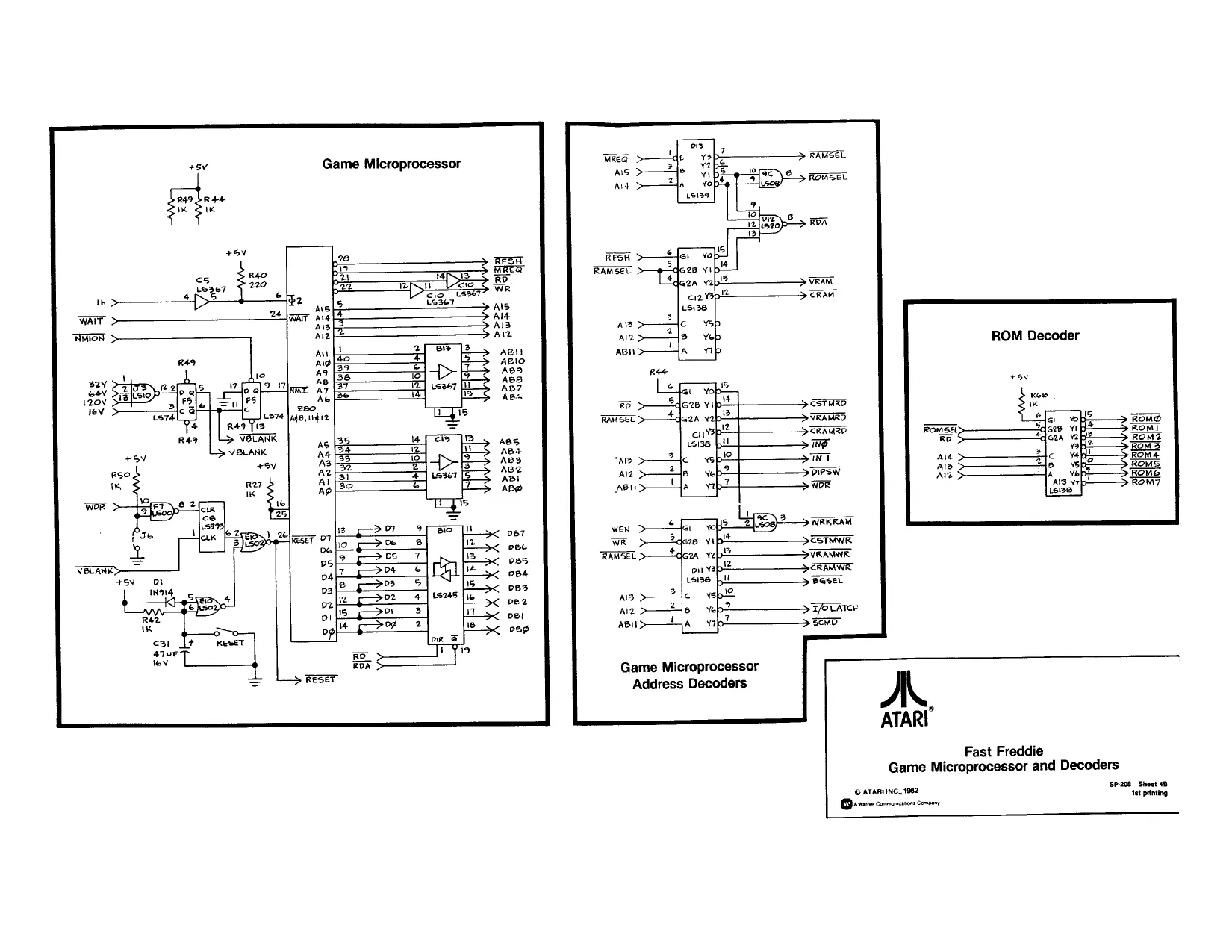
Game Microprocessor, Address Decoders, and ROM Decoder
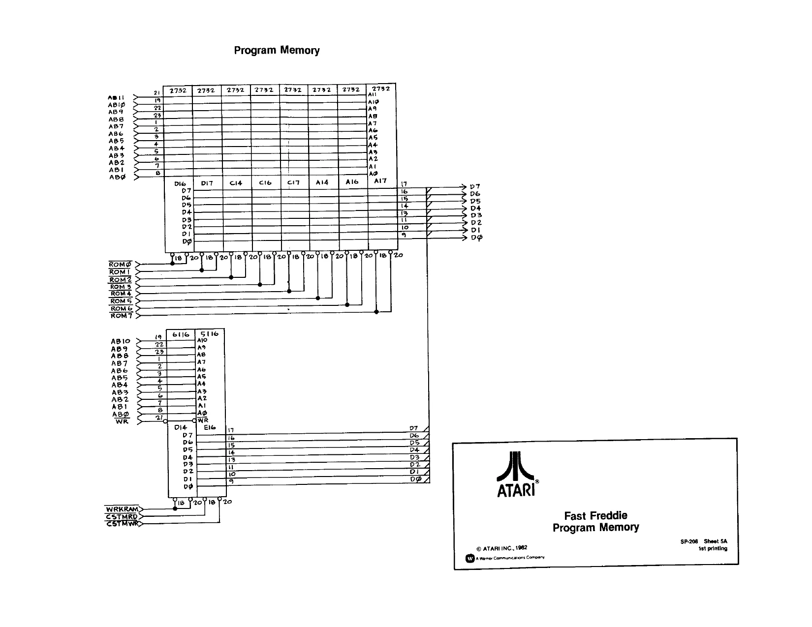
Program Memory
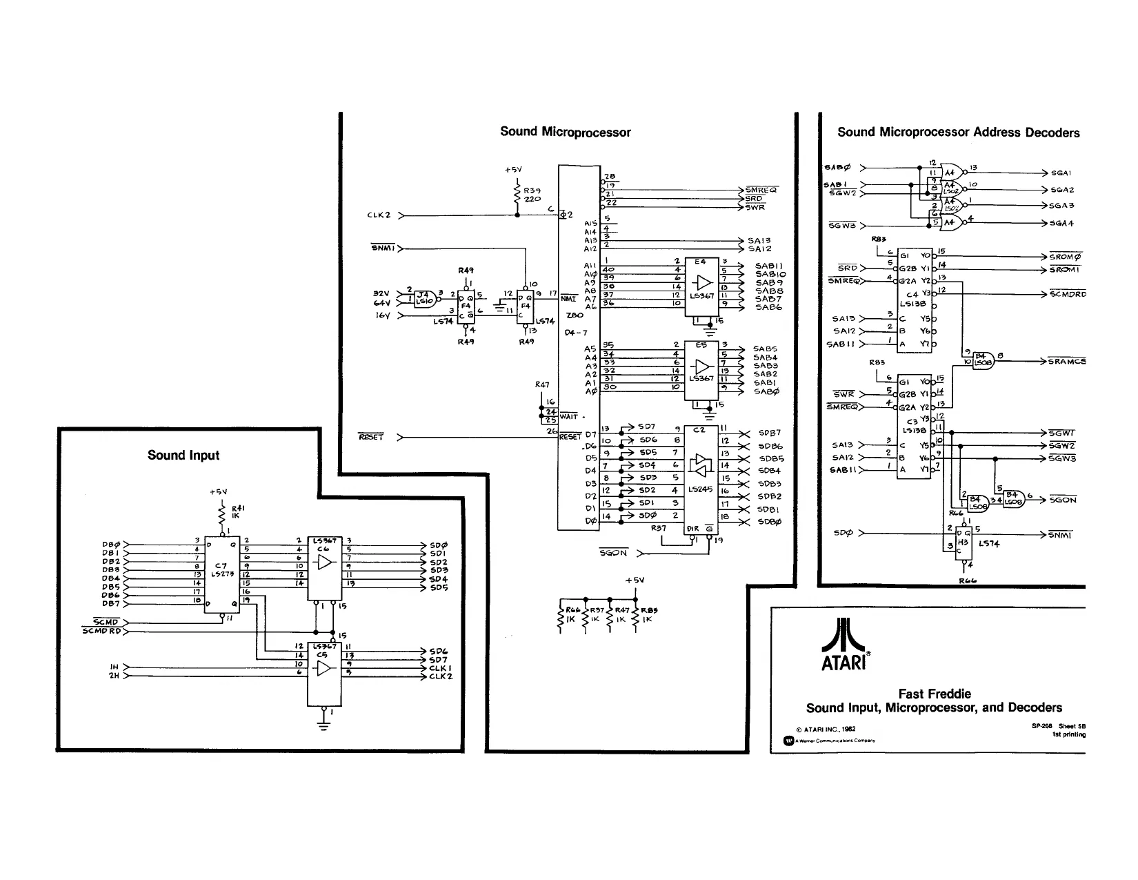
Sound Input, Microprocessor, and Address Decoders
Sound Memory and Sound Output
Input Buffers and Control Signal Latch
Crystal Clock and Timing Chains
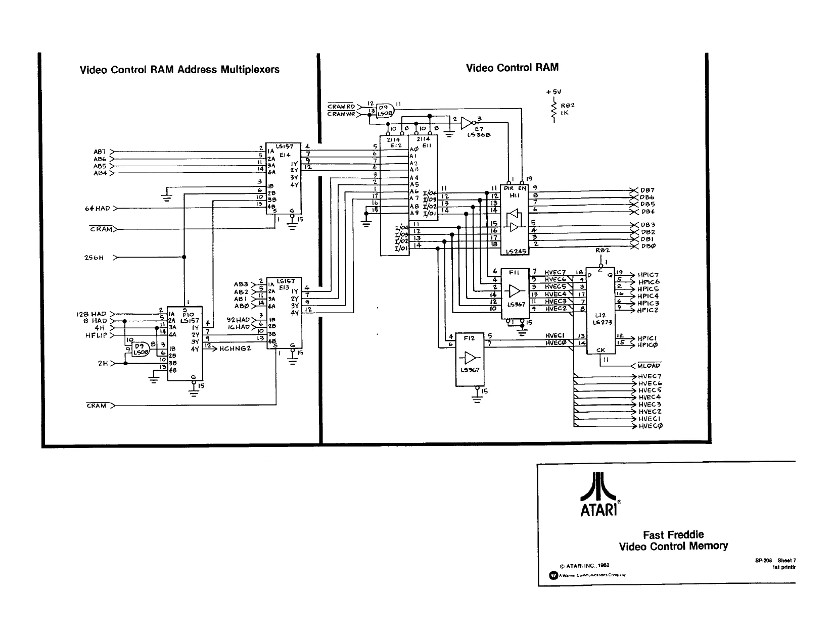
Video Control Memory
Motion Object Vertical Position Logic, Video Memory
Graphic Memory
Motion Object Memory and Video Summation Logic
Color Memory and PCB Output Signals
PCB Signal Name Glossary
PCB Signal Name Glossary (continued)
Electrohome 19-Inch Color Raster-Scan Video Display Schematic Diagram
Wells-Gardner 19-Inch Color Raster-Scan Video Display Schematic Diagram
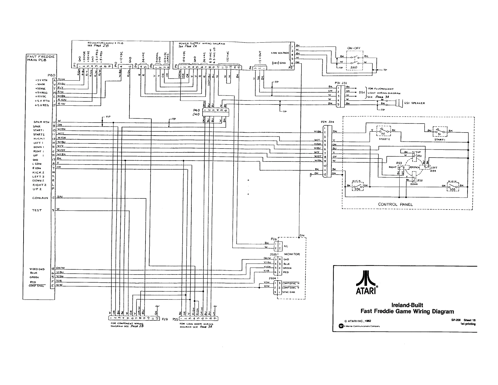
This page is a drawing, shown as the original scan.
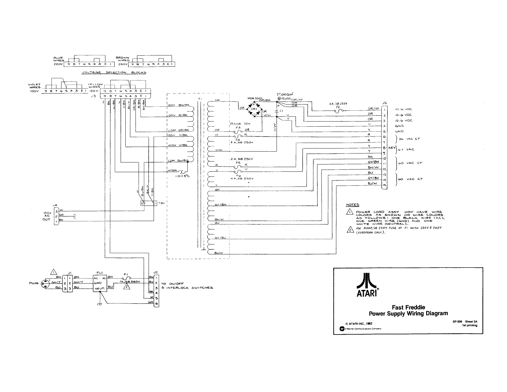
This page is a drawing, shown as the original scan.
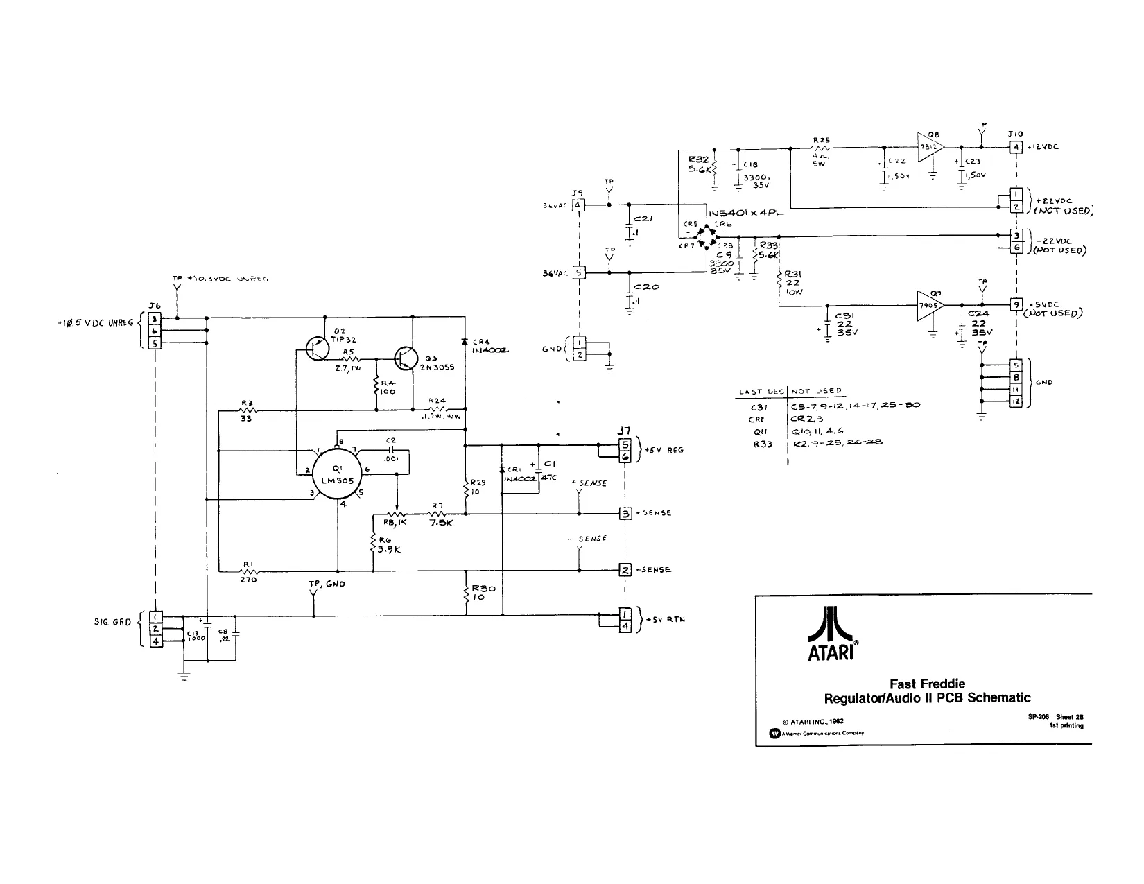
This page is a drawing, shown as the original scan.
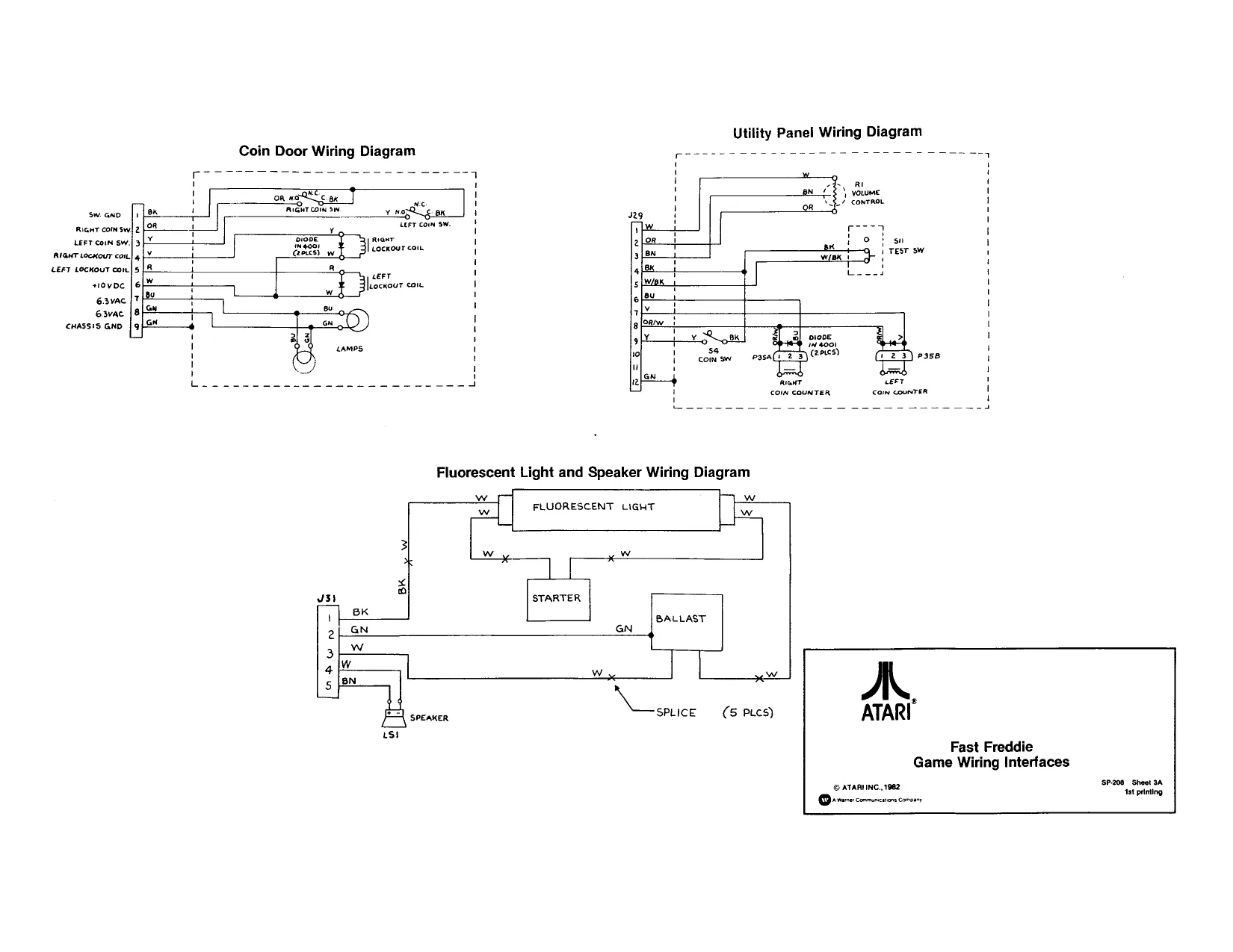
This page is a drawing, shown as the original scan.
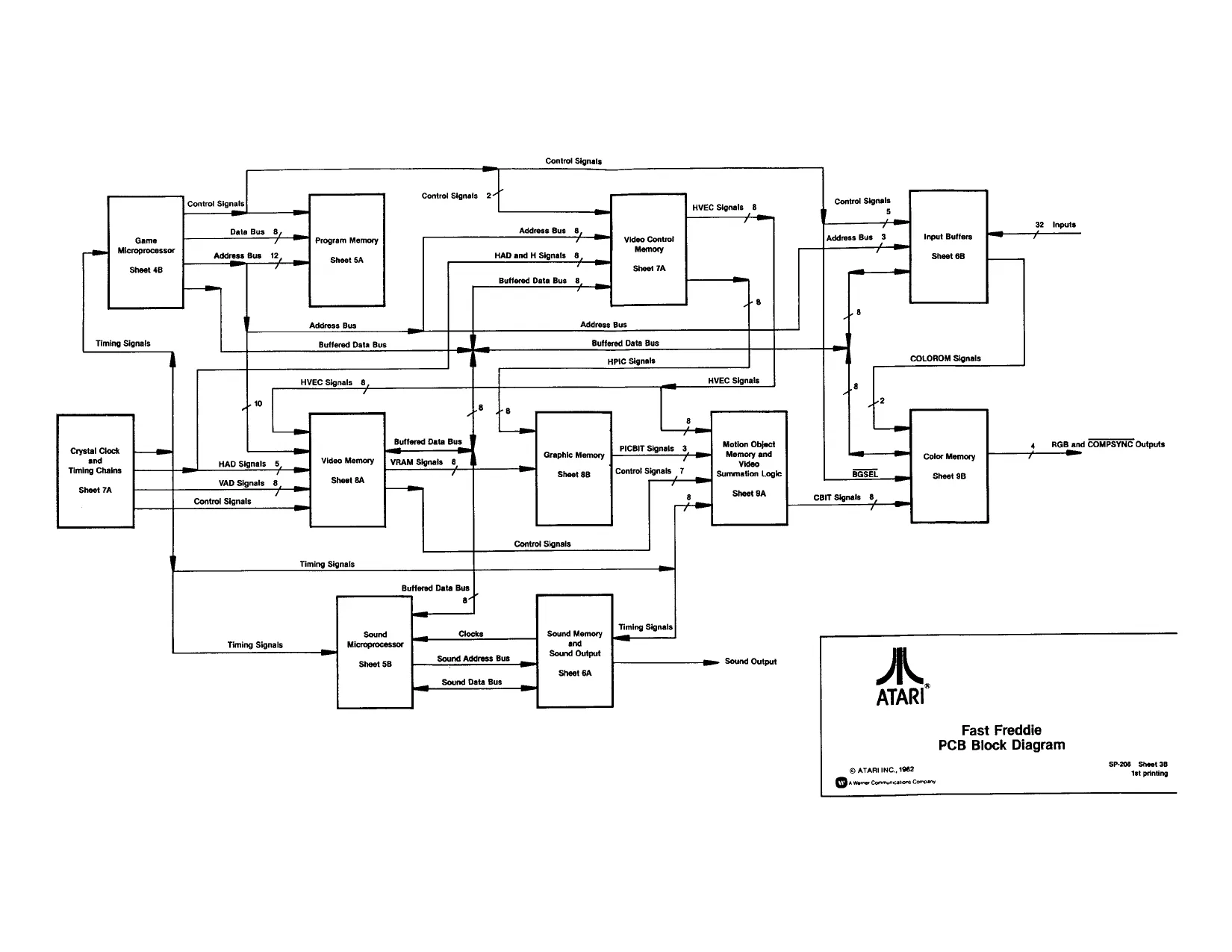
This page is a drawing, shown as the original scan.
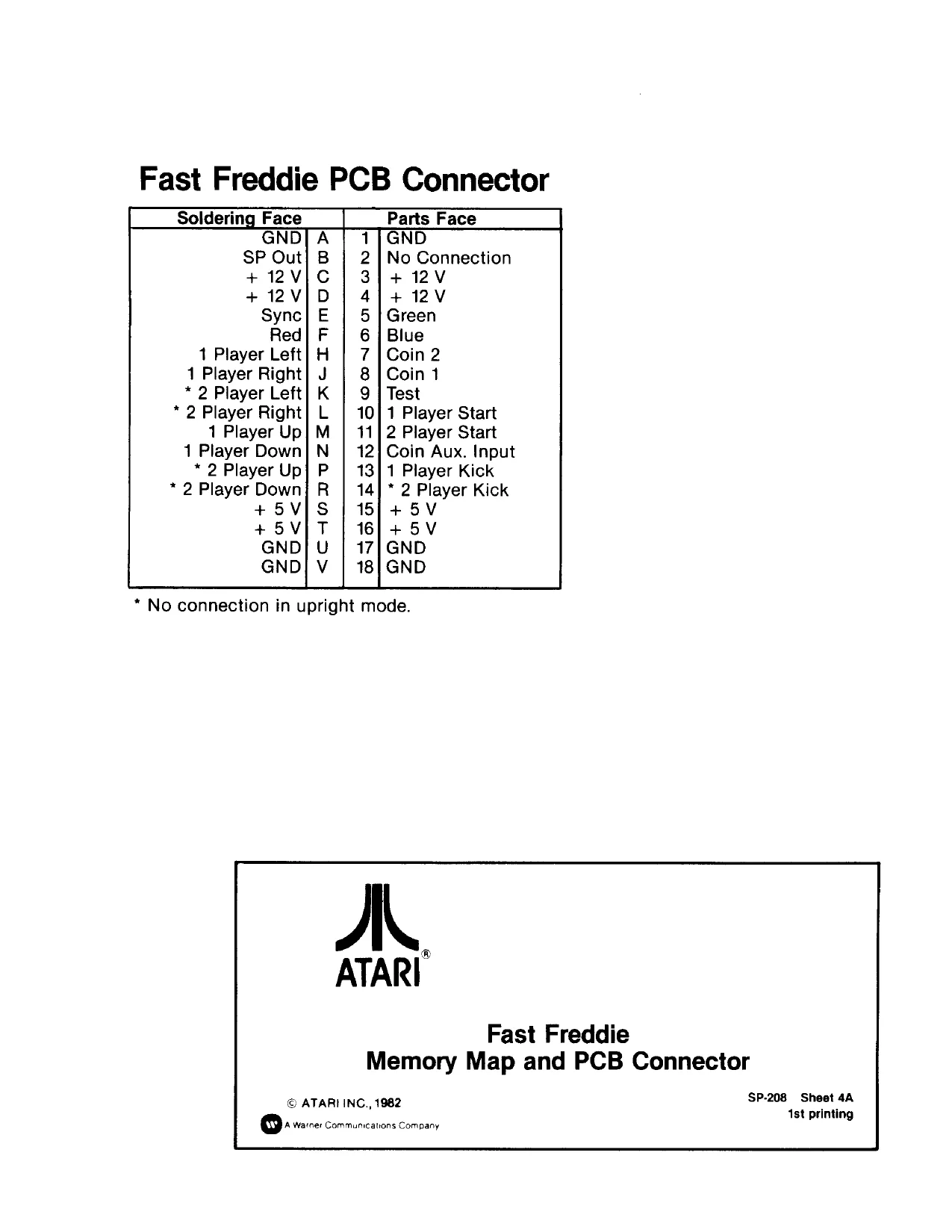
This page is a drawing, shown as the original scan.
This page is a drawing, shown as the original scan.
This page is a drawing, shown as the original scan.
This page is a drawing, shown as the original scan.
This page is a drawing, shown as the original scan.
This page is a drawing, shown as the original scan.
This page is a drawing, shown as the original scan.
This page is a drawing, shown as the original scan.
This page is a drawing, shown as the original scan.
This page is a drawing, shown as the original scan.
This page is a drawing, shown as the original scan.
This page is a drawing, shown as the original scan.
This page is a drawing, shown as the original scan.
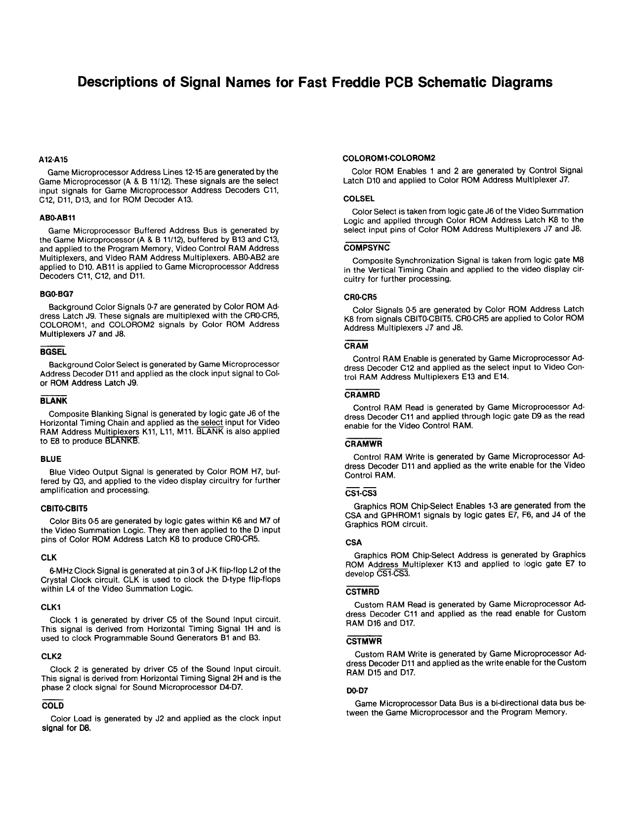
Descriptions of Signal Names for Fast Freddie PCB Schematic Diagrams
AIZ-A1S Game Microprocessor Address Lines 12-15 are generated by the Game Microprocessor (A & B 11/12). These signals are the select input signals for Game Microprocessor Address Decoders C11, C12, D11, D13, and for ROM Decoder A13.
ABO-AB11 Game Microprocessor Buffered Address Bus is generated by the Game Microprocessor (A & B 11/12), buffered by B13 and C13, and applied to the Program Memory, Video Control RAM Address Multiplexers, and Video RAM Address Multiplexers. ABO-AB2 are applied to D10. AB11 is applied to Game Microprocessor Address Decoders C11, C12, and D11.
BGO-BG7 Background Color Signals 0-7 are generated by Color ROM Address Latch J9. These signals are multiplexed with the CRO-CRS, COLOROM1, and COLORON2 signals by Color ROM Address Multiplexers J7 and J8.
BGSEL Background Color Select is generated by Game Microprocessor Address Decoder D11 and applied as the clock input signal to Color ROM Address Latch J9.
BLANK Composite Blanking Signal is generated by logic gate J6 of the Horizontal Timing Chain and applied as the select input for Video RAM Address Multiplexers K11, L11, M11. BLANK is also applied to E8 to produce SLANKE.
BLUE Blue Video Output Signal is generated by Color ROM H7, butfered by Q3, and applied to the video display circuitry for further amplification and processing.
CBITO-CBITS Color Bits 0-5 are generated by logic gates within K6 and M7 of the Video Summation Logic. They are then applied to the D input pins of Color ROM Address Latch K8 to produce CRO-CRS5.
CLK 6-MHz Clock Signal is generated at pin 3 of J-K flip-flop L2 of the Crystal Clock circuit. CLK is used to clock the D-type flip-flops within L4 of the Video Summation Logic.
CLK Clock 1 is generated by driver C5 of the Sound Input circuit. This signal is derived from Horizontal Timing Signal 1H and is used to clock Programmable Sound Generators B1 and B3.
CLK2 Clock 2 is generated by driver C5 of the Sound Input circuit. This signal is derived from Horizontal Timing Signal 2H and is the phase 2 clock signal for Sound Microprocessor D4-D7.
COLD Color Load is generated by J2 and applied as the clock input ‘signal for D8. COLOROM1-COLOROM2 Color ROM Enables 1 and 2 are generated by Control Signal Latch D10 and applied to Color ROM Address Multiplexer J7.
COLSEL Color Select is taken from logic gate J6 of the Video Summation Logic and applied through Color ROM Address Latch K8 to the select input pins of Color ROM Address Multiplexers J7 and J8.
COMPSYNC. Composite Synchronization Signal is taken from logic gate MB in the Vertical Timing Chain and applied to the video display circuitry for further processing.
CRO-CRS Color Signals 0-5 are generated by Color ROM Address Latch K8 from signals CBITO-CBITS. CRO-CRS are applied to Color ROM Address Multiplexers J7 and J8.
CRAM Control RAM Enable is generated by Game Microprocessor Address Decoder C12 and applied as the select input to Video Control RAM Address Multiplexers E13 and E14,
CRAMRD Control RAM Read is generated by Game Microprocessor Address Decoder C11 and applied through logic gate D9 as the read enable for the Video Control RAM.
CRAMWR Control RAM Write is generated by Game Microprocessor Address Decoder D11 and applied as the write enable for the Video Control RAM.
cst-cs3 Graphics ROM Chip-Select Enables 1-3 are generated from the CSA and GPHROM1 signals by logic gates E7, F6, and J4 of the Graphics ROM circuit.
CSA Graphics ROM Chip-Select Address is generated by Graphics
ROM Address Multiplexer K13 and applied to logic gate E7 to
develop CS1-CS3.
CSTMRD Custom RAM Read is generated by Game Microprocessor Address Decoder C11 and applied as the read enable for Custom. RAM D16 and D17.
CSTMWR Custom RAM Write is generated by Game Microprocessor Address Decoder D11 and applied as the write enable for the Custom RAM Di15 and D17.
D0-D7 Game Microprocessor Data Bus is a bi-directional data bus between the Game Microprocessor and the Program Memory.
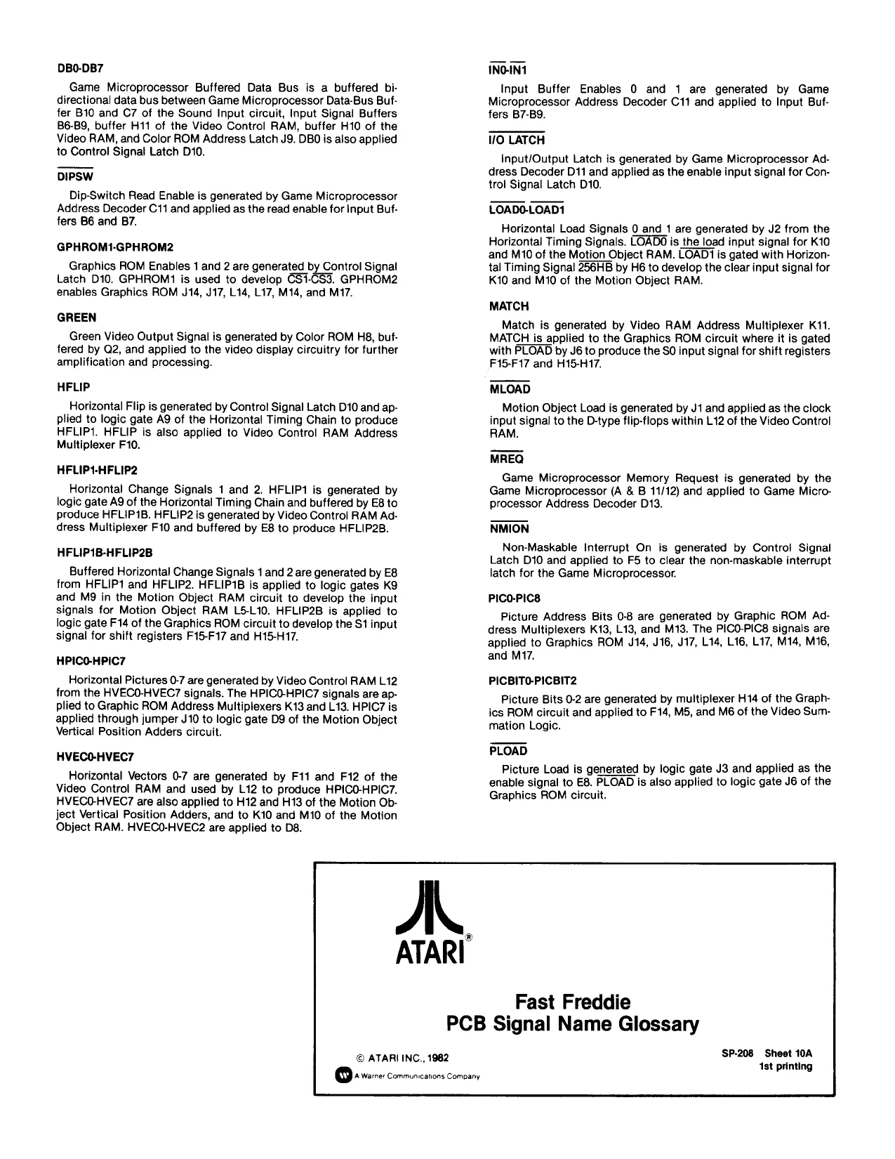
DBO-DB7 Game Microprocessor Buffered Data Bus is a buffered bidirectional data bus between Game Microprocessor Data-Bus Buffer B10 and C7 of the Sound Input circuit, Input Signal Buffers B6-B9, buffer H11 of the Video Control RAM, buffer H10 of the Video RAM, and Color ROM Address Latch J9. DBO is also applied to Control Signal Latch D10.
DIPSW Dip-Switch Read Enable is generated by Game Microprocessor Address Decoder C11 and applied as the read enable for Input Buffers B6 and B7.
GPHROM1-GPHROM2 Graphics ROM Enables 1 and 2 are generated by Control Signal Latch D10. GPHROM1 is used to develop CS1-CS3. GPHROM2 enables Graphics ROM J14, J17, L14, L17, M14, and M17.
GREEN Green Video Output Signal is generated by Color ROM H8, butfered by Q2, and applied to the video display circuitry for further amplification and processing.
HFLIP Horizontal Flip is generated by Control Signal Latch D10 and applied to logic gate AQ of the Horizontal Timing Chain to produce HFLIP1. HFLIP is also applied to Video Control RAM Address Multiplexer F10.
HFLIP1-HFLIP2 Horizontal Change Signals 1 and 2, HFLIP1 is generated by logic gate A9 of the Horizontal Timing Chain and buffered by E8 to produce HFLIP1B. HFLIP2 is generated by Video Control RAM Address Multiplexer F10 and buffered by E8 to produce HFLIP2B.
HFLIP18-HFLIP2B Buffered Horizontal Change Signals 1 and 2 are generated by E8 from HFLIP1 and HFLIP2. HFLIP1B is applied to logic gates K9 and M9 in the Motion Object RAM circuit to develop the input signals for Motion Object RAM L5-L10. HFLIP2B is applied to logic gate F14 of the Graphics ROM circuit to develop the $1 input signal for shift registers F15-F17 and H15-H17.
HPICO-HPIC7 Horizontal Pictures 0-7 are generated by Video Control RAM L12 from the HVECO-HVEC7 signals. The HPICO-HPIC7 signals are applied to Graphic ROM Address Multiplexers K13 and L13. HPIC7 is applied through jumper J10 to logic gate D9 of the Motion Object Vertical Position Adders circuit.
HVECO-HVEC7 Horizontal Vectors 0-7 are generated by F11 and F12 of the Video Control RAM and used by L12 to produce HPICO-HPIC7. HVECO-HVEC7 are also applied to H12 and H13 of the Motion Object Vertical Position Adders, and to K10 and M10 of the Motion Object RAM. HVECO-HVEC2 are applied to D8.
ATARI
ATARI INC., 1982 INO-INA Input Buffer Enables 0 and 1 are generated by Game Microprocessor Address Decoder C11 and applied to Input Buffers B7-B9.
VO LATCH Input/Output Latch is generated by Game Microprocessor Address Decoder D11 and applied as the enable input signal for Control Signal Latch D10.
LOADO-LOAD1 Horizontal Load Signals 0 and 1 are generated by J2 from the Horizontal Timing Signals. LOADO is the load input signal for K10 and M10 of the Motion Object RAM. LOAD1 is gated with Horizontal Timing Signal 256HB by H6 to develop the clear input signal for K10 and M10 of the Motion Object RAM.
MATCH Match is generated by Video RAM Address Multiplexer K11. MATCH is applied to the Graphics ROM circuit where it is gated with PLOAD by J6 to produce the S0 input signal for shift registers F15-F17 and HIS-H17.
MLOAD Motion Object Load is generated by J1 and applied as the clock input signal to the D-type flip-flops within L12 of the Video Control RAM.
MREQ Game Microprocessor Memory Request is generated by the Game Microprocessor (A & B 11/12) and applied to Game Microprocessor Address Decoder D13.
NMION Non-Maskable Interrupt On is generated by Control Signal Latch D10 and applied to F5 to clear the non-maskable interrupt latch for the Game Microprocessor.
PICO-PIC8 Picture Address Bits 0-8 are generated by Graphic ROM Address Multiplexers K13, L13, and M13. The PICO-PIC8 signals are applied to Graphics ROM J14, J16, J17, L14, L16, L17, M14, M16, and M17.
PICBITO-PICBIT2 Picture Bits 0-2 are generated by multiplexer H14 of the Graphics ROM circuit and applied to F14, M5, and M6 of the Video Summation Logic.
PLOAD Picture Load is generated by logic gate J3 and applied as the enable signal to E8. PLOAD is also applied to logic gate J6 of the Graphics ROM circuit.
Fast Freddie
PCB Signal Name Glossary
SP.208 Sheet 10A ‘st printing
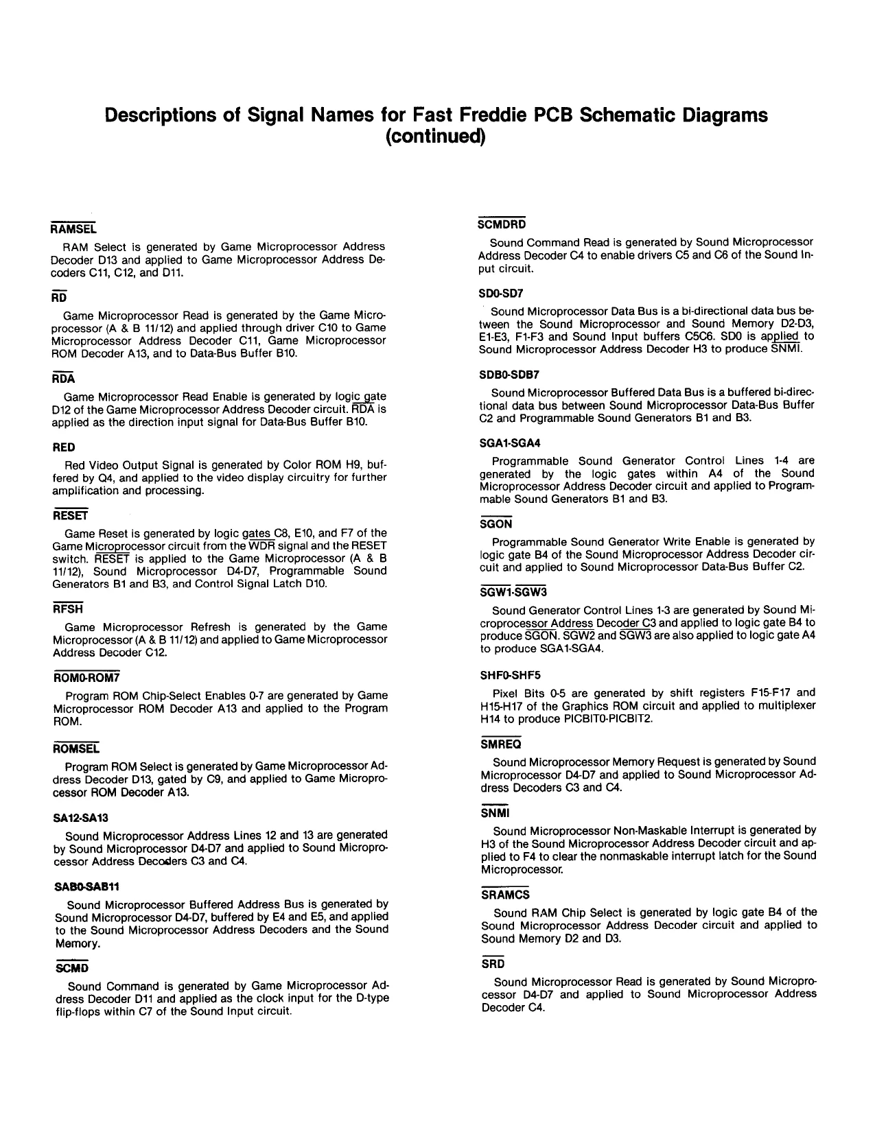
Descriptions of Signal Names for Fast Freddie PCB Schematic Diagrams
(continued)
RAMSEL RAM Select is generated by Game Microprocessor Address Decoder D13 and applied to Game Microprocessor Address Decoders C11, C12, and D11.
RD Game Microprocessor Read is generated by the Game Microprocessor (A & B 11/12) and applied through driver C10 to Game Microprocessor Address Decoder C11, Game Microprocessor ROM Decoder A13, and to Data-Bus Buffer B10.
RDA Game Microprocessor Read Enable is generated by logic gate D12 of the Game Microprocessor Address Decoder circuit. is applied as the direction input signal for Data-Bus Buffer B10.
RED Red Video Output Signal is generated by Color ROM H8, buffered by Q4, and applied to the video display circuitry for further amplification and processing.
RESET Game Reset is generated by logic gates C8, E10, and F7 of the Game Microprocessor circuit from the WDR signal and the RESET switch. RESET is applied to the Game Microprocessor (A & B 11/12), Sound Microprocessor D4-D7, Programmable Sound Generators B1 and B3, and Control Signal Latch D10.
RFSH Game Microprocessor Refresh is generated by the Game Microprocessor (A & B 11/12) and applied to Game Microprocessor Address Decoder C12.
ROMO-ROM7 Program ROM Chip-Select Enables 0-7 are generated by Game Microprocessor ROM Decoder A13 and applied to the Program ROM.
ROMSEL Program ROM Select is generated by Game Microprocessor Address Decoder D13, gated by C9, and applied to Game Microprocessor ROM Decoder A13.
SA12-SA13 Sound Microprocessor Address Lines 12 and 13 are generated by Sound Microprocessor D4-D7 and applied to Sound Microprocessor Address Decoders C3 and C4.
SABO-SAB11 Sound Microprocessor Buffered Address Bus is generated by Sound Microprocessor D4-D7, buffered by E4 and £5, and applied to the Sound Microprocessor Address Decoders and the Sound Memory.
SCMD Sound Command is generated by Game Microprocessor Address Decoder D11 and applied as the clock input for the D-type flip-flops within C7 of the Sound Input circuit. SCMDRD Sound Command Read is generated by Sound Microprocessor Address Decoder C4 to enable drivers C5 and C6 of the Sound input circuit.
SDO0-SD7 Sound Microprocessor Data Bus is a bi-directional data bus between the Sound Microprocessor and Sound Memory D2-D3, £1-£3, F1-F3 and Sound Input buffers C5C6. SDO is applied to Sound Microprocessor Address Decoder H3 to produce SNMI.
SDBO-SDB7 Sound Microprocessor Buffered Data Bus is a buffered bi-directional data bus between Sound Microprocessor Data-Bus Buffer C2 and Programmable Sound Generators B1 and B3.
SGA1-SGA4 Programmable Sound Generator Control Lines 1-4 are generated by the logic gates within A4 of the Sound Microprocessor Address Decoder circuit and applied to Programmable Sound Generators B1 and 83.
SGON Programmable Sound Generator Write Enable is generated by logic gate B4 of the Sound Microprocessor Address Decoder circuit and applied to Sound Microprocessor Data-Bus Buffer C2.
SGW1-SGW3 Sound Generator Control Lines 1-3 are generated by Sound Microprocessor Address Decoder C3 and applied to logic gate B4 to produce SGON. SGW2 and SGW3 are also applied to logic gate A4 to produce SGA1-SGA4.
SHFO-SHF5 Pixel Bits 0-5 are generated by shift registers F15-F17 and H15-H17 of the Graphics ROM circuit and applied to multiplexer H14 to produce PICBITO-PICBIT2.
SMREQ Sound Microprocessor Memory Request is generated by Sound Microprocessor D4-D7 and applied to Sound Microprocessor Address Decoders C3 and C4.
SNMI Sound Microprocessor Non-Maskable Interrupt is generated by H3 of the Sound Microprocessor Address Decoder circuit and applied to F4 to clear the nonmaskable interrupt latch for the Sound Microprocessor.
SRAMCS Sound RAM Chip Select is generated by logic gate B4 of the Sound Microprocessor Address Decoder circuit and applied to Sound Memory D2 and D3.
SRD Sound Microprocessor Read is generated by Sound Microprocessor D4-D7 and applied to Sound Microprocessor Address Decoder C4.
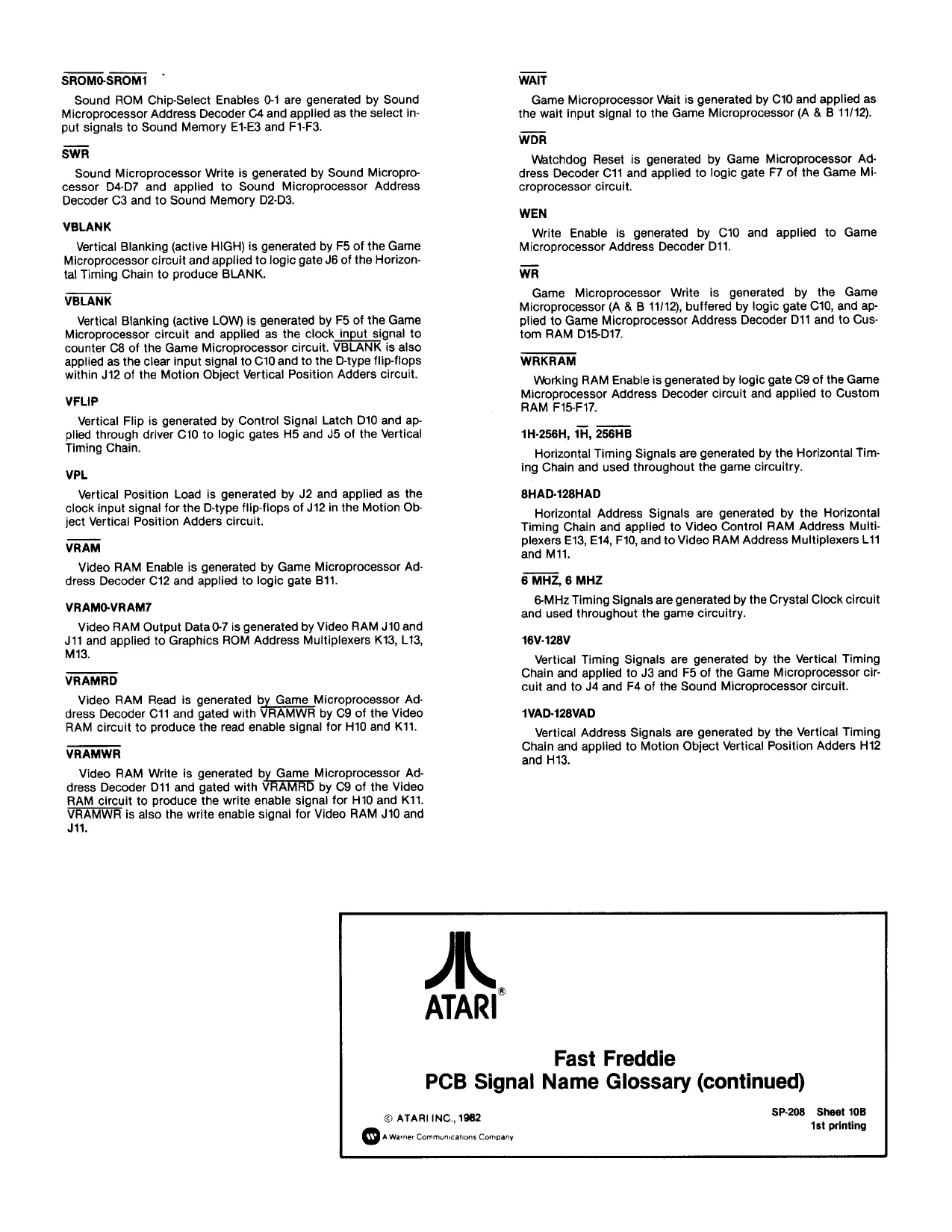
SROMO-SROM1 Sound ROM Chip-Select Enables 0-1 are generated by Sound Microprocessor Address Decoder C4 and applied as the select input signals to Sound Memory E1-E3 and F1-F3.
SWR Sound Microprocessor Write is generated by Sound Microprocessor D4-D7 and applied to Sound Microprocessor Address Decoder C3 and to Sound Memory 02-D3,
VBLANK Vertical Blanking (active HIGH) is generated by F5 of the Game Microprocessor circuit and applied to logic gate J6 of the Horizontal Timing Chain to produce BLANK.
VBLANK Vertical Blanking (active LOW) is generated by F5 of the Game Microprocessor circuit and applied as the clock input signal to counter C8 of the Game Microprocessor circuit. VBLANK is also applied as the clear input signal to C10 and to the D-type flip-flops within J12 of the Motion Object Vertical Position Adders circuit.
VFLIP Vertical Flip is generated by Control Signal Latch D10 and applied through driver C10 to logic gates H5 and J5 of the Vertical Timing Chain.
VPL Vertical Position Load is generated by J2 and applied as the clock input signal for the D-type flip-flops of J12 in the Motion Object Vertical Position Adders circuit.
VRAM Video RAM Enable is generated by Game Microprocessor Address Decoder C12 and applied to logic gate B11.
VRAMO-VRAM7 Video RAM Output Data 0-7 is generated by Video RAM J10 and J11 and applied to Graphics ROM Address Multiplexers K13, L13, M13.
VRAMRD Video RAM Read is generated by Game Microprocessor Address Decoder C11 and gated with VRAMWR by C9 of the Video RAM circuit to produce the read enable signal for H10 and K11.
VRAMWR Video RAM Write is generated GND on Oe orev Address Decoder 011 and gated with VRAI by C9 of the Video RAM circuit to produce the write enable signal for H10 and K11. VRAMWR is also the write enable signal for Video RAM J10 and Jn. WAIT Game Microprocessor Wait is generated by C10 and applied as the wait input signal to the Game Microprocessor (A & B 11/12).
WDR Watchdog Reset is generated by Game Microprocessor Address Decoder C11 and applied to logic gate F7 of the Game Microprocessor circuit.
WEN Write Enable is generated by C10 and applied to Game Microprocessor Address Decoder D11.
wR Game Microprocessor Write is generated by the Game Microprocessor (A & B 11/12), buffered by logic gate C10, and applied to Game Microprocessor Address Decoder D11 and to Custom RAM D15-D17.
WRKRAM Working RAM Enable is generated by logic gate C9 of the Game Microprocessor Address Decoder circuit and applied to Custom RAM F15-F17.
1H-256H, 1H, 256HB Horizontal Timing Signals are generated by the Horizontal Timing Chain and used throughout the game circuitry.
8HAD-128HAD Horizontal Address Signals are generated by the Horizontal Timing Chain and applied to Video Control RAM Address Multiplexers E13, E14, F10, and to Video RAM Address Multiplexers L11 and M11.
6 MHZ, 6 MHZ 6-MHz Timing Signals are generated by the Crystal Clock circuit and used throughout the game circuitry.
16V-128V Vertical Timing Signals are generated by the Vertical Timing Chain and applied to J3 and F5 of the Game Microprocessor circuit and to J4 and F4 of the Sound Microprocessor circuit.
4VAD-128VAD Vertical Address Signals are generated by the Vertical Timing Chain and applied to Motion Object Vertical Position Adders H12 and H13,
ATARI
Fast Freddie
PCB Signal Name Glossary (continued)
© ATARI INC., 1962 SP-208 Sheet 108 ‘Ast printing
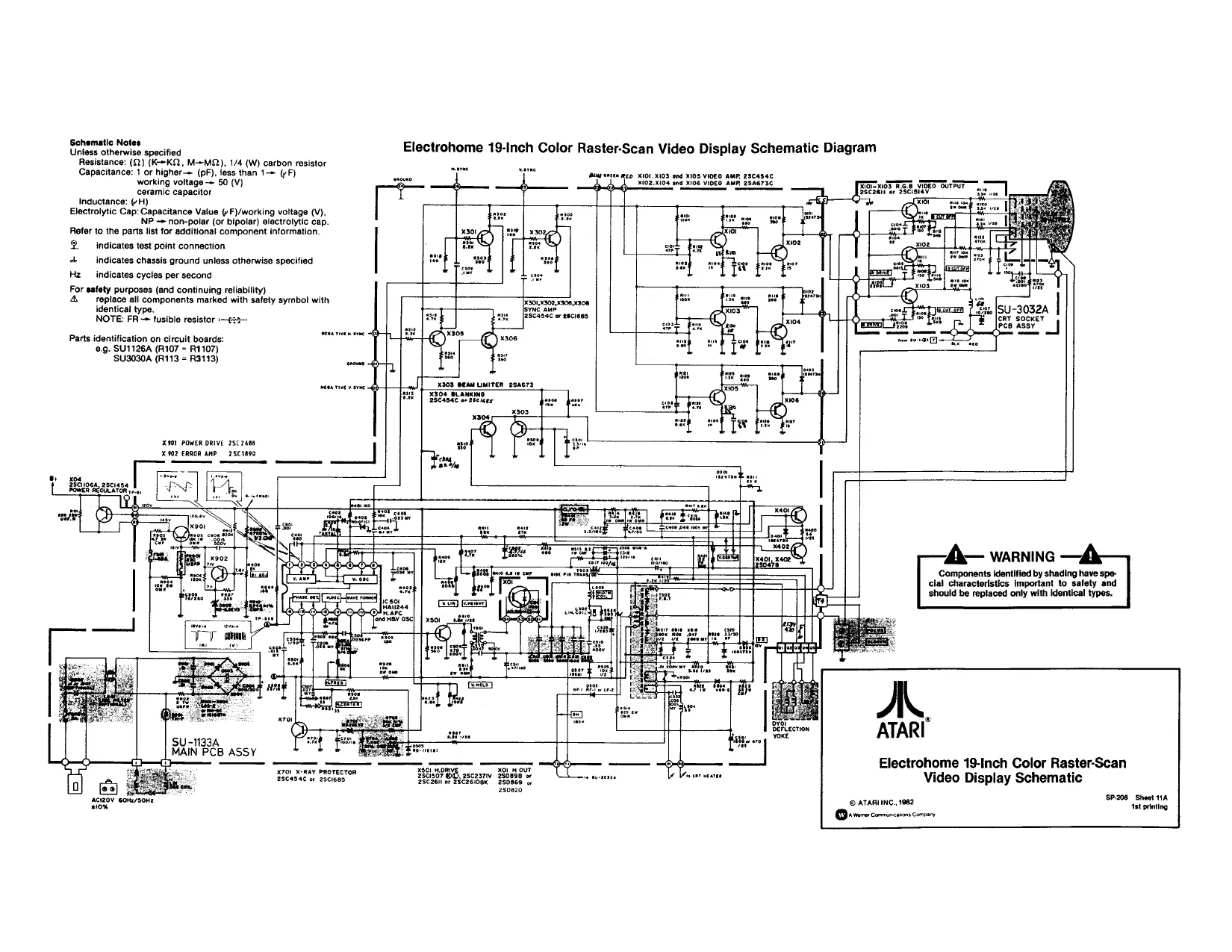
Schematic Notes Unless otherwise specitied Resistance: (<2) (K--K&, M-MQ), 1/4 (W) carbon resistor Capacitance: 1 or higher (pF), less than 1 (/F) working voltage 50 (V) ceramic capacitor Inductance: ¢H) Electrolytic Cap: Capacitance Value F)/working voltage (V), NP - non-polar (or bipolar) electrolytic cap, Refer to the parts list for additional component information. 2 Indicates test point connection + indicates chassis ground unless otherwise specified Hz indicates cycles per second For safety purposes (and continuing reliability) 4 replace all components marked with safety syrnbol with identical type.
Parts identification on circuit boards: saree ‘e.g. SUI126A (R107 = R1107) ‘SU3030A (R113 = R3113)
2901 POWER ORIVE 25¢ 2680, X02 ERROR AMP. 2Sct#90 Electrohome 19-Inch Color Raster-Scan Video Display Schematic Diagram
oe é weeu Nogisiog ond Moe VIDEO AMR SS8GTSE
3013308 730808 leewe a it ocsse wr exciens
aS] aaah oem uusren_enaers ee | age scan taal eee eaeit ae Scolar mz
A— WARNING
lal characteristics should
SU-1133A, MAIN PCB ASSY
"ro, AY Pnorecron BEGPOS, ascosrw Moses oe 2SGdeH or BicaGbue z508ee Identified by shading have spe-
Video Display Schematic
© ATARUING. 1982 Qevwrcomencnn coc Electrohome 19-Inch Color Raster-Scan
'5P.208 Sheet 1A, 1 printing
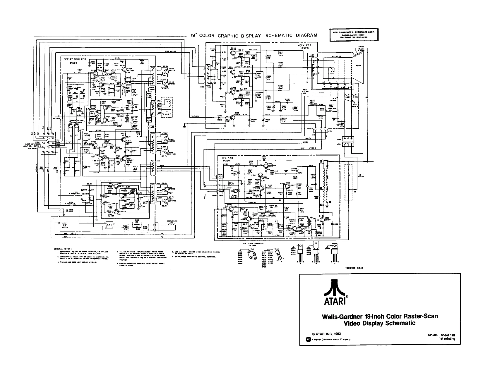
This page is a drawing, shown as the original scan.