Change Lanes
Change Lanes (Taito America Corporation, 1983) · Manual · 76 pages · 20 sections · original scan
\ Berwin
This page carries no recoverable text. It is a drawing or a photograph. See the original scan.

This page is a drawing, shown as the original scan.
Reproduction of this publication is forbidden without the written permission of TAITO
AMERICA CORPORATION, Elk Grove Village, Illinois. This manual is only conditionally
issued, and neither receipt nor possession thereof confers or transfers any right in, or
license to use, the subject matter of the manual or any technical information contained
thereof.
For permission requests, write: TAITO AMERICA CORPORATION 1256 Estes Avenue Elk Grove Village, Iinois 60007 Telephone (312) 981-1000 Telex 25-3290
1.
2.
3. “CHANGE LANES”™ UPRIGHT
TABLE OF CONTENTS
“CHANGE LANES”™ GAME SET-UP............. Page 5 4. ILLUSTRATION & PART LISTS .................--.5 27
1.1 Game Features 0.0.2.0... e eee 6 Figure 1 Fluorescent Panel.................0005 28 1.2 Introduction ....... 2... eee eee ee 6 Figure 2 Back Door Assembly ...............-+ 30 1.3 Game Inspection .................. ee eee eee 7 Figure 3 Control Panel ....... 02... e cece eee eee 32 1.4 Pre-Game Installation .................... 000 7 Figure 4 Steering Wheel Assembly ............. 34 f 1.5 Power On/Off Switch, Self Test Switch, Figure 5 Accelerator Assembly ............-.-4 36 Volume Control, and Service Outlet............. 8 Figure 6 Shift Lever Assembly ...............-+ 38 1.6 Coin Meters ................ 0. sce e eee e eee 8 Figure 7 Coin Door.... 20... ee eee eee eee 40 1.7 Electronic Coin Acceptors ....................5 8 Figure 8 Cabinet Assembly Front View .......... 42 1.8 Test & Alignment Procedure................... 8 Figure 9 Cabinet Assembly Rear View........... 44 MAINTENANCE: «02.02 02-sesesseeeeesteeeeees 7 Figure 10 Optocoupler ...............--.0. 00 46
2.4 Cleaning .......... cc ceceeee eee e eee eeeeee ee 14 Figure 11 Filter Board «0.0.00... 0s eee eee ee 48 2.2 Coin Door ......... 0c eee cece eee 14 Figure 12 Power Supply Component Layout ...... . 50 2.3. Fuse Replacement ...................02.0005 14 Figure 13 Processor Board Component Layout. .... 53,
2.4 Monitor Removal Figure 14 River-Tree PCB Component Layout ..... . 57
2.5 Cover Glass Removal ..............-20--000+ 15 Figure 15 Sound 1/0 Board Component Layout ....61
2.6 Printed Circuit Board Replacement ............. 15 Figure 16 Optocoupler Board Schematic (1 of 1) .. .66
2.7 Power Supply ..........0-.. eee cece e eee ee 15 Figure 17 Power-Supply Schematic (1 of 1) ....... 67 THEORY OF OPERATIONS ..........-...0eeece000- 17 Figure 18 Processor Board Schematic (1 of 3)..... 68
Figure 19 Processor Board Schematic (2 of 3)..... 69 3.1 General...... 2... eee 18 . Figure 20 Processor Board Schematic (3 of 3)..... 70 3.2 Processor Board ........... 0.00 eee eee eee 18 . Figure 21 River-Tree PCB Schematic (1 of 3) ...... 71 3.3 OBJO Generator .......... 02. cece ee eee eee 18 . Figure 22 River-Tree PCB Schematic (2 of 3)...... 72 3.4 Sound 1/0 Board .............-.....0e eee eee 18 , . Figure 23 _—_—River-Tree PCB Schematic (3 of 3)...... 73 3.5 River-Tree Board ......... 0... cece eee eee ee 19 . Figure 24 Sound 1/0 PCB Schematic (1 of 2) ...... 74 3.6 State Machine Operation ... . Figure 25 Sound 1/0 PCB Schematic (2 of 2) ...... 75 3.7. Trouble Shooting .....................0020.8 24 Figure 26 = Wiring Diagram ..................008 76
LIST OF ILLUSTRATIONS
Figure 1-1 Programming Plug..............0.... 7
Figure 1-2 Power ON/OFF Switch ................ 8
Figure 1-3 Self Test Switch ........... 0.00. eee 8
Figure 1-4 Volume Control Setting ............... 7
Figure 1-5 RAM Tests ........... 0. eee ee eee ee ee 9
Figure 1-6 Convergence & Screen Alignment ....... 9
Figure 1-7 Player Controls ...............000008 10
Figure 1-8 DIP Switch Setting .................. 10
Figure 2-1 Coin Door ........ 2... eee eee eee 14
Figure 2-2 Fuse Replacement .................- 14
Figure 2-3 Monitor Removal .................0- 14
Figure 2-4 Cover Glass Removal ................ 15
Figure 2-5 Printed Circuit Boards ............... 15
Figure 2-6 Power Supply .............-..2-0005 15
Figure 2-7 — Current Limit Adjustment ............. 16
Figure 3-1 Timing Diagrams .................04 20
Figure 3-2 Timing Diagrams ................... 21 LIST OF TABLES
Table 1-1
Table 1-2
Table 1-3
Table 1-4
Table 2-1
Table 2-2
Table 3-1
Table 3-2
Table 3-3
Table 3-4 Processor ROM Checksum Test ......... 8
RAM Tests ............. 0c cece eee ee 9 Factory Recommended Settings ........ 10
DIP Switch Settings ................05 11
Line Voltage ..............00....0005 15
Secondary Fuses ................2... 16
Processor Address Map .............. 18
State Machine Data Definition ......... . 22 State Machine Bit Definition ........... 22
State Machine Memory Definition ....... 23
Game Set-Up
“CHANGE LANES”™
- GAME SET-UP
1.1 GAME FEATURES TAITO AMERICA CORPORATION’S ‘CHANGE LANES’’™ upright game is housed in a highly serviceable cabinet with many added features. By putting wheels and leg levelers on the cabinet, moving the game from one location to another is made much easier. Alarge security designed cash box has been incorporated into the design of this cabinet. The Control Panel has a polycarbonate overlay, so cigarette marks and mars an easily be wiped clean. This overlay can be replaced if necessary. The Marquee and Coverglass are made of fully Tempered Glass to minimize breakage. The Back Service Door houses all the PC Boards for the system making servicing of the game, if needed, much easier. Lighted Instructions are provided to further enhance the game and attract players, by making the Instructions easier to read. “CHANGE LANES”™ is also equipped with a new sturdy, eliable steering mechanism designed to take the roughest of handling, which means little or no servicing problems. “CHANGE LANES’’™ also has a Self-Test capability making servicing of the game easier which keeps your game up and running with less down time.
1.2 INTRODUCTION TAITO AMERICA CORPORATION'S ‘CHANGE LANES’’™ upright game is designed for one or two players. The object of the game is to get as many points as possible by traveling as fast as possible for as long as possible. The player's vehicle can travel on land or water.
1.2.1 SCREEN DESCRIPTION The normal “CHANGE LANES”™ screen will be seen as follows: BONUS AT XXXXXX — which is the score that the player must reach to receive bonus fuel (equivalent to earning a bonus car). After the player reaches this score, bonus fuel is awarded, and a new (higher) bonus level is displayed. MILES TO GO — This box indicates the number of miles to the next checkpoint. The number will decrement as the player moves forward. The amount of remaining fuel and the player’s speed are indicated by the two gauges on the right side of the screen. When the player earns bonus fuel, itis indicated by fuel pumps appearing in the area below the speed indicator. The column of numbers on the left-hand edge of the screen indicates all the numbered checkpoints. When a checkpoint is reached, the corresponding checkpoint number in the column is highlighted by the digit turning red and being put on a white background.
1.2.2 Controls Besides the usual 1 player and 2 player buttons, the “CHANGE LANES’’™ control panel has a gearshift lever and a steering wheel. When the gearshift lever is in the up position the player moves forward, and in the down position, the player moves in reverse. The steering wheel controls the left/right motion of the players vehicle. The accelerator (at the bottom of the cabinet) has 3 speed ranges. When the pedal is all the way up, the vehicle is at low speed, halfway down is medium speed and all the way down is full speed.
1.2.3 ATTRACT MODE In the attract mode, the game continually runs through it’s various features. At the start of the attract mode, the vehicle is driving in the gray lanes and on the the river to reach checkpoint #1. When the checkpoint is reached, the car gets refueled, and the first checkpoint indicator is lit. The vehicle then proceeds to the next (second) checkpoint by avoiding the pylons. At the second chckpoint, the car again is refueled and the second checkpoint indicator is lit. On the way to the third checkpoint, the vehicle changes lanes to get to the brown lanes (highest speed lanes). It then drives into the river and reaches the next checkpoint. Note that this checkpoint is just a checkerboard pattern instead of a number. This means that the player did not reach the true checkpoint #3, and therefore does not get a checkpoint bonus. The vehicle will still get refueled, and the third checkpoint indicator will still be lit. The player then proceeds, on the river, to the fourth checkpoint. On the way, a plane passes over and drops a surface missle which hits and destroys the vehicle. The attract mode ends by displaying the high score list, including the “Supreme King of the World.” Note, the high scores are not permanently saved, so that when the game is powered down or put in self-test mode, the current high scores are lost. When there are no credits in the machine, the player may read the on screen instructions (4 pages) by pressing the 1 player or 2 player button. The instructions are also displayed when the steering wheel is spun back and forth a couple of times. 1.2.4 PLAY MODE After the player inserts the required number of tokens/coins, the number of credits bought is displayed in the lower right corner of the screen. The game will continue in the attract mode until the 1 player or 2 player button is pressed. When the 1 player or 2 player button is pressed, the game begins. The player's vehicle is refueled, the message “Drive to Checkpoint 1 before fuel runs out’’ is displayed. On the way to the first checkpoint, the player may decide to drive into the river or stay onthe road. When the player is driving on river, the blimp overhead will drop boxes worth 5,000 points. If the player hits these boxes with his vehicle, he collects the 5,000 points. The player should avoid hitting the sides of the roadway, other cars, and the bomb damage, as these will slow him down and cause him to lose bonus points. The true checkpoint 1 is located on the road. When the checkpoint is reached, the vehicle is refueled, and the amount of time the player took to reach the checkpoint is displayed. The player also earns 100 points for each unit of unused fuel, and the first checkpoint indicator is lit. If the player arrived at the true checkpoint 1, bonus points are awarded according to the players skill: “Ace” awards 50,000 points. Great’ awards 40,000 points. “Good” awards 30,000 points. @ ‘Fair’ awards 20,000 points.
The player then drives to the next checkpoint. A message on the screen tells the player where the next checkpoint is, e.g. ‘‘Drive around pylons for checkpoint 2."" The player may move into the river or over to other lanes.When the checkpoint is reached, the same sequence of events occur as at the first checkpoint. In later screens, the plane passing overhead drops surface missles at the player. If the player is hit, the game is over, unless he has earned bonus fuel. If the player does have bonus fuel, he is awarded with another vehicle (at the cost of his bonus fuel), and _ play continues. While driving on the river, occasional fuel depots will be seen. If the player hits one of them, he gets a free refueling. On some screens, a green car will appear on the screen. During the time it is on the screen, bonus points are constantly accumulated (shown in the box below the the players score). The points stop accumulating when the player hits some object or the car leaves the screen. The player continues on in the above manner until all 9 checkpoints have been reached. At the 9th checkpoint, the player must enter his name as ‘‘King of the World,”’ after which, the game continues.
HIGH SCORE REGISTRATION The player can enter three initials if his score is in the top ten high scores. If the player makes it to the ninth checkpoint, he can enter his full name and it will be displayed as ‘King of the World.” The operator has the option of disabling full name registration completely or reducing it to three letters via DIP switch settings.
1.3 GAME INSPECTION TAITO AMERICA CORPORATION'S “CHANGE LANES’’™ upright game is shipped ready for operation, but a last visual check should be made to insure the game is in good condition. Please verify the following before turning the game on. Check the exterior of the game for shipping damage, chips, dents, or broken parts. © Open the Rear Service Door and check for any interior damage.
© Make sure there isn’t any damage to the wiring. @ Check Printed Circuit Boards, making sure there is no damage to the components. Check fuses making sure they are firmly in their holders. Check for loose foreign objects, especially metal objects which may cause electrical problems. Check Plug-in Connectors making sure they are firmly in their sockets. @ Check the Coin Door for any possible damage, especially the switches.
The Video Monitor is properly adjusted before shipping. If there are any adjustments necessary, refer to our Video Monitor Manual (72-00035-001) This Manual contains all the Manufacturers recommendations for adjusting the Video Monitor.
The RFI (Radio Frequency Interference) shield (a black plastic shield covering the PCB set) must always be in place when the game is operating to prevent interferences to other radio services. 1.4 PRE-GAME INSTALLATION The following precautions should be followed when installing the game.
Avoid rough handling of the game, the picture tube is fragile. @ Install the game on a level surface. © Avoid installing the game where it may receive excessive sunlight or heat, to protect the game from rising internal temperatures. © Do not install in a damp or dusty location. @ For a short time after connecting the power to the game, the picture may be temporarily distorted.
The monitor's purity is affected by the earth’s magnetic field, causing a variation of color. By turning the game on for 10 or 15 seconds and then off for 20 to 30 minutes the automatic degaussing circuit applies a degaussing field around the edges of the monitor. Doing this several times will correct the problem. Another way to correct this problem is to purchase a degaussing coil or buik tape eraser at any electronics store. This will help to immediately demagnetize the Video tube. If you move the game to another location after degaussing the problem may reappear. Refer to Monitor Manual (72-00035-001) for details.
1.4.1 POWER REQUIRMENTS TAITO AMERICA CORPORATION’S ‘‘CHANGE LANES’’™ game is shipped ready for operation at 120 or 240VAC, 60Hz with a power consumption of approximately 250 Watts. The following line voltages may be selected:
100VAC +10% 50/60Hz 120VAC +10% 50/60Hz 200VAC +10% 50/60Hz 220VAC +10% 50/60Hz 240VAC +10% 50/60Hz
A Voltage Pregramming Block is located on the primary side of the Transformer to compensate for high/low conditions. (See Figure 1-1).
FIGURE 1-1 PROGRAMING PLUG
1.5 POWER ON/OFF SWITCH, SELF TEST SWITCH, VOLUME CONTROL, AND SERVICE OUTLET To minimize the hazard of electrical shock while servicing the game a Power ON/OFF Switch is provided. One Self Test Switch, two Volume Controls and a Service Outlet have also been provided. (See Figures 5 and 6 for the location of Switches).
1.5.1 POWER ON/OFF SWITCH, INTERLOCK SWITCH A Power ON/OFF Switch is located in the rear of the game at the top right hand side of the cabinet.
on t
O% 6
FIGURE 1-2 POWER ON/OFF SWITCH
1.5.2 SELF TEST SWITCH There is one (1) Self Test Switch which has (2) positions located on the inside of Coin Door (See Figure 1-4). The ‘CHANGE LANES’”™ game is capable of testing itself and provides data to demonstrate that the games circuitry is working properly.* For further information on the Self Test Procedure refer to Figure 1-7 and Section 1.8.
- The free game position puts a credit on the game without increasing the coin counter.
TEST
FREE GAME © o
FIGURE 1-3 SELF TEST SWITCH
1.5.3 VOLUME CONTROL SETTING There are two (2) Volume Controls both are located on the Sound/ 1.0. Board 08-00109-001. Volume two controls the main overall game sound and Volume one controls the balance between the background and the game volume. We have also included a Volume Control on the inside of the Coin Door. See Figure 1-5 for position. The volume increases when turned clockwise as indicated. /~ (iP
MAIN ~AL ~aAN BALANCE
FIGURE 1-4 VOLUME CONTROL SETTINGS
1.5.4 SERVICE OUTLET A Power Recepatacle has been provided to further aid servicing. The voltage at this receptacle will be the same as the line voltage the game is set at.
1.6 COIN METERS This game is equipped with a Coin Meter.
1.7 ELECTRONIC COIN ACCEPTORS This game is equipped with the capability of using 12VDC Electronic Coin Acceptors, such as Third Wave Electronics, Model TW12 or equivalent. Power for these units may be obtained from the Coin Entry Lamp terminals which provide 12VDC.
1.8 TEST & ALIGNMENT PROCEDURE
1.8.1 GENERAL The Self Test Procedure is performed using the switch located on the inside of the Coin Door. Pushing the test button on the inside of the Coin Door will cause the game to enter the test mode. Once the test mode is entered, all RAM data will be lost including the high scores and any remaining credits. Pushing any button during the test will cause the machine to leave the test. These tests are performed in the following order: © Processor ROM Checksum Test @ RAM test e Player Control Test & Coin Switch Setup Game Mode Setup Convergence and Screen Alignment @ Watchdog Test 1.8.2 PROCESSOR ROM CHECKSUM TEST The five (5) ROM’s are tested and the results displayed on the screen with white characters on a black background. If a failure is detected, the failure is highlighted with red characters on a white background. The left most character in the highlighted area identifies the failed: ROM.
CHARACTERS ROM LOCATIONS Oor1 U25 - Processor Board 20r3 U24 - Processor Board 4or5 U23 - Processor Board 6or7 U22 - Processor Board B U27 - Processor Board
TABLE 1-1 PROCESSOR ROM CHECKSUM TEST
1.8.3 RAM TESTS The five (5) game RAM’s are tested and a good/bad indication is put on the screen. Each RAM takes approximately 7 seconds to test. At the end of approximately 35 seconds, any failed RAM will be indicated.
| RAM 1 | Screen RAM | U31 | | Processor Board | |
| RAM 2 | | Processor RAM | U26 | | Processor Board |
| RAM 3 | | Object RAM | U62 | ‘| Processor Board |
| RAM 4 | | River Bed RAM | U109 | River Tree Board |
RAM 5 | Tree RAM U114 | River Tree Board
TABLE 1-2 RAM TEST
FIGURE 1-5 RAM TEST
1.8.4 CONVERGENCE AND SCREEN ALIGNMENT The grid of white lines is used to detect and correct any convergence problems in the monitor. They are also used to adjust the size and linearity. Adjust the monitor such that the outside edge of the white border is slightly within the boundaries of the tube. This adjustment is made on the center of the lines that make up the rectangle, the corners of the rectangle will extend beyond the shadow mask. FIGURE 1-6 CONVERGENCE AND SCREEN ALIGNMENT
1.8.5 COLOR ALIGNMENT The three left vertical color stripes on the screen are blue, green, and red, at minimum intensity. Adjust the red, blue, and green screen controls such that these stripes are just barely visible and of equal intensity. Next, adjust the red and blue drive controls using the next seven stripes as the grey scale.
1.8.6 WATCHDOG TEST Entering this test puts the processor in a loop waiting for the watchdog reset. This reset should occur within % second of entering this test. When the reset occurs, the processor will re-perform the ROM and RAM tests and then enter the attract mode.
1.8.7 PLAYER CONTROLS STEERING WHEEL The left most digit is the direction indicator, the next digit is the counter. Turn the wheel slowly and observe that the direction indicator remains constant (0 for clockwise, 1 for counter clockwise) and that the counter operates smoothly. Then spin the wheel fast and observe that the direction indicator again remains constant. Any flicker whatsoever means that either the steering wheel mechanism is mechanically misaligned or the optical pickups have deteriorated. (See Figure - ). ACCELERATOR SHIFT — This display indicates the 3 positions of the pedal. 0001 — LOW 0200 — MED 0310 — HIGH
Start 2, Start 1, Free, Left Coin, Right Coin are all indicated next on the screen, Dip Switch C selects the number of coins required and the number of credits given for the left and the right coin switches. This is also used to put the game in free play mode. Dip Switch D selects the number of paid credits required to receive a bonus credit. It also selects which coin counter will be used to accumulate the count for each coin slot and the (King of the World) registration.For switch locations refer to Sound 1/0 Board figure.
FIGURE 1-7 PLAYER CONTROLS
FIGURE 1-8 DIP SWITCH SETTINGS
1.8.8 GAME MODE SETUP Dip Switches A & B are used to set up the game operating mode.
1 2 3 4 5 6 7 8 Switch A off | on | on | on | on | on | off | on Switch B on | on | on | off | on | off | on | on Switch C off | on | on | on | off on | on | on Switch D off _| off | on [on on | on | on Jon
TABLE 1-3 FACTORY RECOMMENDED SETTINGS
" TABLE 1-4 DIP SWITCH SETTINGS
ON = Attract Mode
= Sound On
OFF = Attract Mode
= Sound Off
STEERING WHEEL RATIO
OFF ON ON
(Recommended Setting)
ON = Ignore Memory Failures OFF = Loop On Memory Failures Mode OFF = 1 Player Mode
ON = Steering Wheel OFF = Joy Stick ON = Diagnostic On OFF = Diagnostic Off
MAX. BONUS FUELS ON ON = OFF ON = ON OFF =
OFF GAME DIFFICULTY ON ON = Real Easy OFF ON = Easy ON OFF = Med, OFF = Hard TRAFFIC DIFFICULTY ON ON = Real Easy OFF ON = Easy OFF Med. OFF Hard ON = Car Col Enabled OFF = Car Col Disabled
ON OFF = Land Collisions Disabled
Brae RIGHT SLOT CREDITS/UNIT OFF OFF OFF = 7 Credits ON OFF OFF = 6 Credits / RIGHT SLOT On ou oe cicoe COINS/UNIT = 4Cre ; OFF OFF ON = 8 Gredites ON = 1.Coin/Unit ON OFF on = 2 Credits OFF = 2 Coins/Unit
OFF ON ON = 1 Credits ON ON ON = Free Play LEFT SLOT COINS/UNIT ON = 1 Coin/Unit OFF = 2 Coins/Unit
LEFT SLOT CREDITS/UNIT OFF OFF OFF = 7 Credits ON OFF OFF = 6 Credits OFF ON OFF = 5 Credits ON ON OFF = 4 Credits OFF OFF ON = 3 Credits ON OFF ON = 2 Credits OFF ON ON = 1 Credits
ON ON ON “KING OF THE WORLD” CREDITS FOR BONUS Nae OFF OFF =7 |
ON = Right Coin On Left (Top) Counter OFF = Right Coin On Right (Bottom) Counter ON = Left Coin On Left (Top) Counter OFF = Left Coin On Right (Bottom) Counter ON OFF OFF =6 OFF ON OFF =5 ON ON OFF =4 Nor = Long Name ON = Allow Name OFF ON =3 USED OFF = 3 Letter Name | OFF = No Name
OFF ON =2 ON ON =1 ON ON =0
Maintenance
ALL GAMES REQUIRE A CERTAIN AMOUNT OF MAINTENANCE TO KEEP THEM IN
GOOD WORKING ORDER. A PERIODIC CHECK OF THE MECHANICAL CONTROLS WOULD BE BENEFICAL TO THE SUCCESS OF YOUR GAME.
- MAINTENANCE AND REPAIR
2.1 CLEANING The exterior of the game, all metal parts and all plastic parts can be cleaned with a non-abrasive cleanser. Caution should be used when cleaning the glass, a dry cloth can cause scratches and result in a foggy appearance.
2.2 COIN DOOR The Coin Door used in ‘CHANGE LANES’’™ upright game needs little or no maintenance, See Figure 2-1. If desired, a special coin mechanism cleanser, that leaves no residue, can be obtained from your distributor. Refer to the manufacturers documenation if additional information is needed.
FIGURE 2-1 COIN DOOR
‘
2.3 FUSE REPLACEMENT This game contains eight (8) fuses. Seven (7) of these fuses can be found on the.Power Supply Assembly, five (5) are on the PCB and two (2) are on the Power Supply Bracket. One (1) is located at the bracket where the AC line cord comes into the cabinet. See Figure 2-2 for location of these fuses.
FIGURE 2-2 FUSE REPLACEMENT 2.4 MONITOR REMOVAL \f you need to remove the Video Monitor, follow the instructions listed below:
© Disconnect the power from the line voltage. Disconnect the monitor cable connector. e Remove the wire cable clamps. © Take out the two rear side bolts, one on each side of the cabinet and lower monitor to a horizontal position. © Remove the four (4) monitor mounting bolts and disconnect the green ground wire. Slide the Monitor out by pulling the monitor toward you.
It
FIGURE 2-3 MONITOR REMOVAL
The monitor's purity is affected by the earth's magnetic field, causing a variation of color. By turning the game on for 10 or 15 seconds and then off for 20 to 30 minutes the automatic degaussing circuit applies a degaussing field around the edges of the monitor, doing this several times will correct the problem. Another way to correct this problem is to purchase a bulk tape eraser at any electronics store, this will help to immediately de- Mmagnetize the video tube. If you move the game to another location after degaussing the problem may reappear. Refer to Monitor Manual 72-00035-001 for further details.
2.5 COVERGLASS REMOVAL To remove the coverglass follow the instructions listed below: © Open the Coin Door. e Unlock the Control Panel by releasing the two side latches. e Rotate the Control Panel on its hinges as shown in Figure 2-4, e Lift the Coverglass out.
The Coverglass can now be easily removed from the front of the game with no screws. To replace the coverglass simply reverse the above procedure.
FIGURE 2-5 PRINTED CIRCUIT BOARD
2.7 POWER SUPPLY The Power Supply produces all the necessary game voltage requirements. Refer to Figure 2-6 while reading the following circuit description.
FIGURE 2-4 COVER GLASS REMOVAL
2.6 PRINTED CIRCUIT BOARD REPLACEMENT You may wish to remove ‘CHANGE LANES’’™ printed circuit board, Sound/IO PCB (08-00109-001), Processor PCB (08- 00107-001), and River-Tree PCB (08-00108-001) for servicing. Refer to Figure 2-5. The ‘CHANGE LANES’’™ Printed Circuit Boards (PCB) are located on the back inside of the rear service door for easy access.
- Turn the power switch off and disconnect power cord.
- Open the rear service door. Remove the eleven (11) nuts holding the shield in place. Carefully remove shield for access to the board set.
- Disconnect the connectors from the boards. Disconnect , 7 the ribbon cable connecting the boards by spreading eject FIGURE 2-6 POWER SUPPLY
latches on the connector. ; 2.7.1 AC INPUT
- Loosen and turn the Stop Bracket and slide the boards The AC Input is applied to the main Power Supply via the AC Line toward you out of the board guides. Cords, Line Filter, Line Fuse, Power Switch and Interlock Switch. Different Line Cord are used for 120V and for 240V. The Line Fuse is located on the Line Cords Assembly near the Strain Relief. A Voltage Programming Block is located on the primary side of the Transformer to compensate for high/low voltage conditions. The following line voltages may be inserting the appropriate
| PART 15 OF FCC RULES FOR A CLASS A COMPUTING DEVICE. | Line Voltage | Line Fuse |
| OPERATION OF THIS EQUIPMENT IN A RESIDENTIAL AREA MAY | 100 VAC = 10% | 50/60Hz | 3 AMP |
| CAUSE UNACCEPTABLE INTERFERENCE TO RADIO AND T.V. RE- | 120 VAC + 10% | 50/60Hz | 3 AMP |
| CEPTION REQUIRING THE OPERATION TO TAKE WHATEVER | 200 VAC + 10% | 50/60Hz | 1.5 AMP |
| STEPS ARE NECESSARY TO CORRECT THE INTERFERENCE. | 220 VAC = 10% | 50/60Hz | 1.5 AMP |
240 VAC + 10% | 50/60Hz 1.5 AMP
TABLE 2-1 LINE VOLTAGE 15
There are five secondary sources. Three of them go to the Regulator PCB providing one +5VDC, +12VDC, —12VDC, and ~5VDC. There is one 6.3VAC and one 120VAC used for the monitor, and in certain models for fluorescent lamp and fan. These secondary fuses are located on the bracket adjacent to the Power Transformer.
Secondary Fuse 120VAC 6.3VAC 2.0AMP SLO-BLO 2.5AMP
TABLE 2-2 SECONDARY FUSES
2.7.2 —5VDC AND —12VDC REGULATORS The AC Input for the negative voltages comes into the Regulator PCB on J1-5 and J1-6 from the transformer. Fuse F3 protects against short circuits. The AC voltage is then full wave rectified by BR3 and filtered by C16. The raw DC is then applied to Reg 1, a three terminal —12V Regulator. The output of this Regualtor is the —12VDC output for the system and is also the input voltage for Reg 2, a —5V Regulator. The output of this Regulator is the —-5VDC for the system. Capacitors C17, C18, C19 are to improve the transient response and stability of the minus voltage regulator. Diodes D8 and D9 provide protection agaists C18 and C19 being shorted through the Regulator. Resistors R34 and R35 provide current limiting for LED’S 3 and 4 which will light when there is some voltage present at the regulation outputs.
2.7.3 +5VDC REGULATOR The AC Input for the +5VDC Regulator circuit comes in on J1-1 and J1-2, via F1 into BR1. BR1 full wave rectifies the AC Input. This raw DC is applied to the collectors of (2) series pass transistors, mounted on the Heat Sink Assembly. The regulation is done by U3, which is a voltage regulator whose output controls the gain of Q5, which in turn controls the gain of the series of pass transistors. The emitter of the series pass transistor return to the Regulators PCB and through R11 and R12, which serve to force current sharing between the series pass devices. The voltage at the output of R11 and R12 are the +5VDC for the system. R16 and R18 are voltage set and current foldback adjustments respectively. These are factory adjusted to 5V + .25V. at 6 AMPS. Q8, D3 and R20 comprise a SCR-Type Crowbar Circuit which will trigger when the DC output voltages rise above 5.8V. Once the SCR fires, the Power Supply has to be turned off to reset the device. R19 is a current limiter for the voltage indicator LED 1. R16 is used to set the output voltage of the Regulator. C8, D2, R13 and O4 delay the start-up of the 5V Regulator to allow the —5VDC Regulator to stabilize first. 2.7.4 +12VDC REGULATOR This circuit is essentially the same as the 5V Regulator described above. The AC current comes in on J1-3 and J1-4, via fuse F2 into BR2. The AC is rectified by BR2 and filtered by C9. The raw DC is fed to a single series pass transistor on the Heat Sink Assembly and also powers the +12V and +5V Regulator. R28 and R25 are voltage set and current foldback and factory adjusted to 12 Volts +.25V at 4 AMPS. D7, Q9, and R31 are SCR Crowbar Circuits which trigger at 13VDC output which causes supply to go into shut down to reset power down and then power up again. There is an RC delay as in the 5V circuit to delay the +12V rise time.
2.7.5 RESET CIRCUIT The reset circuit will output a 2sec active low MRST pulse at J3-14 J4-14 when the power is first turned ON and whenever power fails for more than 35ms. The reset circuitry is comprised of a Dual Timer (556) and a fullwave type optical coupler across an AC secondary. The output of U1 is the input to one half of the 556 which is configured as a missing pulse detector. C1 and R3 determine the time before the output goes active. This is set for about 35ms. When two or more cycles are missing, the output of the first timer triggers the second timer which drives the MRST low for about 2 seconds. The timer constant for the second timer is set by R4 and C6. Power on reset is generated by C4, and R39 and D12 on the trigger input of the second timer. Q3 inverts the signal out of the 556 so it is active low. R7 insures MRST is low while the power is rising.
2.7.6 POWER SUPPLY ADJUSTMENTS VOLTAGE Adjust voltage on +5V and +12V for +5.00V to +5.01V and +12.00V to +12.01V. CURRENT LIMIT Adjust control (5 1, 12 1) counterclockwise until voltage just changes, then turn control clockwise until voltage goes back to original value. With pointer, mark position of arrow on potentiometer then turn control until beginning of 1st notch is aligned with the pointer. On the controls with the Blue Disk turn approximately 30 degrees.
FIGURE 2-7 CURRENT LIMIT ADJUSTMENT
Operation
THIS SECTION PROVIDES A TECHNICAL DESCRIPTION OF THE “CHANGE LANES” GAME. THE GAME ELECTRONICALLY CONSISTS OF PRINTED CIRCUIT BOARDS, POWER SUPPLY, AND SPEAKERS WHICH ARE DESCRIBED IN DETAIL IN THE FOLLOWING TEXT.
- THEORY OF OPERATION
3.1 GENERAL The game consists of three boards. The Processor Board, The River-Tree Board, and the Sound/IO Board. The Processor Board contains the Z80B microprocessor, the program ROM and RAM, the scan counters and sync generator, the screen character generator (OBJ1), the moving object generator (OBJO), and the watchdog timer. The River-Tree Board contains a ROM controlled state machine and the math look-up tables for the generation of the size and position of the ground and trees. The Sound/IO Board contains the sound generators, the voice mixer and output color map, the inputs and outputs for switches and coin counters, and the hardware collision detectors.
3.2 PROCESSOR BOARD All of the timing signals are generated on this board. The 20MHz master clock is generated by the crystal and inverters U8. It is divided by flip flop U9 to produce a 10MHz and 5MHz clock. The 10MHz clock is used only by flip flop U10 to generate the FASTWRT™ signal needed for the OBJ1 generator. The 5MHz clock is used as the main timing signal for the rest of the board. The 5MHz clock is shaped by U8 and Q1 to produce the Z80B clock. The horizontal scan counters U1, U2, U3 are clocked by the 5MHz and produce an active horizontal line of 256 counts (51.2us) and a horizontal blanking of 62 counts (12.4us). It also produces HSYNC, HRESET, 20D, HRD*, and FASTWRT*. Refer to the Timing Diagrams. HSYNC is then used to clock the veritcal counters and produce 224 vertical active lines and 38 vertical blank lines. It also produces VSYNC, VSEG1, VSEGO, and the Z80B interrupts. See timing diagram. The watchdog timer U29 is loaded by any access to the WD0G address E000, and is counted down by VBLANK signals. If for some reason, the processor gets ‘‘lost’; and stops generating accesses to WDOG, after 8 VBLANK times the Q3 output of U29 will go low and cause a reset at the Z80B. OBJ1 generator. This circuit generates all of the fixed objects ‘on the screen such as the right hand border and the scores. It also generates the airplane that pulls the sign across the sky. The characters are stored in ROM U46 and are displayed according to the data written into RAM U31 by the processor. Processor access to this RAM is accomplished through multiplexers U19, U20, U21, and buffer U34. Timing for the access is controlled by the flip flops U42 and U41 which generate the mulitplexer control signal and the WAIT 1 signal when the processor accesses the OBJ1 address tange (9000-97FF). Two bytes of information are stored for each character position in the RAM. The first is actual character designation which is loaded into latch U33. The second byte contains the horizontal shift position and color group for that character. The horizontal shift data goes to U45 where it is added to the horizontal scan count and produces address information used by the output latches U58, U59 and the MUX U57. The 2 color group bits from U32 and the 2 MUX output bits from U57 form the 4 bit value for this object data and are sent to the video mixer on the Sound/lO Board. 3.3 OBJO GENERATOR This circuit generates all the fixed size moving objects such as the clouds, the city, the blimp and the cars. The characters are stored in ROMs U97, U98, U99 and U100. They are displayed according to the data written to RAM U62 by the processor. Processor access to this RAM is accomplished thru multiplexers U60, U61, U63 and buffer U65. Timing for this access is controlled by the flip flops U64 which generates the MUX control signal and the WAITO signal when the processor accesses the OBJO address range (8000- 82FF). For each object to be displayed, there are 4 bytes of data stored in the RAM U62. The first is the rotational value and vertical size of the object, the second is the complement of the vertical position of the object, the third is the actual designation of the object, and the fourth is its horizontal position. During each scan line, just after the end of HRESET, the counter U72 and U73 begin sequentially accessing the data in the RAM. The first byte is stored in latch U70. The second byte is subtracted from the current vertical scan count by U80 and U93. The difference is compared with the Vertical size data by U81 and U94 and the results are latched in U95. If these results are such that the currently accessed object is required to appear on the current vertical scan line, then U74 pin 3 will go low and start the object data cycle. Otherwise, the counters U72 and U73 will continue the search. If the data cycle starts, then the third byte of data is loaded into latch U69 as the object identifier, and the fourth byte is loaded into counters U79 and U92 as the horizontal position of the object. Then the flip flops U82 and counter U83 performs a timing cycle whereby the image data in the ROMS is accessed according to the current scan count and rotational bits (VR, HR) and written to the output RAMs U67 or U68. At the end of the timing cycle, the counters U72 and U73 resume the search for objects on this scan line. The output RAMs U67 and U68 are switched on alternate vertical scan lines between outputting data to the video mixer and being available for writes from the data timing cycle. The read or write address is selected by multiplexers U77, U78, U90, U91. As each RAM is read to the screen, it is automatically erased by gates U54 or U55.
Processor ROM OBJO RAM OBJ1 RAM Color RAM Processor ROM River-Tree RAM River-Tree Status Sound/0 Watchdog Processor RAM
TABLE 3-1 PROCESSOR ADDRESS MAP
3.4 SOUND V/0 BOARD All of the sounds are generated by two General instruments AY3- 8910 sound generator chips U8 and U9. These chips also read the DIP switches. The low frequency sounds are genetated by U9, and shaped by U22. The high frequency sounds are generated by U8 and filtered by components. The balance between the two sound generators is set by VR1 and the overall volume is set by VR2.
The Steering Wheel inputs go to the direction flip flop U33 and the counter U32. The count and direction are read by the processor three U31 approximately every 4 milliseconds. The inputs from the coin door are sent to the encryption processor where they are conditioned before going to the Z80B. All other inputs are read thru multiplexers U45 and U30. Outputs for the coin counters and “yoke-flip” control are generated by U44. The Video mixer consists of latches U11, U13, U14, U12, U15, flip flops U18, U20, U17 and assorted gates. The gates that monitor the inputs of each of the latches are used to determine if a valid object is present. Of so, then the related object flip flop is set. The outputs of the flip flop go to the priority gates and the existing object with the highest priority is enabled on to the Multiplexed Address bus. The priority is in the following order, Highest to Lowest OBJ1 Tree 0 or Tree 1, OBJO River. The priority between TREE O and TREE 1 is decided by flip flops U17. Gates U25 and U26 encode the object type into 2 more bits for the Multiplexed Address Bus. The resultant 6 bits on the MA bus go to the output color RAM address inputs. The data outputs of this RAM are used to generate one of 8 levels of intensity for each of the three colors. This RAM is loaded by the processor thru buffer U36 and gate U37. Hardware collision detection is done by flip flops U42 and U33, and gate U41.
3.5 RIVER-TREE BOARD The River-Tree Board is comprised of 4 sections; the Input Buffers and River Math generator, the River Video generator, the Tree 0 Video generator, and the Tree 1 Video generator. The Input Buffers U1, U2, U3 & U4 take in address and timing from the Processor Board and allow data transfer to and from the Processor Board. The River Math generator functions as follows: During Vertical Reset (V8* from U4/16) the slope address counters U33 and U34 are loaded with the horizon value from U19. When Vertical Reset ends, the counters start incrementing on positive edges of HRD*(U4/5). These counters address the slope ROM, U44 which provides horizontal and vertical size data to the River source bus. A ingn speed state machine also synchronized to HRD*(U73, U87, U88, U89, U101, U102, U103, U104, U115, U116 U117, U118 & U119) directs this data to the River Video generator. The actions of this state machine are shown below. Each of the generators is comprised of a Math Train and an image output section. The first description is for the River generator. The Math Train consists of a 4 bit wide path from the data RAM US9 thru the adder (U60, U75 & U61) thru the address latches and counters (U62, U77, U76, U91 & U92) to the horizontal size generator (U106, U107, U121 & U122). At each CLKTRAIN2 (U104/8) the 4 bit data packets are moved one location down the train. The train is fed by either the slope MUX U45, the adder MUX U61, or the data RAM U59. This data is accepted by the adder input U60 or the address train input U62. The data is also written back into the data RAM US9. The data RAM serves as an accumulator, providing storage from one scan line to the next, of the inputs to and the results of the math process. The function of this math process is to add the size data from the slope ROM to the position data in the data RAM and put it to the address train. The initial values of position are loaded into the River data RAM U59 during vertical reset thru MUX US7, U58 and data buffer U47. This initial value is the position of the River at the lower right corner or the screen. The details of this process are shown in the state machine table. This Math process is run during horizontal reset on every scan line. At the end of each process (the beginning of each scan line), the serial train of address latches and counters will contain the vertical and horizontal addresses of the River Video to be displayed. The horizontal address counter is clocked by the horizontal size generator output U122/5. The frequency of the size generator is determined by the value loaded into U106 during the math process. This value is the start value used by counters U107 & U121. These counters count up until they reach FF’hex and are then reloaded by U42/11 with the start value. If the LSB of the start value (U106/19) is high, then flip flop U122/9 will cause the counters to skip 1 clock every other time it reloads. This allows an apparent 40 MHz resolution in horizontal size with only a 20 MHz clock. The resultant addresses now go to the image output generator. The MSB's of the vertical and horizontal addresses go to the image locator RAM U109 to select the image cell (16 lines by 8 pixels) to be displayed. This data along with the LSB’s of the addresses goes to the image ROM U111 and output shifters U126 & 112. Each pixel is 4 bits deep. The result of this math process is to make the image of each successive scan line (starting from the bottom of the screen) smaller and smaller so as to create the illusion of depth and perspective in the ground terrain. The tree generators (Tree 0 is described here) operate the same as the River generator until a tree start pixel (all 0) is detected by gate U52 and flip flop U56. At this time, Tree on is set (U29/5) and the River source bus is disconnected from the tree generator (U63/1). The tree generator continues to function but no new position or size data is received from the river source bus. Position and size data is now taken from the tree data RAM U79 which contains the values last received from the river source bus. The result of freezing the incremental size values is that the image outputs will be clocked at the fixed rate of the ground terrain at the time of the tree was detected. This makes the tree appear vertical and also forces it to track the ground terrain motion.
3.6 STATE MACHINE OPERATION The State Machine is controlled by counters U101 & U87. These counters are clocked by 20D (U115/6). This is a 20MHz clock that is disabled while HRD* is low. Flip flop U102/8 resynchronizes HRD* to 20D and allows the state machine to start. The state machine counters provide the timing for the basic math clock (U105/2) and the address for the state ROM U88. When the counters reach maximum, U105/3 goes low. After a delay of 2 clocks, U119/5 goes low which allows U102/8 to clock low. This ends the state machine cycle. At this time, counter U116 is enabled and it allows a burst of 16 10MHz clocks to go to the math train. This is needed to flush any remaining invalid data from the image outputs. While the state machine is on, the data from the state ROM is latched in U89. This data controls the generation of the various clocks and enables in the various sections of the math train. The details of this operation are shown in the table below.
PROCESSOR CLOCKS FIGURE 3-1
HORIZONTAL BLANKING TIMING “| tore
20 MHz
10 MHz
5 MHz
HO
HI
FASTWRT*
HO
HI
H2
H3
H4
HS
H6
H7
H8
HSYNC
HRSP*
DELAYED CLOCK TIMING
p50
5MHz i" : : HO (2.5 MHz)
HRST*
HRD*
HSYNC
VERTICAL BLANKING TIMING
>| pe oS Sas
vo UCU in
v2
V3
v4
v5
V6
Ww
v8
VSYNC.
PROCESSOR INTERRUPT TIMING
v5 ia YH LL Ls U
ZINT* Ly H : t >
STATE MACHINE DATA DEFINITION TABLE 3-2
| Bits
| fate | 7654321 0| | Hex | Source | Dest.| Description |
| 0 | 0 }0/0}0}1}1{0];1 | OD | ROM | Adder] NOOP - Data From ROM | |
| 1 | O{O}O;O; 14141 1 | OF | ROM | Train} | LSB Clock Offset - From ROMO-To Train-To RAMO |
| 2 | 041500; 141 oft | 40 | RAM | Adder} NOOP - Clock ROM Addr Counter |
| 3 | ofolrfofafs fifa | oF | ROM | Train} | MSBClock Offset-From ROM1-To Train-To RAM1 |
| 4 | 1 4140/0} 1] 1 [O}1 | CO | RAM | Adder| NOOP - Clock ROM Addr Ctr-Clock RAM Addr Ctr | |
| 5 | 0|0}0j{0}1}1 {141 | OF | ROM | Train} LSB Clock Freq-From ROM2-To Train-To RAM2 | |
| 6 | 0f1/0{0]1}1j0]1 | 4D | RAM | Adder| NOOP - Clock ROM Addr Counter | |
| 7 | 00/4 jO;1}1 4141 | QF | ROM | Train | MSB Clock Freq-From ROM3-To Train-To RAM3 |
| 8 | 141}0]0;0;1jO}1 | CS | RAM | Adder} NOOP - Clock ROM ADDR Ctr-Clock RAM Addr Ctr-Clear Carry | |
| 9 | 0{0}0}0}1]1j0}1 | OD | ROM | Adder| HBUMPO - From ROM4-To Adder-To RAM4 | |
| A | Oj1}1{0]1]1{0]1 | 6D | RAM | Adder| HPOSO - From RAMS5-To Adder-To RAMS5-Clock ROM Addr Ctr | |
| B | 1/141 /0}1]41{1[0 | EE | Adder | Train | HPOSO - From Adder-To Train-To RAM5-Clock Carry-Clock RAM Addr | |
| c | 0 }0}0j0}1]14 |O;1 | OD | ROM | Adder| HBUMP1 - From ROM5-To Adder-To RAM6 | |
| D | Oytf1 fO}4]1jo}1 | 6D | RAM | | Adder] HPOS1 - From ROM7-To Adder-To RAM7-Clock ROM Addr Counter | |
| E | 14141 fOf1}1 fifo | EE | Adder | Train | HPOS1 - From Adder-To Train-To RAM7-Clock Carry-Clock RAM Addr Ctr | |
| F | 0 }0;0{0}1}1jo;1 | OD | ROM | Adder} HBUMP2 - From ROM6-To Adder-To RAM8 | |
| O}1]1{O]1]1jO]1 | 6D | RAM | Adder} HPOS2 - From RAM9-To Adder-To RAM9-Clock ROM Addr Counter | ||
| 141}140}1;1 41,0 | EE | Adder | Train | HPOS2 - From Adder-To Train-To RAM9 Clock Carry-Clock RAM Addr Ctr | ||
| 1 j0}0}0}1/1{0}1 | 8D | ROM | Adder} NOOP-Clock RAM Addr Ctr | 7 | |
| 04|1)0 | [1 | 1j0}1 | 4D | RAM | Adder| NOOP-Clock RAM Addr Ctr | |
| 0 j0}0 A Ojo jOj1 | 01 | ROM | Adder} VBUMPO - From ROM8-To Adder-To RAMC-Clear Carry | ||
| Ojt]1 [o| 1;0j0}1 | 69 | RAM | Adder] VPOSO - From RAMD-To Adder-To RAMD-Clock ROM Addr Ctr | ||
| 1 H 140}1]0]1)0 | EA | Adder | Train | VPOSO - From Adder-To Train-To RAMD-Clock RAM Addr Ctr | ||
| 010}0{0)140{0]1 | 09 | ROM | Adder; VBUMP1 - From ROM9-To Adder-To RAME | |
| O41 {1 {O]110 jO}1 | 69 | RAM | Adder| VPOS1 - From RAMF-To Adder-To RAMF-Clock ROM Addr Ctr | ||
| 14141 fof1jo [140 | EA | Adder | Train | VPOS1 - From Adder-To Train-To RAMF-Clock Carry-Clock RAM Addr Ctr | |
| 0 j0;041/1}0 jO}1 | 19 | ROM" | Adder} VBUMP2 - From ROMA-To Adder-To RAM10-Load HOSC From Train | ||
| 0 41}140}1]0 | 1 | 69 | RAM | ‘Adder| VPOS2 - From RAM11-To Adder-To RAM11-Clock ROM Addr Ctr | |
| 1414104140 | O| | EA | Adder | Train | VPOS2 - From Adder-To Train-To RAM11-Clock Carry-Clock RAM Addr Ctr |
| 0 j0|0j0}1)0 | 1 | 09 | ROM | Adder] VBUMP3 - From ROMB-To Adder-To RAM12 | |
| 0 f141j0}1)0 | 1 r 69 | RAM | Adder| VPOS3 - From RAM13-To Adder-To RAM13-Clock ROM Addr Ctr | |
| 141]140}1{0 | 0 L EA | Adder r Train | vPos3 - From Adder-To Train-To RAM13-Clock Carry-Clock RAM Addr |
STATE MACHINE BIT DEFINITION TABLE 3-3
RAM Address Counter Enable Data Select (1 = RAM Value, 0 = ROM Value) Also Clock ROM Addr Ctr When Leaving ROM Mode RAM Address 0 1 = Load Horizontal OSC 0 = Clear the Carry 1 =H Process, 0 = V Process 1= Destination is Train, 0 = Destination Is Adder 1 = Source is Memory, 0 = Source Is Adder
STATE MACHINE MEMORY DEFINITION TABLE 3-4
RAM CONTENTS ROM CONTENTS | 0 | (SB Clock offset LSB Clock Offset 1_[_MSB Clock Offset MSB Clock Offset
| 2_[ | LB Clock FREQ | LSB Clock FREQ |
3 | MSB Clock FREQ MSB Clock FREQ 4 | HBUMPO HBUMPO 5 | HPoso" HBUMP1 6_|_HBUMPt HBUMP2 7_|_HPost HBUMP3 8 | HBUMP2 VBUMPO 9 | HPos2" VBUMP1
| A_|_ | HBUMP3 | VBUMP2 |
| B | | _HPos3" | VBUMP3 |
c_| veumPo o | vPosor [e_| veumes F_|_ vrosi’ to | vaumP2 11_| veos2* 12_[ veumes 13 | vposs*
*Loaded from preload section of River RAM (AS=0). These values represent the lower right corner of the screen.
TROUBLESHOOTING “CHANGE LANES™”’ with Signature Analysis (SA) Equipment required: Signature Analyzer (e.g. HP5004A) NOP fixture for Z80B (e.g. Kurz-Kasch NOPZ80)
The “CHANGE LANES” PCB set can be broken down into two main parts for the purpose of troubleshooting. The first is the hardwired timing generators (horizontal and vertical scan counters) and the second is the processor and associated logic. Since much of the processor activity is based on inputs from the timing generators, they would be a good place to start looking for trouble. All the timing is derived from a 20 MHz oscillator located on the processor PCB. This signal (20 Mhz) is divided by four (5 Mhz) and used to drive the horizontal and verical scan counters. By the way, a signal name followed by an * denotes an active low signal. These show up on the schematic as signal names with a bar over them.
Horizontal and vertical scan counter signatures:
Setup — CLK = 5M (UB-12), rising edge START = STOP = V8 (U3-10), rising edge
Logic hi = F9A0
HO (U2-14) = 8PFO Ht (U2-13) = 6UBU H2 (U2-12) = 4906 H3 (U2-11) = H90C H4 (U1-14) = F979 H5 (U1-13) = 2HH3 H6 (U1-12) = 9330 H7 (U1-11) = 313U H8 (U3-6) = US7C
Vo (U5-14) = 61HF V4 (U6-14) = PFHH V1 (U5-13) = 846C V5 (U6-13) = 2408 V2 (U5-12) = H6P5 V6 (U6-12) = FOF5 V3 (U5-11) = HH31 V7 (U6-11) = A19U V8 (U3-10) = 3911 ve" (U3-9) = UOCt VSYNC (U17- 5) = ICA3 HSYNC (U18- 6) = 7CFH VSEG1 (U 4- 8) = ADIU VSEGO (U 4-11) = 6P5A HRST* (U49-4) = FCF3
SA Setup: CLK = RD* (U38-21), falling edge. START = STOP = A15 (U38-5), falling edge. Logic hi = 0001
AQ = UUUU A 8 = HC89 A1 = 5555 A 9 = 2H70 A2 = CCCC A10 = HPPO A3 = 7F7F All = 1293 A4 = 5H21 A12 = HAP7 AS = OAFA AG = UPFH AT = 52F8 U25-20 (CS*) = 4POA U24-20 (CS*) = 12U3 U23-20 (CS*) = PCOt U22-20 (CS*) = F2A6
SA setup: CLK = RD* (U38-21), rising edge START = A15, falling edge STOP = A15, rising edge (note we're only testing Q000H - 7FFFH).
Logic hi 755U.
DO = 96F9 D1 = H31C D2 = 9UF7 D3 = P965
OBJECT 1 CIRCUITS CHECK. Object 1 circuits generate the lettering (see Theory of Operation) on the screen. If the game is put into self test, the first thing to come up is the checksum screen. All this lettering is generated by the object 1 circuits, and since the screen doesn’t change with time, it is useful for generating some stable signatures.
SA setup: Game displaying “checksum” screen CLK = 5M (U8-12), rising edge START = STOP = V8 (U3-10), rising edge
Logic hi = F9A0
Object 1 EPROM (U46) address inputs: U46-1 = 463A U46-2 = 463A U46-3 = 463A U46-4 = 463A U46-5 = 463A U46-6 = 463A U46-7 = 463A U46-8 = 463A
Object 1 EPROM data outputs: U46- 9 = 49U3 U46-10 = 209P U46-11 = H3H3 U46-13 = POHA
Outputs of Object 1 mux (U57) U57-3 = HHPO U57-4 = OA75 U57-5 = P39C U57-6 = 2037 U5S7-7 = 0217
The further adventures of OBJ 1 signals PCB). ...(on the Sound/l0
SA setup: set the game display (via self test) to the color bar screen. CLK = U11-7 (OBJ 1 CLK), rising edge START = V8", rising edge STOP = V8", falling edge
Logic hi = U0C1
DO (U11-14) = 4P43 D1 (U11-13) = 4A12 D2 (U11-12) = 8A83 D3 (U11-11) = A006 U 4 8 = AUAH U18- 6 = 2U8P U25-12 = HU3U U 4- 6 = HU3U EN1 (U26-8) = 2U8P EN2 (U26-3) = UOCt MA4 (U35-2) = 0000 MAS (U35-3) = HU3U
With the same setup HS (U36-13) = 6129 CB*(U43-13) = 046C H1 (U8-22) = OPA5 River-Tree PCB SA.
Much of the River & Tree display circuitry is driven by the state machine, U88 (see Theory of Operation). The timing signals generated here are used in several places on the board.
SA setup: CLK = U115-2, falling edge START = STOP = U105-2, rising edge
Logic hi = UFP6.
Latched outputs of state machine: U89-2 = UF6P U89-12 = 3F39 U89-5 = UP6F U89-15 = 0002 U89-6 = O05F U89-16 = U8UF U89-9 = 148C U89-19 = 0088
Outputs of River address bus counter: U73-14 = 0U2F U73-13 = 82HO U73-12 = 007F U73-11 = 83HF Outputs of first counter for math eprom: U18 -14 = 2028 U18 -13 = 18HC U18 -12 = 8433 U18 -11 = 83F0
U119- 5 = 7HAF
Move the SA CLK to U104-8 (CLKTRAIN2),set CLK, START, & STOP for falling edge.
Logic hi =" 59A4
U59 address inputs: U59-1 = 0000 U59- 6 = C87F U59-2 = 59A4 US9- 7 = 6H45 U59-3 = U569 U59- 8 = OPAP U59-4 = UP6F US9-10 = 59A4 U59-5 = 4F50
Math eprom data and address signals (U44)
SA setup: CLK = U4-5, rising edge START = V8", falling edge STOP = V8", rising edge Game set on “checksum” screen
Logic hi = 5456
U44-13 = 5456 U44-14 = 2A2C U44-15 = 2A2C U44-16 = 2A2C U44-17 = 5456 U44-23 = 2A2C U44- 1 = 2A2C U44- 2 = 2A2C U44- 3 = 2A2C U44- 4 = 2A2C U44- 5 = 2A2C U44- 6 = 0000 U44- 7 = 0000 U44- 8 = 0000 U44- 9 = 0000 U44-10 = 5456 U44-11 = 7P7H
U45- 4 = 0000 U45- 7 = 5456 U45- 9 = 5456 U45-12 = 7P7H
Illustration &
Parts Lists
FLUORESCENT PANEL (07-00273-001)
TAITO TEM PART NO. DESCRIPTION 26-00005-001 | Starter Socket, Fluorescent 29-00003-001 | Switch Starter, Fluorescent 42-00147-001 | Light Panel, C.L. { 4 | 27-00001-001 | Lamp, Fluorescent 15W 18-00002-001 | Ballast Transformer 120V 26-00004-001 | Lamp Socket, Fluorescent
FLUORESCENT PANEL (07-00273-001)
BACK DOOR
new | TAITO PART NO. DESCRIPTION 42-00148-001 Back Door 61-00300-001 Ground Plate 08-00114-001 Filter Bd. Assy. 08-00113-001 PCB Set C.L. 63-00140-001 Shield EMI/RFI
59-00057-001 Speed Nut 61-00221-001 Bracket, Lock Rod L-1 61-00246-001 Lock Rod Assy L-1 08-00107-001 Processor PCB
08-00108-001 River-Tree PCB S| Slole|wlola}aleolr|= 08-00109-001 Sound / /0
BACK DOOR
CONTROL PANEL
TAITO ITEM PART NO. DESCRIPTION 63-00139-001 | Steering Wheel 63-00141-001 Shift Ball & Shaft 07-00259-001 Shift Assembly 09-00269-001 Harness 61-00015-001 Strike Hook 29-00016-001 Leaf Switch 54-07001-008 Nut Stamped 56-11 63-00025-001 Switch Support 63-00024-001 Push Button Short White Slololwlafa}alwlr|a 63-00132-001 Lexan Overlay
CONTROL PANEL
STEERING WHEEL ASSEMBLY
TAITO TEM PART NO. DESCRIPTION 61-00299-001 | Drive Shaft 63-00139-001 | Steering Wheel 51-02024-104 | #10-24 Screws Blolm]— 61-00303-001 | Bracket
| | 5 | | | 63-00150-001 | Pulley |
| | 6 | | | 59-00058-001 | Standoff |
51-00014-001 | Shoulder Screw 55-02001-001 | Lockwasher # split 51-02011-002 | Screw #4-40 x % Hex Wshr. Hd. 55-01001-001 | Flat Washer #4 08-00121-001 | Optocoupler P.C. Assy. [12__| _55-02002-001 | Lockwasher #4 Split 51-02012-004 | Screw #6-32 x ¥ Hex Wshr. Hd. 61-00267-001 | Mounting Bracket 54-03007-001 | Locknut %-16 Nylon Insert 55-03007-001 | Lockwasher % External 61-00266-001 | Interrupter Wheel 61-00308-001 | Drive Shaft 19 55-00001-002 | Lockwasher ¥% Internal
| 20 | | | _55-02004-001 | Lockwasher #10 Split |
21 55-01008-001 | Washer 1” 0.D. x % 1.D. x 14GA 62-00007-001 | ‘‘O” Ring 54-00002-001.} Nut #6-32 Kepsnut
STEERING WHEEL ASSEMBLY
ACCELERATOR ASSEMBLY
| 6 | 54-02004-001| | Keps Nut #10-24 |
| 7 | 61-00288-001| | Accelerator Switch Plate |
| 8 | 62-00008-001| | Rubber Bumper |
| 9 | 63-00151-001| | Accelerator Pedal |
| 10 | 61-00287-001| | Pedal Lever |
| 11 | 51-00013-001| | Shoulder Screw |
| 12 | 51-02014-001} | #10-24 x 1” Screw |
| 13 | 55-01004-001| | #10 x % OD Washer |
This page carries no recoverable text. It is a drawing or a photograph. See the original scan.
SHIFT LEVER ASSEMBLY
TAITO | ITEM PART NO. DESCRIPTION 1 99-F90-00288A | Shift Knob 2 99-F90-00557A| Mask 3 99-E10-00380A] Lever 4 99-P06-00021Aj Pan Hd Screw M3 x 6 5 99-P30-00004A} Lock Washer 3M 6 99-P27-00010A| Plain Washer 8M 7 99-E10-00385A] Center Shaft 8 99-P27-00009A) Plain Washer 6M 9 99-P26-00011A] Flange Nut M6 10 99-E30-01470A| Shift Bracket (A) 1 99-E40-00090A| Spring 12 99-P32-00007A]E-Ring ETWJ-4 13 99-P21-00002A] Self Locking Nut 14 99-P29-00008A] Spring Washer 15 99-F10-00381A | Guide Arm 16 99-P21-00002Aj Self Locking Nut 17 | 99-P06-00021A) Pan Hd Screw M3 x 6 18 99-E30-01459A| Spacer 19 99-E30-00153A) Nut Plate 20 99-P15-00032A] Pan Hd Screw Self Tap 21 99-P43-00026A| Bind Hd Screw M3 x 16 22 99-F90-00150A} Insulator V-type 23 99-C02-00083A] Micro Switch AH7155660 24 99-P29-00008A] Spring Washer 5M 25 99-F30-01434A|Cam 26 99-F90-00553A | Rubber Bumper 27 09-00255-001 | Wiring Harness 28 99-E90-00419A] Shift Bracket (B) 29 99-E10-00386A| Oilite Bush
SHIFT LEVER ASSEMBLY
COIN DOOR
TAITO
| ITEM | PART NO. | DESCRIPTION | REFERENCE |
| 1 | 61-00270-001| Door Frame | 15-8039 | |
| 2 | 61-00271-001| Door | 15-8038 | |
| 3 | 61-00273-001| Taito Name Plate | 15-8115 | |
| 4 | 63-00124-001| Coin Entry Slot | 15-8074 | |
| 5 | 63-00125-001| Push Button Cover | 15-8072 | |
| 6 | 63-00126-001 | Push Button | 15-8071 | |
| 7 | 58-00007-001| Compression Spring | 30-7722 | |
| 8 | 63-00127-001 | Reject Lever | 15-8084 | |
| 9 | 61-00274-001} Coin Chute | 15-8075 | |
| 10 | 63-00128-001| Coin Return Door | 15-8083 | |
| 1 | 33-00002-001} Coin Counter 12 V.A.C. | 31-4550 | |
| 12 | 61-00276-001| Guard | 15-8092 | |
| 13 | 23-00003-001 | Coil Assortment | 15-8091 | |
| 14 | 63-00130-001| Switch Cover | 15-8043 | |
| 15 | 29-00036-001| Slam Switch | 15-1255, | |
| 16 | 59-00055-001| Plastic 25* Coin Acceptor | 31-4014 | |
| 17 | 63-00131-001| Coin Acceptor Retainer | 15-8086 | |
| 18 | 59-00020-025} ¥%4" “E" Ring | 30-0731 | |
| 19 | 58-00008-001 } Extension Spring | 30-7372 | |
| 20 | 61-00277-001 | Service Switch Bracket (Switchcraft No. 46311 Mar.) | 15-8030 | |
| 21 | 29-00037-001 | Service Switch | 23-1339 | |
| [2 | 07-00242-001| Lock 54” Assembly | 34-1855 | |
| 23 | 07-00243-001} Lock Cam Assembly | 55-2909 | |
| 24 | 61-00278-001| Lock Cam Plate | 55-2909 | |
| 25 | 61-00279-001| Wire Form (Coin Switch) | 23-1348 | |
| 126 * | 09-00258-001} Door Cable Assembly | 15-0868 |
- Not Shown
COIN DOOR
CABINET ASSEMBLY FRONT VIEW
ITEM TAITO PART NO. DESCRIPTION 07-00273-001 Light Panel Assembly 47-00019-001 Marquee 61-00249-001 Marquee Mounting Bracket 47-00021-001 Coverglass 63-00089-001 Shroud 07-00256-001 Control Panel Assembly 59-00008-001 Clamp Latching 41-00022-001 Cabinet 61-00212-001 Volume Control Bracket Slololwlola}alojr 11-60002-502 Volume Control 61-00277-001 Switch Bracket
29-00037-001 Slide, Center Return Switch 07-00276-001 Coin Door
63-00151-001 Accelerator Pedal 27-00006-001 | #47 Bulb 26-00008-001 Socket Lamp
CABINET ASSEMBLY FRONT VIEW
CABINET ASSEMBLY REAR VIEW
{_ TAITO ITEM PART NO. DESCRIPTION 1 61-00221-001 | Lock Rod Bracket 2 07-00083-002 | Speaker Assembly 3 61-00038-001 | Speaker Grill 4 _| 41-00022-001 | Finished Cabinet 5 07M00042-001} A/C Line Cord Assembly 6 07-00258-001 | Accelerator Assembly 7 07-00275-001 | Regulator Assembly 8 | 61C00054-001 | Cash Box Lid Q 61D00060-001 | Cash Box 10 61B00039-001 | Cash Tray Handle 1 63R00010-001 | Cash Tray Only 12 63-00019-001 | Cash Tray Separator 13 07M00054-001| Cash Tray Assembly 14 42C00013-001 | Monitor Support Cleat 15 61D00208-011 | Monitor Bracket 16 31-00016-001 | 19” Monitor 17 04-00037-001 | Lock Assembly 18 61-00210-001 | Latch 19 29-00023-001 | Power On-Off Switch 20 63-00140-001 | Shield 21 07-00274-001 | Transformer Assembly 22 07-00041-001 |Heat Sink Assembly
CABINET ASSEMBLY REAR VIEW
OPTOCOUPLER
TAITO ITEM PART NO. DESCRIPTION ul 15-53900-001 | LM3900 0c1 15-60010-001 | Optocoupler oc2 15-60010-001 | Optocoupler C1 12-10001-471 | 470 pf c2 12-30001-475 | 4.7 uf tant. RI 11-00001-513 | 51K R2 11-00001-333 | 33K R3 11-00001-821 | 820 R4 11-00001-513 | 51K R5 11-00001-333 | 33K R6 11-00001-821 | 820 R7 11-00001-105 | 1M R8 11-00001-105 | 1M RQ 11-00001-241 | 240 R10 11-00001-241 | 240 ul 17-00001-001 | Ferrite Bead J 25-00002-005 | 5 Pin Connector (mounted on solder side)
OPTOCOUPLER
[ Gas |
R9 R7 2{|[2 am
Cc ¢ , oc ba 2 @ oI | ae) RIO R8 °° fe) A “
- a(| [la
Ll al | [|e
FILTER BOARD
TAITO PART NO. [nescrarncn QUANTITY
12-10003-471 Cap, 470pf + 10% Axial Lead 17-00001-001 Ferrite Bead Assembly 25-00002-014 Connector 14P
25-00002-005 Connector 5P 14-23904-001 Transistor NPN 2N3904 11-00001-102 Resistor 1K ohm YW 11-00001-332 Resistor 3.3 ohm %4W 63B00068-001 Stand Off 17-00002-001 Ferrite Bead Assembly 17-10001-001 Inductor, 10H
000°
O A
v7 OOCCLO FILTER BOARD
[1_conn, 5 PIN
i
SE ws6t Oni
FERRITE BEADS co exo ceaLen
oeocncnnn can sia TCT Oy oh oo Ib 0 000 CON000CCCO
TRANSISTOR oCjm RESISTOR fF — resistor Juz
0000 = : |< conn 14P i) 1A tA
ow RESISTOR
gig OOOO 60 don
oy 100 90000 2¢ cana)
POWER SUPPLY COMPONENT LAYOUT
ie. & | : > om feral ae oS
10a LeDa|
co 08-00007-001 iss.¢
MADE IN US.A,
BRS + bs) v3, v4
© iva an
4A
onl
POWER SUPPLY
| TAITO | , | TAITO | |
| SYM | PART NO. | DESCRIPTION | ‘SYM | PART NO. | DESCRIPTION |
| R1_[11-00001-102 | Resistor 1.0K 5% YW 5% | C5_{ | 12-10001-102 | Capacitor, .001uf | |
| R2 | 11-00001-512 | Resistor 5.1K YaW 5% | C6 | 12-30001-106 | Capacitor, Tantalum 10uf | |
| R3_| | 11-00001-183 | Resistor 18K %W 5% | C7 __| 12-20003-509 | Capacitor, Electrolytic 50,000ut | |
| R4 | 11-00001-224 | Resistor 220K YW 5% | C8_| | 12-30001-105 | Capacitor, Tantalum 1.uf 35V | |
| RS__| | 11-00001-020 | Resistor 2ohm YW + 5% | C9 | 12-20003-209 | Capacitor, Electrolytic 20,000uf | |
| R6__| | 11-00001-222 | Resistor 2.2K %W 5% | C10 | 12-10001-332 | Capacitor, Ceramic .0033uf |
R7__ | 11-10001-101 | Resistor 100K %4W 5% C11 | 12-30001-476 | Capacitor, Tantalum 47uf R8 | 11-00001-102 | Resistor 10K %4W 5% C12 | 12-30001-105 | Capacitor, Tantalum 1.uf 35V
| RQ__| | 11-00001-472 | Resistor 4.7K YW 5% | C13 | 12-10004-103 | Capacitor, Ceramic .O1uf |
| R10_| | 11-10001-101 | Resistor 100K vaW 5% | C14 | 12-10001-102 | Capacitor, .001uf |
R11_|11-30001-015 | Resistor .15 4W 5% 15 | 12-30001-476 | Capacitor, Tantalum 47uf R12 [11-30007-078 | Resistor .15 4W 5% C16 | 12-20002-108 | Capacitor, Electrolytic 1,000uf R13 | 11-00001-472 | Resistor 4.7K %aW 5% C17 | 12-30001-225 | Capacitor, Tantalum 2.2uf 25V
| R14_| | 11-00001-222 | Resistor 2.2K %4W 5% | C18 | er Capacitor, Tantalum 2.2uf 25V |
R15 [i1-00007-222 Resistor 2.2K YW 5% C19 | 12-30001-105 | Capacitor, Tantalum 1.uf 35V
| R16 | 11-60001-252 | Pot 2.5K 4W 20% | tal | [z#-00008-010 | 10A Fuse |
| R17_| | 11-00001-222 | Resistor 2.2K %W 5% | F2__ | | 24-00003-010 | 10A Fuse |
| R18 [11-60007-102 Pot 1.0K %4W 20% | F3__ | | 24-00003-003 | Fuse, 2A |
R19 | 11-00001-511 | Resistor 510K %W 5% F4 __ | 24-00003-004 | Fuse, 4A
| R20_| | 11-10001-470 | Resistor 47K YW 5% | F5 | 24-00003-004 | Fuse, 44 | | |
| R21_| | 11-00001-162 | Resistor 1.6K %4W 5% | BR1 | 13-00100-025 | Diode Bridge 25A, 100V | |
| R22_| | 11-00001-103 | Resistor 10K %4W.5% | BR2 | 13-00100-012 | Diode Bridge 12A, 100V | |
| R23 ‘[11-00001-472 | Resistor 4.7K YaW 34 | BR3 pee | Ore Diode Bridge 2A, 100V |
| R24_ | 11-00001-222 | Resistor 2.2K %4W 5% | D1__| | 13-14002-001 } Diode IN4002 | |
| R25_| | 11-60001-102 | Pot 1.0K YW 5% | D2__| | 13-14002-001 | Diode IN4002 |
| R26 [11-00001-472 | Resistor 470K YaW 5% | D3 __| 13-10752-001 | Diode, Zener IN4002 | |
| R27_| | 11-00001-222 | Resistor 2.2K %4W 5% | 04 | 13-14002-001 | Diode IN4002 | |
| R28 | [11-60001-252 | Pot 2.5K YaW 20% | D5 | 13-14002-001 | Diode IN4002 | |
| R29 |[11-00007-472 | Resistor 4.7K YaW 5% | D6 | 13-14002-001 | Diode IN4002 | |
| R30_| | 11-00001-122 | Resistor 1.2K YaW 5% | 07 _| 13-10964-001 | Diode, Zener IN4002 | |
| R31_| | 11-10001-470 | Resistor 47K “4W 5% | D8 __| 13-14002-001 | Diode IN4002 | |
| R32_| | 11-30001-015 | Resistor .15K 4W 5% | D9 | 13-14002-001 [Diode IN4002 | |
| R33_| | 11-00001-222 | Resistor 2.2K YW 5% | D10_ | 13-14002-001 | Diode IN4002 | |
| R34_| | 11-00001-122 | Resistor 1.2K %W 5% | D11_ | 13-14002-001 | Diode IN4002 | |
| R35_|11-00001-511 | Resistor 510 YW 5% | D12_| | 13-14002-001 | Diode IN4002 | |
| R36_ | 11-00001-222 | Resistor 2.2K %4W 5% | D13_| | 13-16276-001 | Transorb (IN6276) |
R37 | 11-00001-104 [Resistor 100K 014 | 13-16281-001 | Transorb (IN6281) R38 _| 11-00001-103 | Resistor 10K %4W 5% D15_ | 13-14002-001 | Diode IN4002
| R39_| | 11-00001-224 | Resistor 220L %4W 5% | D16 | 13-14002-001 | Diode IN4002 | _| |
| C1 | 12-30001-225 | Capacitor, Tantalum 2.2uf 25V | | | D17 | 13-16267-001 | Transorb (IN6267) |
C2 | 12-10004-103 | Capacitor, Ceramic .Otuf LED1 | 13-00001-001 | LED (Red) [os] 12-10004-103 | Capacitor, Ceramic .O1uf LED2 | 13-00001-001 | LED (Red)
| C4 | 12-30001-105 | Capacitor, Tantalum 1.uf 35V | LED3 | 13-00001-001 | LED (Red) |
LED4 13-00001-001 | LED (Red)
POWER SUPPLY
TAITO SYM | PART NO. DESCRIPTION U1 | 15-62500-001 | Opto Coupler H11AA2 U2__|15-50556-001 | Timer (Dual) 556 U3 | 15-50723-001 | Voltage Regulator 723 U4 | 15-50723-001 | Voltage Regualtor 723 REG1 | 15-57912-001 | Voltage Regualtor 7912 REG2 | 15-57905-001 | Voltage Regualtor 79L05 Q1 | 14-22905-001 | Transistor 2N2905 Q2 | 14-22905-001 | Transistor 2N2905 Q3 | 14-22905-001 | Transistor 2N2905 Q4 | 14-22905-001 | Transistor 2N2905 Q5 _| 14-23055-001 | Transistor 2N3055 Q6 | 14-22905-001 | Transistor 2N2905 Q7 | 14-20030-001 | Transistor TIP-30A Q8 | 14-26401-001 | SCR 2N6401 Q9 | 14-26401-001 | SCR 2N6401 J1 | 25-00022-006 | Connector, 1-380999-0 6Pin J2__|25-00022-008 | Connector, 350212-1 8Pin 33 |25-00002-014 | Connector, 09-60-1141 14Pin J4 — |25-00002-014 | Connector, 09-60-1140 14Pin 24-10001-001 | Fuse Clips 30-00220-002 Heat Sink Dual To-220 30-00003-001 | Heat Sink Single To-3
PROCESSOR BOARD COMPONENT LAYOUT
a 3, [F
3 6 i 29 7 ear
as ws use
Oks
we (] oD 22 3
wee Woe ehh ves ni ey Pe 3] o/| | lO] Bi Ig 3 5 Fy a) a ik Cc re s 7 us eu ou us al ca SC
ol aljo 1]
ang 0 3 gle 8 fen 2B . ee
PROCESSOR BOARD
TAITO TAITO
| ITEM | PART NO. | DESCRIPTION | ITEM | PART NO. | DESCRIPTION | |
| U1 | 15-70163-001 | 748163 4 Bit Counter | U49_ | 15-20004-001 | |74LS04 Inverter Hex | ||
| U2__| | 15-70163-001 | 74S163 4 Bit Counter | USO | 15-20244-001 | |74LS244 Octal Buffer | |
| U3 | 15-20109-001 | 74LS109 Dual JK Flip Flop | US51 | 15-20245-001 | |74LS245 Bus Transceiver | ||
| u4 | 15-20008-001 [741808 Quad 2 Input AND | U52_| | 15-70008-001 | |74S08 Quad 2 input AND Gate | |
| U5 | 15-70163-001 | 745163 4 Bit Counter | U53_}15-70051-001 | |74S51 Dual AND-OR Invert | ||
| U6 _| 15-70163-001 | 745163 4 Bit Counter | US4 | 15-20032-001 | |74LS32 Quad 2 Input OR | ||
| U7 __| 15-20086-001 | 74LS86 Quad 2 Input EXCL | U55 | 15-20032-001 | |74LS32 Quad 2 Input OR | ||
| U8 | 15-70004-001 | 74S04 Hex Inverter | U56 | 15-70020-001 | |74S20 Dual 4-Input NAND | ||
| ug _[15:70114-001 | 748114 Dual JK FF | U57_|15-20153-001 | |74LS153 Multiplexer Dual | |
| U10 | 15-70112-001 | 748112 Dual JK FF | U58 | 15-20670-001 | |74LS670 4x4 Register File | ||
| U11_| | 15-70008-001 | 74S08 Quad 2 Input AND Gate | U59_ | 15-20670-001 | |74LS670 4x4 Register File | |
| U12_ | 15-20244-001 | 74LS244 Qctal Buffer | U60 | 15-20157-001 | |74LS157 Mux Quad 2 Input | ||
| {U13 | 15-20245-001 | 74LS245 Bus Transciever Octal | U61 | 15-20157-001 | |74LS157 Mux Quad 2 Input | |
| U14 | 15-20244-001 | 74LS244 Octal Buffer | U62_|15-10013-001 | |RAM, Static NMOS 2KX8 200NS | ||
| U15 | 15-20244-001 | 74LS244 Octal Buffer | _] | U63_ | 15-20157-001 | |74LS157 Mux Quad 2 Input | |
| U16 | 15-20002-001 | 74LS02 Quad 2 Input NOR | U64 | 15-20175-001 | |74LS175 Quad Flip Flop | ||
| U17_| | 15-20074-001 | 74LS74 Flip Flop Dual D | U65 | 15-20245-001 | |74LS245 Bus Transceiver | |
| U18 | 15-20074-001 | 74LS74 Flip Flop Dual D | U66 | 15-20175-001 | |74LS175 Quad Flip Flop | ||
| U19 | 15-20157-001 | 74LS157 Mux Quad 2 Input | U67 | 15-10020-001 | {256X4 RAM | ||
| U20_ | 15-20157-001 | 74LS157 Mux Quad 2 Input | U68 | 15-10020-001 | {256X4 RAM | ||
| U21_ | 15-20157-001 | 74LS157 Mux Quad 2 Input | U69 | 15-20377-001 | {74LS377 Octal D FF | ||
| U22_| | 16-00026-001 | EPROM Change Lanes | U70_|15-20377-001 | |74LS377 Octal D FF | |
| U23_ | 16-00026-002 | EPROM Change Lanes | U71_ | 15-20139-001 | |74LS139 Dual Decoder | ||
| U24 | 16-00026-003 | EPROM Change Lanes | U72_|15-20161-001 | |74LS161 Counter 4 Bit Preset | ||
| U25_| | 16-00026-004 | EPROM Change Lanes | U73_|15-20161-001 | |74LS161 Counter 4 Bit Preset | |
| U26 | 15-10013-001 | RAM, Static NMOS 2KX8 200NS | U74 | |15-20000-001 | |74LS00 Quad 2 Input NAND | |
| 16-00026-005 |EPROM Change Lanes | U75 | 15-20032-001 | |74LS32 Quad 2 Input OR | ||
| 15-20074-001 | |74LS74 Flip Flop Dual D | U76_ | 15-20157-001 | |74LS157 Mux Quad 2 Input | |
| 15-20193-001 | |74LS193 4 Bit 1/0 Control | U77_|15-20157-001 | |74LS157 Mux Quad 2 Input | |
| 15-20004-001 | |74LS04 Inverter Hex | U78 | 15-20157-001 | |74LS157 Mux Quad 2 Input | |
| 15-10013-001 | RAM, Static NMOS 2KX8 200NS | U79 | 15-20161-001 | |74LS161 Counter 4 Bit Preset | ||
| 15-20377-001 | |74LS377 Octal D FF | U80 | 15-20283-001 | |74LS283 4 Bit Binary Add | |
| 15-20377-001 | |74LS377 Octal D FF | U81_| | 15-20085-001 | |74LS85 4 Bit Comparator |
| 15-20245-001 | |74LS245 Bus Transciever Octal | U82_ | 15-20175-001 | |74LS175 Quad Flip Flop | |
| 15-20021-001 | |74LS21 Dual 4 Input-AND | U83_|15-20169-001 | {74LS169 UP/DN Counter | |
| 15-20138-001 | |74LS138 Decoder 1 of 8 | U84 | 15-20000-001 | {74LS00 Quad 2 Input NAND | |
| 15-20139-001 | |74LS139 Dual Decoder, 1 of 4 | U85_|15-20000-001 | |74LS00 Quad 2 Input NAND | |
| 15-00015-001 | |280B Microprocessor | U86 | 15-20109-001 | |74LS109 JK FF | |
| U39_| | 15-20244-001 | |74LS244 Octal Buffer | U87 | 15-20086-001 | |74LS86 Quad 2 Input X OR |
| U40_ | 15-20244-001 | |74LS244 Octal Buffer | U88 | 15-20000-001 | |74LS00 Quad 2 Input NAND | |
| 15-20074-001 | |74LS74 Flip Flop Dual D | U89_|15-20377-001 | |74LS377 Octal D FF | |
| 15-20175-001 | |74LS175 Quad Flip Flop | U90_ | 15-20157-001 | |74LS157 Mux Quad 2 Input | |
| 15-20032-001 | |74LS32 Quad 2 Input OR | U91_ | 15-20157-001 | |74LS157 Mux Quad 2 Input | |
| 15-20004-001 | |74LS04 Inverter Hex | U92 | 15-20161-001 | |74LS161 Counter 4 Bit Preset | |
| 15-20283-001 | {74LS283 4 Bit Binary ADD | U93 | 15-20283-001 | |74LS283 4 Bit Binary Add | |
| 16-00026-006 | PROM Change Lanes | U94 | 15-20085-001 | |74LS85 4 Bit Comparator | ||
| U47 | 15-20112-001 | |74LS112 Dual JK FF | U95 | 15-20377-001 | |74LS377 Octal D FF | |
| U48 | 15-20032-001 | |74LS32 Quad 2 Input DR | [use | 15-20086-001 | {74LS86 Quad 2 Input X OR |
This page reads as a drawing: its text was drawn rather than typeset, and comes out in fragments. See the original scan.
PROCESSOR BOARD
ITEM TAITO PART NO. DESCRIPTION c89 12-10002-104 Cap, Cer .1uf 50V c90 12-10002-104 Cap, Cer .1uf 50V ed) 12-10002-104 Cap, Cer .1uf 50V Rt 11-00001-102 Resistor 1 K ohm “4w + 5% R2 11-00001-102 Resistor 1 K ohm Yaw + 5% R3 11-00001-101 Resistor 680 ohm Yaw + 5% R4 11-00001-221 Resistor 220 ohm Yaw + 5% R5 11-00001-220 Resistor 22 ohm R6 11-00001-122 Resistor 1.2K ohm Yaw + 5% R7 11-00001-102 Resistor 1K ohm Yaw + 5% R8 [/11-00001-102 Resistor 1K ohm Yaw + 5% RQ 11-00001-102 Resistor 1K ohm Yaw + 5% R10 11-00001-102 Resistor 1K ohm Yaw + 5% R11 11-00001-102 Resistor 1K ohm Yaw + 5%
11-00001-472 Resistor 4.7K ohm Yaw + 5% R13 11-00001-102 Resistor 1K ohm Yaw + 5% R14 11-00001-102 Resistor 1K ohm Yaw + 5%
R15 11-00001-472 Res 4,700 ohm Yaw + 5% R16 11-00001-472 Res 4,700 ohm Yaw + 5% 11-00001-102 Resistor 1K ohm Yaw + 5% R17 trie T 11-00001-102 Resistor 1K ohm Yaw + 5% R19 114-00001-102 Resistor 1K ohm Yaw + 5% R20 11-00001-681 Resistor 680 ohm %4w + 5% R21 11-00001-102 Resistor 1K ohm Yaw + 5%
R22 11-00001-102 Resistor 1K ohm Yaw + 5% R23 11-00001-102 Resistor 1K ohm Yaw + 5%
TPA 59-00021-001 Test Point Turret Type TP2 59-00021-001 Test Point Turret Type TP3 59-00021-001 Test Point Turret Type TP4 59-00021-001 Test Point Turret Type TPS 59-00021-001 Test Point Turret Type 7P6 59-00021-001 Test Point Turret Type TP7 59-00021-001 Test Point Turret Type 26-00001-022 Socket Dip 22 Pin 26-00001-024 Socket Dip 24 Pin 26-00001-028 Socket Dip 28 Pin aI 26-00001-040 Socket Dip 40 Pin 25-00001-101 Conn Header Horz 50 Pin 25-00002-114 Conn 14 Pin Rt. Angle
This page reads as a drawing: its text was drawn rather than typeset, and comes out in fragments. See the original scan.
This page reads as a drawing: its text was drawn rather than typeset, and comes out in fragments. See the original scan.
RIVER-TREE PCB
TAITO TAITO ITEM | PART NO. DESCRIPTION ITEM | PART NO. DESCRIPTION
| U3 _| 15-20245-001 | 74LS245 Bus Transceiver | U51_| | 15-20377-001 | 74LS377 Octal D FF |
| U4 | 15-20244-001 | 74LS244 Octal Buffer | U52_| | 15-20260-001 | 74LS260 Dual 5-input NOR |
U5 | 15-20174-001 | 74LS174 Hex F/F U53_ | 15-20020-001 | 74LS20 Dual 4 Input NAND U6 | 15-20245-001 | 74LS245 Bus Transceiver Octal U54 | 15-20195-001 | 74LS195 4 Bit Shift Register U7 _ | 16-00026-011 | 2732A (250ns) Change Lanes U55 | 15-20195-001 | 74LS195 4 Bit Shift Register U8 _| 15-20003-001 | 74LS377 Octal D FF US6 | 15-20112-001 | 74LS112 Dual JK FF
| U9 _| 16-20026-012 | 2764 (250ns) Change Lanes | US7_| | 15-20157-001 | 74LS157 Multi Quad 2 input |
| U10 | 15-20195-001 | 74LS195 4 Bit Shift Register | US8_| | 15-20157-001 | 74LS157 Multi Quad 2 Input |
U11_ | 15-70074-001 | 74S74 Dual D FF U59 | 15-10003-002 yatta (120NS) 1K X 4 SRAM 120NS U12 | 15-70008-001 | 74S08 Quad 2 Input AND Gate U60 | 15-20377-001 | 74LS377 Octal D FF U13 | 15-20195-001 | 74LS195 4 Bit Shift Register U61_ | 15-20257-001 | 74LS257 IC Multiplexer U14 | 15-70010-001 | 74510 3 Input NAND TTL U62_ | 15-20377-001 | 74LS377 Octal D FF U15 | 15-20051-001 | 74LS51 Dual AND-OR-INVERT U63_ | 15-20244-001 | 74LS244 Octal Buffer | Ui6 | 15-20138-001 | 74LS138 Decoder 1 of 8 U64 | 15-20377-001 | 74LS377 Octal D FF U17 | 15-20174-001 | 74LS174 Hex F/F U65 | 15-20283-001 | 74LS283 4-Bit Binary ADD U18 | 15-20161-001 | 74LS161 Counter 4 Bit Preset U66 | 15-20000-001 | 74LS00 Quad 2 Input NAND U19 | 15-20273-001 | 74LS273 Register 8 Bit U67_ | 15-20377-001 | 74LS377 Octal D FF U20 | 15-20000-001 | 74LS00 Quad 2 Input NAND U68 | 15-20377-001 | 74LS377 Octal D FF U21_ | 15-20138-001 | 74LS138 Decoder 1 of 8 U69 | 15-20161-001 | 74LS161 Cntr 4 Bit Preset 15-20257-001 | 74LS257 IC Multiplexer U70 | 15-20161-001 | 74LS161 Cntr 4 Bit Preset 15-20257-001 | 74LS257 IC Multiplexer U71_ | 15-20161-001 | 74LS161 Cntr 4 Bit Preset
| 15-20257-001 | 74LS257 IC Multiplexer | U72_| | 15-70008-001 | 74S08 Quad 2 Input AND Gate |
| U25 | 15-20032-001 | 74LS32 Quad 2 Input OR | U73_| | 15-20161-001 | 74LS161 Cntr 4 Bit Preset |
U26_ | 15-20260-001 | 74LS260 Dual 5 - Input NOR U74 | 15-70051-001 | 74S51 Dual AND/OR/INVRT Gate U27 | 15-20020-001 | 74LS20 Dual 4 Input NAND U75 | 15-20283-001 | 74LS283 4 Bit Binary ADD U28 | 15-20112-001 | 74LS112 Dual JK FF U76 | 15-20161-001 | 74LS161 Counter 4 Bit Preset U29 | 15-20074-001 | 74LS74 Flip Flop Dual D U77_ | 15-20377-001 | 74LS377 Octal D FF U30_ | 15-20157-001 | 74LS157 Multi Quad 2 Input U78 | 15-10003-001 | 2114 (120ns) RAM
| U31_| | 15-20157-001 | 74LS157 Multi Quad 2 Input | U79 | 15-10003-001 | 2114 (120ns) RAM |
| U32_| | 15-20157-001 | 74LS157 Multi Quad 2 Input | U80_ | 15-20377-001 | 74LS377 Octal D FF |
| U33_| | 15-20161-001 | 74LS161 Cntr 4 Bit Preset | U81 | 15-20283-001 | 74LS283 4 Bit Binary ADD |
U34 | 15-20161-001 | 74LS161 Cntr 4 Bit Preset U82 | 15-20257-001 | 74LS257 IC Multiplexer U35 | 15-20074-001 | 74LS74 Flip Flop Dual D U83_ | 15-70010-001 | 74S10 3 Input NAND TTL U36 | 15-20161-001 | 74161 Counter 4 Bit Preset U84 | 15-70163-001 | 745163 4 Bit Counter U37 | 15-20161-001 |74161 Counter 4 Bit Preset U85_ | 15-70163-001 | 745163 4 Bit Counter U38 | 15-20161-001 | 74LS161 Counter 4 Bit Preset U86_ | 15-20377-001 | 74LS377 Octal D FF U39 | 15-20377-001 | Octal D FF U87 | 15-20163-001 | 74LS163 4 Bit Counter
| U40 | 15-27163-001 | 74LS163 4 Bit Counter | U88_| | 16-00026-014 | Programmed ROM |
| U41_ | 15-27163-001 | 74LS163 4 Bit Counter | U89_| | 15-20273-001 | 74LS273 Register 8 Bit |
U42 | 15-70008-001 | 74S08 Quad 2 Input & Gate U90 | 15-20074-001 | 74LS74 Flip Flop Dual D U43 | 15-70000-001 | 74S00 Quad 2 Input NAND U91_ | 15-20161-001 | 74LS161 Cntr 4 Bit Preset
| U44 | 16-00026-013 | EPROM Change Lanes | U92_| | 15-20161-001 | 74LS161 Cntr 4 Bit Preset |
U45 | 15-20257-001 | 74LS257 IC Multiplexer U93_ | 15-20157-001 | 74LS157 Multi Quad 2 Input U46 | 15-20245-001 | 74LS245 Bus Transceiver Octal U94 | 15-20157-001 | 74LS157 Multi Quad 2 Input U47 | 15-20245-001 | 74LS245 Bus Transceiver Octal U95 | 15-20157-001 | 74LS157 Multi Quad 2 Input U48 | 15-20032-001 | 74LS32 Quad 2 Input OR U96 | 15-20074-001 | 74LS74 Flip Flop Dual D U49 | 15-20257-001 | 74LS257 IC Multiplexer U97 | 15-70074-001 | 74874 Dual D FF USO | 15-20377-001 | 74LS377 Octal D FF U98 | 15-20157-001 | 74LS157 Multi Quad 2 Input
RIVER-TREE PCB
ITEM TAITO PART NO. DESCRIPTION
ug9 15-20157-001 74LS157Multi Quad 2 Input U100 15-20157-001 74LS157Multi Quad 2 Input U101 15-70163-001 748163 4 Bit Counter
U102 15-70074-001 74874 Dual D FF
U103 15-70000-001 74500 Quad 2 input NAND U104 15-70008-001 74S08 Quad 2 Input AND Gate U105 15-20000-001 74LS00 Quad 2 Input NAND U106 15-20377-001 74LS377 Octal D FF
U107 15-70163-001 748163 4 Bit Counter
U108 15-70010-001 74810 3 input NAND TTL U109 15-10013-001 2128 (150ns) RAM, Static NMOS 2KX8 200NS
U110 15-20377-001 74LS377 Octal D FF
Ut11 16-00026-015 2764 (250NS) Change Lanes U112 15-20195-001 74LS195 4 Bit Shift Register U113 16-00026-016 2764 (250NS) Change Lanes U114 15-10013-001 2128 (150NS) RAM, Static NMOS 2KX8 200NS
U115 15-70004-001 74504 Hex Inverter
U116 15-70163-001 748163 Bit Counter
U117 15-70000-001 74LS00 Quad 2 Input NAND U118 15-20074-001 74LS74 Flip Flop Dual D 74874 Flip Flop Dual D U119 | 15-70074-001 U120 | 15-70000-001 74800 Quad 2 Input NAND U121 15-70163-001 748163 4 Bit Counter
15-70074-001 74874 Dual D FF
U123 15-20245-001 74LS245 Bus Transceiver Octal
u124 15-20245-001 74LS245 Bus Transceiver Octal
U125 15-20377-001 74LS377 Octal D FF
U126 15-20195-001 74LS195 4 Bit Shift Register U127 15-20244-001 7418244 Octal Buffer
26-00001-028 Socket 28 Pin Dip 26-00001-024 Socket Dip 24 Pin 26-00001-018 Socket Dip 18 Pin FBI 17-00001-001 Ferrite Bead
SOUND 1/0 BOARD COMPONENT LAYOUT
2| 50 2] Iso 8 i a3 i 99 i rT 8 Je rr 8 vet on & ca ur Re Rez ve v3 Re. Dug us us ut i 3 . . 7M . . a) 3 0: of 0 |] Oe
& fs co ewe vs swo & ul ui! ie wis ua vis + ws a ey al: ny rae oa ae
swa swe us ur vie vis vz0 vai £22 Sy Py ane _ ae mm a) Uy fa |] 30 [8 | | ge
rosa rat see s & vee ues vee OS use ver § ue 8 Re. RT Rue Ris ar «M4 M cra —M me eM 4,0 5, 7 el 3 2 seoTSe S “Ss Fi E 2 : 7 ie ms 33 ° Tees &. [js Se 3 mo is so" oa ana oe ao fF oOo SD auoio2 FE GEE oe 6 eo annz co vee uso vai use us SUUE use esr » om Res eGo ™ al 5 i su01010 eg Cy, SS 2 30) ed ca coy Cet SY SS cso (8 oR . a3 +O oe , © ps0 lg at 44 Sve ° 3 é me oC SOee* Gc Fy 3
- Sey, Sue & Fy Ss Sse} cae Sa A cos 2 ces 2E2 41 o gee ct ey rm co ae oe K ee 2000008 a || a & Fl 2 cuss O0 usa as cor a, a a z59 oa an " ge 2000002 te Beg 22z 3 29 g2R 8 « 8 gas at fe) > si ne elu ow 8
ToS we OS
8 3
6 69 U ,,
SOUND 1/0 BOARD
TAITO TAITO
| ITEM | PART NO. | DESCRIPTION | ITEM | PART NO. | DESCRIPTION | |
| U1__| | 15-20244-001 | |74LS244 Octal Buffer | C3} | 12-10002-104 | Cap, Ceramic .tuf 50V |
| U2 | 15-20245-001 | 74LS245 Bus Transceiver Octal | C4 | | 12-10002-104 | Cap, Ceramic .tuf 50V | ||
| U3 | | 15-20244-001 | |74LS244 Octal Buffer | C5 | 12-10002-104 | Cap, Ceramic .1uf 50V |
U4 | 15-70020-001 | 74S20 Dual Input NAND C6 | 12-10002-104 | Cap, Ceramic .1uf 50V U5 | 15-20021-001 | 74LS21 Dual 4-AND C7 | 12-10002-104 | Cap, Ceramic .tuf 50V U6 | 15-20260-001 | 74LS260 Dual 5-Input NOR C8 | 12-10002-104 | Cap, Ceramic .1uf 50V U7 | 15-70020-001 | 74S20 Dual 4-Input NAND C9 | 12-10002-104 | Cap, Ceramic .1uf 50V U8 | 15-60006-001 | AY-3-8910 IC Sound Gen C10 | 12-10002-104 | Cap, Ceramic .1uf 50V US | 15-60006-001 | AY-3-8910 IC Sound Gen C11 | 12-10002-104 | Cap, Ceramic .tuf 50V
| [10 | 15-20032-001 | |74LS32 Quad 2 Input OR | C12 | 12-10002-104 | Cap, Ceramic .tuf SOV |
U11_ | 15-20173-001 | 74LS173 4 Bit D Resistor C13 | 12-10002-104 | Cap, Ceramic .1uf 50V
| U12_ | 15-20173-001 | |74LS173 4 Bit D Resistor | C14 | 12-10002-104 | Cap, Ceramic .1uf 50V |
| U13_ | 15-20173-001 | |74LS173 4 Bit D Resistor | C15 | 12-10002-104 | Cap, Ceramic .1uf 50V |
| U14 | 15-20173-001 | |74LS173 4-Bit D Resistor | C16 | 12-10002-104 | Cap, Ceramic .1uf 50V |
| U15 | 15-20173-001 | |74LS173 4 Bit D Resistor | C17 | 12-10002-104 | Cap, Ceramic .1uf 50V |
U16 | 15-20139-001 | 74LS139 Dual Decoder C18 | 12-10002-104 | Cap, Ceramic .1uf 50V U17_ | 15-20074-001 | 74LS74 Flip Flop Dual D C19 | 12-10002-104 | Cap, Ceramic .1uf 50V
| U18 | 15-70074-001 | |74S74 Dual D FF | C20 | 12-10002-104 | Cap, Ceramic .1uf 50V |
| U19 | 15-70000-001 | |74S00 Quad 2 Input NAND | C21 | 12-10002-104 | Cap, Ceramic .tuf 50V |
U20 | 15-70074-001 | 74874 Dual D FF 22 | 12-10002-104 | Cap, Ceramic .1uf 50V U21_ | 15-20000-001 | 74LS00 Quad 2 Input NAND C23 | 12-10002-104 | Cap, Ceramic .1uf 50V
| U22 | 15-50003-001 | |LM324 IC OP Amp (LM324) | C24 | 12-10002-104 | Cap, Ceramic .1uf 50V |
U23_ | 15-20014-001 | 74LS14 Hex Schmitt Invert C25 | 12-10002-104 |Cap, Ceramic .1uf 50V
| U24 | 15-20051-001 | |74LS51 Dual And-or-invert | C26 | 12-10002-103 | Cap, Ceramic .01uf SOV 10% CL |
U25 | 15-70010-001 | 74S10(3) Input NAND TTL C27 | 12-10002-104 | Cap, Ceramic .1uf 50V
| U26 | 15-70000-001 | |74S00 Quad 2 Input NAND | C28 | 12-10002-104 | Cap, Ceramic .1uf 50V |
U27_ | 15-20000-001 | 74LS00 Quad 2 Input NAND C29 | 12-10002-104 | Cap, Ceramic .1uf 50V
| U28 | 15-20260-001 | |74LS260 Dual 5-Input NOR | C30 | 12-10002-104 | Cap, Ceramic .1uf 50V |
U29 | 15-20139-001 | 74LS139 Dual Decoder C31 | 12-10002-104 | Cap, Ceramic .1uf 50V
| U30_ | 15-20257-001 | 74LS257 IC Multiplexer | C32 | |12-10002-102 | Cap, Ceramic Disc .001uf 50V |
U31 | 15-20257-001 | 74LS257 IC Multiplexer C33 | 12-10002-104 | Cap, Ceramic .1uf 50V
| U32 | 15-20191-001 | |74LS191 4 Bit U/D Control | C34 | 12-10002-102 | Cap, Ceramic Disc .001uf 50V |
U33 | 15-20074-001 | 74LS74 Flip Flop Dual D C35 | 12-10002-104 | Cap, Ceramic .tuf 50V U34 | 15-20074-001 | 74LS74 Flip Flop Dual D C36 | 12-10002-104 | Cap, Ceramic .1uf 50V U35_ | 15-10019-026 | 93419 64 x 9 RAM C37 | 12-10002-104 | Cap, Ceramic .1uf 50V
| U36 | 15-20244-001 | |74LS244 Octal Buffer | C38 | 12-10002-104 | Cap, Ceramic .1uf 50V |
U37_ | 15-70051-001 | 74S51 Dual And-or-Invert C39 | 12-10002-104 | Cap, Ceramic .tuf SOV U38 | 16-00010-026 | Programmed Controller C40 | 12-10002-104 | Cap, Ceramic .tuf 50V
| U39_| | 15-20374-001 | 74LS374 Latch, Octal | C41 | 12-30001-475 | Cap, Tant 4.7uf 16V 20% CL |
U40_ | 15-20374-001 | 74LS374 Latch, Octal C42 | 12-30000-475 | Cap, Tant 4.7uf 16V 20% CL U41_ | 15-20000-001 | 74LS00 Quad 2 Input NAND C43 | 12-30001-475 | Cap, Tant 4.7uf 16V 20% CL U42 | 15-20109-001 | 74LS109 C44 | 12-10002-104 | Cap, Ceramic .1uf SOV U43_ | 15-30007-001 | 7407 Hex Buffer OC C45 | 12-10002-104 | Cap, Ceramic .tuf SOV U44 | 15-20259-001 | 74LS259 8 Bt Adressable Latch C46 | 12-10002-104 | Cap, Ceramic .1uf 50V U45 | 15-20257-001 | 74LS257 IC Multiplexer C47 | 12-30001-475 | Cap, Tant 4.7uf 16V 20% CL U46 | 15-50002-001 | Audio Amplifier (2002) C48 | 12-10002-102 | Cap, Ceramic .1uf 50V
| C1 | 12-10002-104 | Cap, Ceramic .1uf 50V | C49 | 12-10002-104 | Cap, Ceramic .1uf 50V |
C2 =| 12-10002-104 | Cap, Ceramic .1uf 50V C50 | 12-10002-102 | Cap, Ceramic .001uf 50V
SOUND 1/0 BOARD
TAITO TAITO
| ITEM | PART NO. | DESCRIPTION | ITEM | PART NO. | DESCRIPTION |
C51 | 12-10002-104 | Cap, Ceramic .1uf 50V C99 | Not Used C52 | 12-30001-475 | Cap, Ceramic .tuf 50V C100 | 12-20001-471 | Cap, Elect. 470uf 16V C53 | 12-10002-104 | Cap, Ceramic .1uf 50V C101 | 12-30001-475 | Cap, Tant. 4.7uf 16V C54 | 12-10002-104 | Cap, Ceramic .1uf 50V C102 | 12-10001-471 | Cap, Ceramic 470pf 50V C55 | 12-10002-104 | Cap, Ceramic .1uf 50V C1083 | 12-10001-471 | Cap, Ceramic 470pf 50V C56 | 12-10002-104 | Cap, Ceramic .1uf 50V 12-10001-471 | Cap, Ceramic 470pf 50V C57 | 12-10002-104 | Cap, Ceramic .1uf 50V C105 | 12-10001-471 | Cap, Ceramic 470pf 50V C58 | 12-10002-104 | Cap, Ceramic .1uf 50V C106 | 12-10001-471 | Cap, Ceramic 470pf 50V C59 | 12-10002-104 | Cap, Ceramic .1uf 50V C107 | 12-10001-471 | Cap, Ceramic 470pf 50V C60 | 12-10002-104 | Cap, Ceramic .1uf 50V C108 | 12-10001-471 | Cap, Ceramic 470pf 50V C61 | 12-10002-104 Cap, Ceramic .1uf 50V C109 | 12-10001-471 | Cap, Ceramic 470pf 50V C62 | 12-10002-104 | Cap, Ceramic .1uf 50V C110 | 12-10001-471 | Cap, Ceramic 470pf 50V C63 | 12-10002-104 | Cap, Ceramic .1uf 50V C111 | 12-10001-471 | Cap, Ceramic 470pf 50V C64 | 12-10002-104 | Cap, Ceramic .1uf 50V C112 | 12-10001-471 | Cap, Ceramic 470pf 50V C65 | 12-10002-104 | Cap, Ceramic .1uf 50V C113 | 12-10002-104 | Cap, Ceramic .1uf 50V C66 | 12-10002-104 | Cap, Ceramic .1uf 50V C114 | 12-20001-807 | Cap, Elect. 800uf 16V C67 | 12-10002-104 | Cap, Ceramic .1uf 50V C115 |12-10001-471 | Cap, Ceramic 470pf 50V
| C68} | 12-30001-475 | Cap, Tant 4.7uf 16V 20% CL | Ri} | 11-00001-472 | 4.7K-Ohm Y4W+5% |
C69 | 12-10002-104 | Cap, Ceramic .1uf 50V R2 | 11-00001-102 | 1K-Ohm %4W+5%
| C70 | 12-10001-471 | Cap, Ceramic 470pf 50V | R3_ | | 11-00001-332 | 3.3K-Ohm Resistor 22K 4W+5% |
C71 | 12-10001-471 | Cap, Ceramic 470pf 50V R4 | 11-00001-223 | 22K-Ohm Y4W+5% C72 | 12-10001-471 | Cap, Ceramic 470pf 50V R5 | 11-00001-102 | 1K-Ohm %4W+5% C73 | 12-10001-471 | Cap, Ceramic 470pf 50V R6 | 11-00001-102 | 1K-Ohm %4W+5% C74 | 12-10001-471 | Cap, Ceramic 470pf 50V R7 | 11-00001-102 | 1K-Ohm ¥%4W+5% C75 | 12-10001-471 | Cap, Ceramic 470pf 50V R8 | 11-00001-102 | 1K-Ohm Resistor “4W+5% C76 | 12-10001-471 | Cap, Ceramic 470pf 50V RO |} 11-00001-223 | 22K-Ohm Resistor %4W+5%
| C77 | 12-10001-471 | Cap, Ceramic 470pf 50V | R10 | |11-00001-223 | 22K-Ohm Resistor %4W+5% | ||
| C78 | 12-10001-471 | Cap, Ceramic 470pf 50V | R11 | |11-00001-225 | 2.2M-Ohm Resistor 44W+5% | ||
| C79 | 12-10001-471 | Cap, Ceramic 470pf 50V | R12 | }11-00001-225 |2.2M-Ohm Resistor 4W+5% | ||
| C80 | 12-10001-471 | Cap, Ceramic 470pf 50V | R13 | |11-00001-223 | 22K-Ohm Resistor YaW+5% | ||
| c81 Tiz-io00r-a71 | Cap, Ceramic 470pt 50V | R14 | }11-00001-225 |2.2M-Ohm Resistor %4W+5% | |
| C82 | 12-10001-471 | Cap, Ceramic 470pf SOV | R15 | }11-00001-104 | 100K-Ohm Resistor 44W+5% | ||
| C83 | 12-10001-471 | Cap, Ceramic 470pf 50V | R16 | }11-00001-102 | 1K-Ohm Resistor 4W+5% | ||
| C84 | 12-10001-471 | |Cap, Ceramic 470pf 50V | R17 | |11-00001-102 |1K-Ohm Resistor 4W+5% | |
| C85 | 12-10001-471 | |Cap, Ceramic 470pf 50V | R18 | |11-00001-104 | |100K-Ohm Resistor 4W+5% |
| C86 | 12-10001-471 | |Cap, Ceramic 470pf 50V | R19 | |11-00001-104 | 100K-Ohm Resistor %4W+5% | |
| C87 | 12-10001-471 | |Cap, Ceramic 470pf 50V | R20 | |11-00001-102 | 1K-Ohm Resistor 44W+5% | |
| C88 | 12-10001-471 | Cap, Ceramic 470pf SOV | R21 | |11-00001-472 |4.7K-Ohm Resistor %4W+5% | ||
| C89 | 12-10001-471 | |Cap, Ceramic 470pf 50V | R22 | |11-00001-103 | 10K-Ohm Resistor %4W+5% | |
| C90 | 12-10001-471 | |Cap, Ceramic 470pf 50V | R23 | |11-00001-472 |4.7K-Ohm Resistor 4W+5% | |
| C91 | 12-10001-471 | |Cap, Ceramic 470pf 50V | R25 | |11-00001-472 | 4.7K-Ohm Resistor ¥4W+5% | |
| C92 | 12-10001-471 | |Cap, Ceramic 470pf 50V | R26 | |11-00001-472 |4.7K-Ohm Resistor 4W+5% | |
| C93 | 12-10001-471 | Cap, Ceramic 470pf 50V | R27 | |11-00001-472 |4.7K-Ohm Resistor 4W+5% | ||
| C94 | 12-10001-471 | |Cap, Ceramic 470pf 50V | R28 | |11-00001-472 |4.7K-Ohm Resistor %4W+5% | |
| C95 | 12-10001-471 | |Cap, Ceramic 470pf 50V | R29 | |11-00001-103 | |10K-Ohm Resistor %4W+5% |
| C96 | 12-20001-107 |Cap, Elect. 100uf 16V | R30 | |11-00001-102 | |1K-Ohm Resistor 4W+5% | |
| C97 | 12-20001-107 |Cap, Elect. 100uf 16V | R31 | |11-00001-102 | 1K-Ohm Resistor 42W+5% | ||
| C98 | 12-20001-107 |Cap, Elect. 100uf 16V | R32 | |11-00001-472 |4.7K-Ohm Resistor 4W+5% |
SOUND 1/0 BOARD
TAITO TAITO
| ITEM | PART NO. | DESCRIPTION | ITEM |PART NO. | DESCRIPTION |
| R33_| | 11-00001-102 | 1K-Ohm Resistor %4W+5% | Qi | |14-23904-001 | 2N3904 Transistor |
| R34 | 11-00001-222 | 2.2K-Ohm Resistor ¥4W+5% | Q2 | _|14-23904-001 | 2N3904 Transistor | |
| R35_| | 11-00001-681 | 680-Ohm Resistor %4W+5% | Q3__|14-23904-001 | 2N3904 Transistor | |
| R36 | 11-00001-221 | 220-Ohm Resistor 4W+5% | Q4 | —|14-00001-001 | TIP120 Transistor | |
| R37_| | 11-00001-471 | 470-Ohm Resistor %4W+5% | Q5 | _|14-00001-001 | TIP120 Transistor |
| R38_| | 11-00001-102 | 1K-Ohm Resistor ¥sW+5% | Q6 — |14-00001-001 | TIP120 Transistor | |
| R39_| | 11-00001-222 | 2.2K-Ohm Resistor 44W+5% | Q7__|14-00001-001 | TIP120 Transistor | |
| R40 | 11-00001-681 | 680-Ohm Resistor YaW+5% | Q8 | —_|14-00001-001 | TIP120 Transistor | |
| R41 | 11-00001-221 | 220-Ohm Resistor Y4W+5% | FB2 | Jumper Wire | |
| R42 | 11-00001-471 | 470-Ohm Resistor VéW+5% | FB3 | Jumper Wire | |
| R43 | 11-00001-102 [nm Resistor 4W+5% | FB4 | Jumper Wire | |
| R44 | 11-00001-222 | 2.2K-Ohm Resistor 44W+5% | FBS. | Jumper Wire | |
| R45_| | 11-00001-685 | 680-Ohm Resistor 4W+5% | FBG | Jumper Wire |
| R46 | 11-00001-221 | 220-Ohm Resistor 4W+5% | FB7 | Jumper Wire | |
| R47 | 11-00001-471 | 470-Ohm Resistor 4W+5% | FB8 | Jumper Wire | |
| R48 | 11-00001-102 | 1K-Ohm Resistor “4W+5% | FBQ | Jumper Wire | |
| R49 | 11-00001-472 | 4.7K-Ohm Resistor 4W+5% | FB10 | Jumper Wire | |
| R50 | 11-00001-471 | 470-Ohm Resistor %4W+5% | FB13 | Jumper Wire | |
| R51_ | 11-00001-271 | 270-Ohm Resistor 44W+5% | FB14 | dumper Wire | |
| R52 | 11-00001-271 | 270-Ohm Resistor %4W+5% | FBI5 | Jumper Wire | |
| R53 | 11-00001-471 | 470-Ohm Resistor 4W+5% | FBI6 | Jumper Wire | |
| R54 | 11-00001-271 | 270-Ohm Resistor 4W+5% | FB22 | Jumper Wire | |
| R55 | 11-00001-471 | 470-Ohm %4W+5% | FB23, | Jumper Wire | |
| R56 | 11-00001-471 | 470-Ohm %4W=+5% | FB24 | Jumper Wire | |
| R57_| | 11-00001-471 | 470-Ohm %W+5% | FB25 | Jumper Wire |
| R58 | 11-00001-471 | 470-Ohm 4W+5% | FB27 | dumper Wire | |
| R59 | 11-00001-471 | 470-Ohm %4W+5% | FB28 | Jumper Wire | |
| R6O | 11-00001-471 | 470-Ohm “4W+5% | FB29 | Jumper Wire |
R61 | 11-00001-562 | 5.6K-Ohm %4W+5% FB33_|17-00001-001 | Ferrite Bead R62 | 11-00001-020 | 2.2 “W+5% FB34 |17-00001-001 | Ferrite Bead R63_ | 11-00001-221 | 220-Ohm 4W+5% FB35 |17-00001-001 | Ferrite Bead 164 | 11-00001-010 | 1-Ohm %W+5% FB36_{17-00001-001 | Ferrite Bead RP1_|11-50003-331 | 330/470-Ohm SIP Resistor Network FB37_[17-00001-001 | Ferrite Bead RP2_ | 11-50003-331 | 330/470-Ohm SIP Resistor Network FB38_/17-00001-001 | Ferrite Bead RP3_|11-50003-331 | 330/470-Ohm SIP Resistor Network FB39 |17-00001-001 | Ferrite Bead
| RP4 | |11-50001-562 | 5.6K-Ohm SIP Resistor Network | Di | {13-14001-001 | Diode, 1N4001 |
| P5__| | 11-50001-562 | 5.6K-Ohm SIP Resistor Network | D2 | __[13-14001-001 | Diode, 1N4001 |
RP6 | 11-50002-471 | 470-Ohm SIP Resistor Network D3__[13-14001-001 | Diode, 1N4001
| RP7 | |11-50002-471 | 470-Ohm SIP Resistor Network | D4 | —_/13-14001-001 | |Diode, 1N4001 |
| RP8 | |11-50002-471 | 470-Ohm SIP Resistor Network | D5 | 3-14001-001 | |Diode, 1N4001 |
| SWA | 29-00001-008 | 8 Position Dip Switch | J | '5-00001-101 | |Conn., 50 Pin Rt Angle | |
| SWB |29-00001-008 | 8 Position Dip Switch | J2 | '5-00001-101 | }Conn., 50 Pin Rt Angle | |
| SWC | 29-00001-008 | 8 Position Dip Switch | J4 | 5-00002-114 |Conn., 14 Pin Rt Angle |
SWD |29-00001-008 | 8 Position Dip Switch 705 CLK | 59-00021-001 | test point VR1 | 11-60003-104 | Pot, 100K-Ohm Audio 1 | 59-00021-001 | test point
| VR2_ | |11-60003-502 | Pot, 5K-Ohm | Audio 2 | 59-00021-001 | test point |
SOUND 1/0 BOARD
ITEM TAITO PART NO. DESCRIPTION Dir 59-00021-001 test point Red 59-00021-001 test point Blu 59-00021-001 test point Grn 59-00021-001 test point
vl OPTOCOUPLER SCHEMATIC 1 OF 1
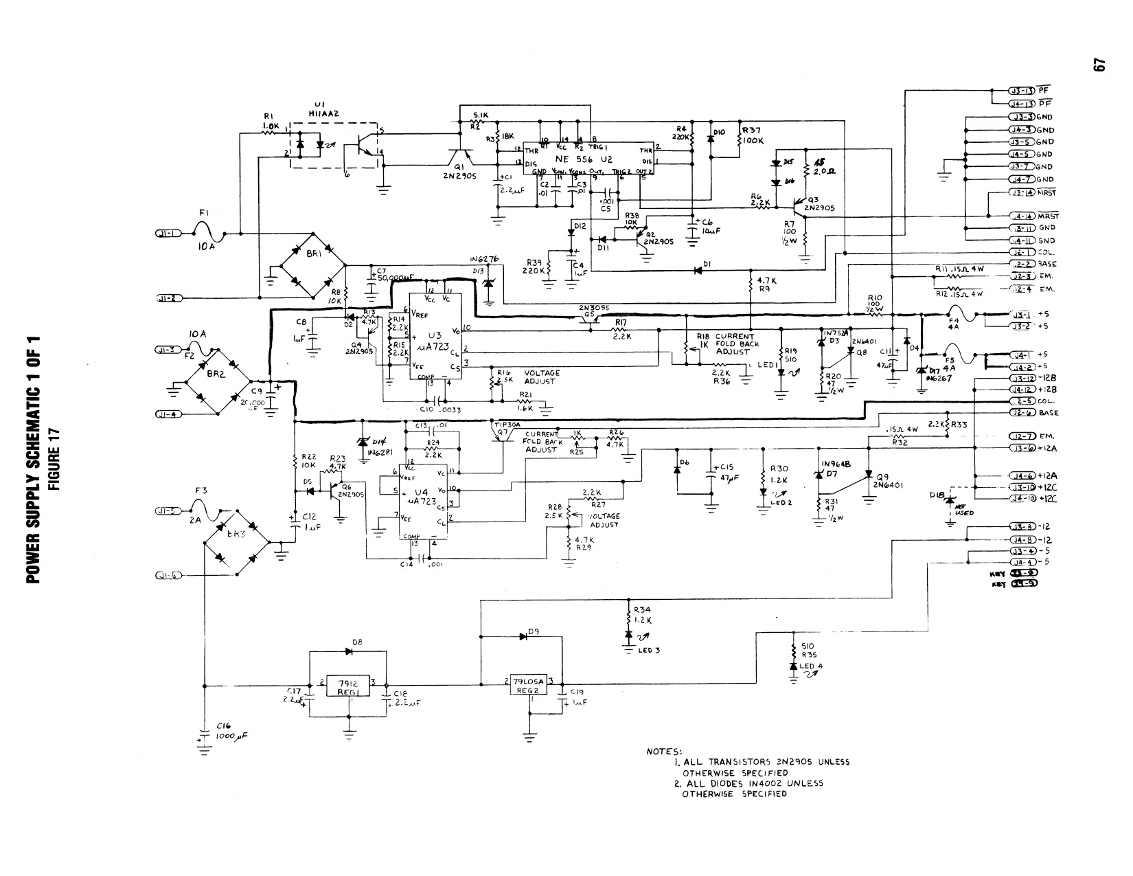
This page is a drawing, shown as the original scan.
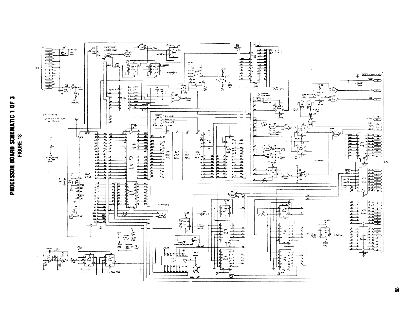
This page is a drawing, shown as the original scan.
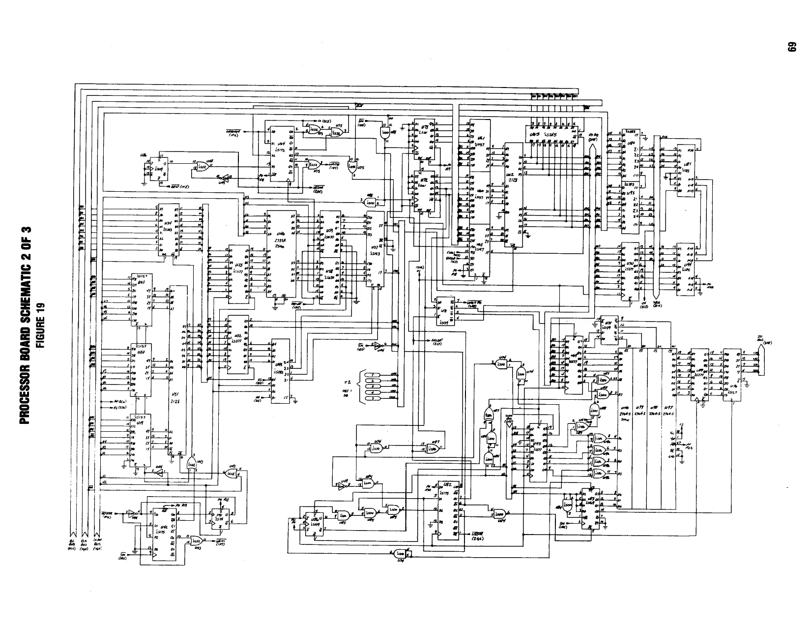
This page is a drawing, shown as the original scan.
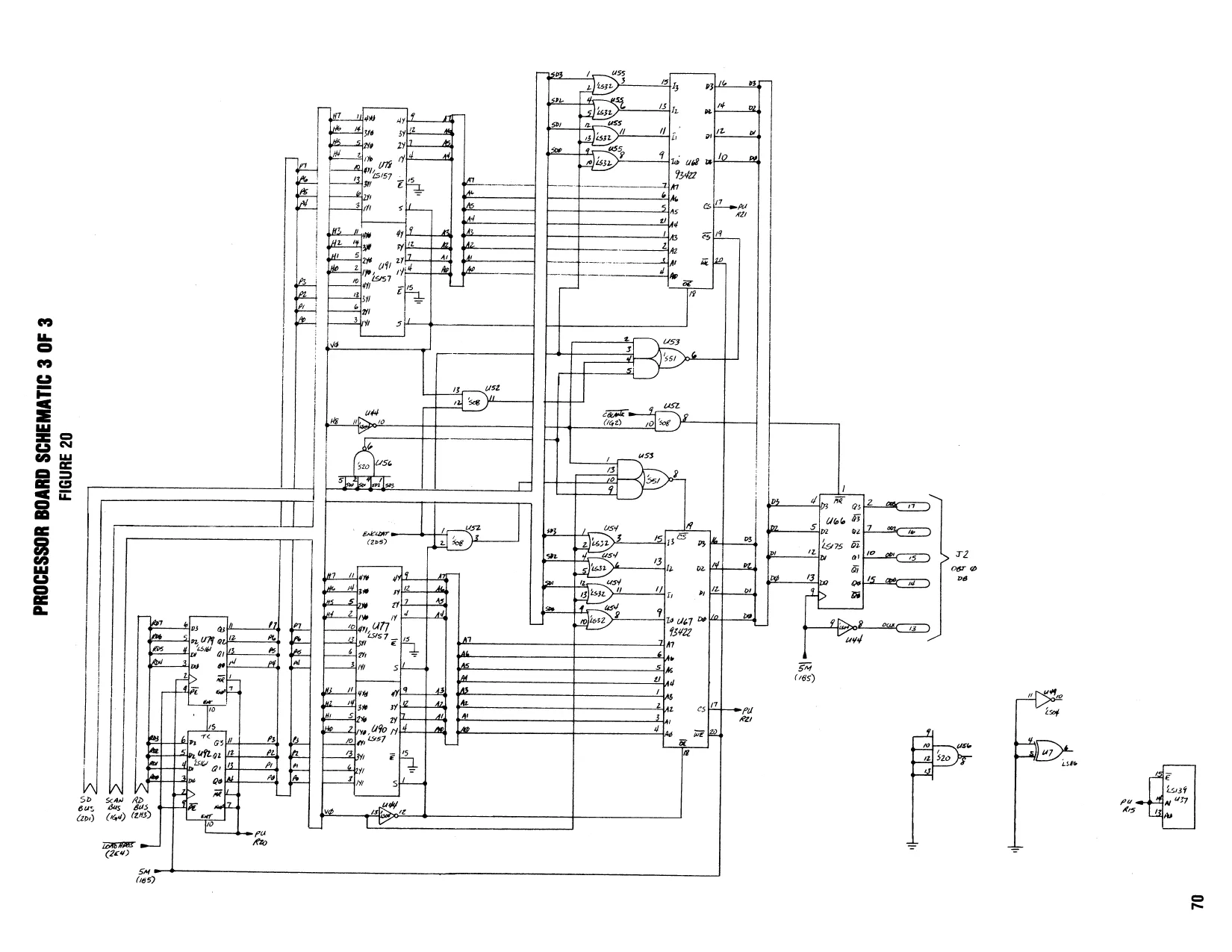
This page is a drawing, shown as the original scan.
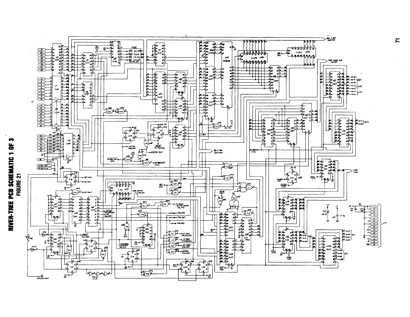
This page is a drawing, shown as the original scan.
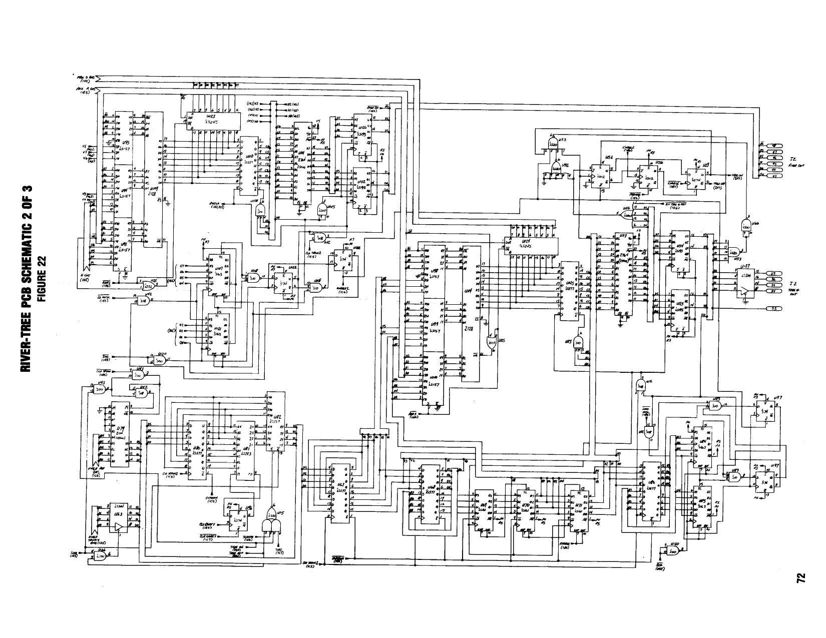
This page is a drawing, shown as the original scan.
€2 aHuNDId € 40 © SILWINSHOS 99d 33H1-Y3AI
vl
gt gate re
I aaara? see || Geta SHiEot
od v2 JUNI 2 40 L OILVINSHOS GUVOa 0/1 GNNOS
This page reads as a drawing: its text was drawn rather than typeset, and comes out in fragments. See the original scan.
[0 me Miter [ss oy ater
eigsle Magers Fiht |= no fam [#5 Sadey Soret Taian Bad ee ee ris [Ss see
a
ra
+
set ve: rey we
mre B | a vn locad
- earl ps7 fess ot 0007-004 ate 15-3 27}
| peeo ser | EE | cs fa | fis |
| 08-00/13 00! | worse be | et) ys yq [tee | rive |
‘arco [els sreanoatente theo ie ier mer ee
| A | sex} eye) | [eee | [pee 73% |
| rneec | | phere | Beit ggg g [BER | ley |
| wee [a peat | J | AE2l Rie | jv |
| {s| | = Ries ee | \| Gow |
Ffece _ eae meee ils
| jee | | | [eran aye-7 | [erro | [a] |
| goes | serail ayg.g | [mene | a ar |
fel rr pay y San eg [er 8 sy [ype she gg [r= 00 3 Jens.
| os [7p | ate yjoy | fox | |
| 13 tefeee | ee] vice [eee | tae | |
| evo [see | se yng | [ee | leme |
| i | r | caer Yr me | Pa |
cewo eee wee
| Po | ed 7 | r | ay ves |
eo J ae inn [eee mes, were Pee i we fe (efece eve li} FRTER AD. ve (eb a-c0res-o0T HB wer. 92 3uNdld