Red Baron DP-169-1st-03B
Red Baron (revised hardware) (Atari, 1980) · Drawing Package · 1 pages · original scan
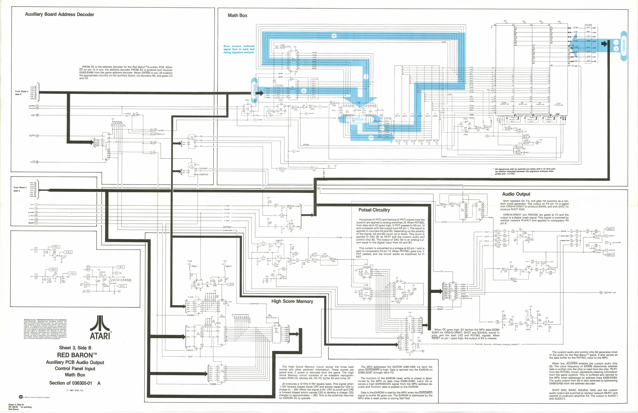
Auxiliary Board Address Decoder Math Box
= ;
signal flow of each test my 3
‘during signature analysis. i ch nie Bras baal PROM AS Is the address decoder for the Red Baron™Auxiliary PCB. When 5 “
EAB3-EAB6 from the game address decoder. When ERIWB is low, AS enables — Pe
ae
roma EE E ‘Side A a pe
ers fess [eset oun cer nA,
ORIGIN
er | son ae
Audio Output
Shift registers E4, F4, and gate H4 function as a random noise generator. The output on F4 pin 13 is gated with CRSH4CRSH7 to produce BANG, and with SHOT to produce SHOT SND.
CRSH4-CRSH7 and RNOISE are gated at F3 and the
‘output is digital crash signal. This signal is summed by
resistor network R14-A17 and applied to comparator K4 pin 6. Potsel Circuitry
Horizontal (H POT) and Vertical (V POT) inputs from the Joystick are applied to analog switches J5. When POTSEL from data latch E3 goes high, H POT passes to KS pin 12 ‘and compares withthe output from KS pin 1. The result applied to counters A3 and B3. Depending on the polarity Of the signal, A3 and 83 count up or down. This count is nme applied to DAC B4 as PO-P7 and the custom audio and Control chip 82. The output of DAC B4 is an analog current equal to the digital Input from A3 and 83,
This current is converted to a voltage at KS pin 1 and is sent to comparator KS pin 13. When POTSEL goes low, V 7 Foor aerente retiree eet i
——— A seer
- es High Score Memory E
= ATARI al | Sheet 3, Side B | | 7 RED BARON™ a nen OL goes high, E3 latches the MPU data (EDBO- EDB7) for CRSHO-CRSH7, SHOT and SQUEAL sound inpulg_and the stat LED and POTSEL, signals. When IESET on pin 1 goes high, the output of E3 is cleared
‘The custom audio and control chip 82 generates most of the audio for the Red Baron” game. It also serves as the data butfer for the POTSEL input to the MPU. Auxiliary PCB Audio Output pee: Control Panel Input The High Score Memory circuit stores the three best scores and other pertinent information. These scores are The MPU addresses the EAROM (ABO-ABS) via latch AO, when EAROMWR is high. Data is latched into the EAROM on When low, ACHPEN enables the custom audio chip 182. The clock frequency of ERAVB determines whether data is written into the chip or read from the chip. PO-P7, Math Box Saved ern it power is Yemoved jrom the game. The High EDBD-EDBY twough lich F tom the POTSEL chu epesnt stan nates ore Memory circuit consists of an erasable reprogram- pate SEARS. ‘able ROM C0, latches AQ, H0, FO, butler EO and timer<i0." The function of the EAROM (read, write or erase) is deter the MPU when addressed by address lines EABO-EABS. i mined by the MPU on data lings EDBO-EDBS. Latch HO ro. ‘The audio output from 82 is also selected by addressing Section of 036305-01 A JO produces a 12 KHz 0-15V square wave. This signal when Celves a high EAROMCON signal from the MPU address de- EABO-EABS from the address decoder.
© 101 Aa ne
Dette fat ring Red Bron +15V forward biases diode CR7 and allows capacitor C54 to ‘charge to ~28V. When the signal is OV, CRT is cutoff and CRE is forward-biased which causes C53 to develop a charge. C53. ‘charges to approximately ~ 28V. This is the potential required for EAROM 0 to operate. Coder and function data Is passed to the EAROM. Data in the EAROM is read by the MPU when the EAROMAD signal to butter E0 goes low. The EAROM ls addressed by the MPU after a reset pulse or during Self-Test. SHOT SND, BAND, SQUEAL SND, and the custom audio output are summed at resistor network RB-AT and Applied to push-pull amplifier Ké. The output is AUDIO | and AUDIO I