Williams Z-Unit CPU Theory and Maintanence Manual
Z-Unit (Williams Electronics Games, Inc.) · Manual · 150 pages · 66 sections · original scan
ZAUNIT™" TrleORY AND
MAINTENANCE MANUAL
including...
- System Theory . Bus Systems
- Programmable Logic Devices
- Drawing Set
NARC and Z-UN/Tare trademarks of WILLIAMS ELECTRONICS GAMES, INC.
Z-UNIT Theory and Maintenance Manual c-3
Table of Contents
CHAPTER 1. SYSTEM THEORY. ....00..0....cccccecccsseecsseesteeseeesteentesseesneennees 141 Board-Level Discussion... Board-Level Summary.
System PC Boards. ............eccceccecssssssseesseseeseeeeeeseseecseseecseseseaeseeeseseseeeseceeansceeaeeeees 1-2 CPU Board.. ROM Board..
Sound Board. Interface Board... Power Supply Boards..
System Data Flowchart (Illustration).
System Components.. Component Types
GSP MicroprocesSot...............cccsessesesesssssseceseeeeeseenceeseecensseseseseeneensinessntesneesneesaneees 1-6 DMA... escssetscsesntesessssesssneeesssnecessneessuieessnieeesnesiiesnmeesiessniessieesessssneecesen TS
Video RAM. Video Display.. Components of Video RAM.
Z-UNIT Theory and Maintenance Manual C-4
Functions RAS and CAS..0.....cccsssessssesssseessssseessseeessee Z-Unit Block Diagram (Illustration) .......c.0cccc Bit Map and Palette RAM: Simultaneous Addressing
Bit Map RAM vs. Palette RAM (lilustration) Video RAM Output Data... Video RAM Data Flowchart (illustration).
Serial Address Bus Operation (IllUStration)........cccscccsccsssssssssescsessessessesseesses 1-13
1-14 Entrances to Color RAM 1-14
DIA Converter... eesescssecseesssecssecseecsssessneesnsessee Color RAM to Monitor Drives (illustration). Picture Display Process Summary.
Image Data Flowchart (IMUStration)........cccccssccccssssssesssssstessessessessessessesseeseseeese 1-18
ROM. Image ROM.. Program ROM.. 1-19 1-19
Battery Backup. Memory Protection..
2-UNIT Theory and Maintenance Manual C-5
Reset/Watchdog Circuit Enables CMOS RAM.........cccsssssesssesseessessessressesseeseceens 1-20
12 Bus Systems. GSP Buses....... Map RAM Buses.
VO Ports Background and Interface Board Latches Diagnostic Display Port...
SOUN PoOrt.....sseseccsssssescsssssessesnsesseessnscsessssusecsssseesesssseesssssusssssaveccesuvecssssssessnuecensuseesaseees 1-26
Sound Board Common Feature: Theory of Operation...............
Sound System Data Flowchart (Illustration). Sound Computer (Simplified) //ustration
CHAPTER 2. BUS SYSTEMS ..00.0....000..ccccccccccccsscessssseesessnseeesesseessnsnensneees 2-1 The 12 Bus Systems. Four Bus Group................
2Z-UNIT Theory and Maintenance Manual C-6
Multiplexed Local Bus. Separate Local Buses.......
Z-Unit Block Diagram (Illustration)...
Video Address and Data Buses... Origin of the Video Address and Data Buses (Illustration).
Object Palette Bus. Serial Data Bus...... 2-7 Color Address and Data BUSeS........c:sccssssssssssssssssissnsnsttsnsssssitssissseeeeseen. 2-8
The Three Entrances to the Color Address Bus (Mustration).....0.0ccccc00. 2-9
ROM Board Buses... Source Address Bus.
Interface Board Data Bu: Background Data Bus
2Z-UNIT Theory and Maintenance Manual C-7
CHAPTER 3. PROGRAMMABLE LOGIC DEVICEG..................... 3-1 A Chip-Level Summary...
Statement of Intent How to Use This Chapter...
The Seven Devices.
Address Decoder Inputs to ZADDRDEC U80 (Table). OUPUTS..0.eeceeseecsseesseecseeeeseessee nC)
ZADDRDEC PLD U80 (IIUStratiON)........ccccccsceeeseesestessescssessessessessnstsssenssissessseeteeed 3-4
Autoerase Control... INPULS.... seers AUTOERASE PLD U20 (illustration)...
Outputs
Color RAM Control... Write Operations...... ZCRAMCTL PLD U28 (Illustration)...
Reading the Color RAM Inputs to ZCRAMCTL U28 (Table). Outputs from ZCRAMCTL U28 (Table)...
2Z-UNIT Theory and Maintenance Manual Cc-8
Image ROM Control ZIROMCTL PLD U83 (Illustration) Inputs.
Local Control... eeccccscssesssesssesssseessueessesssssesses Inputs to ZLOCLCTL U78 (Table). Outputs
ZLOCLCTL PLD U78 (IllUStration)......cccsssscsssssssssssssssssssssssssesessssssssseesssessesseseee 3-18
Video RAM Control...
Outputs.
ZVRAMCTL PLD U79 (Illustration). ......cccccsssssssssessssssetsssssssesssssssscssssssssveccssseeees 3-21
Video RAM Sequencer. Inputs to VRAMSEQ U12 (Table,
VRAMSEQ PLD U12 (Iilustration) Video RAM Sequencer Outputs............ Outputs from VRAMSEQ U12 (Table).
CHAPTER 4. GLOSSARY. “System Terminology............... *Complete Control Functions.
2-UNIT Theory and Maintenance Manual Cc-9
sElectronic and Logic Expressions.............0...cccccscccccsessssesssecsseesseesessseesseees 4-2
CMOS Circuit (MUStration).........esscscssssessssssseesssssesssssussecesstsesssssesssssesecsssescessiveceess 4-7 Video DAC (Illustration)... NAND Gate (I/lustration) XOR Gate (Illustration)...
CHAPTER 5. ELECTRONIC DRAWINGS. Interboard Wiring..........ccccccseeeeeees C-11879 CPU Board Assembly Drawing.
C-11879 CPU Board Logic Diagram (Board 1, Sheet 1 of 1 1) C-11879 CPU Board Logic Diagram (Board 1, Sheet 2 of 14). C-11879 CPU Board Logic Diagram (Board 1, Sheet 3 of 11)
C-11879 CPU Board Logic Diagram (Board 1, Sheet 4 of 14). C-11879 CPU Board Logic Diagram (Board 1, Sheet 5 of 14). C-11879 CPU Board Logic Diagram (Board 1, Sheet 6 of 11)...
C-11879 CPU Board Logic Diagram (Board 1, Sheet 7 of VW)... C-11879 CPU Board Logic Diagram (Board 1, Sheet 8 of 1 1). C-11879 CPU Board Logic Diagram (Board 1, Sheet 9 of V1).
C-11879 CPU Board Logic Diagram (Board 1, Sheet 10 of 1 1) C-11879 CPU Board Logic Diagram (Board 1, Sheet 11 of 11)
C-12260 ROM Board Assembly Drawing C-12260 ROM Board Logic Diagram (Board 2, Sheet 1 of 7) C-12260 ROM Board Logic Diagram (Board 2, Sheet 2 of 7)...
C-12260 ROM Board Logic Diagram (Board 2, Sheet 3 of 7)... C-12260 ROM Board Logic Diagram (Board 2, Sheet 4 of 7)...
Z-UNIT Theory and Maintenance Manual Cc-10
C-12260 ROM Board Logic Diagram (Board 2, Sheet 5 of 7).......cccceeee 5-22
C-12260 ROM Board Logic Diagram (Board 2, Sheet 6 of 7).. C-12260 ROM Board Logic Diagram (Board 2, Sheet 7 of 7).. C-12037 I/O Board (Board 3) Assembly Drawing... C-12037 I/O Board (Board 3) Logic Diagram... Power-Wiring Diagram
C-12401 Switching Power Supply Assembly Drawing... C-12350 Sound Board (Board 10) Assembly Drawing.. C-12350 Sound Board (Board 10) Logic Diagram
C-12259 Sound Power Supply Assembly Diagram C-12259 Sound Power Supply Schematic Diagram Cabinet Wiring Diagram..........csccccccssseessssessesssteseesssecssees
2-UNIT Theory and Maintenance Manual C-11
Notes
Z-UNIT Theory and Maintenance Manual
Chapter 1. System
Theory
Board-Level Discussion
Board-Level Summary System PC Boards
System Discussion
Summary System Components GSP _ Microprocessor DMA Video RAM
Color RAM D/A Converter ROM Scratchpad RAM CMOS RAM
12 Bus Systems PLDs V/O Ports Sound Board
ZUNIT Theory and Maintenance Manual 1-1
Board-Level Discussion
Board-Level Summary
The Z-UNIT video system consists of five printed circuitboards, a number of switches and a video monitor. The circuitboards contain most of the system’s electronics. Switches provide controlling inputs for gameplay. The video monitor displays game action on a high-resolution screen. The functions of the five boards follow...
System PC Boards
CPU BOARD The CPU Board incorporates an MPU (Microprocessor Unit), the system’s intelligence. The MPU controls the system according to the program (instruction list) . The Z-UNIT System employs a special MPU called a Graphic System Processor or GSP. The GSP's circuitry is optimized for video applications. For instance, the GSP produces blanking, vertical and horizontal sync for the monitor. The GSP also provides RAS and CAS signals to the Video RAM. Furthermore, the GSP can trace cursor (character) position on the screen. Previous Williams games achieved these capabilities with logic outside the microprocessor.
Other noteworthy CPU Board components include control circuitry, and video memory in RAM form. The Video RAM stores a bitmapped representation of each picture that the GSP orders displayed. A DMA (Direct Memory Access chip) loads image data into the Video RAM. Eight bits of Video RAM are object-oriented. The second eight bits are color oriented. The resulting sixteen bits are fed down a data bus to a latch. After the latch, one data bit is discarded. The remaining15 bits address the Color RAM. The Color
RAM outputs a parallel data stream. With latches and buffers, the system converts this parallel output data to analog signals. These signals drive the RGB inputs of a color, video monitor. Other output ports control self-test indicator LEDs and gameplay-selected sounds.
ROM BOARD The ROM Board provides ROM storage for the programs which control video system operation. This board also incorporates a data base that supplies game data such as video images. The ROM Board contains the game and diagnostic programs and permanent data used by programs. ROMs on the board are divided by their application. The board contains one million by 32 bits of Image ROM. Also present are 128K by 16 bits of program ROM. Both ROM types are accessible to the GSP on the Local Address and Data Buses.
The DMA's Source Address Bus and Image Data Bus also connect to the Image ROM. During DMA access to the Image ROM, tristate buffers lock out the GSP. However while the DMA accesses Image ROM, the GSP may still access Program ROM.
SOUND BOARD The Sound Board is a slave computer with its own clock and two 68BO9E microprocessors. This computer produces sound effects and music on command from the GSP. The sounds and music are stored as binary information in on-board ROM chips. The microprocessor loads this data into RAM and selectively feeds it to a DAC. The eight-bit DAC (Digital to Analog Converter) outputs a low level audio signal. This signal is amplified on-board. From the Sound Board, the signal is routed to a four-ohm speaker system.
INTERFACE BOARD The Interface Board includes input ports. These ports interface the video system to the coin switches and player control panel. Inputs allow the GSP to check the status of player-controlled switches.
POWER SUPPLY BOARDS A seven-amp, switching power supply produces a regulated DC output of positive 5VDC. Positive and negative 12 VDC for the sound system originate at a separate, unregulated supply. In addition, a 6.3-volt AC circuit powers general illumination lamps.
System Discussion
Summary
THE CPU BOARD derives power from a separate, switching power supply. According to the program stored in ROM, the GSP orders a DMA to load data. The DMA assembles the appropriate data in Video RAM. Meanwhile the GSP loads the Color RAM. Then the GSP sends Video RAM data over the Serial Data Bus. A latch circuit addresses the Color RAM with the Video RAM data. The Color RAM outputs color data for each pixel.
The system latches Color RAM data into a digital to analog converter (DAC). The result is three analog signals fluctuating between four volts and zero. These R, G and B signals arrive at the game’s monitor. After further amplification there, the three signals drive the CRT’s three color guns.
NOTICE This book discusses numerous chips and control functions. Except as noted, the chips are on the CPU Board. Also except as noted, the functions are active low signals.
System Components
COMPONENT TYPES The major components of the Z-UNIT Video System can be divided into 12 blocks. This chapter discusses the 12 from a theoretical perspective. Here is a list of component blocks with a brief description of function...
- GSP microprocessor manages control functions
+ DMA coordinates image communication functions
- Video RAM, including Map RAM and Palette RAM
- Color RAM that maps from Video RAM output to RGB colors
« D/A Converter to produce video from Color RAM output
+ ROM, including Program ROM and Image ROM
« Scratchpad RAM for GSP program computations
. CMOS RAM for Bookkeeping Totals, Game Adjustments
+ 12 Bus Systems to interface DMA and GSP systems
« PLDs handle sequencing, decoding, other logic functions
- 1/0 Ports for the Sound Computers and player panel
«Sound Board produces sound effects and music
GSP Microprocessor
The Z-UNIT video computer is based on a Texas Instruments 34010 microprocessor. This 16-bit microprocessor was designed for graphic purposes. Consequently it is known as a Graphic System Processor (GSP).
GSP U18 operates at 48 MHz derived from primary crystal clock U38. NAND gate U37 inverts the oscillator’s output. Then the inverted clock signal is applied to GSP pin 5 (INCLK).
Various secondary clock signals derive from the main 48 MHz clock on the CPU Board. These signals provide timing for system operations. One of the most important clock signals is the 16 MHz +DOT.CLK. This function gates the Video RAM Sequencer, Color RAM Data Latch and Video DAC.
DMA Image communication functions in the 2-UNIT System are coordinated by an application-specific DMA. The exact operation of this chip is proprietary. However in basic terms, it controls several buses for the GSP. The GSP turns over buses to the DMA for excellent reasons: First, the DMA can handle data transfers more efficiently than the GSP. (For instance, the DMA can use a 32-bit bus to transfer bit maps. The GSP would use a 16-bit bus.) Second, system architecture permits the GSP to process data while the DMA is transferring data. Third, the DMA can simultaneously read the source data and write it to a destination chip. The GSP can’t perform simultaneous reads and writes.
Buses employed by the DMA all carry image data between memory chips. The buses include...
- The Source Address Bus
- The Image Data Bus
. The Video Address Bus
- The Video Data Bus
Video RAM
VIDEO DISPLAY The WILLIAMS Z-UNIT system produces a 512-by-400 pixel (picture element) video display. The color display appears on a high-resolution, RGB color monitor. The monitor completes a frame every 16.67 milliseconds. That rate corresponds to a 60 Hz. vertical scan. Although this frame rate is true to the NTSC standard, the horizontal rate is not. The Z-UNIT system completes a horizontal scan in 40 microseconds. That corresponds to 25 kHz, considerably faster than the 15,734 Hz NTSC line rate. The system does not produce interlaced frames.
The Z-UNIT screen may simultaneously display 32,768 different colors. Under program control, the GSP selects these colors from ROM. For each displayed pixel, the system stores a 15-bit binary code in Color RAM. This pixel code represents one of the 32,768 colors.
COMPONENTS OF VIDEO RAM TWO TYPES. The Video RAM circuit contains two types of RAMs. The first is the Bit Map RAM. During gameplay, this contains a binary representation of the image that the system orders displayed. The second RAM type is the Palette RAM. Into the Palette RAM, the system loads a number corresponding to a color palette. This “palette” refers to a group of
colors useful in rendering the bit-mapped image. The colors are digitally stored at the Color RAM.
VIDEO RAM TO COLOR RAM. The Color RAM associates one color per pixel. But the Palette RAM is much lower in resolution. It contains only one color palette per image. Of course an image may contain thousands of pixels. Again, think of the Palette’s contribution as a color group. Each color group is suited to a particular image. For example, one color palette or group contains the colors for a tree. Another palette or group contains the colors for a building.
The Palette RAM can assemble 128 color palettes from the 32,768 colors stored in Color RAM. But each bit-mapped image receives only one palette. And each palette contains 256 colors determined by Bit Map RAM data. The Bit Map RAM specifies one of these colors for each pixel in the image. At the Color RAM, the system retrieves the exactcolor for each pixel.
VIDEO BUS OPERATION. Bit Map RAM and Palette Map RAM are on the Video Address Bus. Either the DMA or the microprocessor may scan these RAMs. While reading or writing image data, the DMA controls the Video Address and Data Buses. Meanwhile, tristated buffers lock the GSP out of the Video Buses. The DMA interrupts the microprocessor when the DMA's operations are complete. At that point, the microprocessor may again access the Video Buses.
However the GSP may also remain active during DMA activity. In fact, during DMA activity, the GSP can operate the Local Address and Data Buses. With these buses, the microprocessor can access the Scratchpad RAM or the Program ROM. But the DMA can never access Scratchpad RAM or Program ROM.
FUNCTIONS -RAS AND -CAS Functions -RAS and -CAS (Row Address-Select and Column Address-Select) originate at the GSP. The system uses these active-low functions to latch addresses into the Video RAMs. Other timing signals
Z-UNIT Block Diagram Multiplexed Local Bus (LAD) 34010 Graphic System Processor
CE ; Video’ Video Data Address Source Bus Bus Address Bus A
128K x 14 7 Palette RAM
64K x 32 Bit Map RAM Sound- Select Bus SI
Image Data Bus
Image Address J 1M x 32
Bus Image
FROM
bject Palette Bus |. ron 128K x 16 Program Program ROM)D2ta Bus
Color Address Program Address Bus i | MASS ASHAARAAN
Serial
Notes: @ indicates bus latches, buffers or transceivers. Control Bus not shown. Player Controls
Interface Board Data Bus Background/Road Generator oa, CMOS RAM RM OO ON WNQndM™m™™™™Mn
64K x 16 Scratchpad RAM (7, Separate Local Separate Adbress Bus Local Data Bus
derive from programmable logic devices (PLD's). An example of such signals is each RAM chip’s output enable (-O£) function. The PLD that produces the -OE signal is configured as a sequencer.
MEMORY CELL MATRIX. The Bit Map and Palette Map RAM each contain 64K useful address locations. These locations are configured as a matrix of memory cells. That is, each memory cell appears in a column of rows. The system addresses Video RAM locations with two groups of eight, parallel address bits. First, during the RAS address cycle, eight address bits select the desired cell’s row. Then, during the CAS address cycle, another eight address bits select the cell’s column. With both the row and column provided, the cell itself is identified.
BIT MAP AND PALETTE RAM: SIMULTANEOUS ADDRESSING The Palette RAM occupies the same address space as the Bit Map RAM. That is, whenever the system addresses the Bit Map RAM, the Palette RAM is also being addressed. The GSP chooses a single color palette (constant value) from the Program ROM. While the DMA loads the Bit Map RAM, the GSP
Bit Map RAM Palette RAM
The shaded area is a bit map. Each cell in a bit map The shaded area is a palette. It occupies the same location in the Palette RAM as the bit map does in Bit Map RAM. Every cell ina palette has the same value. has a value of 0 to 255 (decimal).
Z-UNIT Theory and Maintenance Manual |-7 0
simultaneously loads the Palette RAM. The GSP saves itself some time by feeding the palette number into the Palette Latch. This latch actually loads the Palette RAM.
The result is corresponding addresses containing a bit map and a palette for that map. Using the same addresses for simultaneous loading of two devices saves time and hardware. But what about addressing confusion? Actually, no confusion results. The reason is separation of tasks: The DMA only loads the Bit Map and the Palette Latch only loads the Palette.
LOADING THE VIDEO RAM. The DMA loads bit-mapped data onto the 32-bit Video Data Bus. Meanwhile, the GSP loads palette data onto the Object Palette Bus. (The Object Palette Bus is derived by latching the 16-bit, Separate Local Data Bus.) The Video Address Bus accesses Video RAM every 166 nanoseconds. The DMA addresses both bit and palette memories simultaneously. Then the DMA loads 32 bits of data into the Bit Map every 166 nanoseconds. (That six megahertz rate corresponds to one eight-bit pixel every 47 nanoseconds!) Simultaneously, every 166 nanoseconds, the Palette Latch loads 32 data bits into the Palette Map.
Despite its 16-bit width, the Palette Latch achieves the necessary 32-bit transfers. Duplicate data is the key to this process. As mentioned earlier, the Palette Latch creates the 16-bit Object Palette Bus. (The new bus is a latched reproduction of the Separate Local Data Bus.) At the Palette RAM, each Object Palette Bus bit is connected to two destinations. This parallel wiring produces two identical bits for every bit on the bus. Resulting data duplication in the Palette RAM doesn’t matter. Remember that each palette is composed of a repeating, 16-bit constant (duplicate data) anyway.
Object Palette Bus
Serial Data Bus Color . h Serial eas Address Video
Data Palette Color RAM
Bus RAM
VIDEO RAM OUTPUT DATA
Video RAM data flows onto the Serial Data Bus. The Serial Data Bus is named for its serial pixel flow. This bus actually carries parallel data.
There are eight Bit Map and eight Palette RAM chips. Together these Video RAMs output 64 bits. However the Serial Data Bus is only sixteen bits wide. Obviously, data multiplexing is necessary. In fact, the Video RAM chips’ output is time-division multiplexed.
MULTIPLEXING. Each type 4461 Video RAM chip has four serial input/output (S/O) pins. Each of these four writes to the Serial Data Bus at a different time. A four-megahertz clock synchronously enables one output pin on each chip of the Video RAM. Shift registers inside the chips load data onto their output pins. The result is 16 simultaneous data bits that define a pixel (picture element).
4461 Video RAM Chios
Palette 2. (o Ny, ‘y *) palgesseeees ene
MLL LLL LL LLL LLL LLL LLL LLL LLL LLL LLL Serial Address Bus
LOW AND HIGH BYTES. One set of eight Bit Map data bits becomes the low bus byte. The Palette RAM’s situation is very similar. That is, four Palette bytes must enter the bus. Again, only one byte can enter the Serial Data Bus at a time. Since the Bit Map produces the bottom bus byte, Palette data occupies the top byte.
The system achieves two-byte transfers from Video RAM to bus at 16 megahertz. The two bytes ride the Serial Data Bus to the Serial Data Bus Latch. The Serial Data Bus Latch is the last chip before the Color RAM.
DISCARDED PALETTE BIT. At the Color RAM, the high byte from the Serial Data Bus chooses a palette. However at the Serial Data Bus Latch, the system discards the most significant data bit. The most significant bit is a palette bit. As a result, the Palette RAM can only specify 128 of 256 possible color palettes. However the Color RAM only contains 32K locations, and couldn’t use the top bit anyway. The low byte isn’t affected at the latch. Consequently the Bit Map RAM can specify 256 colors per palette. The latch addresses the Color RAM with the remaining 15 bits.
Color RAM The Color RAM contains over 32,000 color codes. Each color code is expressed by a 16-bit, binary number. As we’ve observed, any code is addressable by 15 Video RAM bits (215=32,768). While 32,768 colors are addressable, in current games only 8,192 colors appear onscreen at once.
THE SERIAL DATA BUS LATCH applies 15 Video RAM bits to Color RAM address pins. Color RAM data then determines pixel color. That is, each Color RAM address specifies one color code. The system chooses one pixel color from 32,768 possibilities stored in Color RAM.
However no image includes more than 256 colors. For example a man and a car may be onscreen at once. The system renders the man from a palette of 256 colors. The car’s palette includes a different group of 256.
ENTRANCES TO COLOR RAM The Color Address Bus connects the Color RAM to three different buses. HYou can think of these three as the entrances to Color RAM. These entrances operate selectively. The system tristates (turns off) buffers to non-used entrances. We've discussed the Serial Data Bus as an entrance to the Color RAM. The GSP can also update the Color RAM. For instance, the GSP loads colors during beginning boot. To achieve loading, bus buffers connect GSP buses to Color RAM Address and Data Buses. During a game, the Background Video Board can also address the Color RAM. An address buffer connects the Background Data Bus and the Color Address Bus. (There is no connection between the Background Data Bus and the Color Data Bus.)
D/A Converter COLOR RAM DATA LATCH. The Color RAM outputs 16-bit color codes. Each code creates a different combination of brightness levels for the monitor. After they’re output from the Color RAM, the codes are latched.
Also at the Color RAM Data Latch, the system discards the most significant output bit, This action leaves five bits each of what will become red, green and blue signals. That is, the system renders each color in five bits of resolution.
DAC. A simple digital-to-analog converter assigns different voltages to each code. The DAC (Digital-to-Analog Converter) sends each data bit to a separate pullup resistor. Due to the resistors, high bits produce less voltage than low bits do. There is roughly a two-to-one relationship between adjacent bit voltages.
SYSTEM OUTPUT TO MONITOR. Resulting analog voltages are fed to the monitor’s red, blue and green (RGB) input transistors. Each voltage corresponds to one of the 32,768 possible color combinations. (The GSP also creates blanking, vertical and horizontal sync signals for the monitor.) After amplification, the R, G and B signals drive the cathode guns of the CRT. As the monitor traces a line, the system’s eraser circuit also goes into action. The Auto-Erase Latch writes zeros over the previous line in the bit map. Erasure prepares the bit map to record the next image for the screen. After a half frame is erased, the system begins to load a new map.
Meanwhile the beam sweeps across the monitor screen, reproducing each pixel from the bit map. In fact, pixel order is identical in the bit map and on the screen. Furthermore, each screen image is rendered from a color group specified in the Palette RAM. These colors are recovered from the Color RAM.
H, V AND BLANKING SIGNALS. The H and V (horizontal and vertical) outputs from the GSP are inverted and fed to the monitor. Composite sync is also produced by combining the H and V signals in an XOR gate. Furthermore, blanking signals arrive at the gun drive circuitry. These signals assure that gun drive is cut off during retrace. Horizontal and vertical retrace signals coincide with the monitor's hardware retrace period.
Z-UN/T Theory and Maintenance Manual 1-15
To produce the system’s blanking signals, several functions are gated. Circuitry inside the Color RAM Control PLD and subsequent flip-flop dividers produces blanking. These blanking signals are known as +BLANK.S and -BLANK.S.
CPU Board Monitor
Buffer (DAC)
16-bit Color Data Bus Ce Z Color RAM
+BLANK.S = |H=NWAUTMANDAO
PICTURE DISPLAY PROCESS SUMMARY Here’s a step-by-step summary of the picture-display process:
- The GSP chooses 32,768 colors for the current display.
- The GSP loads the 15-bit value for each color selection into a Color RAM location. Each color’s address determines which pixel code will cause that color to be displayed.
- The GSP loads a constant (palette) into the Palette Latch.
10.
11.
12. The GSP chooses an image from the Image ROM. The DMA loads an eight-bit map of this image into the Bit Map RAM.
While the DMA loads the Bit Map RAM, the Palette Latch simultaneously loads the Palette RAM. The Palette RAM contains simple data. This data is an eight-bit number that identifies a single color palette. The number occupies Palette RAM addresses corresponding to those just loaded into Bit Map RAM. (Each RAM stores eight bits.)
The GSP causes the Bit Map and Palette RAMs to output their data. The RAMs bit shift their data out onto the Serial Data Bus. Despite its name, the Serial Data Bus carries a parallel data stream. The top eight bits derive from the Palette RAM.
The Serial Bus Data Latch discards the most-significant data bit (surplus palette data).
The system selects a color for display at each pixel location on the screen. The game uses up to 8,192 colors at once. Selection is achieved by addressing. The system addresses the Color RAM with latched bit map and palette data.
The system loads selected Color RAM data into an output latch.
The system converts the digital data to analog signals for the monitor’s color guns.
After a line of pixels appear on the screen, the Autoerase Latch begins operation. The CRT guns write a line, then the latch erases the corresponding data from the Bit Map RAM.
Eventually the CRT guns complete the painting of half a frame. The DMA responds by reloading the top half of the Bit Map.
Image Data Flow Chart
Bit Map RAM Palette Palette RAM Latch
Color Data Bus Latch
High-Res CRT Display
ROM There are two types of ROM in the Z-UNIT system. These are Image ROM and Program ROM. Image ROM is accessible to the DMA or the GSP. Either (but never both) can read Image ROM over the Image Address and Data Buses. Program ROM is accessible only to the GSP. To read Program ROM, the GSP employs the Program Address and Data Buses.
IMAGE ROM Image ROM consists of a million by 32 memory bits. This memory block is composed of 64 chips located on the ROM Board. Image ROM is accessible over the Image Address and Data Buses. Either the GSP or the DMA may address Image ROM. Of course both may not access Image ROM simultaneously.
PROGRAM ROM The 512 kilobit by one byte Program ROM block also resides on the ROM Board. Program ROM includes eight chips. While the DMA is accessing Image ROM, the GSP can simultaneously access Program ROM. Separate bus systems and tristate bus buffers permit such simultaneous activity.
Scratchpad RAM
The GSP uses the Scratchpad RAM for temporary storage of data and calculations. The Scratchpad RAM resides on the Separate Local Address and Data Buses. The GSP can write 65,536 words each 16 bits long into the Scratchpad RAM. This large memory is composed of the four RAM chips U60 through U63. While the DMA is accessing Video RAM, the GSP can simultaneously access Scratchpad RAM. Separate bus systems and tristate bus buffers permit such simultaneous activity.
CMOS RAM
BATTERY BACKUP Standby battery power maintains audit information and game adjustments stored in the system’s CMOS RAM. This read-write memory at U65 contains 8,192 eight-bit memory locations. During gameplay, the system writes audit information to the bottom half of CMOS RAM. The system reads this information as part of the high score signature attract mode. Game adjustments are stored in the upper half of this RAM. During game operation these locations are only read.
MEMORY PROTECTION To provide memory protection, a “memory protect” switch remains closed while the coin door is shut. This switch prevents writing to the upper half (high memory bits) of the memory. More importantly, the switch prevents players and collection agents from making game adjustments.
With the coin door open, writing to the top half is possible. So while you’re altering game adjustments, keep the coin door open. Why? Because you’re writing to the top half of CMOS RAM.
RESET/WATCHDOG CIRCUIT ENABLES CMOS RAM The Reset/Watchdog Circuit produces two reset pulses, -CSO (Chip-Select Zero Not) and -RESET (Reset Not). The -CSO is an active-low function applied to CMOS RAM pin 20. The active-low -RESET function is a systemwide reset signal.
FUNCTION -CSO enables the CMOS RAM. Meanwhile, Reset/Watchdog function VO outputs the CMOS operating voltage. This voltage output also connects to the CMOS chip’s CE2 enable pin. This pin enables the chip whenever the pin receives a high pulse. If game or battery power falls too low, the CMOS chip is disabled.
SYSTEMWIDE RESET SIGNALS (-RESET) occur for either of two reasons:
+ The power supply voltage is subnormal (A power-up or power-down condition is sensed).
- The reset button has just been pressed.
During power fluctuations or testing, -RESET pulses assure that the GSP system is forced into a stable state. -RESET pulses also assure that timing elements are synchronized when normal operation begins. After a reset condition, a nominal GSP restarts the main program. The GSP will execute system diagnostics and then enter the game program. In a nutshell, after resetting, the GSP begins its program at the beginning.
A computer without a reset pulse would respond to power fluctuations in a haphazard manner. instead of jumping to the beginning of its program, it might try to begin anywhere. For example, it might immediately try to send color signals to its monitor. Without data first loaded into color or video RAM, the screen display would be random. Or worse, the monitor might be damaged.
WATCHDOG FUNCTION. The Reset/Watchdog is also a timer that poses a special “deadline” for the GSP. Unless the Reset/Watchdog is cleared before one second elapses, systemwide reset occurs. A nominal GSP clears the timer by writing specific data to a memory address. The command to clear the Reset/Watchdog is a component of the game program.
During normal game operation, the system clears the Reset/Watchdog before a GSP reset occurs. If the GSP fails to clear the Reset/Watchdog, the reset pulse occurs. This reset pulse returns the game to Game-Over Mode. The reasoning behind Reset/Watchdog operation is this: A GSP that doesn’t clear the Reset/Watchdog isn’t executing proper instruction sequences.
For instance, static electricity can cause incorrect execution of a GSP instruction. The usual result is that the game computer becomes mired in an instruction loop. Resetting the system is better than permitting it to remain in a loop. With a frozen display or unpredictable performance, a looping game can hardly be profitable!
The 12 Bus Systems
Since we devote Chapter 2 to Bus Systems, only a brief summary follows.
According to their purposes, the 12 bus systems fall into four groups. These are GSP Buses, Mapper RAM Buses, ROM Board Buses and Peripheral Buses.
GSP BUSES THE MULTIPLEXED LOCAL BUS. The GSP directly employs two bus systems. The first is the system from which most of the other buses originate. This is the 16-bit, Multiplexed Local Bus, a time-division multiplexed system. The Multiplexed Local Bus begins within the GSP itself. However the GSP is one of two bus masters for the Multiplexed Local Bus. While the Autoerase Latch is operating, the Autoerase PLD interrupts the GSP. Then the Autoerase Latch takes control of the bus. During the GSP interruption, bus phase functions -RAS and -CAS derive from the Autoerase PLD.
THE SEPARATE LOCAL BUSES. The second GSP bus system consists of the Separate Local Buses. This set of address and data buses separates from the Multiplexed Local Bus. One-way latches produce the eight-bit Separate Local Address Bus. (Additional Bits are added by PLDs, as we'll see in Chapter 3.) Meanwhile bus transceivers create the 16-bit Separate Local Data Bus.
MAP RAM BUSES THE VIDEO ADDRESS AND DATA BUSES split off the Multiplexed Local Bus. Splitting is achieved by the same means used to produce the Separate Local Buses. The system uses these buses to write image data from ROM into the Video RAMs.
THE OBJECT PALETTE BUS is another secondary bus that originates at the Separate Local Data Bus. The GSP loads a 16-bit constant into the Palette Latch. The latch feeds this constant to the Palette RAM over the Object Palette Bus. Meanwhile the DMA specifies the addresses that will record the constant.
THE SERIAL DATA BUS is serial in terms of video pixels, not data bits. This bus carries eight bits each from the Bit Map and Palette Map RAMs. The destination of these 16 bits is the Serial Data Bus Latch.
THE COLOR ADDRESS AND DATA BUSES connect to the Color RAM. Both derive from the Separate Local Buses. Latches on the Color Address Bus allow the GSP or Video RAMs to access Color RAM. (The Serial Bus Data Latch is one of these latches.) In games that have one, a Background Board may also address the Color RAM. The GSP loads the Color RAM through the Color Data Bus. The Color Data Bus also carries selected color data to the Video DAC.
ROM BOARD BUSES THE SOURCE ADDRESS BUS. The Source Address Bus originates at the DMA. It joins the Image Address Bus (a Local Address Bus descendant) at the Image ROM. Using this connection, the DMA can use the Source Address Bus to access Image ROMs.
THE IMAGE ADDRESS AND DATA BUSES. Either the GSP or the DMA can address Image ROM over the Image Address Bus. Image ROM data enters a new bus called the Image Data Bus. It carries image data to the GSP for
processing, or to the DMA. The GSP receives image data over the Separate Local Data Bus in 16-bit form. The DMA receives 32-bit image data.
THE PROGRAM ADDRESS AND PROGRAM DATA BUSES. These 16-bit buses split off from the Local Address and Data Buses. The GSP employs them to access Program ROM. Program ROM contains the GSP's main program.
PERIPHERAL BUSES THE SOUND-SELECT BUS is a product of the Multiplexed Local Bus. The GSP employs the Sound-Select Bus to specify game sounds and music.
THE INTERFACE BOARD DATA BUS receives inputs from player and operator switches. Switch positions appear as binary data at a latch. The GSP polls this latch from the Separate Local Data Bus.
THE BACKGROUND DATA BUS connects to a latch on the Color Address Bus. The latch allows the Background Data Bus to select pixel colors for screening. Current games don’t include a Background Board.
PLDs
THE USE OF PLD CHIPS. Programmable logic devices (PLDs) derive many of the control functions for the system. Like fused PROMs, these devices are programmed at the factory. However, PLDs and similar logic devices (PALs,EPLDs,PLAs) have a different application than PROMs do. PLDs can mimic TTL random logic. This makes PLDs ideal replacements for cumbersome combinational logic constructed with numerous generic TTL gates. In one PLD, a designer can access 900 or more gates.
REPLACING PLD CHIPS. When you need to replace a PLD, order it from your authorized Williams distributor. Part numbers are provided in the Programmed Chip Summary in your game’s service manual. Just as with
EPROMs, there can be no substitutes from other manufacturers. Of course, the chip’s manufacturer only sells blank PLDs. Blanks won’t work in your game.
In your game, PLDs serve as sequencers, latches and address decoders, among other uses. In fact, the Z-UNIT System uses seven PLDs. You'll find them all on the CPU Board. Chapter 3 includes a circuit-by-circuit description of PLD applications in your game. Here’s a brief list by PLD function...
. Address Decoder (ZADDRDEC, U80)
. Autoerase Control (AUTOERASE, U20)
- Color RAM Control (ZCRAMCTL, U28)
- image ROM Control (ZIROMCTL, U83)
. Local Control (ZLOCLCTL, U78)
. Video RAM Control (ZVRAMCTL, U79)
. Video RAM Sequencer (VRAMSEQ, U12)
1/0 Ports
BACKGROUND AND INTERFACE BOARD LATCHES Current production Z-UNIT games don’t include a Background Video Board. Your game’s I/O port connects to the Separate Local Data Bus through a transceiver. This circuit includes octal transceiver chips U7 and U8 on the Interface Board. The Interface Board Data Bus originates at the other side of the transceiver chips.
The Interface Board accepts inputs from player switches at its readable buffers U1 through U5. The Interface Board Data Bus scans these buffers for a change of state. Changes, transmitted to the Separate Local Data Bus, appear on GSP data pins.
DIAGNOSTIC DISPLAY PORT A CPU-Board I/O latch provides outputs for the diagnostic LED display. The seven-segment display resides on the CPU Board. The display connects to latch U53 through current-limiting resistor pack U54. Bits from the Separate Local Data Bus control the latch.
SOUND PORT As on pinball games, Z-UNIT sounds are activated by sound-select lines. To produce sounds, the GSP pulls different combinations of select lines low.
SOUND-SELECT BUS LATCH. The sound port consists of the 16-bit, Sound-Select Bus Latch and the sound select lines. The Sound-Select Bus Latch specifies the GSP's sound selections to the Sound Computer System. CPU Board chips U39 and U59 perform this function. These chips latch 16 data bits from the Multiplexed Local Bus. On the Sound Board side of the latch, incoming data bits order sound effects.
SOUND LINES. The sound board is a slave computer system. It uses 11 of the latched select lines. Actually only eight of the eleven can specify sound effects. With these eight, the GSP can order 256 sound effects from each sound microprocessor. As observed, there are some additional lines. Current games employ three of these for control signals: -NMI.M,STROBE.M and -RESET.
CONTROL SIGNALS. -NMI.M stands for Non-Maskable Interrupt, Master, Asserted low, -NMI.M causes the Master Sound Microprocessor to cease its current operation. The microprocessor must then jump to a service routine. This routine sends the sound call to the Slave (Sound-Effect) Microprocessor.
When high, STROBE.M latches bits meant for the Master (Music) Microprocessor’s data bus. When asserted low, the -RESET line causes the sound system to reboot its software.
For future games, two acknowledgement lines (ACK.M and ACK.S) are available. Also, the -NMI line can be tied to function -COMM.TB. This is a control signal for the talkback port. Incidentally, the game only employs the eight-bit talkback port during diagnostic routines. This port is accessible at connector 10J2.
Sound Board
COMMON FEATURES Typical WILLIAMS sound boards have certain common features. Your game’s Sound Board is composed of two or more repetitions of the same circuits. Let’s study one of those circuits. Imagine a very basic sound system. This basic sound board’s main blocks include...
A 68BO9E microprocessor for music and one for sounds
- Abus system for each microprocessor
An I/O Latch for each microprocessor
- RAM
+ FOM
« A digital-to-analog converter chip (DAC)
An audio power amplifier
- A crystal clock
. A passive power supply for the power amplifier
THEORY OF OPERATION SOUND-SELECT LINES. Eight sound-select (data) bits enter the Sound Computer through an 1/O latch. Two-microprocessor boards (as in the NARC system) require tvvo additional “strobe” inputs and a second latch. These components double the number of sound calls that the board can process. In fact, dual-microprocessor boards can process 512 different sound calls. The master microprocessor handles 256 music calls. The slave microprocessor responds to 256 sound-effect calls. Each microprocessor has its own strobe line and data bus latch.
STROBE LINES. On schematics, one strobe line is known as STROBE.M. The other is called -NMI.M. Both lines are connected to the Master (Music) Microprocessor. Strobes determine whether a sound call will be handled by Master or Slave Microprocessor. When high, STROBE.M latches bits meant for the Master (Music) Microprocessor’s data bus. When low, -NMI.M sends the sound call to the Slave (Sound-effect) Microprocessor.
SOUND DATA OPERATIONS. According to the sound program stored in ROM, the Sound Computer assembles appropriate sound data. The 68BO9E microprocessor locates this sound data in ROM and loads it into onboard RAM. Next, the Sound Computer may send this sound data over the data bus to the DAC. (This technique is called “recorded sound.‘) Or the Sound Computer may perform an operation on sound data from RAM. (This technique is called "algo sound. ") For example, data may be clocked out of RAM at various speeds,
producing various pitches. Music data receives special treatment. After the RAM, music data passes through an extra chip. This is the YM2151 Yamaha organ chip.
Sound-Select Lines
Strobe Line
Microprocessor
In any case, the resulting sound data appears at a DAC. This device converts binary data to a positive and negative 12-volt sine wave. Next, the system preamplifies the DAC output. Then analog filters create high and low components for the system’s two-way speakers. Power amplifiers boost the signal current of these audio components. The amplified audio arrives at the game’s_ speakers.
SPEECH DATA. The Sound Board treats speech data slightly differently than it treats sound effect data. From ROM to RAM, the sound reproduction process is the same. However for speech, the next step differs from our description above. Instead of sending data to the DAC, the microprocessor clocks data through a flip-flop. A serial data stream results. The Sound
Computer feeds this to a CVSD chip (Constantly Variable Slope Delta modulator). This chip is another form of DAC. Filters remove digital artifacts from the CVSD's output. Then an amplifier boosts the analog result for the speaker system.
Sound Computer (Simplified)
, Crystal 68BO9E Sound Microprocessor siock
a ———
27256 or 27512 7 Sound-Select Lines
+S Strobe Line
ns 27256 or 27512 Sound ROM
27256 or 27512 |
a 27256 or 27512 i Sound ROM |
32K x 16 ee) 2064 Sound |
=— y i £ a a ° =
Static RAM wWiWwG6 Www ggxgsssssssssJ SENN AA AMT ANNAN TH
Sound Sound Sound Address Bus Control pata Bus Bus
Chapter 2. Bus
Systems
The 12 Bus Systems
Four Bus Groups
GSP Buses MULTIPLEXED LOCAL BUS SEPARATE LOCAL BUSES
Map RAM Buses
VIDEO ADDRESS AND DATA BUSES OBJECT PALETTE BUS SERIAL DATA BUS COLORADDRESSANDDATABUSES
ROM Board Buses SOURCE ADDRESS BUS IMAGE ADDRESS AND DATA BUSES PROGRAMADDRESSANDDATABUSES
Peripheral Buses
SOUND-SELECT BUS INTERFACE BOARD DATA BUS BACKGROUND DATA BUS
The 12 Bus Systems
Four Bus Groups
As we observed in Chapter 1, your Z-UNIT game supports 12 major bus systems. According to their application in the system, these 12 can be assembled into four groups. The groups include the GSP Buses, Map RAM Buses, ROM Board Buses and Peripheral Buses.
GSP Buses
MULTIPLEXED LOCAL BUS The GSP's Local Address and Data bus is time-division multiplexed. That is, there is only one 16-bit bus. This bus serves alternately as address or data bus. This Multiplexed Local Bus is also the source of most other buses in the system.
LOCAL BUS CYCLES. We’ve accounted for two GSP address cycles. In fact the GSP produces three bus cycles. These three cycles appear throughout the Local Bus System...
. Column address
. Row address
. Data
First, the GSP produces an eight-bit, column-address cycle. Meanwhile
the GSP asserts its active-low Column Address Select (-CAS) function. Next the GSP produces an eight-bit, row-address cycle. During this second phase, the GSP asserts its active-low Row-Address Select (-RAS) function. The last bus cycle is the 16-bit data phase. While this cycle prevails, the GSP asserts its active-low Data-Enable (-DE/V) function.
AUTOERASE LATCH AS BUS MASTER. Besides the GSP, the Multiplexed Local Bus has another bus master. This device is the Autoerase Latch. Periodically, Autoerase PLD U20 transmits interrupt function -GSP.HLT.REQ to the GSP's -HOLD pin. This function temporarily halts the GSP. Then Autoerase Latch U21 takes over control of the Multiplexed Local Bus.
The Autoerase Latch erases the bit-mapped image by writing bits corresponding to a color. The latch receives color data from lines 510 and 511 of the Bit Map RAM. (These lines reside in a bit map area that never appears on the monitor.) Latch bits replace image bits at bit map locations. These locations will be read to the screen. As each line is written to the CRT, bit map erasure proceeds one line behind.
SEPARATE LOCAL BUSES The Multiplexed Local Bus flows through address latches and data transceivers. These isolate Separate Local Address and Data Buses. The Separate Local Address Bus begins at one-way latches U27 and U82. Meanwhile the Separate Local Data Bus originates at two-way transceivers U14 and U31.
The Separate Local Data Bus devotes 16 bits to data transactions. The Separate Local Address Bus transmits two groups of eight bits. The first eight address bits leave the GSP on the Column-Address Bus Cycle (-CAS). Eight more address bits leave the GSP during the Row-Address Bus Cycle (-RAS).
Z-UNIT Block Diagram Multiplexed
34010 Graphic System Processor Local Bus (LAD)
Image Data Bus
Image Address J 1M x 32 Bus Image ROM
bject Palette Bus | Cd oe
Program ROM}Data Bus
Color ISK x 16 Color
Background Address
(Data Bus Data Bus Program Address Bus RSQ AQ00nngny
Notes: @ indicates Background/Road bus latches, buffers Generator or transceivers. Player sontol Bus not Controls : 8K x 8 CMOSRAM_I-
64K x 16 Scratchpad RAM Interface Board Data Bus Ri SPQVI@ GAnnnnn Hi pynynpnyggsssssso
Separate Local Data Bus Separate Local Address Bus
RAS AND CAS CYCLES. The Video RAMs reside on the Video Address Bus. The system uses its RAS and CAS bus cycles to address these RAMs. Either the GSP or the DMA may access the Video RAMs. However most data transfers are handled by the DMA.
Other chips apply RAS and CAS as if the two were a single address cycle. An example of this situation is the Scratchpad RAM. The Scratchpad RAM is a four-chip memory with 65,536 memory cells. To address this memory, a 16-bit function is necessary (216 = 65,536). However the Separate Local Address Bus is only eight bits wide. But RAS and CAS each provide eight bits. When both cycles address the Scratchpad RAM, 16 bits are available.
DATA CYCLE. During the Data Cycle, the GSP reads and writes data to memory chips and I/O ports. For instance, it may update Color RAM contents by loading data from the Image ROM. Or the GSP may write a sound-select instruction to the Sound Port.
Map RAM Buses
VIDEO ADDRESS AND DATA BUSES THE VIDEO ADDRESS BUS is one byte (eight bits) wide. This bus derives from the Multiplexed Local Address Bus at CPU Board latch U58. The system employs the Video Address Bus in addressing the Bit Map RAM. This RAM stores binary representations of video images.
THE VIDEO DATA BUS is 32 bits wide. These 32 bits originate at the 16-bit, Multiplexed Local Data Bus. Where do the top 16 bits come from? They’re duplicates of the bottom 16 bits from the Multiplexed Local Data Bus. The system feeds the bottom bits into two 16-bit transceivers (U15/32 and U16/33). The transceivers output two identical sets of 16 bits. These two sets become the 32 bits of the Video Data Bus: The bottom 16 read or write to the bottom half of the bit map. The top 16 read or write to the top half.
A transceiver becomes active when its -VDEN (Video Data Enable) signal goes low. To access upper data locations, the GSP asserts function -VDEN.H and turns on transceiver U15/32. To access lower data locations, the GSP asserts -VDEN.L, enabling U16/33.
-VDEN.H (high-bit enable signal) 16-bit transceiver
Multiplexed Local Bus (16 bits) @ no B a
transceiver U16/33 -VDEN.L (low-bit enable signal)
The system employs the Video Data Bus in loading the Bit Map RAM. A powerful DMA usually performs this task. The DMA (U77) is specifically designed for rapid bus transactions. It can transfer bit map data more efficiently than the GSP can. Furthermore the GSP may remain active during video data transfers.
During DMA data access, the GSP tristates (shuts off) its Video Data Bus buffers. Because the GSP remains active, buffer shutdown prevents bus conflicts with the DMA. Meanwhile the GSP uses the Multiplexed Local and Separate Local Buses and processes data. However during DMA inactivity, the GSP can access Bit Map RAM data pins.
OBJECT PALETTE BUS The Object Palette Bus is a data bus two bytes (16 bits) wide. This bus derives directly from the Separate Local Data Bus. In fact the Palette Data Bus and the Separate Local Data Bus carry identical information. The Object Palette Bus derives from the Separate Local Data Bus at transceiver U10/29.
Using the Object Palette Bus, the GSP can read or write data to the Palette. Such two-way access is actually rare. Two-way access occurs only during diagnostics.
PALETTES ARE NUMBERED, The system employs the Video Address Bus in loading data into the Palette RAM. This RAM stores a color palette number for each mapped image in Bit Map RAM. (For instance, there’s one palette for faces, one for buildings and one for trees. The colors that comprise each palette reside in Color RAM.)
PALETTE LATCH. During a game, the GSP sends a palette number to Palette Latch U13/30. The DMA simultaneously addresses Bit Map and Palette RAMs. As the DMA writes the bit map, the latch repeatedly writes the palette number. The resulting bit map has separate numbers in each bit map cell. But the resulting palette has the same number in each cell.
SERIAL DATA BUS The Serial Data Bus is two bytes (16 bits) wide. The name, “Serial Data Bus” refers to the serial flow of pixels, not a serial flow of bits. The bottom byte is bit map data, while the top byte is palette data. The Serial Data Bus runs between the Video RAM and the Serial Data Bus Latch. (Incidentally this latch is composed of chips U57 and U67.)
SERIAL DATA BUS LATCH. At the Serial Data Bus Latch, the system discards the most significant palette bit. This discard leaves 128 color palettes per picture. (Each palette has 256 colors.) The bottom byte describes eight levels of gray per pixel.
The Serial Data Bus Latch applies remaining bits to Color RAM address pins. The latch also counteracts propagation delay in lines and chips of the Video RAM section. After latching, the Serial Data Bus becomes the Color Address Bus. (There is no Serial Address Bus.)
COLOR ADDRESS AND DATA BUSES COLOR ADDRESS BUS. When addressing the Color RAM, the GSP employs the 15-bit Color Address Bus. This bus originates from the Separate Local Address Bus. The Separate Local Address Bus passes through a buffer to produce the Color Address Bus. The one-way buffer is composed of buffer chip U66 and latch U56.
The latch is necessary because the GSP sends eight address bits each on two bus cycles. At the latch (U56), the system discards the most signficant address bit. With the remaining 15 bits, the resulting Color Address Bus can address 32,768 bits. (That is, addresses up to hexadecimal EFFF).
LATCHED BUS ENTRANCES. Besides the GSP entrance, there are two other entrances to the Color Address Bus. Partly to prevent bus conflicts with the GSP, these secondary bus entrances are latched. Another reason for a latch is to correct bus and chip propagation delays. And a third reason is that both secondary entrances connect to data-carrying buses. Unlike the address buses in this system, most data buses are two-way buses. The latches separate two-way data from one-way data used as addresses.
OTHER ENTRANCES TO THE COLOR ADDRESS BUS. We've already discussed the entrance through the Serial Data Bus Latch. This entrance permits Color RAM addressing with Serial Data Bus bits from the Video RAMs. Another secondary entrance to the Color Address Bus is available to the Background Data Bus. Not all Z-UNIT games have Background Boards. In those that do, the Background Data Bus must communicate with the Color RAM. A data latch provides this one-way communication path. Chips U5 and U25 link the Background Data Bus to the Color Address Bus.
Enable & Separate Local Clock Signals Address Bus
Buffer
15-bit Color Address Bus
WH Color RAM
Data Bus Buffer
Background Data Bus Buffer
THE COLOR DATA BUS is 16 bits wide. This bidirectional bus derives from the Separate Local Data Bus. A two-way buffer, transceiver U4/24 connects the two buses. The GSP employs the Color Data Bus to enter Image ROM data into Color RAM. Moreover, Color RAM data selected by the Video RAM exits to the Color Data Bus.
COLOR RAM OUTPUT DATA PATH. The Color Data Bus carries 16-bit Color RAM output data to a latch. (This latch consists of chips U3 and U23.) The latch discards the most significant bit, but passes remaining data to a DAC circuit. Latch output is a five-bit number each for red, green and blue monitor inputs. The DAC (Digital-to-Analog Converter) must translate the numbers into analog voltages. (The DAC consists of buffer chips U2 and U22,
and resistors R2 through R16.) The DAC outputs 32 voltage levels each of red, green and blue to the monitor.
ROM Board Buses
SOURCE ADDRESS BUS THE SOURCE ADDRESS BUS originates in the DMA. This bus is 24 bits wide. The DMA uses it to address the Image ROM. After buffering on the ROM Board, this bus joins the Image Address Bus. One-way buffer chips U19,U20, U21 and U22 connect the two buses. (These chips reside on the ROM Board.) In turn, the Image Address Bus connects to the Image ROM chips.
IMAGE ADDRESS AND DATA BUSES
THE IMAGE ADDRESS BUS on the ROM Board is 24 bits wide. Through a buffer, the lower 16 bits join the Separate Local Address Bus. (This buffer is composed of one-way, tristate chips U8, U9,U10 and U11. These chips reside on the ROM Board.) Because of the bus connection, either the GSP or the DMA can address Image ROM. While the DMA is addressing the Image ROM, the tristate buffer locks out the GSP. Likewise during GSP access, another buffer locks out the DMA.
The Image ROM contains one megabit by four bytes of information. The DMA's wider bus can address Image ROM more efficiently than the GSP's bus can But even with 24 bits, directly addressing every cell in Image ROM is impossible. To address all the cells, decoding is necessary. Address decoders driven by functions from the ROM Control PLD select a chip enable line. Then only one ROM chip with a given address is active. (U6, U7, U17 and U18 are the ROM-Board chips that decode Image ROM addresses.)
THE IMAGE DATA BUS derives from the DMA. Since the DMA is on the CPU Board, the Image Data Bus begins there. However this bus also connects
to the Image ROM on the ROM Board. The bus is 32 bits wide. A two-way buffer joins it to the Separate Local Data Bus. This buffer is composed of ROM-Board transceiver chips U13 through U16.
During DMA accesses, the Image Data Bus buffer isolates the GSP from the Image ROM. At other times, the GSP can access Image ROM. Of course the DMA has quite an edge in bus-access efficiency over the GSP. This edge is partly due to bus width. The Image Data Bus is twice as wide as the Separate Local Data Bus. The 32-bit bus can transfer data twice as fast as the 16-bit bus can. Also, DMA bus transfers require less steps than GSP bus transfers do.
PROGRAM ADDRESS AND DATA BUSES THE PROGRAM ADDRESS BUS resides on the ROM Board. This bus is 16 bits wide. However it derives from the eight-bit Separate Local Address Bus. The eight-bit, Separate Local Address Bus is fed into a buffer and a latch. (These are ROM Board buffer U3 and latch U4.) During the column-address bus cycle, the top eight bits enter the latch. Then during the row-address cycle, the bottom eight bits enter the buffer. As the system asserts function +RAS, clocking the latch, 16 bits emerge from the chips. The system employs the Program Address Bus when it accesses Program ROM.
+RAS (high-bit enable signal) 8-bit, ROM Board latch U42
Separate Local Address Bus (8 bits) y LLL LLL Program Address Bus (16 Bits) 8-bit, ROM Board buffer U3
However, directly addressing all the memory cells with 16 bits is not possible. Instead, addresses must be decoded. The system employs PLDs to derive control signals for ROM-Board address decoder U5. The Address Decoder PLD, U80 on the CPU Board, is the main chip in this group. Address decoder U5 produces four Program ROM Output Enable (-PROE) signals. These turn on one ROM chip at a time.
The GSP can access Program ROM while the DMA is transferring data from Image ROM. Of course the DMA and GSP can’t access the same chip at the same time. After the DMA completes its assigned task, the DMA interrupts the GSP. Then the GSP may access the Image ROM or direct the DMA to do it.
THE PROGRAM DATA BUS is another ROM Board bus. Actually it’s a buffered version of the Separate Local Data Bus. ROM Board Bus transceivers U1 and U2 link the two, 16-bit buses. The GSP uses the Program Data Bus to read data from the Program ROM. During DMA bus accesses to Image ROM, the GSP can simultaneously access Program ROM.
Peripheral Buses
SOUND-SELECT BUS The 16-bit Sound-Select Bus resides on the CPU and Sound Boards. The Sound-Select Bus receives information from the Sound-Select Bus Latch. This latch (U39 and U59) is on the CPU Board. The Multiplexed Local Bus lies at the input side of the latch. (The Sound Board also has its own address and data buses. However these buses are local to the Sound Computer System. Since these buses aren't part of the GSP system, we won’t discuss them.)
The GSP uses the latch to send sound-select input data to the Sound Computer. The Sound Computer System’s eight sound-select inputs reside on
the Sound-Select Bus. If any combination of input bits is pulled low by the latch, a sound results. Strobe lines direct the sound selection to the Sound-Effect Computer or the Music Computer. The main system must simultaneously assert the strobe and sound-select lines.
Sound-Select Bus Latch U39/U59 (CPU Board)
16\ fF Multiplexed icroprocessor Local Bus Microp (Master)
Sound-Effect Microprocessor (Slave)
Sound Board
INTERFACE BOARD DATA BUS The Interface Board Data Bus resides on the Interface Board. This bus is 16 bits wide. It feeds data to the Interface Board Transceiver. This transceiver (U7 and U8) is also on the Interface Board. The Separate Local Data Bus lies at the output side of the transceiver. (There is no Interface Board Address Bus.)
The transceiver chips are selected by OR gate U6 on the Interface Board. Functions -BG.SEL (Background Video Select) and -DEN (Data Enable) serve as inputs to this OR gate. -BG.SEL is an active-low function that originates at Address Decoder PLD U80. (U80 resides on the CPU Board.) Active-high
function +DDOUT.C3 clocks the data-transfer (A-B) pin of transceivers U7 and U8. +DDOUT.C3 is a CPU Board signal buffered by U17 and produced by the GSP.
The Interface Board Data Bus receives information from the Interface Data Buffer. Also on the Interface Board, this buffer is composed of chips U1 through U5. The Interface Data Buffer connects player panel and other external switches to the game computer. A switch closure pulls one buffer bit low. The system polls this bit for status. Then the GSP computes a response and performs appropriately.
Buffer chips are selected by address decoder U9 on the Interface Board. Local Address Bus bits 01 through 03 and functions -LAL and -BG.SEL control the decoder. -LAL (Local Address Latch) is an active-low function produced by the GSP. -BG.SEL is the same signal that appears at the input of the OR gate.
BACKGROUND DATA BUS The 16-bit Background Data Bus resides on the Background Video Board.
Chapter 8.
Programmable Logic
Devices
A Chip-Level Summary
Statement of Intent The Seven Devices
Address Decoder Autoerase Control Color RAM Control
Image ROM Control
Local Control Video RAM Control
Video RAM Sequencer
A Chip-Level Summary
Statement of Intent In Chapter 1 we mentioned the many PLD chips employed by your Z-UNIT game. This chapter describes these devices and their purposes in the system. We discuss the devices in alphabetical order by their names. On illustrations of the PLDs, inputs are shown in numerical order on the left. Outputs are on the right.
The exact programming of the PLDs is proprietary. For this reason, this manual does not reveal their internal circuitry or their Boolean formulas. Instead our purpose is to provide information about inputs, outputs and general chip functions. Furthermore most system control signals appear at the inputs or outputs of the PLDs. In fact, studying the PLDs provides an insight into the operation of the entire system.
HOW TO USE THIS CHAPTER This chapter is not light reading! Rather, it’s intended for reference purposes. For example, you might need to know what signals enter PLD chip U80. You can find that information here. In fact, here you'll find each PLD's inputs and outputs documented. Moreover, on succeeding pages, you can locate data on most Z-UNIT control signals. For troubleshooting, this bit-by-bit viewpoint is valuable. But we admit that our approach lacks something in the way of a plot. We suggest that you consult, rather than read this chapter.
The Seven Devices
SUMMARY There are seven programmable logic devices in the system. As observed in Chapter 1, these serve as sequencers, latches and address decoders, etc.
Most PLD tasks involve memory control for the GSP. Two PLDs are associated with the Video RAM and one with the Color RAM. The Image ROM has its own control PLD. The fifth PLD is employed as an address decoder. The sixth enables devices on the two Local Bus systems. The Autoerase Control PLD performs the most unusual task. Line by line, it erases the bit map.
Address Decoder (ZADDRDEC, U80)
INPUTS TO ZADDRDEC U80 Pin Latched +1AQ | From Latch U8; 19 | +1AQ from U82, pin 19 Latched -TR From Latch U8} 1 8 | -TR from U82, pin 18 From Latch U8117 | Latched
| From Latch U8 : : From Latch U81 Separate Local Address bit From Latch U81] 12 | Separate Local Address bit
Address-Decoder PLD U80 enables different chips at various addresses in the system’s memory map. Inputs to the Address Decoder PLD come from the Local Address Bus. Most of these inputs are first latched at U81. The Address Decoder PLD has 10 output pins.
OUTPUTS Here’s a rundown on the output functions. Skipped pins aren’t used...
. Pin 9: -DMA.SEL is a chip-select signal applied to Custom DMA U77. To operate the DMA, several other control functions are necessary.
. Pin 11: -CMOS.SEL is a chip-select signal applied to Reset/ Watchdog chip U55. In turn, the Reset/Watchdog selects CMOS RAM U65. The Reset/Watchdog’s CMOS enable signal pulls the RAM’s pin 20, CE1 pin low. The Reset/Watchdog also keeps track of CMOS
-DMA.SEL -CMOS.SEL -PSEL -CSEL -ISEL To PLD U79, pin 5 To PLD U78, pin 5 -BG.SEL To PLD U78, pin 4 To Jumper W13/W14 ZADDRDEC PLD U80 From U81, pin 19 (latched +!AQ) From U81, pin 18 (latched -TR) From U81, pin 17 (latched LA25) From U81, pin 16 (latched LA24) From U81, pin 15 (latched LA23) From U81, pin 14 & LA18 From U81, pin 13 & LA1 77 From U81, pin 12 & LA168
input power. With input voltage below 3.8VDC, the Reset/Watchdog grounds CE2. When CE2 is low, the CMOS chip is disabled. To operate the CMOS RAM, several other control functions are necessary.
. Pin 12: -PSEL is a chip-select signal applied to address decoder U5 on the ROM Board. This function helps to select Program ROM chip outputs. To operate the Program ROM section, several other control functions are necessary.
. Pin 13: -CSEL is a chip-select signal applied to the Color RAM Control PLD. This function helps to select the Color RAM. To operate the Color RAM section, several other control functions are necessary.
. Pin 14: -ISELis a chip-select signal applied to ROM-Control PLD U83. Descendants of this function appear at address decoders on the ROM Board. These descendants help to select Image ROM chip
outputs. To operate the Image ROM section, several other control functions are necessary.
. Pins 15 and19 are unnamed inputs to Video RAM Control PLD U80. Off U80, pin 19, jumper W13 allows connection to U860, pin 1. Alternately, jumper W14 selects connection to U80, pin 3. Pin 3 of U80 is also connected to function -RAS and buffer U85. Function -RAS may be produced by either the GSP or by Autoerase PLD U20. The originator depends on which chip is master of the Multiplexed Local Bus. (Either GSP U78 or Autoerase Latch U21 can be bus master.) Buffered at U85 pins 6 and 7, function -RAS becomes -VWR.T3 and -VWR.T2. Descendants of these functions drive write pins on the Video RAMs.
. Pins 16 and 18 are unnamed inputs to Local Control PLD U78. Pin 16 of the Address Decoder PLD joins the Local Control PLD at pin 5. Pin 18 of the Address Decoder PLD joins the Local Control PLD at pin 4.
. Pin 17: -BG.SEL is a chip-select signal applied to address decoder U9 on the Interface Board. This function helps to select the Background Video Board (not used in NARC games). To operate the Background Video Board, several other control functions are necessary.
Autoerase Control
(AUTOERASE, U20)
The Autoerase Control PLD clocks and enables Autoerase Latch U21. The Autoerase Latch deletes one row (line) of data from the Bit Map RAM. The latch performs its duty as the succeeding line is written to the CRT screen.
After a line of pixels appears on the screen, the Autoerase Latch begins operation. The latch is always one line behind the CRT guns. The guns write a line, then the latch erases the corresponding data from the Bit Map RAM. Clearing proceeds down the bit map, line by line. The Autoerase Latch resides on the Multiplexed Local Bus.
Of 512 possible lines, the system only displays bit map lines zero through 399. The remaining 112 lines may be used for temporary line or image storage. Typically lines 510 and 511 are used as line buffers. After the latch erases a line, the system might substitute one of these lines.
INPUTS The Autoerase Control PLD has 13 inputs and 12 outputs. First we'll examine the inputs. Here’s a summary of the input functions. Skipped pins aren’t used...
+LCLK1 -AERASE.EN Autoerase -GSP.HLT.REQ -VRAS.COX PLD U20 -LINT2 -GSP.HLT.ACK -CAS -BLANK -RAS LADOO -LAL U77, pins Q15& MI3 Notes: (1) Bits with an DISABLE LAD- prefix originate at the Multiplexed Local Bus. (2) Bits with an -EN suffix serve to enable chips. (3) -H or -L suffixes refer to high or low bus bits. (4) An -INT suffix refers to a microprocessor _interrupt signal. +LCLK1 From U77, pin G3 From U77, pin L14 -SND.INT -LINT1 From U77, pin El -EXT.INT To U77, pin N2 To U77, pin Ml4- To U77, pin M2 -DMA.BSY To U21, CK, pin 11 To U21, OE, pin 1
Pins 1 and 21: +LCLK1 is an active-high clock signal that originates at the GSP.
Pin 2: -AERASE.EN is an active-low signal from CPU-Board latch U8. Data bit four on the Separate Local Data Bus is latched to produce this function.
Pin 3: -VRAS.COX is an active-low signal from CPU-Board DIP resistor U84, pin 4. The forerunner of this signal is the bit map clock -RAS. -RAS (Row Address Select) is produced by the GSP. This -RAS signal is buffered at U85 and output at pin 15 as -VRAS.CO. After attenuation at the resistor pack, the signal receives the "X" suffix to become -VRAS.COX.
Pin 4: -GSP.HLT.ACK is a halt-acknowledgment function output by the GSP. This is an active-low signal. -GSP.HLT.ACK is the precursor of a function that causes DMA activity to halt.
Pin 17: -BLANK is the active-low, video blanking output produced by the GSP.
Pin 18: LADOO is the lowest bit on the Multiplexed Local Bus.
Pin 19: TEST is also connected to the test input pin on the DMA. This pin is normally pulled high by SIP 5, resistor 9. The factory uses this pin for bus and DMA tests.
Pin 21: Please see Pin 1.
Pin 22: +DMA.GO arrives at the Autoerase PLD from output pin G3 of DMA U77. This is an active-high function. +DMA.GO also operates as the output-enable function for latch U66. This chip links the Multiplexed Local Bus to the Source Address Bus. The link allows
direct GSP access to the Image ROM. During DMA access to the Image ROM, the system tristates U66, locking out the GSP.
Pin 23: HLT.ACK is output by the DMA at pin L14.
Pin 24: -SND.INT, the active-low sound-interrupt signal, originates at Sound Board flip-flop U28, pin 4. On the Sound Board, this same signal is called ACK.M (Acknowledgement, Main Sound Processor). The CPU Board interprets this function as a handshake from the Sound Board. -SND.INT (ACK.M) isn’t used on NARC games.
Pin 37: -LINT1is an active-low interrupt function produced by DMA U77. This function appears at DMA pin FI. After the DMA completes a bus transfer, it asserts this function, interrupting the GSP. The GSP's-LINT1interrupt line is located at U18, pin 6.
Pin 38: WORM.CK is a clock produced by DMA U77, pin El.
Pin 39: -EXT.INT is an active-low interrupt function produced by devices external to the CPU Board.
OUTPUTS OUTPUTS FROM AUTOERASE PLD U20 include control signals for many devices, including the Autoerase Latch. Among these signals are -RAS and -CAS, used for bit map addressing. Here’s a summary of the U20 outputs. Skipped pins aren't used...
Pin 6: -GSP.HLT.REQ, an active low function, is sent to the GSP's -HOLD line (U18, pin 8). During an autoerase operation, the Autoerase PLD asserts -GSP.HLT.REQ. Then the Autoerase Latch takes control of the Multiplexed Local Bus. The Autoerase Latch uses the Multiplexed Local Bus to write over the bit map.
Pin 7: -LINT2 is an active low, local interrupt function. When jumper W10 is present, this signal can interrupt the GSP. GSP U18 receives -LINT2 on its pin 7. Function -LINT2 isn’t used in NARC games.
Pin 8: -CAS, is the column-address select signal. Actually the PLD-created -CAS is a substitute signal. This -CAS replaces the GSP-produced -CAS when GSP activity halts. The Autoerase PLD halts the GSP with function -GSP.HLT.REQ. The PLD’s -CAS is buffered at U1 1 and subsequently becomes -LCAS (Local CAS). Thereafter -LCAS is applied to Scratchpad RAM chips U60 through U63. -CAS is also buffered at U85 to produce -VCAS.CO and -VCAS.Cl (Video RAM CAS). After attenuation at DIP resistor U84, the system uses these signals to address the Bit Map RAM. The attenuated signals are called -VCAS.COX and VCAS.ClI X. Chips U46, U47, U72 and U73 receive -VCAS.CIX. Meanwhile, chips U48, U49, U74 and U75 receive -VCAS.COX.
Pin 9: -RAS, is the row-address select signal. Actually the PLD-created -RAS is a substitute signal. This -RAS replaces the GSP-produced -RAS when GSP activity halts. The Autoerase PLD halts the GSP with function -GSP.HLT.REQ. The PLD’s -RAS is buffered at Ull and subsequently becomes -LRAS (Local CAS). Thereafter -LRAS is applied to Scratchpad RAM chips U60 through U63. -RAS is also buffered at U85 to produce -VRAS.CO and -VRAS.CI (Video RAM RAS). After attenuation at DIP resistor U84, the system use these signals to address the Bit Map RAM. The attenuated signals are called -VRAS.COX and VRAS.CI X. Chips U46, U47, U72 and U73 receive -VRAS.CIX. Meanwhile, chips U48, U49, U74 and U75 receive -VRAS.COX.
Pin 10: -LAL (Local Address Latch) is a substitute active-low, latch-enable function. The PLD’s -LAL replaces the GSP-produced -LAL during GSP interruption -LINT.2. Periodically the Autoerase PLD creates this interruption. -LAL enters pin 1 of Video RAM
Control PLD U79 and Local Control PLD U78. A pin 19 jumper at Address Decoder PLD U80 links -LAL to other chips. If your game uses jumper W13, only U80 output is added to -LAL. Jumper W14 mixes function -RAS with function -LAL.
Pin 13: DISABLE becomes an input function for PLD U80, the Address Decoder. DISABLE enters pin 8 of that chip.
Pin 14: VID.EN enters DMA U77 at input pin M14.
Pin 15: WR, a write-enable function, enters DMA U77 at input pin L3. Function WR also joins function -WR from GSP U18, pin 40.
Pin 16: RD, a read-enable function, enters DMA U77 at input pin M2. Function RD also joins function -TROE from GSP U18, pin 41.
Pin 25: -DMA.BSY is an active-low signal. After inversion at buffer U78, -DMA.BSY enables the tristate outputs of latch U58 and buffer U85. -DMA.BSY enters buffer U78 at pin 13 and exits at pin
- The system feeds the function to pin 1 of U58 and pin 1 of U85. Function -DMA.BSY also serves as a halt request to DMA U77. The PLD asserts this function while the Autoerase Latch controls the Multiplexed Local Bus. At this time, the latch is erasing the bit map. The DMA and Autoerase Latch must not simultaneously write data to Bit Map RAM. -DMA.BSY shuts the DMA off. Meanwhile -GSP.HLT.REQ keeps the GSP off the bus.
Pin 31: This pin provides the clock bit to Autoerase Latch U21. The clock bit enters U21 at pin 11.
Pin 36: This pin enables the output of Autoerase Latch U21. The enable bit enters U21 at pin 1.
Color RAM Control (ZCRAMCTL, U28)
The Color RAM Control PLD supervises read-write operations at the Color RAM. Although many devices can address Color RAM, only the GSP can write to Color RAM. During the game, the GSP constantly alters Color RAM content.
WRITE OPERATIONS Before the GSP writes to Color RAM, Color RAM read-write pins must be low. The GSP uses an indirect means to pull the pin low. The GSP transmits functions -LAL, -DEN, -TROE and -WR to the Color RAM Control PLD. (That is, ZCRAMCTL or CPU Board U28.) The Color RAM Control PLD gates these and function -CSEL from the Address Decoder PLD.
Then the Color RAM Control PLD outputs function -CRWR (Color RAM Write). This function pulls Color RAM write pins low.
Next the GSP must activate the Color RAM’s tristate data bus transceivers (U4 and U24). These join the Color Data Bus and the Separate Local Data Bus. These transceivers are the traffic cops of the color data realm. If the Color RAMs are outputting data, these transceivers prevent input data from the GSP.
The system asserts +DDOUT.C1(Data Direction Out) on the “A-B” transceiver pins. This function derives directly from the GSP. Then a function from the Color RAM Control PLD enables the transceiver chips. This function appears on schematics as -CDEN (Co/or Data Enable). Finally the GSP sends the data through the transceivers and over the Color Data Bus. The states of GSP bits DO through D15 are recorded in Color RAM locations.
Z-UNIT Theory and Maintenance Manual 3-1 |
+BG. DETO -| RIORITY mmm Bae -DET1 -CAEN -LAL ZCRAMCTL PLD U28 -~CDEN
-DEN -CRWR
-TROE +TR.WR “WR To U26, pin 2 -BG.EN To U26, pin 12
READING THE COLOR RAM What about reading Color RAM locations? The Color RAM Control PLD becomes involved in read operations. For a read operation, it asserts a “high” on the Color RAM R/W pin. The GSP, Serial Data Bus Latch and Background Data Bus may each address Color RAM. Of these three, only the GSP may read or write to Color RAM.
COLOR RAM ADDRESSING. The GSP offers address bus access by enabling the appropriate tristate bus latch or buffer. This tristate device normally separates the Color Address Bus from the reading chip.
To use a tristate address latch or buffer, the system must clock the chip. The chip’s clock input triggers with function +RAS or +DOT.CLK. +RAS derives from the GSP. +DOT.CLK is a clock signal divided off the system clock. One of three functions from the Color RAM Control PLD must also enable chip output. These functions appear on schematics as -CAEN,-BDEN and -SDEN. (The acronyms stand for Color Address Enable, Background Data Enable and Serial Data Enable. These functions enable buffer outputs. The buffers permit Color RAM addressing by the GSP, Background Board or Video RAM, respectively.)
COLOR RAM OUTPUT DATA. With Color RAM Addressing taken care of, let’s review the output data path. 16 bits of data leave the Color RAMs and flow down the Color Data Bus. Transceivers U4 and U24 disconnect the Separate Local Data Bus from the Color Data Bus. The system asserts +DOT.CLK, latching the data at chips U3 and U23. Then the signals encounter buffers U2 and U22 and associated resistors. Gated by system function +BLANK.S, the circuitry converts the binary signal to analog form. The monitor’s red, green and blue input transistors receive this signal.
INPUTS TO ZCRAMCTL U28 [Fin [input Function [From Oh [pm Notes
| 1 | +BG.DETO | NOR gate U9 | 8 | |For future use |
| 2 | -BG.PRIORITY | Latch U8 | 14 for future use | |
| 3 | +BG.DET1 | NOR gate U9 | 6 | |For future use |
a Les ignal J Dale br a c olsen En LL
| -WR | GSP U18 | Write signal |
| -BG.EN | Latch U8 | Background Enable (future) |
| -CSEL | PLD U80 | hip-select signal |
OUTPUTS FROM ZCRAMCTL_U28 Pin output To Chip Pin Function
CAEN Latch US6 & a GSP addresses CRAM at US6
| : | Buffer _U66 | : | i | i |
tan
gach CRAM
| AM | a | : | \ | |
| 15 | TR.WR | PLD U12 | 11@ | u12 is VRAMSEQ |
1 8|To U26, pin 2]D Flip-flop U26 2 19 Jo U26, pin 12]D Flip-flop U26 412}
Image ROM Control
(ZIROMCTL, U83)
The Image ROM Control PLD provides enable signals to the 64 Image ROM chips. These chips are connected to the Source Address Bus on the system’s ROM Board. They contain a data base of bit maps and palettes. Selecting a few maps and palettes, the system loads them into Video RAM.
-ISEL.TOL SA20 Z| ROMCTL -DMA.SEL PLD U83 ASEL.E +DDOUT.C2 *{SEL.TOH
| . | Note: Bits with an LA- | -IDEN.H | |
| LAOO | prefix originate at the | -IDEN.L | |
| -DEN | Separate Local Address | SEL.TIL | |
| -ISEL | Bus. Similarly, bits | -| | . |
-DMA.GO with an SA- prefix -ISEL.T1H originate at the Source | Address Bus.
3-14 Z-UNIT Theory and Maintenance Manual
INPUTS The Image ROM Control PLD has eight inputs and seven outputs. First, let's examine the input functions. Skipped pins aren’t used...
. Pins 1 and 2: SA21 and SA20 are address bits on the Source Address Bus. This 24-bit bus originates at DMA U77.
. Pin 3: -DMA.SEL, the DMA U77's chip-selection bit, derives from Address-Decoder PLD U80.U80 outputs the active-low function at pin 9.
. Pin 4: +DDOUT.C2 is a buffered GSP signal. Buffer U17 outputs functions +DDOUT.CO through +DDOUT.C3.
. Pin 6: LAO0 is an address bit on the Separate Local Address Bus.
. Pin 7: -DEN is the data enable signal from the GSP. This active-low function appears on GSP pin 37.
. Pin 8: -ISEL, the Image ROM chip-select function, derives from Address-Decoder PLD U80.U80 outputs the active-low function at pini4.
. Pin 9: -DMA.GO is an inverted form of a DMA output function. The active-high +DMA.GO appears at DMA U77, pin G3. This output enters buffer U78, pin 11. The inverted output function exits U76 at pin 10.
OUTPUTS Outputs from the Image ROM Control PLD are employed on the ROM Board. Bit by bit, let’s consider these functions now. Skipped pins aren’t used...
. Pin 12: -ISEL.TOL, the chip-select signal, is applied to ROM Board address decoder U17, pin 4. The "L" suffix refers to ROMs connected to the lower 16 Image Data Bus bits. This is an active-low signal.
Pin 13: -ISEL.E, originally a spare chip-select signal, becomes bit 20 on the Image Address Bus. The Image Address Bus resides on the ROM Board. On current-production games, this address bit isn’t used. (In fact, NARC games only employ addresses |A00 through 1A16. Each bit appears twice. Bits with an "L" suffix address the bottom half of Image ROM. "H" suffix bits address the top half.)
Pin 14: -ISEL.TOH is the chip-select signal. The system applies this signal to ROM Board address decoder U18 at pin 4. The "H" suffix refers to ROMs connected to the upper 16 Image Data Bus bits. -ISEL.TOH is an active-low signal.
Pin 15: -IDEN.H is an image data enable bit. The "H" suffix indicates communications over the 16 high bits of the Image Data Bus. On the ROM Board, function -IDEN.H enables octal bus transceivers U13 and U14. These transceivers handle communications between the image Data and Separate Local Data Buses. Transceivers are actually the origin of the Image Data Bus: The system enables these two transceivers and the Image Data Bus’s high bits come alive. When the system enables its other two bus transceivers, the low bits pulse with activity.
Pin 16: -IDEN.L is an image data enable bit. The "L" suffix indicates communications over the 16 low bits of the Image Data Bus. On the ROM Board, function -IDEN.L enables octal bus transceivers U15 and U16. These transceivers handle communications between the Image Data and Separate Local Data Buses. Transceivers are actually the origin of the Image Data Bus: The system enables these two transceivers and the Image Data Bus’s low bits come alive. When the system enables its other two bus transceivers, the high bits pulse with activity.
Pin 17: -ISEL.T1L is a chip-select signal. The system applies function -ISEL.T1H to ROM Board address decoder U6 at pin 4. The
"L" suffix refers to ROMs connected to the lower 16 Image Data Bus bits. -ISEL.T1L is an active-low signal.
. Pin 18: -ISEL.T1H is a chip-select signal. The system applies function -ISEL.T1H to ROM Board address decoder U7 at pin 4. The "H" suffix refers to ROMs connected to the upper 16 Image Data Bus bits. -ISEL.T1H is an active-low signal.
Local Control (ZLOCLCTL, U78)
INPUTS TO ZLOCLCTL U78 [From Chip Pix [wares
4 From PLD U80_ | ZADDRDEC U80 5 From PLD U80_ | ZADDREC U80 -TROE GSP U18
eparate ocal Address be +DMAGO MA U77_ G3] - i LA10 Latch U82 14 | Separate Local Address bit
The Local Control PLD (ZLOCLCTL, U78) manages devices on the two Local Bus Systems. The Local Control PLD has 10 inputs. These come from the GSP, Address Decoder PLD, Local Address Bus and coin door.
OUTPUTS All of this PLD's outputs are active-low signals. Here's a rundown on the seven Local Control PLD outputs. Skipped pins aren't used...
. Pin 12: -SOUND.SEL clocks CPU Board data latches U39 and U59. The latches join the Multiplexed Local Bus with the 16-bit Sound Data Bus. The GSP can select game sound effects through these latches. Usually latch activity requires a low, “output enable” bit as well as a clock bit. However U39 and U59 require no such function, because their “OE” pins are grounded.
. Pin 13: -PDEN is an enable signal applied to ROM Board octal transceiver chips U1 and U2. These chips connect the Separate Local Data Bus and the Program Data Bus. To operate, the transceivers also require data-direction signal +DDOUT.C1.
. Pin 14: -IWR (buffered by U7 1) is the Image ROM Write signal. The system feeds function -IRW to the ROM Board twice, as -IWR.L and -IWR.H. Whether these two signals are used in your game depends on ROM Board jumpers. There are two relevant jumper wire pairs, W5/W6 and W11/W12. Only one jumper in each pair can be used. Even-numbered jumpers W6 and W12 are used simultaneously. The same goes for odd-numbered jumpers W5 and W11.When W6 is employed, -WR.L becomes Image Address Bus bit IA14L. Likewise, when W12 is employed, -WR.H becomes Image Address Bus bit IA14H. Conversely, in games using W5 and W11, the Source Address Bus provides |A14L and |A1 4H.
“DENG 12_SOUND.SEL 13, -PDEN From PLD U86, pin 18 ZLOCLCTL PLD U78 From PLD U80, pin 16 To U11, pin 7 18 cMos.wA
17 -MISC.SEL From PLD U80, pin 1 Separate Local Address LA16 +DMAGO Separate Local Address LA1 0
Pin 16: -CMOS.WR provides the write signal that permits CMOS RAM data adjustments (Bookkeeping Totals, Game Adjustments). When you open the game’s coin door, -CMOS.WR drops low (active). It appears on U65 CMOS RAM pin 27. When you close the coin door, -CMOS.WR goes high so players can’t alter game adjustments.
Pin 17: -MISC.SEL clocks CPU Board data latches U8 and U53. U53 serves as an I/O port off the Separate Local Data Bus. The latch connects to the CPU Board’s seven-segment diagnostic LED display. U8 connects the Separate Local Data Bus to various PLDs through these functions...
Functions -SPK.1 and -SPK.2 connect to the Video RAM Sequencer, but aren’t currently used.
Function -OBJ.PAL.EN can enable the Object Palette Bus Latch through the RAM Control PLD.
Function -AERASE.EN can enable the Autoerase Latch through the Autoerase PLD.
Functions -BG.EN and -BG.PRIORITY enable the Background Video Board through the Color RAM Control PLD.
Function +FG.SCRL1 and +FG.SCRLO can enable foreground video scrolling through the Video RAM Sequencer PLD.
Pin 18: -LRWR is the read/write signal applied to Scratchpad RAM chips U60 through U63. -LRWR stands for Local RAM Write. When this function is low, the GSP can write to the Scratchpad (Local) RAM. When -LRWR is high, the GSP can read the Scratchpad RAM. To accept data, a Scratchpad RAM chip also requires a low, “output enable” pulse. This pulse must be applied to
each RAM chip’s OE pin. This signal (-LROE) also originates in the Local Control PLD.
Pin 19: -LROE is the output enable signal applied to Scratchpad RAM chips U60 through U63. -LROE stands for Local RAM Output Enable. To be useful, each RAM also requires a “write” (low) pulse on its R/W pin. This signal (-LRWR) also originates in the Local Control PLD.
Video RAM Control (ZVRAMCTL, U79)
INPUTS TO ZVRAMCTL U79
ow Address-Select signal
Separate Local Address bit
PLD U20 9 U20-Autoerase PLD
Latch U27 From PLD U80 ZADDRECU80
The Video RAM Control PLD provides six output-enable signals to the Video RAM circuit. The Video RAM Control PLD has nine input pins. These connect to the GSP, Address Decoder PLD, Separate Local Address Bus and latch U8. (Incidentally, the U8 latch’s input comes from the Local Control PL D.)
OUTPUTS Here’s a summary of Video RAM Control outputs. Skipped pins aren’t used...
. Pins 12 and 13: These pins connect to buffer U85. RAM Control PLD Pin 12 joins U85 at pins 8 and 9. The corresponding output functions at U85 are -VWR.T1 and -VWR.TO. RAM Control PI-D Pin 13 joins U85 at pins 6 and 7. The corresponding output functions at U85 are -VWR.T3 and -VWR.T2. Descendants of these functions activate the read/write pins of Video RAM chips.
. Pin 14: -ODEN is an enable signal applied to CPU Board octal transceiver chips U10 and U29. These chips connect the Object Palette Bus to the Local Data Bus. To operate, the transceivers also require data-direction signal +DDOUT.CO.
. Pin 15: -TROE.C1X is an enable signal applied to Bit Map RAM chips 46, U47, U72 and U73. To operate these chips, several
other control functions are necessary. Between the PLD and the Bit Map RAM, -TROE.C1X is buffered by U11.
: Pin 16: -TROE.COX is an enable signal applied to Bit Map RAM chips U48, U49, U74 and U75. To operate these chips, several other control functions are necessary. Between the PLD and the Bit Map RAM, -TROE.C1X is buffered by U11.
To U85, pins a &9 To U85, pins 6 & 7 -~ODEN To U1, pin 5 18 To uit, pin 4 -LAL & Jumper Wig -DEN —2 -RAS & Jumper W14 Separate Local Address LAOO.d From PLD U80, pin 15 ZVRAMCTL PLD U79
“TROE 47 VEN. ey 18 -DMA.BS -VDEN.H -OBJ.PAL.Eb 19 -LDEN
. Pin 17: -VDEN.L is an enable signal applied to CPU Board octal transceiver chips U16 and U33. These chips connect low, Video Data Bus bits to the Multiplexed Local Bus. To operate, the Otransceivers also require data-direction signal +DDOUT.CO.
. Pin 18: -VDEN.H is an enable signal applied to CPU Board octal transceiver chips U15 and U32. These chips connect high, Video Data Bus bits to the Multiplexed Local Bus. To operate, the transceivers also require data-direction signal +DDOUT.CO.
. Pin 19: -LDEN is an enable signal applied to CPU Board octal transceiver chips U14 and U31. These chips connect the Separate Local Data Bus to the Multiplexed Local Bus. To operate, the transceivers also require data-direction signal +DDOUT.C1.
Video RAM Sequencer
(ZVRAMSEQ, U12)
INPUTS TO VRAMSEQ U12 Pin | Input Function | From Chip Pin +FG.SCRL1 Latch U8 oreground-Scroll signal 1 -SPK.1 Latch U8 /C inside U12 (future use) Latch U8
INPUTS Input bits at the Video RAM Sequencer derive from the GSP: Between the GSP and the sequencer, U8 latches Local Data Bus bits 0 through 7. After latching, four of the bits are renamed -SPK.O, -SPK.1,+FG.SCRL.1 and +FG.SCRLO. These new functions appear at Video RAM Sequencer inputs. For Video RAM Sequencer pin numbers, refer to the VRAMSEQ table. Other input bits gated by the sequencer include...
The GSP blanking signal (-BLANK)
. +TR.WR (Transfer/Write) from the Color RAM Control (ZCRAMCTL) PLD
: +DOT.CLK, a 16 MHz clock derived from the primary clock by flip-flop dividers
CMOS.A12 CMOS.A11 +FG.SCRL1
-SPK.1 VRAMSEQ PLD U12 S0ET0 -SOE.TOX -SPK.O -SOE.T1X
+TR.WR Note: All resistor -SOE.T2X
values are ohms.
+DOT.CLK Active-low signals -SOE.T3X +FG.SCRLO have "2" pret. To U6, pin 12
-BLANK have a "-" prefix. +SCLK Active-high signal: A
-WATCH.DOG
VIDEO RAM SEQUENCER OUTPUTS When the Video RAMs output serial data, the GSP controls the operation. The Video RAM Sequencer PLD produces control bits for the GSP. Video RAM outputs are sequenced with serial output-enable and serial clock bits. Clock
bit +SCLK (serial clock) is an active high signal. Serial Output-Enable bits -SOE.TOX through -SOE.T3X are active-low functions. (Their "X" suffix indicates that they run through a series resistor.)
Two other outputs of the sequencer become high-order address bits for CMOS RAM U65. The sequencer’s active-low -WATCH.DOG output can interrupt Reset/Watchdog chip U55.
OUTPUTS FROM VRAMSEQ U12 PPin [Output Function | To Chip [Pim Nves CMOS.A12 CMOS RAMU65] 2 |+High-order address. bit 10 CMOS.A14 CMOS RAM U65 23 |-High-order address bit | SE RAMS | 2 eral © “Enable fo
Map RAMs U48/U74; lette Mao RAMs U44/U7
Serial’ Output Enable for
Map RAMs U46/U72; ette Map RAMs U42/U68 TST
Chapter 4. Glossary
System Terminology
Complete Control Functions
Electronic and Logic Expressions
Z-UNIT Theory and Maintenance Manual 41
ACK.M, ACK.S. For future games, two Sound Board acknowledgement lines (ACK.M and ACK.S) are available. With these the Sound Board microprocessors may acknowledge GSP commands. The Master (Music) microprocessor may assert ACK.M. ACK.S is for use by the Slave (Soundeffect) microprocessor.
Analog. A circuit where voltage levels mimic the quantity being measured. Within limits of their power supplies, analog circuit outputs vary in proportion to their inputs. For example, assume that sound volume is being measured. An analog circuit might raise its output voltage when the sound amplitude increases.
ASIC. Application-Specific Integrated Circuit. A special type of integrated circuit prepared by CAD/CAM means. The artwork for this IC has space reserved for custom circuitry. Application-specific masks are prepared at the CAD station. These permit CAM equipment to produce the custom circuit economically, even in relatively low volumes. The resulting circuit can be more reliable than a circuit produced with off-the-shelf parts. ASIC technology also often reduces the parts count on a PC board. Labor reduction at the board-stuffing stage permits ASICs to be cheaper than conventional circuitry.
AUTOERASE. The PLD that controls the Autoerase Latch. U12 on the CPU Board.
-AERASE.EN. Autoerase Enable, an active-low signal sent to the Autoerase Latch. This signal originates at CPU-Board latch U8. -AERASE.EN is a precursor to signals used to enable the Autoerase Latch.
Autoerase Latch. U21 on the CPU Board. This circuit overwrites a line in the Bit Map RAM. The system erases (or overwrites) a line after that line appears on the monitor.
-BDEN. Background Data Enable, an active-low function produced by Color RAM Control U28. This PLD resides on the CPU Board. U28 asserts -BDEN when the Background Board is addressing the Color RAM. -BDEN enables bus buffers on the Color Address Bus.
+BG.DETO, +BG.DET1. Background Video Detect 0 and 1. Inputs to Color RAM Control PLD U28. Reserved for use on future games.
-BG.EN. Background Video Enable. Inputs to Color RAM Control PLD U28. Reserved for use on future games.
-BG.PRIORITY. Background Video Priority. An active-low input to Color RAM Control PLD U28. This PLD resides on the CPU Board. -BG.PRIORITY is reserved for use on future games.
-BG.SEL. Background Select. This active-low, chip-select signal originates at Address Decoder PLD U80. This PLD resides on the CPU Board. The system applies -BG.SEL to address decoder U9 on the Interface Board. This function helps to select the Background Video Board.
Bit. Binary digit. The smallest piece of information a computer can process. A bit represents a single base-two number (one or zero). To the technician, one bit is one line on a chip or bus. In a properly-operating computer, this line will either measure zero or five volts. These are DC voltages. (This definition omits rise time and propagation delay. These concepts are beyond the scope of this book.)
Bit Map RAM. The Z-UN/TRAM that contains image data. Bit maps are permanently stored in Image ROM. Under instructions from the GSP, the DMA loads several bit maps into Bit Map RAM. The system can use the maps in RAM to create video. Or they can be processed by the GSP before video production.
Binary. The computer numbering system consisting of only two values, zero and one. This system is also known as base two.
+BLANK.S, -BLANK.S. Blanking functions output at flip-flop U6 on the CPU Board. These two signals are gated descendants of the video-blanking signal produced by GSP U18. +BLANK.S enables video output buffers U2 and U22, which serve as Video DACs.-BLANK.S pulls red, green and blue analog drive lines low, blanking the system’s video output.
-BLANK. Active-low signal that blanks that CRT. -BLANK originates at GSP U18, and is an input at Video RAM Sequencer PLD U12. GSP U18 and PLD U12 reside on the CPU Board. -BLANK is an input to Autoerase PLD U20 on the CPU Board.
Blanking. The video signal that blanks the electron guns during horizontal or vertical retrace.
Buffer. A power amplifier chip suitable for digital purposes: (1) This chip operates off TTL or other digital power supplies. (2) The chip isolates the control circuit from output devices. (3) The chip provides sufficient current to drive more output devices than the control circuit can. (4) Some buffers operate in one direction. Others are two-way devices, isolating control circuit inputs as well as outputs.
Bus. A group of lines, each carrying one bit of data, employed for the same purpose. Common computer buses are the address, data and control buses. These originate within the microprocessor chip.
Bus cycle. The period the system devotes to performing an address or data transaction. These transactions require the use of one or more bus systems. Multiplexed buses, such as the Multiplexed Local Bus, are used for either data or addressing. (Of course data and address functions must not occur simultaneous/y.) Multiplexing reduces the number of board traces. The GSP in your game produces three bus cycles: Data, Row Address and Column Address.
Bus Master. The circuit that controls a bus is its master. Only one master can operate the bus at a time. In a typical computer, most buses originate at the microprocessor. Usually only the microprocessor can control bus cycles and devices on the bus. A DMA is another type of chip that can assume control. In your game, the Autoerase Latch and the Palette Latch also may be bus masters.
Byte. Eight computer bits. A computer can use a byte to define one character, quantity, etc.
CAD/CAM. Computer-Aided Drafting/Computer-Aided Manufacturing.
CAE. Computer-Aided Engineering.
-CAEN. Color Address Enable, an active-low function produced by Color RAM Control U28. This PLD resides on the CPU Board. U28 asserts -CAEN when the GSP is addressing the Color RAM. -CAEN enables bus buffers on the Color Address Bus.
-CAS. Column-Address Select. The active-low GSP function that selects a column of addresses in dynamic RAM. When the GSP is interrupted during DMA operations, -CAS is provided by the Autoerase PLD.
-CAEN. Color Address Enable. An active-low function produced by Color RAM Control PLD U28. The system applies this function to latch U56 and buffer U66. The buffer and latch permit the GSP to address the Color RAM. All these chips appear on the CPU Board.
-CDEN. Color Data Enable, an active-low function produced by Color RAM Control U28. This PLD resides on the CPU Board. U28 asserts -CDEN when the GSP is transferring data with the Color RAM. -CDEN enables bus buffers on the Color Data Bus.
CE2. A chip-enable function.
Chip. An integrated circuit or IC. A chip is a tiny, bug-shaped package that contains numeous transistors and other circuitry. Digital chips containing 500,000 gates (transistors, MOSFETs, diodes, etc.) are not uncommon. On your schematics, chips are usually abbreviated with the prefix “U.”
CMOS.A11and CMOS.A12. CMOS-RAM address bits. These originate at Video RAM Sequencer PLD U12 on the CPU Board.
CMOS RAM. Complementary Metal Oxide Semiconductor, Read-Only Memory. A read-write memory created with totem-poll circuits made with MOS transistors. Totem-poll circuits employ two transistors in series. One of these is an N-channel device and the other’s a P-channel device. The gates of the two devices are connected together.
CMOS Circuit
Input output
-CMOS.SEL. CMOS Select, an active-low chip-select function applied to Reset/Watchdog chip U55. In turn, the Reset/Watchdog selects CMOS RAM U65. The signal originates at Address-Decoder PLD U80. The CMOS RAM, Reset/Watchdog and Address-Decoder PLD appear on the CPU Board.
-CMOS.WR. CMOS Write, an active-low function. Function -CMOS.WR is an output of Local Control PLD U78. This PLD resides on the CPU Board. Function -CMOS.WR provides the write signal that permits CMOS data adjustments (Bookkeeping Totals, Game Adjustments). When you open the game’s coin door, -CMOS.WR drops low (active). It appears at CMOS RAM U65 on the CPU Board. When you close the coin door, -CMOS.WR goes high so players can’t alter game adjustments.
COIN.DR. The memory-protect switch (a hardware switch) produces the COIN.DR function. The memory-protect switch opens (rises high) when someone opens the coin door. Function -COIN.DR is an input at Local Control PLD U78. This PLD resides on the CPU Board.
Color RAM (CRAM). The RAM in your game that stores binary data corresponding to pixel colors. The GSP regularly transfers 32,768 colors into the Color RAM. Any of these colors may be selected by the GSP, Video RAM or Background Board. Selected colors appear at a DAC, where they’re converted to analog form. Next the system presents analog color information to the monitor. The system employs this pixel-at-a-time means to build an entire video image.
Color RAM Control PLD (ZCRAMCTL8). U28 on the CPU Board. The PLD that originates control signals applied by the system to Color RAM chips.
Color RAM Data Latch. The one-way buffer that connects the Color RAM to the Video DAC.
Color Palette. In your game, the binary number that corresponds to a group of colors. This number is a byte long (eight bits).
-COMM.TB. The Sound Board -NMI line can be tied to function -COMM.TB. This is a control signal for the talkback port. The game employs its eight-bit sound talkback port during diagnostic routines. This port is accessible at connector 1 OJ2.
CPU. Central Processing Unit. The intelligence of any computer, including the Z-UNIT video computer. A CPU consists of three basic parts. These include an Arithmetic and Logic Unit (ALU), memory (buffers) and a Control Unit (CU).
CRAM. Abbreviation for Color RAM.
-CRWR. Color RAM Write. Color RAM Write, an active-low function produced by Color RAM Control U28. This PLD resides on the CPU Board. U28
asserts -CRWR when the GSP is writing data to the Color RAM. -CRWR prepares the Color RAMs to receive data from the GSP.
-CSEL. Chip Select, an active-low function from Address-Decoder PLD U80. -CSEL is an input to Color RAM Control PLD U28. Both PLDs reside on the CPU Board.
-CSO. Chip-Select Zero, an active-low chip-select function.
Crystal Clock. The squarewave oscillator circuit that synchronizes computer operations. The crystal is a piece of rock. Its mass distorts in a particular way when a voltage is applied. In the clock circuit, an oscillator applies an AC voltage to the crystal. The crystal’s distortion tends to stabilize the frequency of the input waveform.
-CSEL. CMOS RAM Select, an active-low function produced by the Address Decoder PLD. The Address Decoder PLD is CPU Board chip U80. The system applies -CSEL to the Color RAM Control PLD.
CVSD. Constantly-Variable Slope Delta modulator. This is a special type of digital-to-analog converter circuit. CVSD is a very economical means of signal encoding that only records a waveform’s rate of change. The CVSD chip converts data into changes in an analog waveform.
Cursor. The position marker on a computer screen. The operator moves the cursor with the keyboard, joystick, mouse or other pointing device. A cursor roughly corresponds to the hero character in a video game.
DAC. Digital-to-Analog Converter. A circuit that converts several digital bits into a single analog output signal. One means of D-to-A conversion is employed by video circuitry in your game. The circuit is partly discrete, so you can see how it functions.
The lowest bit is connected to a high-value resistor. The next-higher bit is connected to a resistor of roughly half this first value. The next bit receives half this second resistor’s value, and so on. The other ends of these resistors are joined together and to the base of the monitor’s preamplifier transistor. The system applies either five volts or zero to each resistor. The resulting current varies in proportion to how many resistors are hooked to five volts or ground at any moment. The input transistor, being current controlled, varies its output voltage and current proportionately.
VIDEO COMPUTE& RGBMONITOR
+5VD0C, +12VDC
Digital input
Monitor Color Input Transistor (1 of 3)
Filter
Analog Output
D/A Converter. See DAC.
-DEN. Data Enable function produced by GSP U18 on the CPU Board. This function serves as an input to CPU-Board chips including the Color RAM Control PLD U28 and ROM-Control PLD U83. These PLD chips demultiplex the enable bit to produce enable signals for numerous bus buffers.
Digital. A circuit that uses voltage levels to represent binary numbers. (Binary numbers are zero and one.) When a digital circuit measures a real-world quantity, the circuit produces equivalent numbers. Operations on these numbers control circuit devices. In your game, the values representing zero and one are zero and five volts, respectively. Digital circuits produce these voltages from a stable, five-volt supply. For example, transistor switches may cut off (0) or permit (1) the flow of current.
+DDOUT.CO (+DDOUT.C1, C2, C3). Data Direction Out, Chip Zero; an active-high function. The system applies the four +DDOUT signals to transceiver chips. +DDOUT determines which way the data is flowing through these two-way chips. A low permits data to flow into the chip. A high permits data to flow out of the chip. +DDOUT appears in concert with ODEN or similar output-enable signals.
+DDOUT.C2. Data Direction Out, a buffered GSP output. Buffer U17 outputs active-high functions +DDOUT.CO through +DDOUT.C3. Function +DDOUT.C2 is one of the inputs at ROM Control PLD U83. (All these chips reside on the CPU Board.)
-DEN. Data Enable, an active-low signal produced by GSP U18 on the CPU Board. Function -DEN is an input at Local Control PLD U78.
DIP. Dual-Inline Package. The common, bug-shaped package that houses many types of integrated circuits.
DISABLE. An output of Autoerase PLD U20 on the CPU Board. DISABLE becomes an input function for Address Decoder PLD U80 on the CPU Board.
Discrete. Constructed with individually packaged gates. A transistor is a discrete part. An integrated circuit (which contains numerous
transistors) is not. A resistor is a discrete part. A Single-Inline Package Resistor (which contains numerous resistors) is not.
DMA. Direct Memory Access circuit. This circuit can transfer data directly between memory devices on the data bus. Because it is a secondary bus master, the DMA must receive permission to use the bus from the microprocessor. Of course the microprocessor can perform data transfers too. But the microprocessor must transfer data through itself. Such transfers require more steps than direct transfers performed for the microprocessor by its DMA.
-DMA.BSY. DMA Busy is an active-low signal output from Autoerase PLD U20.U20 is on the CPU Board. After inversion at buffer U78, -DMA.BSY enables the tristate outputs of latch U58 and buffer U85. Function -DMA.BSY also serves as a halt request to DMA U77. The PLD asserts this function while the Autoerase Latch controls the Multiplexed Local Bus. At this time, the latch is erasing the bit map. The DMA and Autoerase Latch must not simultaneously write data to Bit Map RAM. -DMA.BSY shuts the DMA off. Meanwhile -GSP.HLT.REQ keeps the GSP off the bus. -DMA.BSY is also an input to Video RAM Control PLD U79 on the CPU Board.
-DMA.GO. This function is an input at ROM Control PLD U83. This PLD resides on the CPU Board. -DMA.GO is an inverted form of DMA output function +DMA.GO.
-DMA.SEL. DMA-Select, an active-low signal that enables DMA U77 on the CPU Board. This function is an input to ROM Control PLD U83. -DMA.SEL is also an output of Address-Decoder PLD U80. The PLDs reside on the CPU Board.
+DOT.CLK. A 16 MHz clock function. +DOT.CLK derives from the primary clock at flip-flop U36 and NAND gate U37. The primary clock is a 48 MHz oscillator. Both clocks reside on the CPU Board.
DRAM. Dynamic, Random-Access Memory. A read-write information-storage chip whose data must be refreshed at regular intervals. Your game’s Bit Map RAM and Palette RAM are DRAMs. In these applications, refreshment is no problem. Since the game displays moving images, the system constantly feeds new information to these RAMs.
EPLD. Erasable, Programmable Logic Device. See PLD.
-EXT.INT. External Interrupt, an input to Autoerase PLD U20. Devices external to the CPU Board produce this function.
+FG.SCRL1, +FG.SCRLO. Foreground Scroll, active-high signals that indirectly control video. These functions originate at latch U8, and are inputs to Video RAM Sequencer PLD U12. This PLD resides on the CPU Board.
Game-Over Mode. The game enters Game-Over Mode after initialization or the assertion of -RESET (warm start). In this mode, the game displays its attraction message, requesting deposit of coins.
GSP. Graphic System Processor. The Tl 34010 microprocessor, which is designed for image processing. This microprocessor is the brains of the Z-UNIT video system.
-GSP.HLT.ACK. GSP-Halt Acknowledgment, an input to Autoerase PLD U20 on the CPU Board. The GSP outputs this active-low signal. -GSP.HLT.ACK is the precursor of a function that causes DMA activity to halt.
-GSP.HLT.REQ. GSP Halt Request, an active-low function, appears at the output of Autoerase PLD U20.U20 is on the CPU Board. During Autoerase Latch activity, the Autoerase PLD asserts -GSP.HLT.REQ. The
system sends the signal to the GSP's -HOLD line (CPU Board U18, pin 8). Please see -GSP.HLT.REQ.
-HOLD. When asserted low, this GSP input function causes the GSP to stop and wait. During an autoerase operation, Autoerase PLD U20 asserts this function. Then the Autoerase Latch takes control of the Multiplexed Local Bus. The Autoerase Latch employs the Multiplexed Local Bus to write over the bit map. The systemwide name for the -HOLD function is -GSP.HLT.REQ. Please see -GSP.HLT.REQ
High Bits. Binary information that appears on the higher-numbered lines of a computer bus.
Horizontal Sync. One of two video signals that keeps a pixel in step with game transmissions. Horizontal sync coordinates the beam as it traces from side to side across the CRT. In the Z-UNIT system, this signal is a 25 kHz, rectangular waveform.
Hz. Hertz, after Heinrich Hertz, the 1888 discoverer of radio waves. The term used to describe wave frequency in terms of cycles per second (Hertz).
+IAQ. Instruction Acquisition Cycle, an active-high function. When this signal appears (during -RAS), the GSP or other bus master may read data.
-IDEN.H. Image Data Enable, High bits. ROM Control PLD U83 outputs this active-low enable signal. -IDEN.H is an image data enable bit. The "H" suffix indicates communications over the 16 high bits of the Image Data Bus. On the ROM Board, this function enables octal bus transceivers U13 and U14. These transceivers handle communications between the Image Data and Separate Local Data Buses. Transceivers are actually the origin of the Image Data Bus: The system enables these two transceivers and the Image
Data Bus’s high bits come alive. PLD U83 resides on the CPU Board. Transceivers U13 and U14 reside on the ROM Board.
-IDEN.L. Image Data Enable, Low bits. ROM Control PLD U83 outputs this active-low enable signal. -IDEN.L is an image data enable bit. The "L" suffix indicates communications over the 16 low bits of the Image Data Bus. On the ROM Board, this function enables octal bus transceivers U15 and U16. These transceivers handle communications between the Image Data and Separate Local Data Buses. Transceivers are actually the origin of the Image Data Bus: The system enables these two transceivers and the Image Data Bus’s low bits come alive. PLD U83 resides on the CPU Board. Transceivers U15 and U16 reside on the ROM Board.
Image ROM. The Read-Only Memory that permanently stores bit maps for your Z-UNIT game.
INCLK. Clock Input to GSP U18 on the CPU Board. The main system clock enters the GSP here.
VO. Input/Output. One of the four sections of computers with von Neumann architecture, such as your game. The four sections include the RAM, ROM, I/O and microprocessor. The I/O Section interfaces communication devices, such as a joystick and monitor, to the computer. Other computers, such as your game’s Sound Board, may also be connected to \/O ports.
IRQ.M,IRQ.S. Interrupt Request-Master and Interrupt Request-Slave. These microprocessor-interruption functions appear on Sound Board logic diagrams. The “master” and “slave” terminology refers to the Master Microprocessor and Slave Microprocessor. Each 68BO8E microprocessor has an Interrupt-Request input pin. Function STROBE.M triggers flip-flop U26 to produce -IRQ.M and output 6. Similarly, -COMM.M triggers flip-flop U26 to
produce -IRQ.S at output 8. In NARC games, -COMM.M is disconnected. However STROBE.M and IRQ.M produce a sound call to the Master Microprocessor. For more information, please see STROBE.M.
-ISEL. Image ROM Select, an active-low function produced by the Address Decoder PLD. The Address Decoder PLD resides at CPU Board location U80. The system applies -ISEL to ROM-Control PLD U83.
-ISEL.E. Image ROM Select, Extra. Originally a spare chip-select signal, -ISEL.becomes bit 20 on the Image Address Bus. On current-production games, this address bit isn’t used. -ISEL.E is an output of ROM Control PLD U83 on the CPU Board.
-ISEL.T1H. Image ROM Select 1, High bits. ROM Control PLD U83 outputs this active-low, chip-select signal. This PLD resides on the CPU Board. The system applies -ISEL.T1H to ROM Board address decoder U7. The "H" suffix refers to ROMs connected to the upper 16 Image Data Bus bits.
-ISEL.T1L. Image ROM Select 1, Low bits. ROM Control PLD U83 outputs this active-low, chip-select signal. This PLD resides on the CPU Board. The system applies -ISEL.T1L to ROM Board address decoder U6. The "L" suffix refers to ROMs connected to the lower 16 Image Data Bus bits.
-ISEL.TOH. Image ROM Select Zero, High bits. This active-low, chip-select signal is an output of ROM Control PLD U83. The "H" suffix refers to ROMs connected to the upper 16 Image Data Bus bits. The system applies -ISEL.TOL to ROM-Board address decoder U18 at pin 4. The decoder selects Image ROM chips. PLD U83 resides on the CPU Board. Decoder U18 and the Image ROMs reside on the ROM Board.
-ISEL.TOL. Image ROM Select Zero, Low bits. This active-low, chip-select signal is an output of ROM Control PLD U83. The "L" suffix
refers to ROMs connected to the lower 16 Image Data Bus bits. The system applies -ISEL.TOL to ROM-Board address decoder U17 at pin 4. The decoder selects Image ROM chips. ROM Control PLD U83 appears on the CPU Board. Decoder U17 and the Image ROMs reside on the ROM Board.
LA-. Local Address. This abbreviation will always be followed by a number. For example, LAQ7. The number represents a Separate Local Address Bus bit.
LAOO, 01, 02, etc. Separate Local Address Bus, bit zero, etc. This bus derives from the Multiplexed Local Bus, and originates at U27 and U82. You'll find these chips on the CPU Board.
LADOO, 01, 02, etc. Local Address and Data Bus Address, bit zero, etc. This abbreviation refers to addresses on the Multiplexed Local Bus. The LAD- prefix will be followed by a number denoting the address or data bit.
-LAL. Local Address Latch is a substitute active-low, latch-enable function. Autoerase PLD U20 produces -LAL to replace the GSP-produced -LAL during GSP interruption -LINT.2. Periodically the Autoerase PLD creates this interruption. -LAL enters pin 1 of Video RAM Control PLD U79 and Local Control PLD U78. A pin 19 jumper at Address Decoder PLD U80 links -LAL to other chips. GSP U18 and the PLDs reside on the CPU Board. If your game uses jumper W713, only U80 ouput is added to -LAL. Jumper WI 4 mixes function -RAS with function -LAL.
Latch. A small, temporary computer memory also known as a flip-flop. A latch holds one bit of data, and may be read or written to. However latch chips, also referred to as latches, may hold one or more bytes. Latches may be thought of as one-way, storage buffers. A latch’s storage (“hold”) characteristic is what makes it a one-way device. At any moment, a latch’s real-time input probably differs from its output. This
output, like a tape recording, is a result of stored, rather than input information. incidentally, a RAM is sort of a grandiose latch.
+LCLK1. Local Clock 1, an active-high, GSP-produced input to Autoerase PLD U20.U20 is on the CPU Board.
-LDEN. Local Data Enable, an active-low function that originates at Video RAM Control PLD U79. This PLD resides on the CPU Board. The system applies -LDEN to CPU Board octal transceiver chips U14 and U31. These chips connect the Separate Local Data Bus to the Multiplexed Local Bus. To operate, the transceivers also require data-direction signal +DDOUT.C1.
LED. Light-Emitting Diode. A solid-state lamp. The junction of a Gallium Arsenide diode emits light when the junction conducts. Other substances have this same characteristic. Each substance emits a different color of light. Light-emitting diodes employ this light-emitting property.
-LINT1. Local Interrupt 1, produced by DMA U77 and an input to Autoerase PLD U20. Both chips reside on the CPU Board. After the DMA completes a Video Data Bus transfer, it asserts -LINT1, interrupting the GSP. The GSP then performs an interrupt service routine. This routine transfers Video RAM data onto the Serial Data Bus. The GSP's -LINT1 interrupt line appears at CPU Board location U18, pin 6.
-LINT2. Local Interrupt 2, an active-low interrupt function produced by Autoerase PLD U20. U20 is on the CPU Board. When jumper W10 is present, this signal can interrupt the GSP. (The jumper and the GSP are on the CPU Board.) GSP U18 receives -LINT2 on its pin 7. NARC games don’t use function -LINT2.
Lower half of memory. Addresses with the lowest numbers. For instance, memory cells addressable by the bottom eight bits of a 16-bit chip.
-LROE. Local RAM Output Enable, an active-low signal. Local Control PLD U78 outputs -LRWR to Scratchpad RAM on the Separate Local Data Bus. When the system asserts -LROE during a read cycle, Scratchpad RAM can output data. The Scratchpad RAM chips and PLD U78 reside on the CPU Board.
-LRWR. Local RAM Write. Local Control PLD U78 outputs -LRWR to Scratchpad RAM on the Separate Local Data Bus. When this function is low, the GSP can write to the Scratchpad RAM. When -LRWR is high, the GSP can read the Scratchpad RAM. The Scratchpad RAM chips and PLD U78 reside on the CPU Board.
Memory Cell. A latch circuit capable of storing one bit of data. RAMs may contain thousands or even millions of memory cells.
Microprocessor. A CPU that resides on a single chip. If the chip also includes RAM and ROM, it’s called a microcontroller chip. If the chip also includes 1/O circuitry, it’s called a microcomputer chip.
-MISC.SEL. Miscellaneous-Select, an active-low chip-select signal. Function -MISC.SEL is an output of Local Control PLD U78. This PLD resides on the CPU Board. -MISC.SEL clocks CPU Board data latches U8 and U53. US53 serves as an I/O port off the Separate Local Data Bus. The latch connects to the CPU Board’s seven-segment diagnostic LED display. U8 connects the Separate Local Data Bus to various PLDs.
MPU. Microprocessor Unit: A CPU that resides on a single chip. If the chip also includes RAM and ROM, it’s called a microcontroller chip. If the chip also includes 1/O circuitry, it’s called a microcomputer chip.
Multiplexed Data. Bused data that combines several bits on one line. The system achieves this result without bus conflict. The result is possible due to time-division multiplexing (TDM). With TDM, one bit occupies a line during the first bus cycle. Another bit occupies the same line during the next cycle. There may be numerous cycles. For example, your game’s Multiplexed Local Bus employs three cycles.
NAND Gate. A logic circuit that performs the function NAND (Not-And). That is, if just one input is high, the output goes high. If all inputs are high, the output goes low. With all inputs low, a high appears at the output. An OR gate with inverted inputs produces identical output to the NAND gate. A truth table for the NAND gate follows...
NAND Gate Alternate Symbol
NAND Gate Truth Table
INPUT #1 INPUT #2 OUTPUT
-NMI.M. -NMI.M stands for Non-Maskable Interrupt, Master. Asserted low, -NMI.M causes the Master Sound Microprocessor to cease its current operation. The microprocessor must then jump to a service routine. This routine sends the sound call to the Slave (Sound-effect) Microprocessor. For more information, see STROBE LINES.
NTSC. National Television System Committee. The television standard named after the committee that in 1941 and 1953 produced it. Television in the US., Japan, Mexico and Canada use this standard. Your game’s 59.9939-cycle vertical frequency is consistent with the standard. However your game’s 25 kHz horizontal frequency permits resolution superior to the NTSC-specified 15,734 Hz.
-OBJ.PAL.EN. Object Palette Enable, an active-low input to Video RAM Control PLD U79. This function originates at Autoerase PLD U20 and is a precursor to function -ODEN. PLD U79 resides on the CPU Board.
-ODEN. Output Data Enable, an active-low function that originates at Video RAM Control PLD U79. This PLD resides on the CPU Board. The system applies -ODEN to CPU Board octal transceiver chips U10 and U29. These chips connect the Object Palette Bus to the Local Data Bus. To operate, the transceivers also require data-direction signal +DDOUT.CO.
-OE. Output enable, an active-low chip pin. Computers employ an enable function to turn on output pins on chips with this pin. Chips with disabled pins tristate their outputs.
PAL. Programmable Array Logic device. See PLD.
Palette Latch. In your game, the circuit that loads the Palette RAM.
Palette RAM. The Z-UNIT RAM that contains a group of colors (palette) for each bit map. Palettes are permanently stored in Image ROM. Each palette corresponds to one bit map. (For example, one palette specifies colors necessary for reproducing the bit map of a tree. Another palette is associated with the bit map of a building.) Under instructions from the GSP, the Palette Latch loads a palette into Palette RAM. The latch is controlled by the GSP. However, Palette RAM addressing is DMA controlled. (Bit Map and Palette RAM addressing are simultaneous and
identical.) The palettes in RAM can be used to create video. Or they can be processed by the GSP before video production.
Parallel Data. Binary information that the system transfers over several bus lines at once. Each line (wire) carries one bit of information. That is, parallel data is composed of more than one bit.
PC Board. Printed Circuitboard.
-PDEN. Program Data Enable, an active-low signal. Function -PDENis an output of Local Control PLD U78. This PLD resides on the CPU Board. The system applies function -PDEN to ROM Board octal transceiver chips U1 and U2. These chips connect the Separate Local Data Bus-and the Program Data Bus. To operate, the transceivers also require data-direction signal +DDOUT.C1.
Pixel. The smallest resolvable dot on a video screen. The pixel is also the “sub-cursor” that traces the video picture. The pixel lights dot positions that comprise the video image. In a color video display, each pixel has a red, green and blue component.
PLD. Programmable Logic Device. A chip that can be configured to substitute for random logic TTL devices. PLDs are programmed in a jig similar to an EPROM burner. EPLDs (Erasable, Programmable Logic Devices) are reconfigurable. PLDs, which have fusible links like those in ROMs, are not.
Program. A computer’s list of instructions that must be performed by the CPU.
Program ROM. The Read-Only Memory that permanently stores the program for your Z-UNIT game.
-PROE. Program ROM Output Enable functions. There are four such active-low functions. They emerge from address decoder U5 on the ROM Board.
PROM. Programmable, Read-Only Memory. A permanent memory device that can be programmed by burning out internal fusible links. Once programmed, the PROM is virtually a ROM. That is, the PROM can’t be erased or reprogrammed.
-PSEL. Program ROM Select, an active-low function produced by the Address Decoder PLD. The Address Decoder PLD resides at CPU Board location U80. The system applies -PSEL to address decoder U5 on the ROM Board.
Pullup Resistor. The resistor that returns a bit to the high state after activity involving that bit. The resistor is connected between the bit and the logic (positive five-volt) power supply.
RAM. Random-Access Memory. A read-write chip capable of temporarily storing from several bytes up to megabytes of data. Your system uses RAM to store game pricing information, computations and bit mapped images.
-RAS. Row-Address Select. The active-low GSP function that chooses a row of addresses in dynamic RAM. When the GSP is halted during Autoerase Latch operation, the Autoerase PLD provides -RAS.
+RAS. Row-Address Select. An inverted, or positive form of the GSP function produced by NAND gate U37. +RAS clocks U86. This latch outputs the top eight bits of the Source Address Bus. The Multiplexed Local Bus serves as an input to U86. +RAS also clocks latch U81. This latch feeds Address Decoder PLD U80. (All these chips are on the CPU Board.)
Raster refers to the way video monitors scan images. A raster monitor constantly illuminates its screen. (Your game uses a raster monitor.) The term “raster” also refers to the zigzag pattern of lines that lights the screen. When there is no picture, you see a gray raster. Pictures appear when video signals vary pixel brightness across the lines of the raster. Another common type of monitor is a vector monitor. Without external circuitry, a vector monitor can’t produce raster images. Never attempt to substitute a vector monitor for a raster monitor.
-RESET. The RESET input at GSP U18. When this pin falls low, the GSP resets and begins its initialization routine. Then normal games enter Game-Over Mode. The Reset/Watchdog chip can assert -RESET.
-RESET. The Sound Board RESET function. When asserted low, the Sound Reset line causes the sound system to reboot its software.
Reset/Watchdog. The chip that resets the system, controls CMOS memory protection and detects abnormal system operation. Abnormal system operation, such as program loops, results in a system reset. The watchdog asserts the reset pulse to prevent a system crash (frozen screen). A crash would require a service call.
Retrace. A periodic activity of the electronic beam inside a monitor’s picture tube. During horizontal retrace, the beam returns to the left side of the screen. During vertical retrace, the beam returns to the top of the screen. While retrace occurs, the monitor blanks (cuts off) the beam.
RGB. Red, Green and Blue. A type of computer monitor equipped with three video inputs. These inputs accept signals corresponding to the monitor’s red, green and blue color guns. Your game’s monitor is an RGB, analog, raster type. That is, your monitor can reproduce a picture from signals between zero and five volts. TTL-level signals of either zero or five volts but nothing in between, are unnecessary. Likewise, a separate
luminance (/-) signal isn’t necessary. Your monitor doesn’t accept lower-resolution NTSC signals. Composite signals, which require an analog decoding circuit, can’t drive your monitor.
ROM. Read-Only Memory. A chip that permanently stores data for retrieval. The data is usually imprinted on this chip at the factory. The Image ROM in your game is an example. The game can’t change or add bit-mapped images to its ROM. However the images stored in ROM can be read by the GSP or DMA. The system can store retrieved (read) images in Bit Map RAM. Although the GSP can process RAM images, the original, ROM bit maps aren't altered.
SA21, etc. Source Address Bus bit 21. This 24-bit bus originates at DMA U77 on the CPU Board.
+SCLK. Serial Clock, an active-high signal that originates at Video RAM Sequencer PLD U12 on the CPU Board. Video RAM outputs are sequenced with serial output-enable and serial clock (+SCLK) bits.
Scratchpad RAM. The read-write memory employed by your game to temporarily store calculations of the GSP.
-SDEN. Serial Data Enable, an active-low function produced by Color RAM Control U28. This PLD resides on the CPU Board. U28 asserts -SDEN when the Video RAM is addressing the Color RAM. -SDEN enables bus buffers on the Color Address Bus.
Sequencer. Also known as a state machine. A logic circuit that clocks or enables other circuits according to a particular event order.
Serial Data. Binary information that the system transfers over a single line. Only one bit can be sent (orreceived) at a time.
SIP. Single-Inline Package. A comb-shaped integrated device with a single row of pins. This package typically contains resistors or capacitors.
-SND.INT. Sound Interrupt, an active-low input to Autoerase PLD U20 on the CPU Board. Depending on the jumpers on your Sound Board, -SND.INT can be either of two signals. These signals appear on Sound Board schematics as ACK.S and ACK.M. ACK.S originates at Sound Board flip-flop U28, pin 12. ACK.M is produced by U28, pin 4. The main system interprets function -SND.INT as a handshake from the Sound Board. This handshake feature isn’t used in NARC games. Please see ACK.S and ACK.M.
-SOE.TOX through -SOE.T3X are active-low, Serial Output-Enable functions. The system employs them in sequencing the Video RAM outputs. These functions are products of Video RAM Sequencer PLD U12 0n the CPU Board.
Sound Call. A binary number that the microprocessor sends the Sound Board over Sound Select Lines. This number selects a sound effect or musical passage. Your game permits the GSP to make 512 sound calls.
-SPK.1, -SPK.O. Unused functions input into Video RAM Sequencer PLD U12 on the CPU Board.
SRAM. Static, Random-Access Memory. A type of read-write chip whose data need not be refreshed while system power remains on. Your game’s CMOS RAM and Scratchpad RAM are static RAMs.
-SOUND.SEL, an active-low signal, selects the Sound Board. Function -SOUND.SEL is an output of Local Control PLD U78. This PLD resides on the CPU Board. The system uses -SOUND.SEL to clock CPU Board data latches U39 and U59. The latches join the Multiplexed Local Bus with the 16-bit Sound Data Bus. The GSP can select game sound effects through these latches.
STROBE LINES. On Sound Board schematics, one strobe line is known as STROBE.M. The other is called -NMI.M. Both lines are connected to the Master (Music) Microprocessor. Strobes determine whether a sound call will be handled by Master or Slave Microprocessor. The master microprocessor handles 256 music calls. The slave microprocessor responds to 256 sound-effect calls. When high, STROBE.M latches bits meant for the Master (Music) Microprocessor’s data bus. When low, -NMI.M sends the sound call to the Slave (Sound-effect) Microprocessor.
Tristate. A circuit with three output conditions. Two of these are the standard zero or five volts at full drive current. The third is a floating potential at zero drive current (off or tristate condition).
TTL. Transistor-to-transistor Logic. Familiar, five-volt logic circuitry composed of integrated chips predominantly composed of bipolar transistors.
-TR. Transfer. The GSP pulls this control bit low during a data transfer.
-TROE. Transfer/Output Enable, a function produced by GSP U18 on the CPU Board. This active-low function serves as an input to Color RAM Control PLD U28.
-TROE.COX, -TROE.C1X. Transfer/Output Enable, active-low functions that originate at Video RAM Control PLD U79. The schematic names these signals after they emerge from buffer U11 and series resistors, The system applies the -TROE.C signals to Bit Map RAM chips during data transfers. PLD U79 resides on the CPU Board.
+TR.WR. Transfer/Write, an active-high input to Video RAM Sequencer PLD U12. This PLD resides on the CPU Board. +TR.WR originates on the CPU Board at Color RAM Control PLD U28.
Upper half of memory. Addresses with the highest numbers. For instance, memory cells addressable by the top eight bits of a 16-bit chip.
-VDEN.L. Video Data Enable, Low bits. -VDEN.L is an active-low function that originates at Video RAM Control PLD U79. This PLD resides on the CPU Board. The system applies -VDEN.L to CPU Board octal transceiver chips U16 and U33. These chips connect low, Video Data Bus bits to the Multiplexed Local Bus. To operate, the transceivers also require data-direction signal +DDOUT.CO.
-VDEN.H. Video Data Enable, High bits. -VDEN.H is an active-low function that originates at Video RAM Control PLD U79. This PLD resides on the CPU Board. The system applies -VDEN.H to CPU Board octal transceiver chips U15 and U32. These chips connect high, Video Data Bus bits to the Multiplexed Local Bus. To operate, the transceivers also require data-direction signal +DDOUT.CO.
Vertical Sync. One of two video signals that keeps a pixel in step with game transmissions. Horizontal sync coordinates the beam as it traces from top to bottom across the CRT. In the Z-UNIT system, this signal is an approximately 60 Hz, rectangular waveform.
VID.EN. The Video Enable bit is an Autoerase PLD U20 output that enters DMA U77. Both chips reside on the CPU Board.
Video RAM. The Video RAM has two divisions. These are the Bit Map RAM and the Palette RAM. Each division contains numerous chips. By means of the Palette Latch, the GSP loads groups of colors into Palette RAM.
Video RAM Sequencer, CPU Board PLD chip U12 (VRAMSEQ). The chip that provides control signals for the Video RAM chips.
VRAMSEQ. Video RAM Sequencer PLD. CPU-Board chip U12.
-VRAS.COX. Video Row-Address Select, an input to Autoerase PLD U20 on the CPU Board. This is an active-low signal from CPU-Board DIP resistor U84, pin 4. The forerunner of this signal is the bit map clock -RAS. -RAS (Row Address Select) is produced by the GSP. This -RAS signal is buffered at U85 and output at pin 15 as -VRAS.CO. After attenuation at the resistor pack, the signal receives the "x" suffix to become -VRAS.COX.
-VWR.TO through -VWR.T3. Video Write/Read, an active-low signal. On the CPU Board, pins 12 and 13 of Video RAM Control U79 connect to buffer U85. The corresponding output functions at U85 are -VWR.TO through -VWR.T3. Descendants of these functions activate the read/write pins of Video RAM chips.
VO. The Voltage Output pin on Reset/Watchdog chip U55. This pin provides the operating voltage (Vcc or Collector supply) to CMOS RAM U65.
-WATCH.DOG. Watchdog interrupt, an active-low function produced by Video RAM Sequencer PLD U12. This PLD resides on the CPU Board.
WORM.CK is a clock signal produced by DMA U77 and input to Autoerase PLD U20. Both chips are on the CPU Board.
-WR. The active-low, Write signal produced by GSP U18 on the CPU Board. When the GSP is about to write data, it asserts this function.
XOR Gate. A logic circuit that performs the function XOR (Exclusive OR). That is, if a single input is high, the output goes high. If more than one
input is high, the output goes low. With all inputs low, a low appears at the output. A truth table for the XOR gate follows...
XOR Gate
(No alternate symbol)
XOR Gate Truth Table
INPUT #1 INPUT #2 OUTPUT
ZADDRDEC. Address-Decoder PLD. CPU-Board chip U80.
ZCRAMCTL. Color RAM Control PLD. Chip U28 on the CPU Board.
ZLOCLCTL. Local Control PLD. CPU-Board chip U78.
ZVRAMCTL. Video RAM Control PLD. CPU-Board chip U79.
ZIROMCTL. ROM-Control PLD. CPU-Board chip U83.
Chapter 5. Electronic
Drawings
Interboard Wiring C-| 1879 CPU Board Assembly Drawing C-11879 CPU Board Logic Diagram
C-12260 ROM Board Assembly Drawing C-12260 ROM Board Logic Diagram C-12037 I/O Board Assembly Drawing
C-12037 1/0 Board Logic Diagram Power-Wiring Diagram C-I 2401 Switching Power Supply Assembly Drawing
D-| 2350 Sound Board Assembly Drawing D-12350 Sound Board Logic Diagram C-12218 Sound Power Supply Assembly Diagram
C-I 2218 Sound Power Supply Schematic Diagram Cabinet Wiring Diagram
PROPORTIONS APPRORIMATE
Qnorenena— ?
t aE Rae Ati SOUND BOARD @ Qe Tenenvn eet parents nce Board @
es Sgaenw- sangatane
i rT re iil pack Boor
Interboard Wiring 5.3
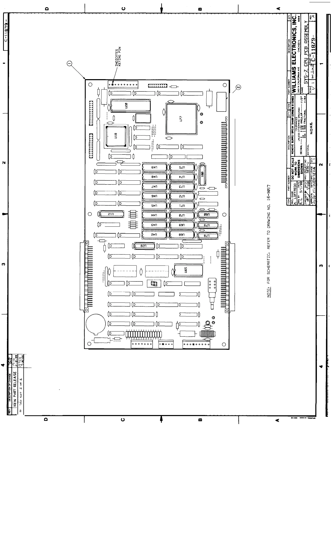
This page is a drawing, shown as the original scan.
A |scveo stem 1S C- 11879 CPU Board Assembly Drawing GAME NAME w3aannNn iuud
WaaWON WALT + JUMPERS REMOVED SEE CHART Pub -|MAGE vss ewer
SEE CHART Ic, PLD-VIDEO ui RAM sea.
SEE CHART Tc, PLD-AUTOERASE 20 eNTL
5340- 12019- 00 IC, RAM/S Les |ssb4 ake
B340- {2213-00 U42 -U49 JIC, RAM/V USB- UTS | 4461 cakKxd
5BBO- HOS@-08 BATTERY ~ LITHIUM, 3V__ BUTTON
SEE CHART, Ic, PLD- COLOR, RAM CNTL. ‘S400- 12220-00 Te, TMS34010 G.S.P.
SEE CHART. Té, PLD-LOCAL CONTROL 5410- 12239-00 IC, CUSTOM ASIC
SEE CHART Ie, PLD-VIDEO RAM CNTU 16-885 LABEL, PCB IDENT.
SEE CHART IC, PLD-ADDRESS DECODE C1878 SYS-Z CPU PCB SUB- ASSEMBLY
TSLEmORCES acess OTeenat speciED ceca “ANGULAR: i BR thio BILL OF MATERIALS
NEW PART RELEASE
See COVER Sa alespaselet
oO a = © N Ree) le) a) Cc Do fe} a Py Q fe} Qo D a ro] ey B fe} a n = ® Q Q a ° io} = are OTE: AN X SUFFIX ARE FORMED FROM ROOT TAMS ELE ELECTRONICS, INC. SIGNALS DRIVEN THROUGH SERIES IFORNIA AVE OWEAGO IL
RESISTORS.
cesenoronoroomce | S| NEW PART RELEASE. See COVER Sar
al oO oO are = © NI o ie) me} Cc wD fe} a Q Q fe} =] ay B fe} a a n az ® o) nD ° i= =
NEW PART RELEASE,
SEE COVER Sut
Lo} a4 a © N o lo) vu Cc w fe} a Cc Qa =] D> a = s = D fe} a = n = 7 oy ® Q o ° = a" a & mo} 2 EPEREEEEEI
i
pase EEEREEEEL
SCRE rc bil Cm
[ [Wen Par RELEASE [Disa] = aaa. A] see cover sur IRR EEEEERERE!
° a = foo} NI o (9) Bo} c o fo} a & Q. fo} =] > a 2] ety BQ fo} a a a za oO oO @ oo fo} i = WILLIAMS ELECTRONICS, INC.
NEW PART RELEASE.
SEE COVER SHT
Oo ane = © NI rte) [?) vu Cc wD fe} a c ° a fe} o ay a n = o Q a ° oe = =
Sa
fee] | _ [NEW PaeT RELEASE,
a
See cover sur
EEEEERERS EEPEEREG!
QO ae = o NI oO ce) vu Cc wo co} oY) = a i fo} a re) Qo & co) fo} a = (7p) a ® @ & ron ioe = a
Srey eras “ONI‘SOINOHLOaTa SW ROeTESS
= aa to} KR a fay o xo n = a fo} a & D & a D fo} pa ce} o fo} a 2D oo [S) a i cs) = ve Oo ASVaTSS Liv MaN
2? a = @ N rte) le} vu Cc lve] fey a : 9° 2. fo} is) D> Qa =| s G fe) a = an za ® Q coe) g = a
| [NEW PART RELEASE, i a3
fo} are = @ N © OQ U Cc les] fe} x a S a iw} > a ( Board 1, Sheet 9 of 11)
ea apse coer eo Ps Bs
Oo are = © N e) uU Cc lve fe} a Cc ° oD D Q a ay aby SS a 2.8 2x
(Board 1, a g
Sheet 10 of 11) a ILLIAMS ELECTRONICS, INC. CAUFORNA AVE HAGE w coon
[o) are a © N ree) @) uv S D fe} a & a fo) =} D a B fe} » a ar n az ® ® & an a fe} =a = a ELEC EE ddsananatan RE i Ba : das aanataanamaeaal Fe
stuieal S| ot EI ot scsi
g Haass stctiss gBassenteagcagsenensnucesssessesg
Py EEEEEEERE EEE OEEEE EEE STS EEE
| ee | x BEER EES rr EB
aecanaeaaaad a
a Et 3)
aaatiad 4 s§basReneeeddaesesseseunssssseseeg dae EM
HI
-Z CPU BD SCHEMATIC
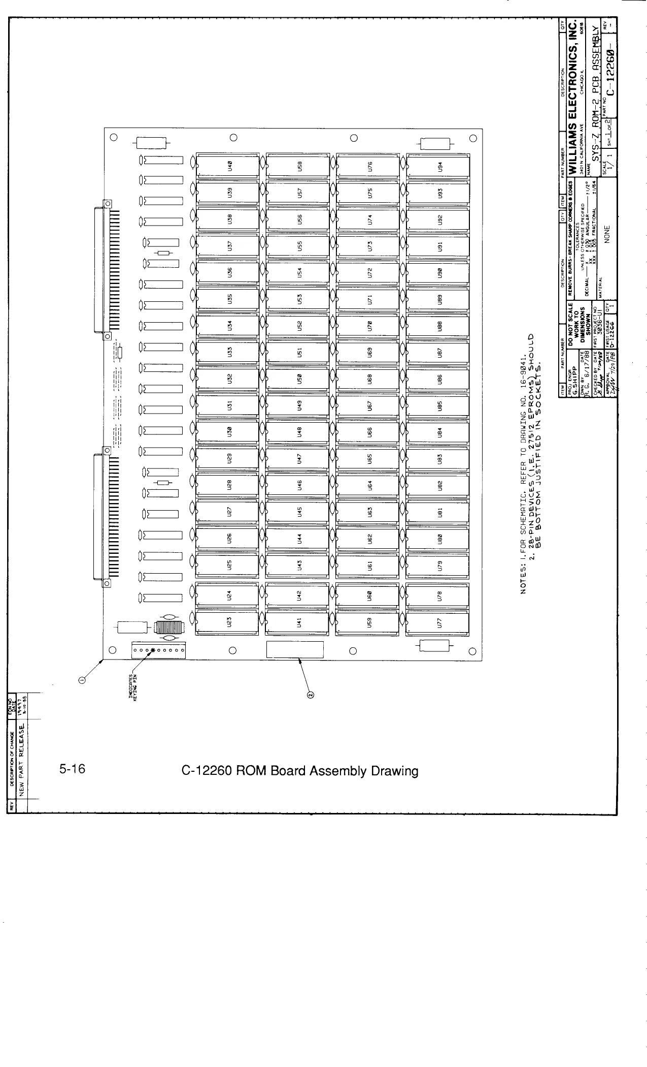
This page is a drawing, shown as the original scan.
NEW PART RELEASE | (7 aa zo=OWa
a<cr 2>=0um
Q<cr Z5sOuc aaah Quonezarnoz
a<Gr QuMNnOUZarnoz
a<ar QuMmeZzarnoz aQ<ar ZsOWm
aaa 2 SaWe adar QUMMOZarHOZ
Q<cr GQuOneZzaHoZ SEE CHART | SEE CHART. GAME ROM SET
46-0050- Ey LABEL, PCB IDENT core264 SYS-2 ROM 2 SUB-ASSY PART NO. [PART DESIGNATION DESCRIPTION
BILL OF MATERIALS
NOTE: FOR SCHEMATIC, REFER TO DRAWING NO. 18-9041
WILLIAMS ELECTRONICS, INC. | HOON CAUFORNA AVE CHICAGO cose
SYS-Z ROM-2 PCB ASSEMBLY
“ONI “SOINOULOI73 SWVITIM S55 «BraRCD ans veawe-suipe arORaW | FWOS LON 00
‘ane wOow aoun0s By Toowr arts 3 oy
ay 2}
of oF VES WHE SPESWHL Ciarrrs zen ‘en orn Sha waay JVM). 1, sna WOOy BovHT
TH. SN@ WOO 3OWRE
SISRS gb a was We. en
C-12260 ROM Board Logic Diagram (Board 2, Sheet 1 of 7) TwaSWrL Coals en
al “ASVA1a8 L8¥d M3N
[Rew ewer RELEASEIESS | aaffejalsorny
ve vs Faasoas PaaLs2as PROGRAM DATA BUS
,s000ur..co = TOEN.H = TOEN. IMAGE DATA BUS
[e) a Ny nD ad fo) aD ce} = ® fe} a c ° 2. fo} go & s B fey a i) n P= is ® Q g iN ° ok a
NEW PART RELEASE | ~1R0E T1541
S1seu. Tan AIROE. 1454 SISEL TH SIROE. Tat. STADE T3C. ~1ROE.174 SIROE_ Te =IROE TSH SIROE Tate SIRO TaW =1ROE TaN SIROE. Take SIROE_TOH. =180E.174 =IROE. Tet =thoE “750 SIRQE Ta SIRQE “Ta SIROE Tee SIROE Ta, =IROE TOL
oO ae i} iN o ro) Dv [e} = lve} ° a c ey Q, fo) o D a » is) Soy a Nd n za Q ° Q pave 13 =PRDE_T: fer) SPADE TY
cag
LOCAL ADDR BUS emo DECEPTION omens o tous WILLIAMS ELECTRONICS, INC. HOIN CALEORNA AVE nica ot
LOESCRIPTION OF CHANGE
|__| NEW PART RELEASE |.
[o) ar ey IN) ® fo) Dv fe) = ive} fey a c 9° Q o D a ry B fey a a) Sheet 4 of 7) [ei otee| eae |
soorce arse
C-12260 ROM Board Logic Diagram (Board 2, Sheet 5 of 7 soorse a ersee
[Fea | aSva7se wavd man] |
oovoNs vou “ONI‘SOINOYLI373 SWVIT CORTES
voore
< © = © ® = n va @ cS) a E @ © > & a fo) a Z w a = fe) ae ° © ql a Oo so0sce etme
[Pet Tasvaiae save wan] J
[a] Woe-71,, et] ro "ONE SOINOULD373 SWVITUM [aan
e “ A s , & 70H er
C-12260 ROM Board Logic Diagram (Board 2, Sheet 7 of 7) [Hava [asvavse ava man |_|
3J2 Functions Pin/Function 1-NC 2-NC 3-NC INDICATES 4-NC KEYING PIN
5 - Key 6 - Memory Protect 7 - T/B Strobe 8 - Player 2 Start 9 - Player 1 Start
Cc. J3 JS eoooocKooO 6 e000 a KOC O O rey
(e) CURE) Rca) ur tf us %f
3J4 Functions /Function 1 - Player 1 Rocket 2- Player 1 Jump 3 - Player 1 Fire 4- Player 1 Crouch 5- Player 1 Right 6 - Player 1 Left 7 - Player 1 Down 8 - Key SO4a— ct CAPACITOR. 182 MFO.
9- Player 1 Up sas 10-Ground ee0-20 8 CAPACITOR, 8.01 MFO. 'S818- R RESISTOR. 8991-00 1 4. 7Kke_1/4W) SX 3J3 Functions ‘S060- ISCRI, SCR2, SCR3) SIP. 10P 8-RES/8-CAP Function 19396-00 | sac4,SRCS _|NETWORK, 4.7K, 470 PF|
S551- Li INDUCTOR, 4.7 UH 1 - Player 2 Rocket 9822-00 7 SS11- 74HC138,_H-CMOS 2 - Player 2 Jump 10848-20 a 378 DECODER 3 - Player 2 Fire 5317- ue |74flse45, ALS TTL 4-PI 2 fh 12208-20 OCTAL BUS TRANSCEIVER
- Player 2 Crouc! S311- Us 74HC3@, _H-CMOS 5 - Player 2 Right 10945-00 QUAD 2-INPUT OR GATE Sari= Ul, U2. U3, |74HCS41, HC TTL 6 - Player 2 Left 12287-00 U4, US OCTAL BUFFER 7 - Key bare BARE PC BOARD
12265-00
8 - Player 2 Down NOTE: FOR SCHEMATIC. REFER TO DRAWING NO. 16-9028. 9 - Player 2 Up Pant No, | PRT OESTONETION DESCRIPTION 10-Ground BILL OF MATERIALS
or
er LABEL, PCB IDENT, Pa CONNECTOR, 64P EURO- 12826-20 OIN CARD CONN, FEMALE| 5791- CONNECTOR, 1@P MOLEX. 10862-10 JS 156" CENTER PINS S791- iH CONNECTOR, 4P MOLEX, 19862-04 156" CENTER PINS
5043- 39 245-00 CS CAPACITOR, .@@1 MFD.
12037 I/O Board loo 000 coo Kor
Board 3 ) iia = ° ° ° ° ° td ° = ° ° ° ° * o ° e)
Assembly D rawing |"rmone ro. ets eee ELECTRONICS, INC.
sé
an x) @ N = [e) D fe} a B ° g a fe} Q > Q =| ray Ee DeSGRPTON iT LIAMS ELECTRONICS, INC. EALEORWA AVE CHICAGO coo “ SYS-Z 1/0 SCHEMATIC
CPU_INTERFACE,
B2-¢ = weiBeIq Bul)py-semog
c0-seag0-20r5 Wa axis BHM (20+P¥060-L10S Na BoLSIHA “Gavoe a>
Qa * Le) L ce: n = = s =] a Uv fo} oO @ n i<j mel os. > n o QO S < iw) o =. =] a 2485062526002 aBOBOROBOReko8 OGQGOROGOGOSO SPOLEL86L5°O ABOSOGOGOSE 92620080 AGOGOKOGO 202626) QSOGOKO enente) Q50g80 Q50 % 1o-85ar101 LABEL -HIGH VOLTAGE 4008-01008-O4 te ‘5-40 1 Vg PPR
20-9574 PIS SWicHER
FASTNER BUTTON
SHIELD - SW POWER SPLY
BRKT - Sw POWER SPLY
TPSWER INTER PCB
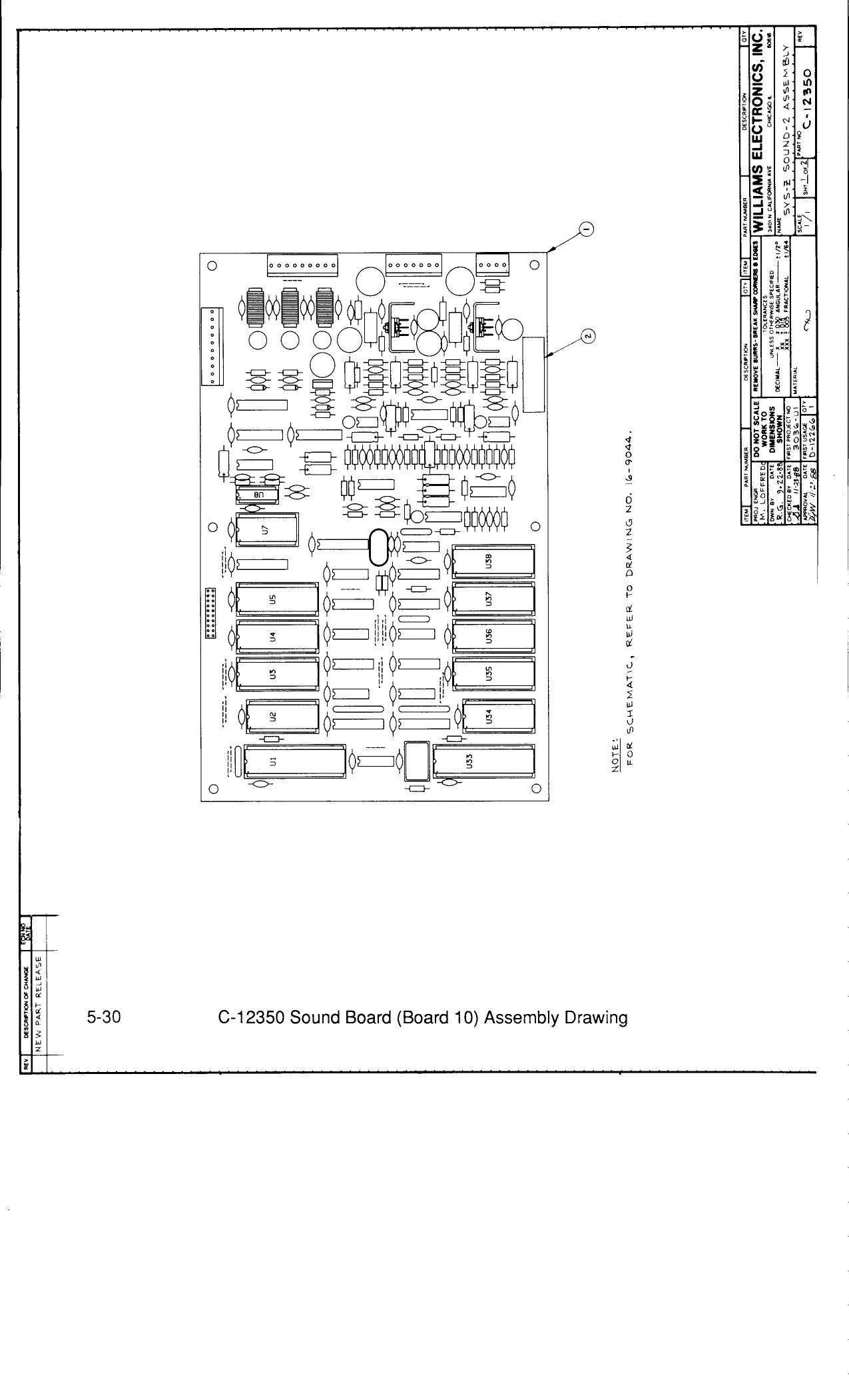
This page is a drawing, shown as the original scan.
[o} a Ny o a fo) n o & a a les} a G D a = RS) c & Q, i) ie) D a a Ry
REFER TO DRAWING NO. 18-9044
3, 04,05, U35 see want | 3,04 U5. U3 27st2/: ROM 250 NS. YH3012 QUAL SERIAL OAC ‘yH2151 SOUND GENERATOR Ok X 8 STATIC RAK, 150NS LABEL, PCB IDENT
c-12950 SYS-2 SOUND BOARO SUB-ASSY
FanT_wO_ [Pant veSTGNATION DESCRIPTION
BILL OF MATERIALS
ue 27512 om 274001
us Banose
ia ia i ii F fe
23, vatsa74 Tee ree] rearraec —- aaron
DESCRPTONOF CHance__| “ET | NEW PART RELEASE,
- 9047#F R87 r ‘O0320F DescnaTON MS ELECTRONICS, INC. IA AVE ‘cHicAgo «| for % SOUND-2 BD SCHEMATIC
Weave ‘SOINOYU.LI373 SW!
aaTTOR zr eae corer? v cocen een tw Yo ise ad 005
* T coren eocen) a tw ‘oe he
“ASva13e avd Man] | a ET
INEW PART RELEASE
Rae : le. i 54 ee
i ry WOLExo? Pry ker
te 4000 MF us WOLeKo4 VOLUME WILLIAMS ELECTRONICS, INC. SHO1N CALFORNA AVE CHCAGO K 060
| [NEWPART RELEASE] | ws RESET Rr@BON20
TROBE. pac. vss ac vAEF. WILLIAMS ELECTRONICS, INC. {HON GALORI AVE ConcAGo cose
INEW PART RELEASE [2/9%,, picares a KEYING PIN 16-8850 LABEL, PCB IDENT. -216 , - S791- rT CONN., 1O-PIN MOLEX, 10862-10 156" CENTER PINS. Sq91- be CONN., 7- PIN MOLEX, (0862-07 56" CENTER PINS: 5191- U3 CONN., 2-PIN MOLEX, 108G2-02 5G" CENTER PINS Bozo-o) | FlF2,F3 [Fusenouver
5130- 69797- 00 Fa 5731-10356-00 F2 _ |FUSE 3A, 250V 5731-09128-00 F1 _ | FUSE 2.5ASB, 250V 5040+ © CAPACITOR, ELECT, 12313-00 2 RAD., 1500 MFD, 25V. So40- 7 CAPACITOR, ELECT, 123\4-00 RAD., 2200 MFD. 28v. S67\- LIGHT EMITTING O9019-00 | SEDI LED2 [Diove, RED
S100> aga 16-00 BRI BRIDGE RECTIFIER, 35v, FUSE, 0.15A, 250V
C-12218 Sound Power Supply Assembly Diagram SO70ee ae DIODE, IN4001 5O10- RESISTOR, <r, 09314-0090 UL 2K S%o Yq WATT
5773- 12309-00 BARE PC BOARD
NOTES’ 1. FOR SCHEMATIC. REFER TO DRAWING NO. 16-9037. 2, ALL FUSES To BE INSTALLED AFTER SOLDER WASH.
- EACH FUSEHOLDER CAN BE SUBSTITUTED WITH 2 FUSE CLIPS PT, NO. 5732-09118-00. 4.BR1 MUST BE MOUNTED /" ABOVE SURFACE OF PCR, DESCRIPTION
3036-U Son ae fee Yy tintes | e-12259|
[ [NEW PART RELEASE [7/99] 20.0vac|
- 0vAc| qgbeeveee] TU]
[o) =i iS} x} ie Cy n ° Ee a a D = o n < acs < n ° > ® oO ie} @ Fey
SOUND POWER SUPPLY E etn tee|
INTER- FACE BOARD
INTER- FACE BOARD
CPU BOARD 14J3 Loe te
R con
CCOIN L COIN SLAM VAULT ADV
ADVANCE
NC KEY.
P/O 3J2
GERMAN BIT- FRENCH BIT-
jumper MEM PROT-
P/O 3J4
MEM Fe: o
Oo=- nk WDhM = 141P.
P/O 3P1 2 va
i WHT-YEL. H WHT- WeT-GEN LT war-stu | fled [| WHT. RY OMDNONA WD =
Cabinet Wiring Diagram 8P2 8J2
10J5 10P5
BOARD PARALLEL CAUTION: Don't
substitute a 5K, iw] Bae aa RESISTANC ; pinball pot. 10J4 10P4
| U32 OUT | 1 [> | |-Be0-BLK |
@o GRN-BLK
| SOUND | JMPR SLCTD | 3 | \o-|_RED-VIO | |
| BOARD | @oD | GRN-VIO | |
| U4 OUT | 3 |Z | [-RED-BLU | |
| fen) | 5 | 6P2 | . |
a P/O 5 5
| INTER-| | PL 1 | 32 | 3P2 | Capacitive |
| FACE | START | 9 | 7P1 | apace |
poanp | PL2 8 START NV NN
| PLAYER 2 LEFT | 6 | YEL-BLK | \\ | |
| PLAYER 2 RIGHT | ® |S [fveuaan [S| | VO_ | 975s | |
| INTER] BLAYER 2 CROUCH | a [>] yeu ReD | NN | 7SW5, | |
| reo] | PLAYER 2 FIRE | 3 [> +L YELORN | NN | 75W6 |
| PLAYER 2 JUMP | > [>| LyEL-vio | \\ | 7SW7 | |
| PLAYER 2 ROCKET | + |S LLYEL-GRY_| | N | 7swe | |
| PLAYER 2 DOWN | 3 | lol | \ | |
| PLAYER 2 UP | oa all | \N |
SOUND POWER AC RETURN ‘=i 2"
SUPPLY 6.3VAC te] 1
| ceo 4 | 4 | WS |
| PLAYER 1 UP. | is | N |
INTER. | PLAYER 1 DOWN 9 |S LOnnpan [Te
| PLAYER 1 LEFF | ORN-RED_|[> | NN | |
| es | r 1E| §(3ran | TEN | |
| poarp | PLAYER 1 RIGHT | [aot | N | |
| PLAYER 1 CROUCH | 3 SL Onn ve | TENN | |
| PLAYER 1 FIRE. | [ORN-GRN_|> | NN | |
| PLAYER 1 JUMP. | ; | ORN-BLU | N |
| PLAYER 1 ROCKET. | 4 | ORN-VIO_[S KY | |
| KEY | s{St | 7 |