Gridiron Fight
Gridiron Fight (World) (Tehkan, 1985) · Manual · 42 pages · 36 sections · original scan
Operation Maintenance And Service Manual
CONTENTS
- SPECIFICATION «cna 00» macaw sree Seite tts GLeek BEYER w Se 1
- WARNING ... eas 2 BD, GAUTIONS oes cavewns crnnawge ceases serene ner eetnes 3
- HOWTO PLAY 2200. 2 cence creme mae see memes 5
- HOW TO REMOVE MAIN PCB ............-. 0s ee cece eeeeees 6
- DIP SWITCH occ messse SS 5 ceene op casa one Sang cod pwns 7
- SELP TEST acne uxaua cos ganas es iovaina peeceases vamee aa 9 S, MAINTENANGE. wesc o. ccssaisie oes angie vies genes cen sewage s 10
- TROUBLE SHOOTING .... 2.0... . cece cee cece cece ee nnee 11 10; ILLUSTRATED PARTS LIST cas sci nemcird sre steeds sears 13
- SCHEMATIC DIAGRAM ... 22200. seamgwrs 60+ nam cee ep eee rs 18 12, MAIN PCE LOCATION ... wer ey sess vwewe sh ammge cee ceey ve 19
- MAIN PCB PARTS LIST ......... 2... e cece eee eee e eee eeee 20
- POSITION OF CONNECTOR .........- see e cece eee e eee ee 21 1S: WIRING ..000% swans cos renee (8s eee 063 > TREES Oss ead ts 21 16, BLOCK DIAGRAM 55 5.22008 onveesscceereetecessarwems 22
CRT MANUAL
- PRODUCT SPECIFICATIONS ......... 0... es eeee cece ences 23
- IMPORTANT SERVICE SAFETY INFORMATION ... . 26
- HOLD-DOWN OR SAFETY CIRCUIT INFORMATION - 27
- CAUTIONS ON USE ...............006- 28
- ADJUSTMENT AND CHECK PROCEDURES . . 29
- TIMING CHART ............2-e eee eee - 33
- OUTLINE OF ASS’Y PCB UNITS . 34 8 WIRING DIAGRAM .....050cscseewscresseavewsces . 34
- ASS’Y PCB MAIN PARTS LOCATION -. 35
- CRT DISPLAY ASS’Y PARTS LIST ............00 0 eee eeeeee 36
- CRT SCHEMATIC DIAGRAM ........... 22 cece cece cece eee 37
LIST OF ILLUSTRATION
Fig. 1 External Dimensional Drawing ... 2... 0.6.6.0 eee ee eee eee ene 1 Fig. 2 EMI Shield PCB & EMI Cage... 6.6... eee cece eee 6 Fig. 3 Switch Panel 2... 0... ec cece eee eee eee eens 6 Fig. 4 Position of DipSW .. 1.0.6.0... eee e cece teens 7 Fig. 5 Self Check... 2... cece cee eee eee teens 9 Fig. G Crosshatch 2.0... 06. c cece ee eee eee eee teen renee 9 Fig. 7 Blade Adjuster 2.2.2... ccc cc cee eee eter eee enees Fig. 8 Cabinet Ass'y.. . Fig. 9 Control Panel Ass’'y........ 00 c ee eee eee eee eee eens 15 Fig. 10 Control Ball Ass'y 0... cece cette 16 Fig. 11 Power Supply ......... 0c eee eee eee eee eee nee 17 Fig. 12 Power Board Schematic Diagram ....... 0.0.00 cece eee eee eee 18 Fig. 13 Credit Control PCB Schematic Diagram ............. 00.000 e eee 18 Fig. 14 Switching Regulator Schematic Diagram . . 18 Fig. 15 Main PCB IC Location —1 . 19 Fig. 16 Main PCB IC Location —2 . . 19 Fig. 17 Position of Counter . . 2 Fig. 18 Wiring........ . 21 Fig. 19 Block Diagram... 2.2... cc eee eee eee eee teen eee 22
CRT MANUAL
Fig. 1 Hold-down Circuit Diagram 2.0... 0... ec cece eee eee tenes 27 Fig. 2 High Voltage... 0... ccc cece eee ee eee eees 28 Fig. 3 High-temperature Section... 2.0.00... cece eee eee eens 28 Fig. 4 Connection Diagram... 0.0.2... ec ee eee ene 29 Fig. 5 Purity Adjustment—1 ....... Subd seeewewaes one tees eee 31 Fig, 6 Purity Adjustment —2 2.0.0... ccc cece cece ee eee eee 31 Fig. 7 Purity Adjustment—3 ......... 0... ccc eee eee 32 Fig. 8 Static Convergence Adjustment —1........... 0.0... e eee eee 32 Fig. 9 Static Convergence Adjustment —2 ......... 0.2... cece eee eee 32 Fig. 10 Connection Diagram ..... 0... eee eee tee cena 33 Fig. 11 Horizontal Signal 2... 2... eee eee eee eee 33 Fig. 12 Vertical Signal 20... ec cee eeee eee eae 33 Fig. 13 Out Line of Ass'y PCB Units.... 22.2.0... cece cece eee eee eee 34 Fig. 14 Wiring Diagram 2.2... cece cee tenes 34 Fig. 15 Ass’y PCB Main Parts Location... ....... ccc cece eee ee eee 35 Fig. 16 CRT Schematic Diagram... 1... 0... cece eee eee teens 37
= TEHKAN
1. SPECIFICATION
e@ Power supply 115V AC
e@ Power consumption 100W
© Weight 209 1/2 Ibs
37% inch
—39% inch = <————27 inch >
Fig.1 External Dimensional Drawing
2. WARNING
AWARNING A
Use of non-TEHKAN parts or modification of any TEHKAN game circuitry may adversely affect the safety of your game, and may cause injury to you and your players.
This equipment generates, uses, and can radiate radio frequency energy and if not installed and used in accordance with the instruction manual, may cause interference to radio communication. It has been tested and found to comply with the limits for a Class A computing device pursuant to Subpart J or Part 15 of FCC Rules, which are designed to provide reasonable protection against such interference when operated in a commercial environment. Operation of this equipment in a residential area is likely to cause interference in which case the user at his own expense will be required to take whatever measures may be required to correct the interference.
Players may receive an electrical shock if this game is not properly grounded! To avoid electrical shock, do not plug in the game until it has been inspected and properly grounded. This game should only be plugged into a grounded 3-wire outlet. If you have only a 2-wire outlet, we recommend you hire a licensed electrician to install a grounded outlet. Players may receive an electrical shock if the control panel is not properly grounded! After servicing any parts on the panel, check that the grounding clip is firmly secured to the metal tab on the inside of the control panel. Only then should you lock up the game.
Before connecting the game to the AC power source, verify that the proper voltage-selection plug is installed on the game's power supply.
To avoid electrical shock, disconnect the game from the AC power source before removing or repairing any part of the game. When removing or repairing the video display, extra precautions must be taken to avoid electrical shock because high voltages may exist within the display circuitry and cathode-ray tube, (CRT) even after power has been disconnected. Do not touch internal parts of the display with your hands or metal objects! Always discharge the high voltage from the CRT before servicing this area of the game. To discharge the CRT: attach one end of a large, well-insulated, 20-kV jumper to ground. Momentarily touch the free end of the grounded jumper to the anode by sliding it under the anode cap. Wait two minutes and discharge the anode again.
= TEHKAN
3. CAUTIONS
(1) Care in Usage Care should be taken to avoid dragging or dropping the machine when transporting to prevent damage to the CRT. e Use fuse of indicated rating. e As high voltage is present in the monitor and TV PCB, adjustments or repairs should be left up to
(2)
(3) a serviceman and should never be touched by the layman.
Care in Handling Always turn off the power supply switch before handling. Avoid inserting and pulling the plug in rapid succession. Do not check the IC board circuit with a tester. Avoid rough handling in transportation; the picture tube is fragile.
Installation e As the video game is for “indoor use’’, do not install outdoors. e When installing, avoid the following places.
- Near indoor pools or showers
- Where leaks exist
- Under direct sunlight
- Near heaters or other heat emitting devices
- Near hazardous items (volatile fluids, gas cylinders, etc.)
- Where vibrations are severe (near construction sites where jack hammers, etc. are used.)
- Inclined places
- Near fire extinguishing equipment
- Near emergency exits
- To prevent electric shock do not use this (polarized) plug with an extension cord, receptacle or other outlet unless the blades can be fully inserted to prevent blade exposure. In case the machine does not work properly after the power switch is turned on, make sure the proper voltage exists at the line cord.
Trouble Shooting When it is believed that trouble has developed, always confirm the following items.
Is the fuse intact? (Always use fuse of the designated rating.) When the replaced fuse burns out again, this will indicate that another component is defective. Are there any poor connections (connectors) or open circuits? Special care must be taken to ensure connectors are firmly inserted. Troubles due to faulty contacts can be considered from various sources,
Reorient the receiving antenna Relocate the computer with respect to the receiver Move the computer away from the receiver Plug the computer into a different outlet so that computer and receiver are on different branch circuits.
If necessary, the user should consult the dealer or an experienced radio/television technician for additional suggestions. The user may find the following booklet prepared by the Federal Communications Commission helpful:
“How to Identify and Resolve Radio-TV Interference Problems”. This booklet is available from the US Government Printing Office, Washington, D.C., 20402, Stock No. 004-000-00345-4.
= TEHKAN
4.HOW TO PLAY
- How to Play e 1 Player — Player vs computer e 2 Players — Player vs opponent
e Control your player with the Controlwall!
1st Player (Red-team) es
Pass : 2nd Player (Blue-team) es
After selecting pass play, move OB to passing position, press Pass Button and rotate Controlball in the direction you want to pass. In Kick Formation, rotate Controlball for kick and direction. Kick :
- Even when your player has disappeared beyond the screen, if you turn the Controlball,
according to the direction indicated on |<
in the lower right part of the screen, you can return the disappeared player to the screen,
© Choose the Formation during huddle With the Controlball, choose the desired Formation No., and press Formation Set Button.
Present Position Run Formation #o1s asnasaa
Pass Formation Kick Formation
- Techniques ¢ Run play (Formation No. 1 ~ 4)
Offense formation No,— -MLB (middle line backer)
—Runner course (quarter back) — Defense formation No, e For run offense Move QB in the direction indicated by selected Formation! (You can’t pass.) e For run defense Limit QB’s advance by selecting Formation No. your opponent is likely to choose!
e Pass play (Formation No. 5 ~ 8)
-MLB
7 Receiver
—Runner course
© For pass offense After snap, move OB to desired position, locate the receiver you wish to pass to, press Pass Button and rotate Controlball in the direction of receiver. e For pass defense Controlball controls MLB, you can blitz or drop back for pass interception.
e Kick play (Formation No. P, F)
PUNT KIC
FIELD GOmL,
e Kick Select punt or field goal according to offensive strategy.
5. HOW TO REMOVE MAIN PCB
{1) EMI Shield PCB & EM! Cage © By loosening the screws (A) (four places) extract the EMI cage.
© By removing the screws (B) and (C) (four places each) extract the EMI shield PCB and the main PCB.
EMI Cage
Main PCB EMI Shield Plate
EMI Shield PCB
- Switch Panel Description
a yo [ fo Ce oS Fig.2 EMI Shield PCB & EMI Cage
Sound Volume Service SW Power SW
Service Switch Panel
Fuse (3A) Demagnetizer SW Coin Counter
AWARNING A Use of non-TEHKAN parts or modifications of any TEHKAN game circuitry may have rable effect upon the safety of your ‘may cause injury to you and your Fig. 3 Switch Panel
= TEHKAN
6. DIP SWITCH
e Position of Dip SW
oo 5902 — XA
Sound volume
MAIN PCB When removing PCB, refer to Fig. 2 Dip Sw2 Dip swt sal on page 6. ~a ON 1~8 orp Dip SW3 OFF
Fig.4 Position of Dip SW
e Setting for Dip SW
| 1 | 2 | 3 | 4 | 5 | 6 | 7 | 8 |
Dip SW1 Unused
| . | Coin/credit | Defense huddle | it | ||
| Dip SW2 | TP | 3p | time | Count down | Huddle time |
Demon-
| Dip SwW3 | 1P Game time | 2P Game time | 2P Extra time | stration |
sound
© Dip Sw2 © Coin/Credit
| 1P. | 2P | (*Refer to extra time per coin.) | |
| sw | 1 | sw | 2 |
te 2P
| 1Coin | 1 Play | OFF | 2Coin | 1 Play | OFF |
| 2Coin | 1 Play | ON | 1Coin | 1 Play | ON |
Defense Huddle Time
| SW | | | Huddle time for defense can be set after of- | |
| Defense | 3 | 4 | fense’s formation setting. |
| huddle time | -. | . | Se |
- Game starts with the formation number indi-
| Huddle time. | BEF | OFF | cated at the time after this setting time has |
| 5 Seconds after offense's | ON | OFF | passed. (Refer to huddle time) |
formation setting
| 3 Seconds | " | OFF | ON |
| 7 Seconds | a | ON | ON |
e Count Down
| sw | "| | Speed of the count down for game time can | |
| Count down | 6 | 8 | be set. |
| 1 Count 1 Second | OFF | OFF | |
| " | 50/60 Second | ON | OFF |
| = | 54/60 Second | OFF | ON |
| "87/60 Second | ON | ON | | |
e@ Huddle Time Sw Huddle time can be set.
| Huddeane— | 7 | _ | 8 | Game starts with the formation number indi- |
| 15 Seconds | OFF | OFF | cated at the time after this setting time has | |
| 10 Seconds | ON | OFF | passed. (Refer to defense huddle time.) | |
| 20 Seconds | OFF | ON | ||
| 25 Seconds | | | _ON | |___ON | | |
© Dip SW3 e@ 1P Game Time @ 2P Game Time (*Refer to extra time per coin.) sw sw 7}
| 1P Game time | 1 | 2 | lem | 3 | 4 | : |
| 1:30 | OFF | Orr | | | 2: 30 | OFF | OFF | OFF | |
| 1: 00 | ON | OFF | 1: 00 | ON | OFF | OFF |
| 2: 00 | OFF | on | | 1: 30 | OFF | ON | OFF |
| 2: 30 | ON | ON | 2: 00 | ON | ON | OFF |
| 3: 00 | OFF | OFF | ON |
3: 30 on | OFF | ON |
| 4: 00 | OFF | ON | ON |
| 5 : 00 | ON | ON | ON |
e 2PExtra Time (*Refer to extra time per coin.) SW | Time is increased for 2P game when additional
| 2P Extra time | 7 | 7 | coin is inserted, Also extra time can be set in |
| 1:00 | OFF | OFF | addition to the normal game time. |
| 0: 00 | ON | OFF | One half of time allocated will be added for |
| 0:10 | OFF | ON | each coin, when using 2 coins equal 1 play. |
| 0: 30 | on | ON |
2 coins 1 play (2P game time) + (2P extratime) + 2
1 coin 1 play (2P game time) + (2P extra time)
®@ Demonstration Sound SN 8 Demonstration sound Sound OFF No sound ON
= TEHKAN
7 SELF TEST
- Self Check When turning power ON, checks are conducted in the following sequence.
@ ROM/RAM/Color Checks When each of these checks is O.K., it is displayed for 4 seconds, then followed by the next display. lf any of ROM and RAM is ERROR, repeat checking. The color pattern is also displayed at the same time. At this time, when pressing PASS & FORMATION SET button, it continues to be displayed, so conduct color adjustment.
Then, cross-hatch is displayed for 4 seconds. At this time, when pressing PASS & FORMATION SET button, it is displayed. When pressing again, a demonstration screen will follow.
8. MAINTENANCE
- Push Button Blade Switch e Adjust the blade switch contacts for correct gaps. When the blade is bent, straighten it by using the blade adjusting rod.
AWARNING A To prevent an electrical shock hazard, unplug the game prior to performing any maintenance.
Fig.7 Blade Adjuster
e Take out carbon deposits on the blade switch by using a clean cloth, etc.
- Inspecting the Controlball @ Check the controlball to see if its roller shafts have worn. In case there is too large a clearance between the C.B spacer and the bal! due to the excessive wear of the roller shaft, replace either the roller shaft A or the roller shaft B. e Lubricate the control ball’s ball bearings every month or 2,000 credits. After wiping out dust, etc. cleanly, place 2 or 3 drops of light duty oil on each of 6 ball bearings.
= TEHKAN
9. TROUBLE SHOOTING
(1) When the power switch has been turned ON after inserting the power plug into the outlet, no action ensues Check if the power source voltage is 115 V. e Check if the plug has been normally inserted. © Check if fuses have blown,
(2) When the power switch is in the ON state The controlball lamp and the coin slot lamp do not come on.
- Check if the filament is off.
- Check if voltage in the secondary side of the insulator-type transformer is normal at 12V AC.
- Check each connector if its contact is normal.
No image appears on the CRT
- Check if the CRT heater is glowing.
- Check if power is supplied from the secondary side of the insulator-type transformer.
- Check if the CRT itself is malfunctioning.
- Check if the main PCB's 5V power source pilot lamp is lit, and 5V is being supplied from the DC power source.
Images appear on the CRT, but the action seems to be incorrect.
- Check if the main PCB is supplied 4.5 ~ 5.5V of DC voltage.
- Check if there is improper contact between 3 CPUs (Z80A) on the main PCB 5902-XA and the IC 40-pin socket.
- Check if there is improper contact for the J5 connector (see Fig. 16).
After turning power ON, ROM-RAM check is displayed on the video displays. In case any ROM or RAM fails, replace it as per the table below.
| Device No. | | | Part number | Device No. | Part number | ||
| | | RAMO | 5902-XA | 5C | ROM 0 | 5902-XA | 3A |
| RAM 1 | 5902-XA | 9D | ROM 1 | 5902-XA | 3C | |
| RAM 2 | 5902-XA | 9F | ROM 2 | §902-XA | 3D | |
| RAM 3 | 5902-XB_ | 6P | ROM 3 | 5902-XA | 9C | |
| RAM 4 | 5902-XB | 6E | ROM 4 | 5902-XA | 8R | |
| RAM5 | 5902-XB | 5A | ||||
| RAM 6 | 5902-XA | 7HJK | ||||
| RAM7 | 5902-XA | 9R |
-W-
The cross-hatch on the video display is not normal.
- Adjust the knob for voltage supplied to the CRT, and the CRT’s horizontal and vertical sync. knobs,
The game is not credited even when a coin is inserted.
- Check if the coin is stopped up.
- Check if the coin mechanism or the coin micro-switch is malfunctioning.
- Check if the coin credit PCB is malfunctioning, or there is improper contact for each connector.
The coin counter does not work.
- Check if the coin credit PCB is malfunctioning, or there is improper contact for each connector.
- Check if the coin counter itself is malfunctioning.
‘Player Select’ cannot be performed.
- Check if there is improper contact for the push button blade switch.
- Check if there is improper contact for the J3, J2 connectors (see Fig. 16).
The controlball itself does not rotate smoothly.
- Check if there is something wrong with the bal! bearings (see page 10, ‘Maintenance’).
- The controlball ceases to rotate smoothly when there occurs contact between the ball and C.B spacer, due to the loosening of 4 carriage bolts and nuts which fix the ball on the control panel.
The control ball does not work.
- Adjust the interval between 2 photointerrupters of the photo PCB.
- Check if the disc plate is bent, or there is improper contact for each connector.
LED PCB does not light up normally.
- Check if there is improper contact for each connector.
- Replace LED PCB, if the device turned out to be defective by replacing LED PCBs on right and left sides.
Cannot perform ‘Formation Set’ or ‘Pass’.
- Check if there is improper contact for the push bution blade switch, or each connector.
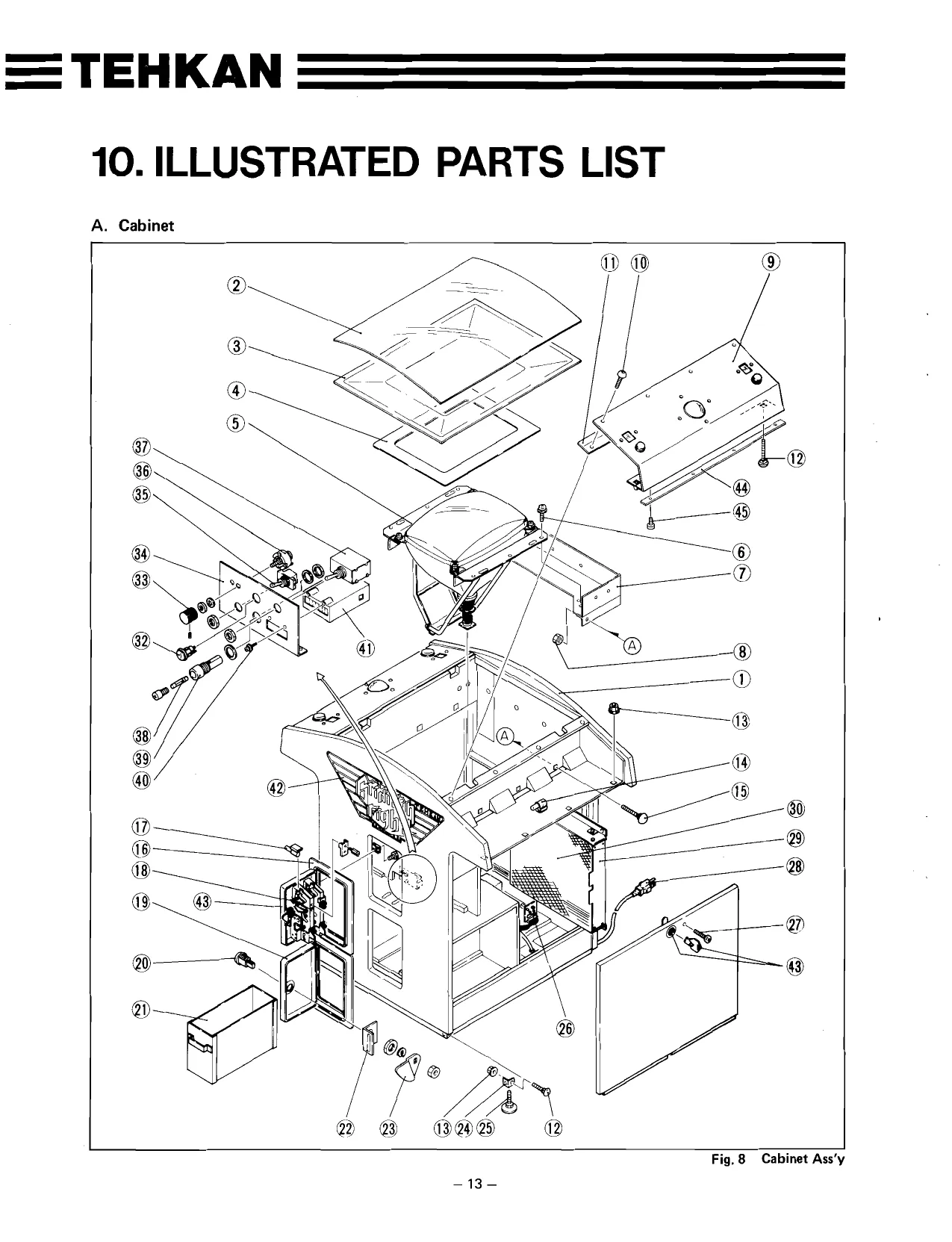
This page is a drawing, shown as the original scan.
Cabinet Parts List
| Nem | Part No, | Description | arty | | nde} | Part No. | Description | a'ty | ||
| 1 | |CA-01-001 | Cabinet | 1 | 20 | AM-02.004 | Lock Ass’y | 1 set | |||
| 2 | |PG-01-001 | Cured Glass | 1 | 21 | AM-01-003 | Cash Box | 1 | ||
| 3 | RF-01-001 | Smoke Shield | 1 | 22 | | AM-01.004 | Lock Cam Bracket | 2 | |||
| PP-01-001 | Instruction Seal | 1 set | | 23 | | AM-01-005 | Lock Cam | 2 | |||
| PP.01-002 | Graphic Seal | 2 | 24 | BM-01-003 | Adjuster Bracket | 4 | ||||
| 4 | |ap-02-001 | CRT Masking Paper | 1 | 25 | BM.01.004 | Adjuster | 4 | |||
| 5 | £02001 | | CRT | 1 | 26 | |£-02-006 | | Power Supply Ass’y | 1 |
| 6 | |Ms.02-620 | Machine Screw | 4 | 27 | MS-02-420 | Machine Screw | 1 | |||
| 7 | |BM.01.001 | CRT Bracket | 2 | 28 | £02007 | | Power Cord | 1 | |
| 8 | FIN-02-005 | Flange Nut | 6 | 29 | |€-01-001 | | EMI Shield PCB | 1 | ||
| 9 | AM-01.001 | Control Panel Ass’y (1 player)| | 1 | | | | 30 | AM-01-006 | EM Cage | 1 | |||
| AM-01.002 | ” | (2 player] | 1 | E.01-002 | | Main PCB | 1 | |
| 10 | 8B-02-630 | Button Bolt | 8 | 31 | |£-02.008 | | Speaker | 2 | ||
| 11 | | 8M-01-002 | Glass Plate | 2 | 32 | £.02.009 | Service Switch | 1 | |||
| 12 | CB-02-630 | Carriage Bolt | 8 | 33 | |£.02.011 | | Volume Control Knob | 1 | |
| | 13 | |FNN-02.006 | Flange Nut | 8 | 34 | BM-01-005 | Switch Bracket | 1 | | |||
| 14 | /£-02-002 | | Lamp | 2 | 35 | | £-02-011 | | Demagnetizer Switch | 1 |
| E-02-003 | Lamp Socket | 2 | 36 | £-02-012 | | Volume Control | 1 | |||
| 15 | | MS-02-530 | Machine Screw | 6 | 37 | |E-02.013 | | Power Switch | 1 | |
| 16 | |AM.02.001 | Coin Door Ass’y | 1 | 38 | £02014 | | Fuse | 1 | |
| 17 | \€.02.004 | | Lamp | 2 | | | 39 | (£02015 | | Fuse Post | 1 |
| £.02-005 | | Lamp Socket | 2 | 40. | | s.02-312 | Machine Screw | 2 | ||
| 18 | AM-02.002 | Coin Mechanism (US 25c) | 2 | 41 | |e-02.016 | | Coin Counter | 1 | ||
| 19 | | AM-02.003 | Cash Door | 42 | | PP.01-003 | Side Graphic (Both side) | | 1 set | |||
| 43 | | AM.02-006 | Lock Ass’y | 1 set | |||||
| or aac | cite area tha | ety ob yout | 45 | | MS-02-410 | Machine Screw | 4 |
game, and may cause injury to you and your players, To prevent an electrical shock hazard, be sure to turn the game off before removing or replacing components.
—~14-
= TEHKAN
B. Control Panel Ass’y & Parts List (1st player side}
AWARNING & Use of non-TEHKAN parts or modifications of any TEHKAN game circuitry may have unfavorable effect upon the safety of your game, and may cause injury to you and your players. Fig. 9 Control Panel Ass’y
a Part No. Description Q'ty ie Part No. Description Q'ty
| 1 | | BM-01-005 | Control Panel (1st player) | 1 | 6 | CB-02-435 | Carriage Bolt | 8 | |||
| BM-01-006 | ” | {2nd player) | 1 | 7 | RF-02-001 | Push Button | 4 | ||
| PR-01-001 | Contro! Panel Overlay | 2 | 8 | RP-01-001 | Purple Board | 4 | ||||
| PM-01-001 | Player Panel | 1 | 9 | BW-01-002 | LED PCB Bracket | 4 | ||||
| 2 | AR-01-001 | Control Ball Ass'y (Red) | 1 | 10 | FN-02-004 | Flange Nut | 8 | | ||||
| AR-01-002 | ” | (Blue) | 1 | 11 | |E-01-003 | | LED PCB | 4 |
| 3 | RF-01-002 | C.B. Spacer | 2 | 12 | WS-02-310 | Wood Screw | 8 | ||||
| 4 | FN-02-006 | Flange Nut | 8 | 13° | RF-02-002 | Push Button | 2 |
5 | CB-02-675 | Carriage Bolt 8
C. Control Ball Ass’y & Parts List
players. fades Part No. Description Q'ty
| 1 | RF-01-003 | Housing | 4 |
| 2 | RF-02-003 | Ball (Red) 1 RF-02-004 (Blue) 1 3 | AM-02-005 | Ball Bearing 12 4 | AM-01-007 | Roller Shaft A | 4
| 5 | | AM-01-008 | Roller Shaft B | 2 |
6 | BM-01-007 | Disc Plate 4
| 7 | | MS-02-408 | Machine Screw | 4 | |
| 8 | | MS-02-512 | Machine Screw | 12 | |
| 9 | | E-01-004 | | Photo PCB | 4 |
AWARNING A Use of non-TEHKAN parts or modifications of any TEHKAN game circuitry may have unfavorable effect upon the safety of your game, and may cause injury to you and your
Fig. 10 Control Ball Ass’y
= TEHKAN
D. Power Supply & Parts List
- ® D ® ®
AWARNING A Use of non-TEHKAN parts or modifications of any TEHKAN game circuitry may have unfavorable effect upon the safety of your game, and may cause injury to you and your players. To prevent an electrical shock hazard, be sure to turn the game off before removing or replacing components.
Fig.11 Power Supply
nox Part No. Description Q'ty Ne eX) PartNo. Description Q'ty
| 1 | | £-02-017 | Transformer | 1 | 4 | |E-02-020 | Noise Filter | 1 | ||
| 2 | | E-01-005 | | Credit PCB | 1 | 5 | | £-02-021 | D.C. Power Supply | 1 |
| I | E-02-018 | Credit PCB Connector | 1 | 6 | BM-01-010 | Power Supply Plate | 1 |
BM-01-008 | Credit PCB Bracket 2
| 3 | | E-02-019 | | CRT Connector | 1 |
I BM-01-009 | CRT Connector Bracket | 1
11. SCHEMATIC DIAGRAM
A. Power Board Schematic Diagram C. Switching Regulator Schematic Diagram 4 Noise FILTER [lal
| A Sut (AWGI8x3). CORD | Mao Boas | ! | ||||
| _ | - | 7 | war. | WaT | f | |
| — | - | = | - | SR | GNF ek | ' |
BLK. Li ' I
| — | a | a ry | 1 |
| - | i | owe asesa SM. | j |
| rN | na | | | |
| WARNING: FOR COTINUED SAFETY. RE- | T _—___BLk__ | —4 | ' |
(A DEG S COIL '
| ie nee | | | 2 of | 25 | ||
| oon | 5 | 5 | |||
| Bane #20 ot esa | ED | — | a | ot | ge |
| ——~ er av one | 2 | a8 | |||
| ASN oo | | | 5 i | |||
| 7 | aLu | o 3 |
COI Wide CONTROL PANEL H H
| ALRECEPTACLED | 7 | coe | i |
USE ONLY 5) |
| vibe MONITOR! | iisv | i | |
| = | war | war, | i |
x te POWER SUPPLY ' e|
| ¢ | — | _I | : | ||||
| TO LOGIC PCB | AWG 10x6 | pgrey tf ——S | 2 ! | » if | |||
| fey | foi | Boh | e | ||||
| $34 | s_s! | 2 oh | g | z | |||
| s+! | & | £ | |||||
| GND | 4 | a qi | € | 2 | |||
| eno | Bo | 2 fl | 8 | ra | |||
| L | — | eo} | = | | 8 | & | ||
| A | sees | i | ‘ic Dit | : | 5 le | a] | 3 |
| B. Credit Control PCB Schematic Diagram | Fig. 12 Power Board Schematic Diagram | : | ct | gs} | >, | ||
| 9 | ' | g2 i | gr Se | ||||
| re | 5 |e | es | |||||
| iz | TCC-106 CREDIT CONTROL PCB | 3 | H be | ee he | E32 538 | ||
| ves | = | ¢ | | | as | 5 | ||
| orev b tev | oO | 3 | ‘ | {ta | os | ||
| Vee sv. Vee 8 | a | 3 | i | ||||
| Vee 9 | vee 8v | ; | s | 2 | |||
| n | Bt ft x + | & | |||||
| 100 OHM | °' | 5, | = | : | |||
| 8 OHM | ia | Ma | a2 | ||||
| CONNECTOR | NI | 5 | |||||
| i625-6P | ePcexer | jog | A | = | |||
| EON SHIH] — em | 3100 | 5 |
Hh ohmic = seiice | Tisloo
| souno [5] | ia | our g | ||
| lJ | cr | o! | ||
| - | _| | PAwerer 55 30 | 2 | ||
| comm | iy | £ | ||
| METER, | | |7 | jie | = | |
| Dizi? | x | Ff | ||
| | | 6 | 2 | etoo Coes | = | |
| - | - | rt | |_| | 2 |
| 5 | took | i | ||
| i | su) Pour | 4 | = |
z a
| | | | fy ve ov | fl | £ |
| 7 | ~ | ~ | F cal |
ane TF ‘COIN “100 |e Sor eat ae # °C
© 1091
. Le Fig. 13 Credit Control PCB Schematic Diagram Fig. 14 Switching Regulator Schematic Diagram
=TEHKAN
12. MAIN PCB IC LOCATION
A. Main PCB IC Location — 1 B. Main PCB IC Location — 2
| 13. MAIN | PCB | PARTS | LIST |
A. Main PCB Parts List — 1 Ic Location No.
| Item No. | Quantity | | Description | Parts No. |
oe 5902-%A 5902-XB |
| 7425 | 2 | pr | 3K, 9U | T0025 | |
| 74LS00 | 2 | if | 2u | 6. | £71000 |
| 7aLs02 | 3 | ‘ | ér,77 | 5U | E1102 |
| 7AL804 | 5 | ” | BC, BU | 2W, 3U, 5V | ET1004 |
| 74.808 | 13 | 4 | 76,51 | 35,'3H,3F.4H, 4F, 4U, OW, 7F,9K,9W | ET1008 | |
| 7AL810 | 1 | " | 3N | ETI010 | |
| 7asi1 | 3 | ” | JE | 9,94 | eTi011 |
| 7acsia | 2 | ” | 2P,2F | ETi014 | |
| 741520 | 1 | 3a | £71020 | ||
| 74.827 | 1 | 3P | £11027 | ||
| 74LS30 | 1 | . | aR | ET1030 | |
| 74.832 | 13 | z | 5U, 60, 7B | SU, 4P, SW, 7V, 7W, 8W, 9, 9L, 7U | £71032 |
| 7aLs74 | 2 | ” | 2A, 28, 2E, 3M, 3°, 7F, 80, 9T | 37, 3V, 3W, 48, 4T, 4W,5P,5R, 5S, 68, | ET1074 |
6v'7L, 7M, 88
| 74.886 | 18 | 18, 2B, 2u, 2P, 2S, 4L,5L, N, 5U,6K, | ET1086 |
6U, 8F, 8H, 9F, 28
| 74.8107 | 1 | F | tu | £71107 | |
| 748138 | 4 | ” | 3€, 46, 7M, 8K | 71138 | |
| 7418139 | 6 | _ | 3F, 4K, 7A, BT | 5M, 9M | £71139 |
| 7418153 | 5 | ; | 9N, 9P,9R, 98, 9T | T1153 | |
| 748157 | 5 | . | 47, 8F, BH, 9E | 1G/ 1D, 1, 2C, 20, 2E, 30, 38, 3L, 4k, | T1157 |
6C; 60; 7D, 7E, 7°, 7R&P, BR, 9V, 7A, 78]
| 7asi61 | 14 | 1A) 18, 17.'2A, 3A, 38, 3C, 40, 4, 8A, | ET1161 |
9A, 9B, 1M, 1N
| 7aLs174 | 4 | | tm | an | 34,74, 8S | eT1174 |
| 74L8175 | 2 | : | 6M, 4V | ETN175 | |
| 7aLsi91 | 12 | i | 2H, 24, 2K, 2C, 3H, 34, 3K, 3L, 3°, 3R, | ETI191 |
35,37
| raLsio4 | 1 | : | aN | ET1194 | |
| 748244 | 7 | ° | 4H, 4J, 4K, 4L, 4M, 46, 4F | eri2ag | |
| 74.8245, | 9 | * | 5D, 6L, 6M, 7L, 9K | 4A, 4B, 6K, 7S | £11245 |
| 7418257 | 2 | . | 9N,9U | £71257 | |
| 7418273 | 19 | . | 15.1, 6H, 6, 6K | 4J, 4C, 5C, 5K, 6H, 6, 68,67, 7H, 77, | €T1273 |
BN, BV, 9C, 90
| 7418283 | 5 | 6N, 7, 8C, 8D, 8E | £71283 | ||
| 7418298 | 2 | 3M, aN | £71298 | ||
| 7418367 | 4 | ” | 2C, 2D, 2M, 2N, 7D, BE, BJ, 9J, 6U | 1R,2R | 71367 |
| 7418374 | 2 | 5M, 5N | 71374 | ||
| 7418393 | i | es | 2v | £71393 | |
| 27128 | 12 | | EPROM 16KByte | 3A, 3B, 3D, 4PR, SPR, 9BC | SDE, SF, 54, 8, 8KL, aM | M0128 |
| 6116 | 6 | RAM 2kByte | &BC, 90, 9FH, SPRS | 6F, 6P | EM1016 | |
| 6116 (120Ns) | 1 | RAM 2KByte | 5A | eEM1116 | |
| 2148 | 3 | RAM 4kBit | 7H, 75, 7K | EM1101 | |
| 4164 | 14 | DRAM 64kBit | 1F~1M, 2F~2M | M1064 | |
| Z80A | 3 | BBitcPU | S0A8, BN, 89AB | P0080 | |
| 4066 | 1 | | CMOSIC Analog sw. | 3N | ECs4066 | ||
| 4069 | 1 | | EMOSIC Inverter | w | Ecs4069 | |
| ULN2004 | 2 | | Transistor Array | 11H | T2004 | |
| Lwi324 | 1 | | op. AMP | 38 | ELCO324 | |
| 83731 | 1 | | Power Amplifier | 7 | ELC3731 | |
| M2149 | 2 | | PSG | 6N, 6R | ESS2149 | |
| MsM5205 | 1 | Voice Synthesizer | tu | ES85205 | ||
| cR.001 | 1 | | Custom ic | 1c | R001 | |
| TH | 2 | | Hybrid 1c | 1M, 1M | TA | |
| 12 | 4 | Hybrid 16 | aL | 12 |
Resistor T Location No.
| Rating | | Quantity | | Description | SOT KA | SOOT KE | Parts No, |
| ika VR | 1 | VAI | EVA0001 | ||
| van 470. | 2 | Carbon | Aa, RE | £R14470 | |
| “1008 | 3 | RI, R7, RB | | | ER14101 | |
| "3300 | 3 | 38, R43, Rad | £R14331 | ||
| “ | @7on | 4 | R29 | R3, RS | eR14471 |
| "tke | Fal | R4, RG, R10, R28, R30, A31,A32,K93, | RB,R10, R11, R12 | £R14102 |
R34, R35, R39, R40, R41, R45, R46, R47, R37
| “2k | 3 | 3, AS, R18 | | | £R14202 | |
| ” | 47ka | 3 | R23, R24, R36 | R14472 | |
| " | 9tka | 1 | R20 | ER14012 | |
| "10k | 9 | R12, R13, R15, R21, R22, R25, R27, R42 | A2 | ER14103 | ||
| " | 22Ka | 1 | Ria | £14223 | |
| “ | 47Ka | 1 | | | Rie | ER14473 |
| “400K | | | 2 | Rit, R17 | £R14104 | |
| "poe | | | Rig | ER14684 | ||
| "Ma | 1 | Rt | ER14105 | ||
| Resistor Array | | | | | |||
| 5100 x4 | 6 | 5Pin | M10, RM12, RM14, RM16, RM18, RM20 | RASS | |
| TKO x4 | 7 | 5Pin | Bg, M7, RMB, RN, AMES, RMZE, | ERAS102 |
M22
| 22k x4 | 6 | 5Pin | RM11, AM13, RM15, RM17, RM19, RM21 | =RAS222, | |
| tka x8 | 4 | 9Pin | RIM2, RM4, RM23, RM24 | | | ERA9102 |
| 4.7K xB | 2 | 9Pin | M1, RM2 | RAQ472 | ||
| 1000 x4 | 3 | | Pin | RMI, R3, RMS | ERAB101 |
B. Main PCB Parts List — 2 Transistor & Diode T Location No.
| tem No, | Quantity | | _Deseription | SHOTKE | nae | ae | Parts No. |
| 282320 | 2 | Transistor | 1HAIL | ETR2320 | |||
| LED | 2 | | Leo | 2U 20 | ELD0003 | ||
| 151588 | 1 | | bi00e | w | £01588 |
Capacitor Location No
| Rating | Quantity | | Description | SOUTKE | S0axE | ParsNo. | |
| 16V/9 000uF | 4 | | Chemical | DE Coupling | DE Coupling | Teciero2 |
| 16V/100uF | 3 | ia | €21, C25, C26 | EC16101 | |
| 16V/10uF | 7 | : | €27/ C28, €30, 31, €39, C43 | 3 | £16100 |
| 12V/50pF | 1 | | Ceramic | 37 | £12500 | |
| 12V/100pF | 12 | | | C11~C14, €32~C35, C38 | C1,c2, 5. | | ec12101 |
| 12V/0.01uF | 3 | a | €36, C41 (C29 | | Ec12103 | |
| 12V/0.022uF | 1 | Gao | C1223 | ||
| 12V/0.1uF | 126 | 7 | €1~C9, C1~C20, DE Coupling | 612104 | |
| 0.15 uF | 3 | | Film | €23, C24, C25 | EC50154 |
MISC Location No
| Name | Quantity | |Description | STKE | <o00KE | Pare No. | |
| Dip SW 8P | 2 | | 8sws | ‘SW2, SW3 | esWwoO8 | |
| Bip SW 4P | i | | 4sws | swi | Eswooa | |
| Xtal 18.432MHz | 1 | | OSC Device | E0S186 | ||
| OSC 3.0MHz | 1 | | Ceramic OSC | | | £08036 |
IC Socket
| 18P | 4 | | | Pin | 7H, 75,7K, 4U | ESKI8 |
| 24P | 2 | | 24Pin | 9FH | 5AB | ESK24 |
| 28P | 12 | | 28Pin | 3A, 3BC, 30, 4P, BP, 9BC | SDE, SF, 5H, 8KL, 8M, BTU | €SK28 |
| 40P | 3 | | 40Pin | 56A, EN, BoA | ESK40 | |
| Heat Sink | For MB3731 | EH5902 | |||
| Flat Cable | 2 | | SoPin | EFC5902 | ||
| Header | 2 | 50 Pin | EHR5902 |
Other Parts
| Name | Quantity | Description | [Parts No. |
| EMI Stield PCB | 1 | Assembly | | moTHEo2 |
Components
| EMI Filter | | MAX 45 | DSS310-558222M | MS222 | |
| " | MAX8 | DSS310-55B101M | EMS101 |
| 36 Pin Connector | 2 | KEL1150-36.029 | EMCO36 |
| 20 Pin Connector | 1, | KEL1150-20.029 | EMCO20 |
| Photo PCB | 4 | Assembly | PHS902 | |
| 7 Segment LED | 4 | | Assembly | | p7Lsg02 |
PCB Connectors
| For Harness | 2 | | Molex 1625-248 | Homo24 |
| 1 | | Molex 1292.9 | | HCMo09 | |
| 1 | | Molex 1625-68 | HCMo06 | |
| 1 | | Molex 1625-5R | HCMO0s | |
| 4 | | S2P-SHE-1 | H¢J002 | |
| a | | S4P-SHF-1 | C004 | |
| 4 | | $12P-SHF-1 | HCv012 | |
| 2 | | SI5P-SHF-1 | H015 | |
| 2 | | KEL1150.036-009 (EDGE Connector) | HCKO36 | |
| Lamp PCB | 2 | PLAS902 | |
| Lamp. | [L2 | [ravac | LAIZAC |
50 Pin Flat Cable Signal Name
| GND | 1 | 2 | GND | ‘SABO | 1 | | | 2 | ‘SABI |
| “ | 3 | 4 | " | "2 | 3 | 4 | "3 | |
| k | 5 | 6 | i | "4 | 5) | 8 | | | “5 |
| +5 | 7 | 8 | +5 | 6 | 7 | 8 | 7 | |
| i | 9 | 10 | " | "8 | 9 | | | “9 | |
| - | n | 12 | : | 40 | n | 12 | walt | |
| = | 13 | 14 | 2 | MWAIT | 13 | 14 | | | aMHZ |
| TSEL, | 15 | 16 | PCBSEL | Reset | 15 | 16 | vet. | |
| aMck | 7 | iB | ssw | MF86R | 7 | 18 | 1H | |
| sw | 19 | 20 | SBSEL* | Reset BUF | 19 | 20 | cOLock | |
| MNSEL | 2 | 22 | SBSEL | DisP | 21 | 22 | VBL | |
| EGCONT | 23 | 24 | CSEL | SRD | 23 | 24 | EVENWR | |
| SSEB | 2B | 26 | SSE0 | ‘opbwr | 25 | 26 | CWRITEEV | |
| ssba | ra | 28 | $800 | CWRITEOD | 27 | 28 | HEL | |
| 257EG | 29 | 30 | HEL | cRO | 29 | 30 | crt | |
| VEL | 31 | 32 | MSEO | "2 | 31 | 32 | "3 | |
| SWR | 33 | 34 | cSE8 | 4 | 33 | 34 | “5 | |
| cseO | 35 | 36 | csDo | “6 | 350 | | | 36 | “7 |
| csp8 | 37 | 38 | csca | "8 | | | 37 | 38 | “9 |
| MSES | 39 | 40 | MsDa | MNSEL* | 39 | 40 | 8H | |
| MSO | (oat | 42 | sca | +5V | ai | 42 | +5V | |
| sp00 | 43 | 44 | $001 | “ | 43 | | | 4a | “ |
| m2 | 45 | 46 | "3 | GND | | | 45 | 46 | GND |
| “4 | 47 | 48 | 5 | " | 47 | | | i | |
| “6 | 49 | 50 | | | 7 | 49 | 50 |
Fig.17 Position of Connector Fig. 18 Wiring
iP, 2P Select button
Nichiatsu
SAP-SHF-1
S12P-SHF-1
S15P-SHF-1
S2P-SHF-1
S4P-SHF-1
S4P-SHF-1
1 Player Side Control Panel
S13P-SHF-1
S4P-SHF-1
12P-SHF-1
S4P-SHF-1 2 Player Side Control Panel
‘Molex 1625-24P Service 1292-9P 1292-98 Kel Switching H| 1156-36
Wie 400mm Tocat GHD, GND
AWG 22
Were GND.
Wiked &: 1,080 AWG 72
7505 LED 7Seg LED TSeqtED e TSesLEO Seo 700% AWG 22
GRO. GND GND ST ear r1s0n 036000 JE REL TSN IETS pats
- POSITION OF CONNECTOR
- WIRING TEHKAN
Fig.19 Block Diagram
Sound
Generator
& AMP
Sound CPU
+12V GND. tsolation Transformer
Regulator Noise filter AC Power
TV Timing
sea Character |_| RAM Back Video RAM VO Cont. ‘Speaker AC 12
Monitor TV |< Lamp
PCB. EMI Shield P.C.B.
- BLOCK DIAGRAM
=TEHKAN
CRT
AWARNING A
FOR CONTINUED SAFETY.
Replace Safety critical components only with manufacturer’s recommended parts.
To avoid possible electrical shock hazard, unplug the game prior to performing adjustment or repair of CRT.
1. PRODUCT SPECIFICATIONS
- Input Unit @ Power Input
- Plug : 2-pin AC plug (AC cord)
- Input voltage : 100V AC b10%, 50/60Hz
- Power consumption : about 50W
[Insulation transformer specification] 140 DC +5V smoothed by a 680uF capacitor after being fullwave rectified. Conditions : 600mA DC load 100V AC input
e Signal Input
- Plug : AMP 6-pin connector 17182546
- Kinds of signals : R-G-B is positive and TTL level SINC is composite.
Connector pin No. Input signal Standard specifications Changeable specifications ] Vertical Separate synchronization TTL level synchronizing ‘ signal i 2 3 (See *1) Vertical synchronizing | Positive Negative polarity
Horizontal Negative polarity, eri
| i | e | jorizental | |
| 2 | ee | Falta synchro- | synchronizing | Positive | Negative | Negative |
| | | (See *2) | O5Vp-p ~ 5Vpp | bolerity |
| 3 | Earth | Earth | Earth |
Positive polarity Negative polarity White level : White level : i Lower than 5V DC Higher than OV DC
| 4 | Blue video signal | Black level : | Black level : |
Higher than OV DC Lower than 5V DC 2.5Vp-p ~ 5Vp-P 3Vp-p ~ 5Vp-p
| 5 | Green video signal | | Same as specitied above. | Same as specified above. |
| 6 | Red video signal | Same as specified above. | Same as specified above. |
*1, Vertical synchronizing signal Frequency: SOH2 ~ GOHz Pulse width: 1904S (=3TH) ~ 500uS (=8TH) *2. Horizontal synchronizing signal Frequency: 15.75kHz Pulse width: 3S ~ 7uS
Power Input for Demagnetization
| a) | Plug | : 2.36¢ 3-pin connector |
YP115S-3P (made by JARCO)
| b) | Input voltage | : | 100V AC +10% |
| c) | Input current | : | About 12A when power was turned on. Lower than 10mA under steady- |
state condition.
- Display Unit © Display Tube : 20°90° deflection, color CRT 510WKB22 e Scanning : TV scanning system
- Electrical Performance e Video amplifier
| a) | Video amplification again | : Better than 30 dB | |
| b) | Frequency characteristic | : | Better than 6MHz (at -3dB) |
@ Synchronizing Unit
- Lock in range on horizontal synchronization : 15.75KHz £300Hz
- Lock in range on vertical synchronization : Better than 6Hz
= TEHKAN
(4) CRT Screen
- Non-linearity of raster Horizontal Within 8% Vertical Within 8%
- Raster distortion Trapezoidal distortion Within 3% Barrel/pincusion distortion Within 3% Tilting Within 2°
- Misconvergence Within a circle having a dia- less than 0.8 mm corresponding to 80% of vertical length of CRT. Within a circle having a dia- less than 1.2 mm equivalent to vertical length of CRT (excluding the above circle). Within CRT screen (excluding less than 1.6 mm the above circles).
- Color purity Purity should be maintained. No trouble shall arise on the visual sense when applying video signals after demagnetization using a bar demagnetizer. Condition: Within Japanese terrestrial magnetism. CRT Fluorescent screen facing upward.
- Resolution Horizontal Better than 320 TV lines Vertical Better than 320 TV lines (during interlace)
Adjustment Functions
Arrangement Kinds of control knobs
Brightness (BRIGHT), Vertical position (V. POSITION) Vertical size (V. SIZE), Vertical hold (V. HOLD) Horizontal hold (H. HOLD), Horizontal size (H. SIZE) Horizontal position (H. POSITION) Front face of main PCB
Video amplifier bias (VIDEO-BIAS) Red signal gain (R-GAIN), Green signal gain (G-GAIN) Blue signal gain (B-GAIN) Horizontal size selector tap (NARROW + WIDE) Inside main PCB
Red signal potential (R-BI AS) CRT PCB Blue signal potential (B-BIAS) Green signal potential (G-BIAS)
Rear face of cabinet Focus (FOCUS), Screen (SCREEN)
- Environmental Conditions e Working conditions : Temperature; 0°C ~ 40°C Relative humidity; Less than 70%
Storage conditions : Temperature; 10°C ~ 60°C Relative humidity; Less than 80%
e Drop resistance : 50cm
e AC line noise resistance : No asynchronized condition shall be detected when applying 500Vp-p using a noise simulator.
e Vibration resistance : No abnormal symptom shall appear when applying vibrations having the maximum acceleration of 1G for 30 minutes.
2. IMPORTANT SERVICE SAFETY IMFORMATION
The +B Adj. Control (R910) in this Monitor is sealed in order to protect against X-ray radiation, But in case some parts, that is R908, R909 and D905 have to be replaced, R910 should be renewed with them and readjusted. Adjust the voltage at TP-2 terminal to 102 +1V DC. After adjustment, seal the hole and movable elements of R910 with silicon rubber KE-48RTV (Shinetsu Chemical). If components are replaced on power circuit block, check that the +B voltage is within specifications after repair.
Certain H.V. failures can increase X-ray radiation. Monitors should not be operated with H.V. levels exceeding the specified rating for their chassis type. The maximum operating H.V. specified for the chassis used in these monitor is 25.0 +1.0KV at Zero beam current with an input voltage of 100V AC. Higher voltage may also increase possibility of failure in H.V. supply.
{t is important to maintain specified values of all components in the horizontal and high voltage circuit and anywhere else in the monitor that could cause a rise in high voltage or operating supply voltage. No change should be made to the original design of the monitor.
Components shown on the schematic diagram identified in the replacement parts list should be replaced only with exact factory recommended replacement parts. The use of unauthorized substitute parts may create X-ray radiation.
= TEHKAN
Sirol Description i Description
| D905 | Zener Diode | HZ7B/MZ307-B/ | 514 | CPoiypro | | 2200pF-J 1.6KV | ||||
| EQA01-07S/RD6.8E-B3/ | C515 | CPolypro | | 2200pF-J 1.6KV | ||||
| RD7.5E-B1 | C516 | C-Polypro | 2200pF-J 1.6KV | |||
| ic4o1 | ic | HA11235 | C517 | | CPolypro | | 1000pF-J 1.6KV/ | ||
| R908 | | R-Carbon | 68 KohmJ = KW | C-Ceramic | | 1000pF-K 2KV | ||
| R909 | | Carbon | 47 KohmJ | —%W | 1503 | | Coil (Liner) | | 4F16076AA/4F 1607648 |
| R910 | | RSemifixed | 3 Kohm | L504 | Coil (Size) | | SF16005A1 | |||
| R513. | | -R-Metal | 910 ohm-F | -%W | L801 | | Defl-Yoke | YS$-53698 (5F 1801441) | |
| R514 | | R-Metal | 150 Kohm-F %W | veo1 | | c.R.T. | 510WUB22 | |
| R517. | | R-Metal | 3.3Kohm-J | 3W | 1503 | | FBT | MSH1FFAC13 |
| C510} | CElectro | 1uE-M 50V | (5F13011A1) | |||
| 520 | | C-Polypro | | 0.47uF-M 200V | 111050 | Transformer | _E-02-017 | _| |
3. HOLD-DOWN OR SAFETY CIRCUIT INFORMATION
This model employs hold-down circuit as the horizontal oscillator is made to stop in case +B voltage is raised for any reason. ¢ Circuit diagram Hold-down circuit consists of IC, resistors and capacitor; Circuit diagram of hold-down is attached to Figure |-1.
¢ Description of hold-down circuit
- High voltage rising in this chassis is made by horizontal output pulse rising.
- This circuit consists of circuit mechanism in which the horizontal oscillator is stopped by increase of +B.
- Once +B increases by a power supply circuit failure, some voltage is added io 1C401 through resistor R514 from +B.
- 1401 has characteristics in which the horizontal oscillator is stopped if some voltage is added to No. 9 pin.
- In such operation, this chassis does not create a high voltage which will exceed 0.5 mR/h X-radiation exposure under any condition of component failure. Tur C510 + +20% + to F902 +8
+
1c401
~27— HA11235 | Fig. 1 Hold-down Circuit Diagram
4. CAUTIONS ON USE
- Impact Don’t give any impact to the color monitor during transportation, otherwise, a trouble may result. The shipping package is durable against a drop of 500 mm. However, if the package drops from a height of exceeding 500 mm, it may be damaged.
- High Voltage Never touch the interior of the color monitor carelessly, since a very dangerous high voltage of exceeding 20,000V is produced inside the color monitor. Disconnect the plug from its plug socket before touching the interior.
ASS'Y MAIN CHASSIS ASS'Y CRT BOARD fo) gq
Max. 8kV
950V
ASS'Y ERASE UNIT
9 é ZAK. Max, 100V Max.24kV adgy Fig.2 High Voltage
- Control Knobs Don’t manipulate control knobs needlessly. Entrust a skilled technicial with their adjustments. If these control knobs are adjusted at random, the instrument may malfunction after a prolonged use. For detailed adjustments, refer to the separate adjustment and check procedures.
- High-Temperature Section if solder refuse or paper scraps remain unremoved from the interior of the color monitor, they may cause a trouble, electric shock, and/or a fire. Particularly be careful with the ingress of these foreign substances due to a practical joke of customers. ASS'Y MAIN CHASSIS ase CAT BOARD
120°C
Max. 105°C
ASS'Y ERASE UNIT
Max. 75°C Max.120°C ge 75°C
Fig. 3 High-temperature Section
=TEHKAN
(5)
(6)
(7) Troubles : If abnormal noise, smoke, or unusual odor is detected, turn off the power switch, and also disconnect the plug from the wall socket. |f the instrument is operated as it is, unexpected trouble may result.
Magnetism Magnetism causes the disturbance of colors. Don’t allow any magnet or speaker to be close to the color monitor. Even if it approaches the instrument, it will not cause trouble, but the picture may be colored or distorted.
Static Electricity If you touch the CRT surface, you may feel a very weak electric shock. This is caused by the static electricity being produced on the CRT surface, and it does not affect the human body.
5, ADJUSTMENT AND CHECK PROCEDURES
a)
(2)
(3)
(4)
(5)
Screen Voltage Adjustment Meter Digital voltmeter .........-.-....0055 VHP TR 6854
Connection Diagram
ASS'Y CRT BOARD TR 6854 c2-E2
ASS'Y CRT BOARD
Fig.4 Connection Diagram
Adjusting Method Connect the digital voltmeter between G2 and E2 of the CRT board assembly, and adjust the screen control knob until the meter reads 210V.
Standards 210 +10V
Adjusting Conditions Power voltage .....- 0. 0s eee eee ee eee Rated voltage +2% RV503 .. 0. . ccc ce eee eee Max (fully clockwise) (If individual adjustment and check procedure is given, it takes precedence over the other instructions.)
B. Control Knob Adjustments
- Adjustment Condition @ Power voltage ....... 2.0.0.0 cece eee Rated voltage +2% e RV101~ 3,RV301~3.............. About center (white raster) OO V0 1k = 600uA
- RV 401 e V.HOLD control knob (VR) e Turn this VR clockwise and counterclockwise to set it to about the center of the lock in range on vertical synchronization. @ No asynchronization shall occur when turning on and off the power switch.
- RV501 e H.HOLD control knob (VR) e Turn this VR clockwise and counterclockwise to set it to about the center of the lock in range on horizontal synchronization. e@ No asynchronization shall occur when turning on and off the power switch.
- RV 402 e V. POSITION contro! knob (VR) e Turn this VR clockwise and counterclockwise until the video display size is positioned at the center of CRT screen. (If individual adjustment and check procedure is given, it takes precedence over the other instructions.)
- RV 502 e H. POSITION control knob (VR) @ Turn this VR clockwise and counterclockwise until the video display size is positioned at the center of CRT screen. (If individual adjustment and check procedure is given, it takes precedence over the other instructions.)
- RV 403 e V. SIZE control knob (VR) © Set this VR to 104% scan (4% overscan). (If individual adjustment and check procedure is given, it takes precedence over the other instructions.)
- FOCUS © FOCUS control knob (VR) e Turn this VR until an optimum focus condition is obtained.
- L504 ® Horizontal size adjusting coil e Adjust this coil to 104% scan (4% overscan) (If individual adjustment and check procedure is given, it takes precedence over the other instructions.)
= TEHKAN
. ITC Adjustment
- Adjusting Conditions Rated voltage +2% e Power voltage e RV503 ......... : About center e RV 101~ 3 About center e Other control knobs ......... cs eee Adjusted, in advance ® Demagnetize CRT fixtures, shadow mask, and other metallic parts by degaussing coil (HOZAN (HC-21).
- Purity Adjustment « After bringing the deflecting yoke toward the CP magnet, turn RV 301 fully counterclockwise (MIN), turn RV 302 fully clockwise (MAX), and also turn RV 303 fully counterclockwise (MIN) to obtain a green screen.
CRT
Detiecting yoke Bring the deflecting y yoke toward the CP magnet. CP magnet 2-pole magnet 4-pole magnet 6-pole magnet
Red Blue
/| N Fig.5 Purity Adjustment — 1
© Adjust the 2-pole magnet of CP magnet until red and blue are almost equal to each other (a=b). e Gradually shift the deflecting yoke upward and temporarily fix it at a point where no uneven color appears at four corners.
cRT
Deflecting Gradually shift the deflecting yoke yoke upward while monitoring » the CRT screen until the entire CRT screen becomes green only.
Green
Fig.6 Purity Adjustment — 2
© Obtain an optimum beam landing condition through a microscope.
Good Wrong Wrong Wrong Fig.7 Purity Adjustment — 3
e Fix the deflecting yoke after confirming the above items.
- Static Convergence Adjustment @ Obtain across hatch pattern. e Turn RV 301 fully clockwise (MAX), turn RV 302 fully counterclockwise (MIN), and also turn RV 303 fully clockwise (MAX) to obtain a magenta screen.
—]e rea Magenta LT red + blue)
Blue
Fig.8 Static Convergence Adjustment — 1
e Adjust the 4-pole magnet of CP magnet until red and blue coincide with each other. e Turn RV 302 fully clockwise (MAX) to emit green also.
Magenta |b" White Ni = Green
Fig. 9 Static Convergence Adjustment — 2
e Adjust the 6-pole magnet of CP magnet until green coincides with magenta (red + blue).
- Dynamic Convergence Adjustment © Make sure that the static convergence has been adjusted. e Adjust the deflecting yoke by oscillating it until cross hatches at four corners of CRT intersect each other. e Fix the deflecting yoke by three wedges. @ Fix the wedges by using a silicon bonding agent, a double-face adhesive tape, or a glass cloth tape.
==
= TEHKAN
D. Video Bias Adjustment
- Jig and Meter e Digital voltmeter .............--.-008 YHP TR-6854 e@ DC power supply ......... 00.00 cea ee Output O~ 5 (V)
- Connection Diagram
ASS'Y MAIN CHASSIS. TP3 — earth TR-6854
TP-3 ASS'Y. MAIN CHASSIS
CN 101-8
CN 101 B— GND DC power supply (O~5V)
Fig. 10 Connection Diagram
- Method Adjust RV 103 and RV 104 until the TP3 potential becomes 6V when the input'signal is at the black level and it becomes 10V when the input signal is at the white level.
6. TIMING CHART
- Horizontal Signal Video component (unit: usec) +
~ 1Vp-p 0 Level —
0.78 ~ 5Vp-p 7 42~50 3
4 62.5~64.5 | }
. . Fig. 11 Horizontal Signal
- Vertical Signal Video component tunit: usec) +
~4Vpp 0 Level $$
0.75 ~ 5Vpp 1.0 1.0
+ 16.7~20 } Fig.12 Vertical Signal + 0.2~05
7 OUTLINE OF ASSY PCB UNITS
Assy CAT 90AR0
ASSY ERASE UNIT
mw oacen
agY 78 Cor (ASSY ERASE UNIT) Canc ev) — rarea) =
ow -—, || et =| vt) = BY Yoav) = tt
- ior, a) — all sc ae pom v2] [ASST CAT BDAROY
Fig. 14 Wiring Diagram
TEHKAN
9. ASS’Y PCB MAIN PARTS LOCATION
AOOLIY
aaa:
Fig. 15 Ass'y PCB Main Parts Location
- CRT DISPLAY ASSY PARTS LIST
| I | Part No | Desviption | Specification | Part No. | Description | Specification | Part No. | “Description | Specification | Part No. | Description | Specification | Part No. | Description | Specification | |||||||
| R | 1/488 680-J | ©405 | Ceramic | SOV 561K | Raza | R | TASB 470-J | 0602 | Transistor | 281749 | D509 | Diode | 152076 | aso | R | | 1/488 2205 | |
| R102 | R | 1/488 680.5 | 406 | CElectro | 16V 470M | R424 | R-Fuseble | FMR IAW 4.7- | or 28C2456 | or 181588 | R302 | R | 1/4SB 220-J | ||||
| R 103 | R | 1/4SB 2.2K-JS | 407 | C-Electro | (25V 10M | R425 | R | 1/2SB 390-5 | 2SC2611 | 18953 | R303. | R | 1/4SB 220-5 | ||||
| R104 | R | 1/488 390-5 | © 408 | C-Tantal | 25 10M | R426 | R | 1/488 6.8K-J | 28¢2688 | 182473 | R 304 | R | 1/4SB1.2K- | ||||
| R105 | R | 1/488 2.2K. | 409 | | CElectro | 1o0v tom | R427 | RFuseble | FMRI/2W 1.2 | 2503 | Transistor | 2809008 | ps10 | Dieda | AM | R308 | A | 41/488 1.2K. |
| 108 | R | 1/488 390.) | cai0 | CElectro | 50V 1M | R428 | R-Fuseble | FMRQW 1.2 | or 280870 | or $52956 | 306 | R | 1/488 12K-J | ||||
| R107 | R | 1/4SB 1K-J | can | is | 35V 220M | R501 | R | 1/488 330-5 | 0504.505 | Trantistor | 2sD768 | €8R28.04 | R307 | R | 1/458 330-5 | |||
| Rw | R | 1/4SB 680-J | C412 | 6.3V 470M | R502 | R | 1/4SB 10K-J. | or 2SD974 | D511 | Diode | 182076 | R308, | R | V/4SB 330-5 | |||
| an | 8 | 1/488 6804 | e413 | Cleetro | 16Vv 470M | R504 | R | 1/458 10K-J | 2802838 | or 181588 | R309 | R | 1/488 330.3 | ||||
| R113 | R.Oation | 1/4SB 15K-3 | cai | C-Electro | 100V 10M | R505 | R | ‘VW/4SB 27K-S | 506. 507 | Transistor | 2SA678 | 18953 | R310 | R Metal | 2W B2KS | ||
| Ria | R | 1/4SB 390-5 | cals | C-Ceramic | 500V 222K | R506 | R | 1/4SB 390K-J | or 2SA695 | 182473 | R311 | R-Metal | 2W B.2K-J | ||||
| RNS | R | 1/488 2.2K | cats | Clectro | 1o0v 10M | R507 | R | 1/88 18K. | 25A993 | psi2 | Diode | 427 | R312 | Reatotal | 2W8.2K-J | ||
| R116 | R | | 1/4sB 390 | car | CeElectro | 35v 220M | R508 | R | 1/asB 68K. | 2SA350 | or Mz307 | A313 | R Solid | 1/2W2.2K-J | ||||
| R17 | R | V4SB 1K-J | cae | C£lectro | 160V 2.2M | R509 | R | 1/4SB 6.8K.J | 2SA952 | RD6.BE | R314 | RSolid | 1/2W 2.2K | ||||
| R121 | R | 1/438 680-5 | cag | C-Ceramic | 500V 222K | R510 | R | 1/4SB 10KJ | 2SA1015, | £QA01 07S | R315 | R-Solid | 1W/2W 2.2K-S | ||||
| R122 | R | 1/4SB 680-5 | C501 | CElectro | 25V 10M | Ro | R | ASB 1.2KJ | D101 | Diode | 182076 | D901 | D-Bridge | 3p4B41 | R316 | RSolid | 12W M.S |
| R123 | R | NAS1/4 390 | C502 | CElectro | 25V 10M | R512 | R | 1/488 470.) | D102 | or 181588 | or RB402 | RV 301 | R-Variable | RVAO911H SKB. | |||
| R124 | R | 1/488 390.5 | 503 | CElectro | soV 1M | R513 | ReMetal | RNLIW3.3K-J | D103 | or 18953 | D302 | Diode | RU2 | RV 302 | R-Variable | RVAOSI1H 5KB | |
| R125 | R | 1/4SB 2.2K | 504 | Ceramic | 50V 229 | R514 | ReMetal | RINL1/4 560K-J | D104 | or 182473 | or 181834 | AV 303 | R-Variable | RVAO9I1H SKB | |||
| R126 | R | 1/488 390-5 | 505 | CElectro | sov 1M | R515 | ReMetal | 2 6.8K-J | 0 105 | ERC24.06 | RV 304 | R.Variable | RVAOG11H4 2208 | ||||
| R127 | R | 1/4SB 1K | C506 | CPolyester | SOV 423K | R516 | R | 1/288 8.2K J | D106 | 904 | D-Zener | H27 | RV 305 | R-Variable | RVAOQT1H 2208, | ||
| R401 | R | 1/488 10K-J | 507 | CPolyester | SOV 423K | R517 | Metal | 3W3.3K) | D401 | Diode | 182076 | or Mz307 | ©3084 | CCeramic | Sov 271K | |||
| R402 | R | vase 8.2K. | 508 | CPolypro | 100v 5626 | R518 | R | 1/488 8.2K. | or 151588 | ROGSE | 305 | CCeramic | 50V 271K | ||||
| R403 | R | 1/488 3.3K. | C510 | CElectro | sOV IM | R519 | R | 1/288 4.7K-J | or 18953 | €QA01-075 | © 306 | C-Ceramic | SOV 271K | ||||
| R408 | R | 1/488 8.2K. | con | Celeewo | 1ev 220M | F520 | R | Vase 33. | or 182773 | D905 | DZener | 427.8 | 309 | C-Ceramie | 1kV 102K | ||
| R405 | R | 1/288 270.) | cai2 | cceramie | 500V 561K | R821 | R | 1/488 10K-J | D402 | Diode | RMIZ, | or Mz3078 | 0.301.302 | Transistor | 28¢2611 | |||
| R406 | R | 1/488 10K-J | e513 | Ceramic | s00V 472° | R622 | R-Fuseble | FMR1/4 330 | or 181886 | RD6.BE-83 | 0.303 | or 28C2456 | |||||
| R407 | R | 1/488 680-J | csi | ©-Ceramic | 1.6KV 2225 | R923 | R-Fuseble | FMRI/4 330-J | $1812.02 | RO7.5EB1 | 282688 | ||||||
| R408 | R | 1/088 2.2K | 515 | C-Ceramie | 1.6kV 2225 | R524 | A-Fuseble | FMR1/4 330 | D403 | Diode | 1820768 | a | Transistor | 2802565 | 2801749 | ||
| R409 | R | 1/ASB 12K-J | 516 | Ceramic | 1.6KV 1825 | R525 | R-Fuseble | FMRI24.7-3 | or 181553 | Gane | Frontier | 2SA1001 | |||||
| Ato | R | 1/aS8 10K. | csi | Ceramic | 950V 821K | R527 | R | 1/488 22K. | or 18956 | 0.903.904 | ‘Transistor | 28¢2363 | ||||||
| nats | RMetal | 100.5 1/2W | csi8 | Ceramic | 50V 821K | R528 | a | 1/488 22K. | or 182471 | or 25C2482 | |||||||
| Rand | R | 1/88 2.2K-3 | 520 | CPoripro | 200V 0.47 | R629 | a | 1/488 680) | 0404 | Diode | Ruz | 2802610 | |||||
| RAIS | ReMetal | IW 10K-J | 523 | CElectro | SOV 47M | R530 | R | 1/4SB 4.7K.) | or 181834 | Ic401 | Ic | HA11235 | |||||
| R16 | ReMetal | V2w 22.5 | C524 | Celectro | 160v 47M | 831 | a | 1/488 470-J | ER 24.06 | V.Out Assy | |||||||
| Rai7 | R.Cement | 10W 220. | C525 | C-Ceramie | 500V 222k | R632 | a | 1/488 080-J | D405, | Diode | Hz24 | Hout Assy | |||||
| Rais | RMetal | jwa7kd | 526 | Celectro | 160v 1M | R593 | R | 1/888 47-3 | or MZ324 | Kc 590532 | Heat Sink-A | |||||||
| R419 | R | 1/2W 2.2K-J | C527 | CElectro | 160V 10M | 0101, 102 | Transistor | 280458 | or RD24E | KL 590399 | Heat Sink-V | ||||||
| R901 | RFuseble | FMR1/4 330 | C528 | CPoripro | 630V 103) | @ 103, 104 | or 28c710 | or EQAOT-24 | 0.301, 302 | Transistor | 2802611 | |||||||
| R902 | | Rk | 1/488 47K-J | 529 | CElectro | 28v 10M | 2.108. 108 | 28c945 | 0501 | Diode | 182076 | 0.303 | or 2SC2456 | |||||
| R903 | R-Fuseble | FMRI/4 68 | 901 | CPolypro, | 128V UL, 1045 | 28¢1740 | or 181588 | 28C2688 | |||||||||
| R904 | RMetal | TWEIBKS | e902 | C-Ceramic | 250V 222K | 2sciers | 15953 | 28c1749 | |||||||||
| 905 | R | 1/488 1M | 903 | Ceramic | 250V 222K | 28c2410 | 182473 | F-901 | Flies | 125V. 3A | |||||||
| R 906 | R | 1/4SB 15K-J | Cc 904 | C-Ceramic | 5SO0OV 222K | 2802724 | D502 | D-Zener | H2Z7-B | 5x 20MM | |||||||
| R907 | R | 1/4SB 68K | C905 | C-Electro | 180V 680M | 107 | Option | 2SA673 | or MZ307-8 | CSA, UL. | |||||||
| R908 | R | 1/4SB 68K | C906 | C-Electro | 160V 22M | or 2SA695. | RD6.8E-B3 | F-902 | Fuse | OBA | |||||||
| 909 | R | 1/488 4,.7K-J | 907 | Ceramic | S00V 221K | 250933 | RO7.5E81 | ||||||||||
| RV 910 | R | 3k B | L401 | L.choke | FLIH 101K | 2SA950 | E0A01.075 | ||||||||||
| Rv-101 | Variable | Ve8K-4-1 5K | L301 | Lchoke | oa7mit | 28952 | 504 | Diode | | 182076 | ||||||||
| Av-102 | R-Variable | vak.4.1 5K | L-s02 | LChoke | oar | 2SA1015 | or 181588 | ||||||||||
| AV-103 | R-Variable | VaK-4.1 8K | L503 | Lebinear | Lii13P04A, | 0.401.402 | Transistor | 2501138 | 18663 | |||||||||
| AV-108 | Option | V8K-4:1 5K | L504 | Lsize | or 2862073 | 182473 | |||||||||||
| RV-401 | Variable | AVG-091 5KB | L505 | Lchoke | FLOH 3325 | 501 | Transistor | 28C458 | 505 | Diode | 152076 | ||||||
| Av-402 | Variable | AVGO91 30K | 506 | Lichoke | 302k | or 28C710 | or 18853 | ||||||||||
| RV-403 | R-Variabie | RVGO91 4708 | L507 | L-Choke | FLSH 501K | 2sc945 | 18955 | ||||||||||
| RV-501 | R- Variable | RVG913KB | L901 | L-Choke | 1.5MH_ | 28C1740 | 182471 | ||||||||||
| RV-502 | R-Variable | RVG91 30KB | L902 | L.choke | 462k | sor | Transistor | 2scase | D507 | | diese | Ru2 | ||||||
| Rv-503 | R.Variable | RVG91 30Ke | 1-903 | Lchoke | 302K | or 280710 | or 181834 | ||||||||||
| R910 | RSemifixed | V8K4-13K | 1-501 | TH. Drive | 2sca4s | REC24.04 | ||||||||||||
| 101 | Electro | 16V 100m | 1-503 | T-FBT | BF 1364941 | 281740 | 508 | Diode | RHI | ||||||||
| C401 | C-Electro | 50V IM | 7-504 | LSize | 6F160S0A1 | 2SC1815 | or S5295G | ||||||||||
| 402.403 | CPolyester | 50V 333K | Raat | R | 1/488 68K-3 | 2sc241o | R826.04 | |||||||||||
| 404 | C-Tantal | ev 2.2M | R422 | R | 1ase68J | | | 2sc2724 |
= TEHKAN
11. CRT SCHEMATIC DIAGRAM
4 SEINE COOMA, wan AAT He us PRODUCT COMTAMS CONICAL ELECT eas ino COC, Pans ESSENTIAL fons anv aaouton port chon Tom atractnent rusPOSES USE Om San Tore Pants Sewn Te PORTS us AvenTiSSOMCKT au ACPAMATEUR POUR LES peebauTons 4 PmOORe COMTAC CES. Coutions aun mavens ¢ EY Arpaia, reece OCS recceg CLEET= Rous tr eOmenes entious. tee morecron susmaanre conte LCS Nigutions. OS sates fo Bans Ue CAS 0 Un Mone Acoma UTS Gaoaucuent LES MECES SPCCIEES Sans AE cATALoout O€ McES O€TACHECS
A proouct sarery wore Da PARTS OEHTIEIED 27 SetoIM a We gion Tae scuenaTe Olagmat Ase Sastry cauricaL. conromens Pom MEMACERcnT momPOse’ USE OMT SaieG TYPE PARTS Soom TE POTS ust Ansgree oe secuaire CENRCCES WOCMTIFLEES ram Ls ome Toman C1 necoupacone Ss 0 SYMOOLEC 8) Sut UL Sostna O¢ amt A00 ACPAESONTENE O€8 Composant CRMOUCS DC SCCUNTE Band CE GAS 0 un ROPCACEoaaT UTRSER Cnovauent Lea recces anctrats Oans WP CraLooue of rece, ocTaNtE
VM YOGOK onms accorsingiy. 2 AM reustors ae 1/4 walt, unas cnerwisn
- The auras af resistor are a follows. cy Metal of metal once Nim type 2 Cement tye 2 SSona tyoe
ages are measures irom sont io cnassis groune =1tn VTVM igtat M Lwavetorms were tanen sun controls set for normal picture conven, 201 2Scz6i1 2 Vico CUTIAY gy, | SEZ REK tov \ : ip
| az | ee | OO | | | KZ |
‘3s i ror a ee
| mz | a103 | aS | fr | |s | 1 | Ci |
| 2 | asc7io | | ia | sce | FSS * | ||
| cuter | Bia | VIOED AMPIGY | zk (PY | os: | aoa |
BS ord
| £0 __all | tf | Qio4 | ces d | 282611 5 | |
| GREEN | s|@ | a | 2sc7'0. | ae | | VIDEO T'S) |
| 2 | 2 | es | |||
| BLUE | alot | Qics 2sc7I |
BLACK VIDED aMe.(g)
| WHITE | eeloL | [se | ES |
TE E EO] AY eam m ed @xe | . Leis ‘ ASSY PCB MAIN 7 y
- aso! 2SC2555 CNZO1
| POWER MAIN | | | 4 | las | = | hase | Lick |
| maoiarora | A | 203 Zsc26il | ware | |||
| acicov| | EES a BR | ves | (easy View Sorat | m3 | ||
| 7 | +t | _ | Ea | |||
| is) | x | ASS'Y CRT BOARD | - | cnsse |
ee co
| Q302 2SAICSI | a. | _. | —— |
POWER DRIVE jeoce [0] ce) 2 ion
| bard | ~ | A526 | ||
| TLD Gree | Fer § 7 | | | ||
| oa | i | Sete | oes, | | |
| cs! | j | i | a | T |
| SE SS | mol | ezsh | Leszn aszs | |
| ELSSHI | Sagk | SS | FE 2 | |e |
we, osc6
| tro | R5920850 | esa673_ |
CI x203| i Sax ow
piev wis Baby 20” COLOR MONITOR SCHEMATIC DIAGRAM ~ 2065-40
T
CS07 2SA673 BRIGHT
2801138 Your
H-POSITION £832 G05 2s0763 gw HPOSISION
Q4c2 2s01128 v.cuT
oo
Fig. 16 CRT Scdematic Diagram
This page carries no recoverable text. It is a drawing or a photograph. See the original scan.
TEHKAN, INC. Victoria Busint 18010S. Adria CA 90746 U.S.A. Phone
Printed in Japan