Star Wars SP-225 2nd Printing
Star Wars (set 1) (Atari, 1983) · Schematic Package · 34 pages · 99 sections · original scan
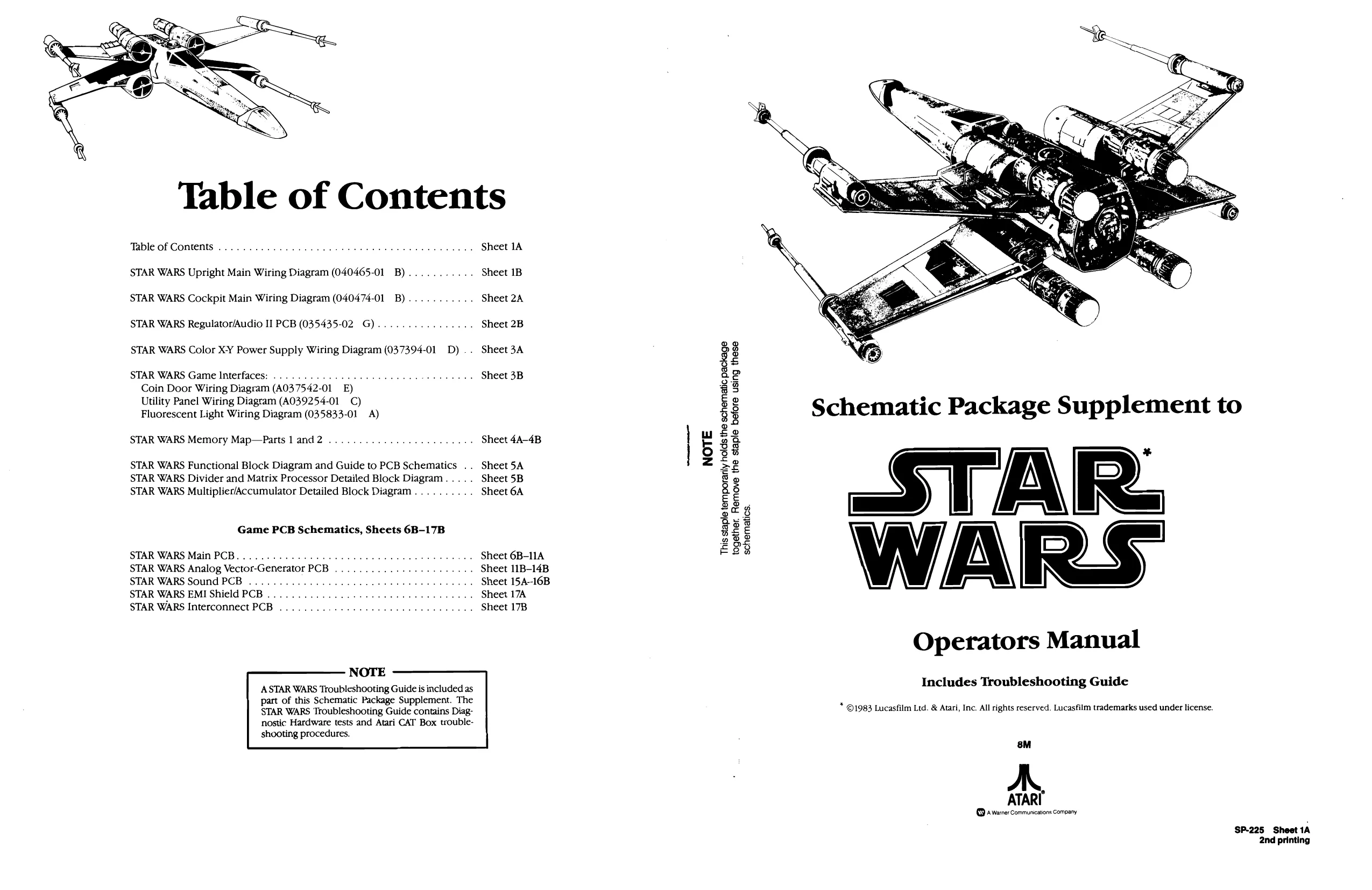
Table of Contents
Table of Contents .... 2... 666s Sheet 1A
STAR WARS Upright Main Wiring Diagram (040465-01 B)........... Sheet 1B
STAR WARS Cockpit Main Wiring Diagram (040474-01 B)........... Sheet 2A
STAR WARS Regulator/Audio II PCB (035435-02 G)............... Sheet 2B
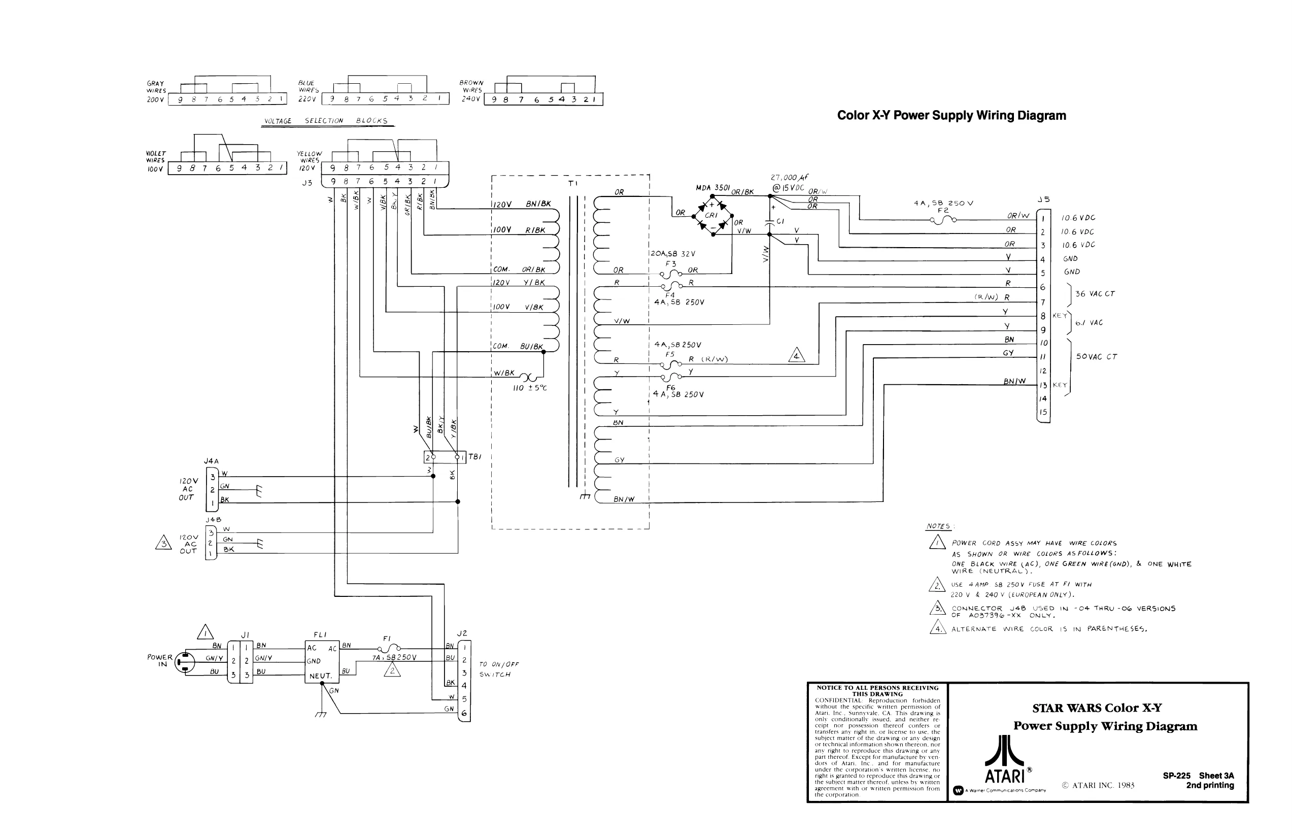
STAR WARS Color X-Y Power Supply Wiring Diagram (037394-01 D).. Sheet 3A
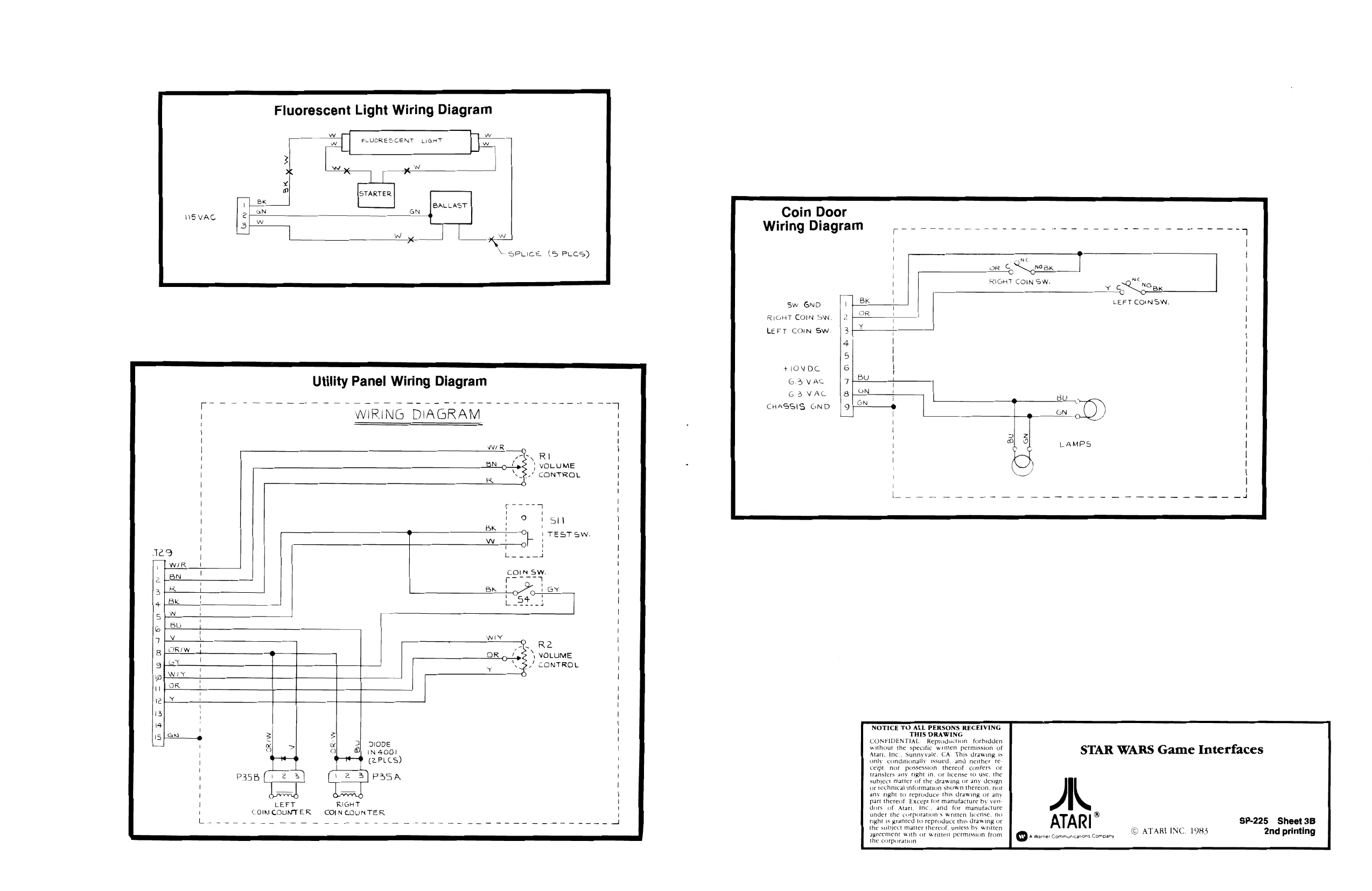
STAR WARS Game Interfaces: .....--. 6.60.0 eee eee Pen ens gene Sheet 3B Coin Door Wiring Diagram (A037542-01 E) Utility Panel Wiring Diagram (A039254-01 C) Fluorescent Light Wiring Diagram (035833-01 A) Schematic Package Supplement to
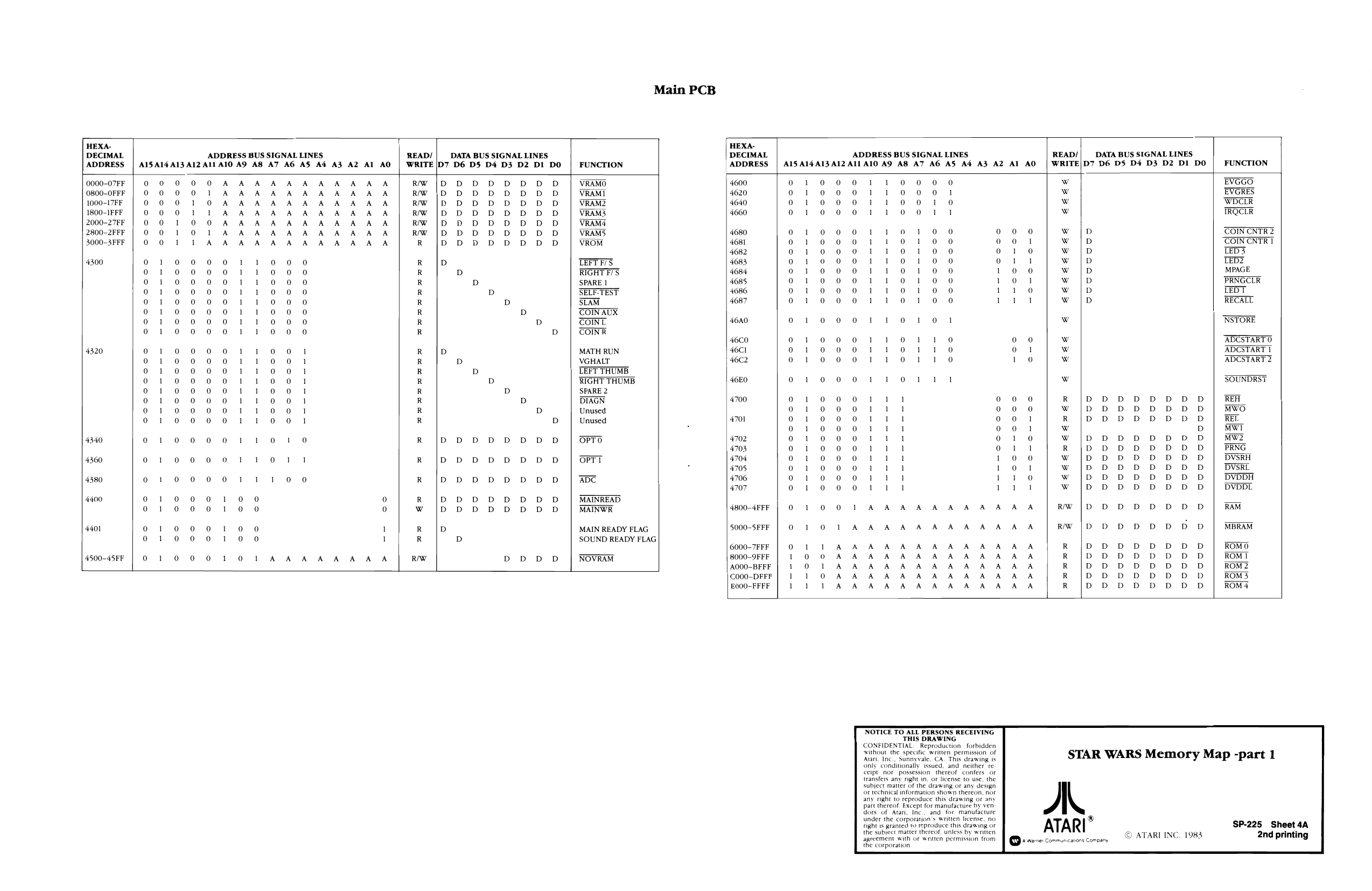
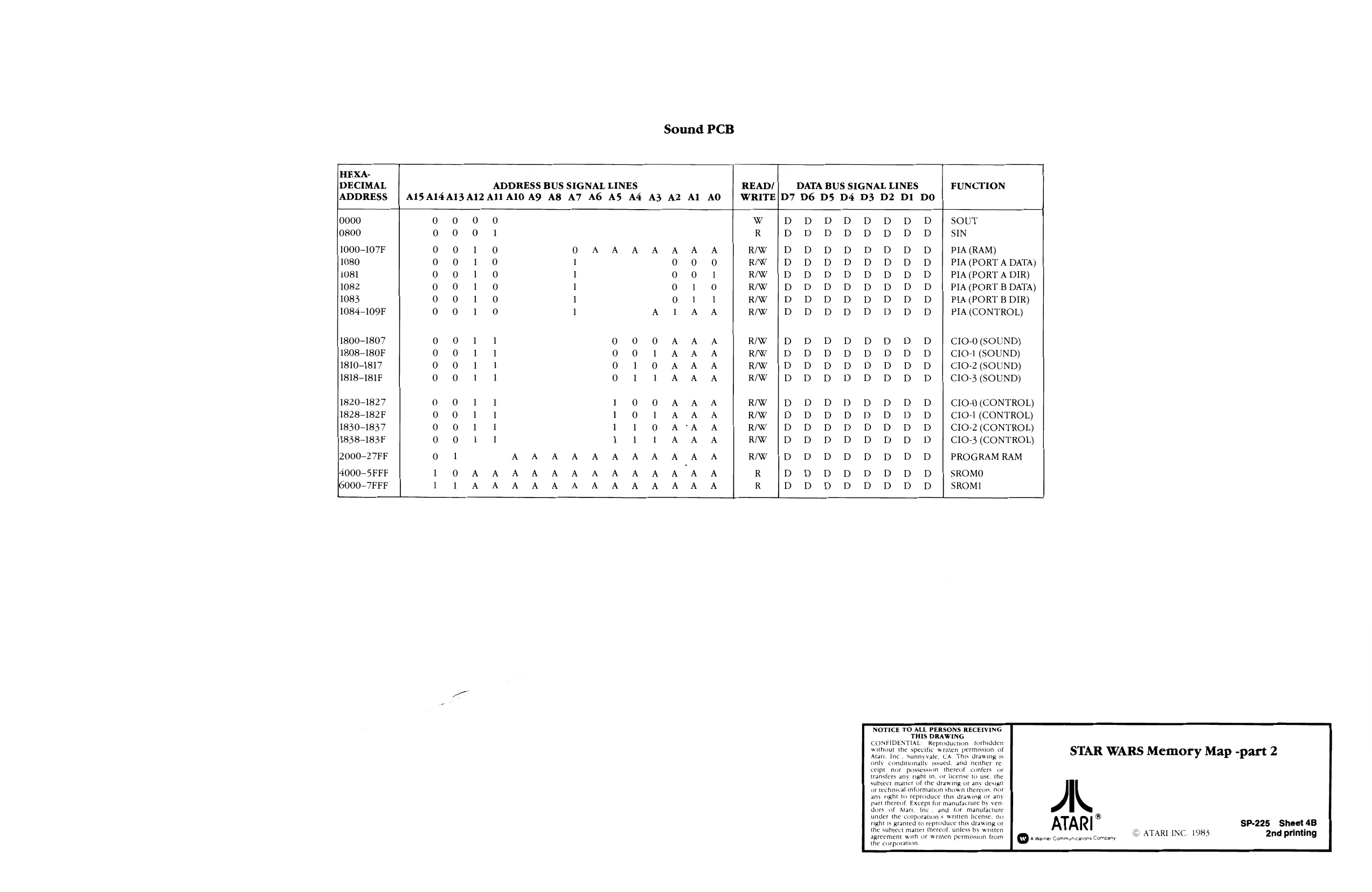
STAR WARS Memory Map—Parts 1 and2 ..... maw set gemmens pees Sheet 4A-4B * STAR WARS Functional Block Diagram and Guide to PCB Schematics .. Sheet 5A STAR WARS Divider and Matrix Processor Detailed Block Diagram... . . Sheet 5B STAR WARS Multiplier/Accumulator Detailed Block Diagram.......... Sheet 6A together. Remove the staple before using these
schematics. Game PCB Schematics, Sheets 6B-17B
STAR WARS Main PCB.........-.--...005. veeeeesees. Sheet 6B-11A STAR WARS Analog Vector-Generator PCB .............--- .. Sheet 11B-14B STAR WARS Sound PCB ...... Seve eee ee eee .. Sheet 15A-16B STAR WARS EMI Shield PCB . . . Sheet 17A STAR WARS Interconnect PCB ........ . Sheet 17B
Operators Manual
ASTAR WARS Troubleshooting Guide is included as Includes Troubleshooting Guide part of this Schematic Package Supplement. The STAR WARS Troubleshooting Guide contains Diag- * ©1983 Lucasfilm Ltd. & Atari, Inc. All rights reserved. Lucasfilm trademarks used under license. nostic Hardware tests and Atari CAT Box troubleshooting procedures. 8M
‘A Warner Communicatons Company SP.225 Sheet 1A 2nd printing
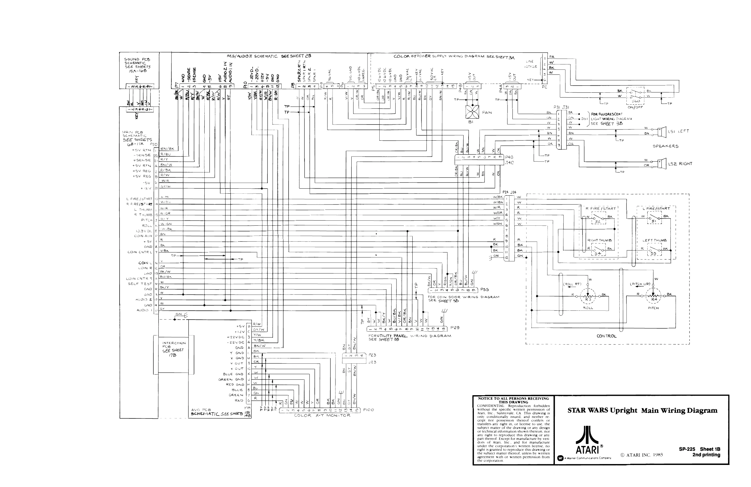
This page is a drawing, shown as the original scan.
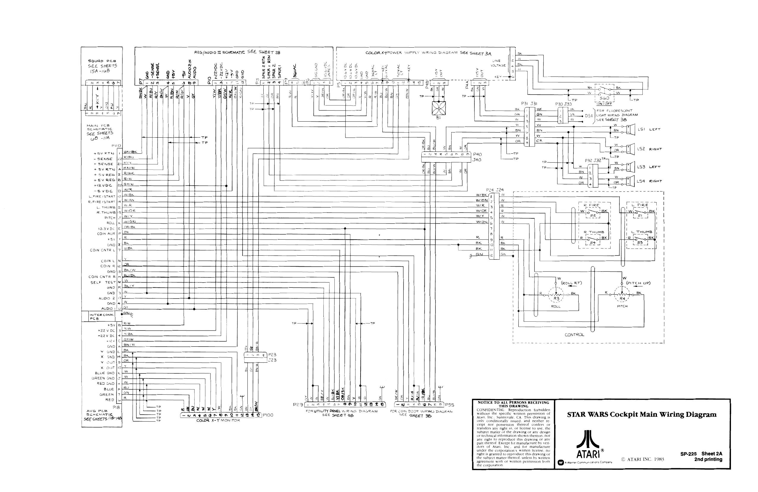
This page is a drawing, shown as the original scan.
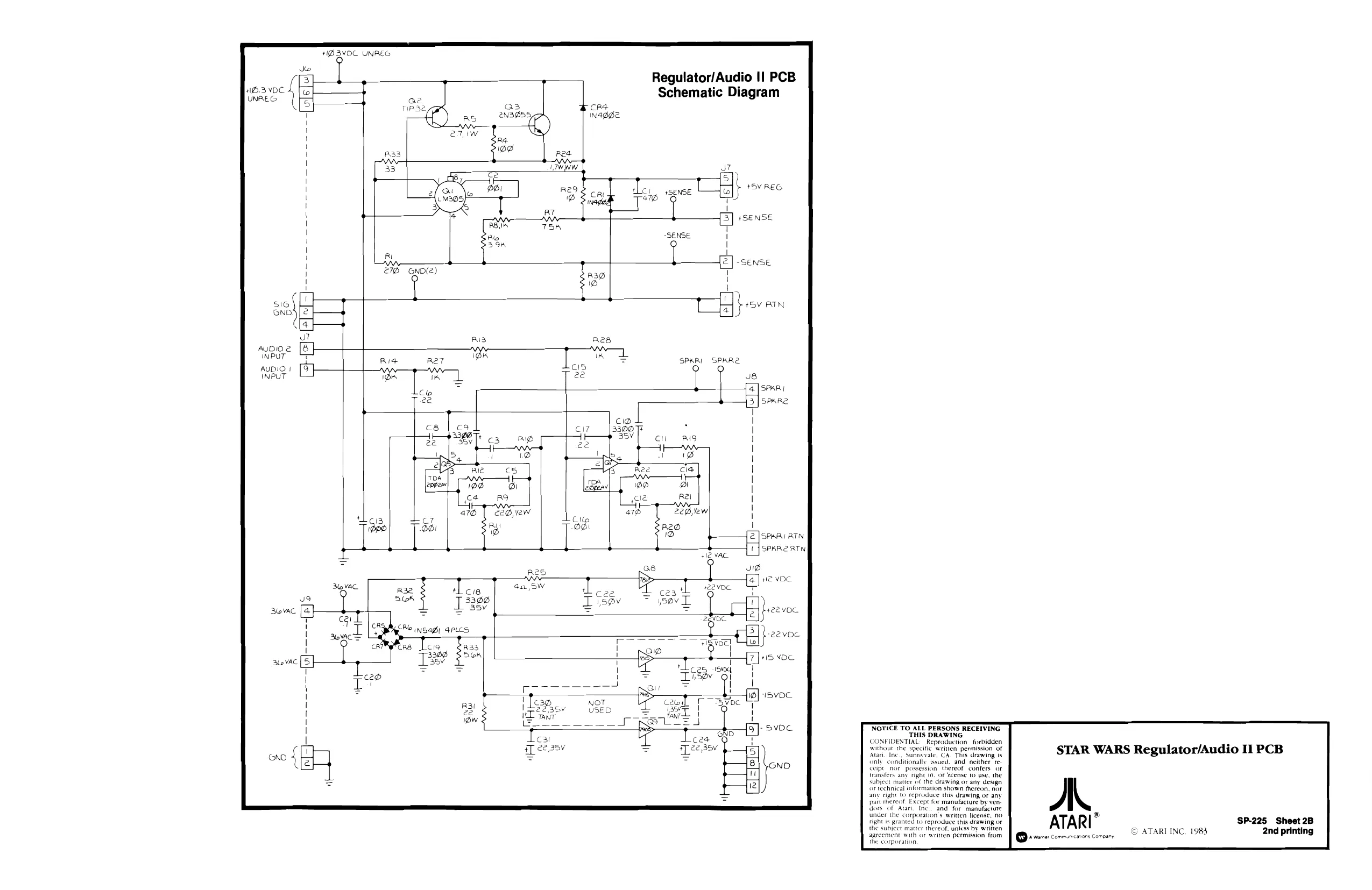
This page is a drawing, shown as the original scan.
This page is a drawing, shown as the original scan.
This page is a drawing, shown as the original scan.
This page is a drawing, shown as the original scan.
This page is a drawing, shown as the original scan.
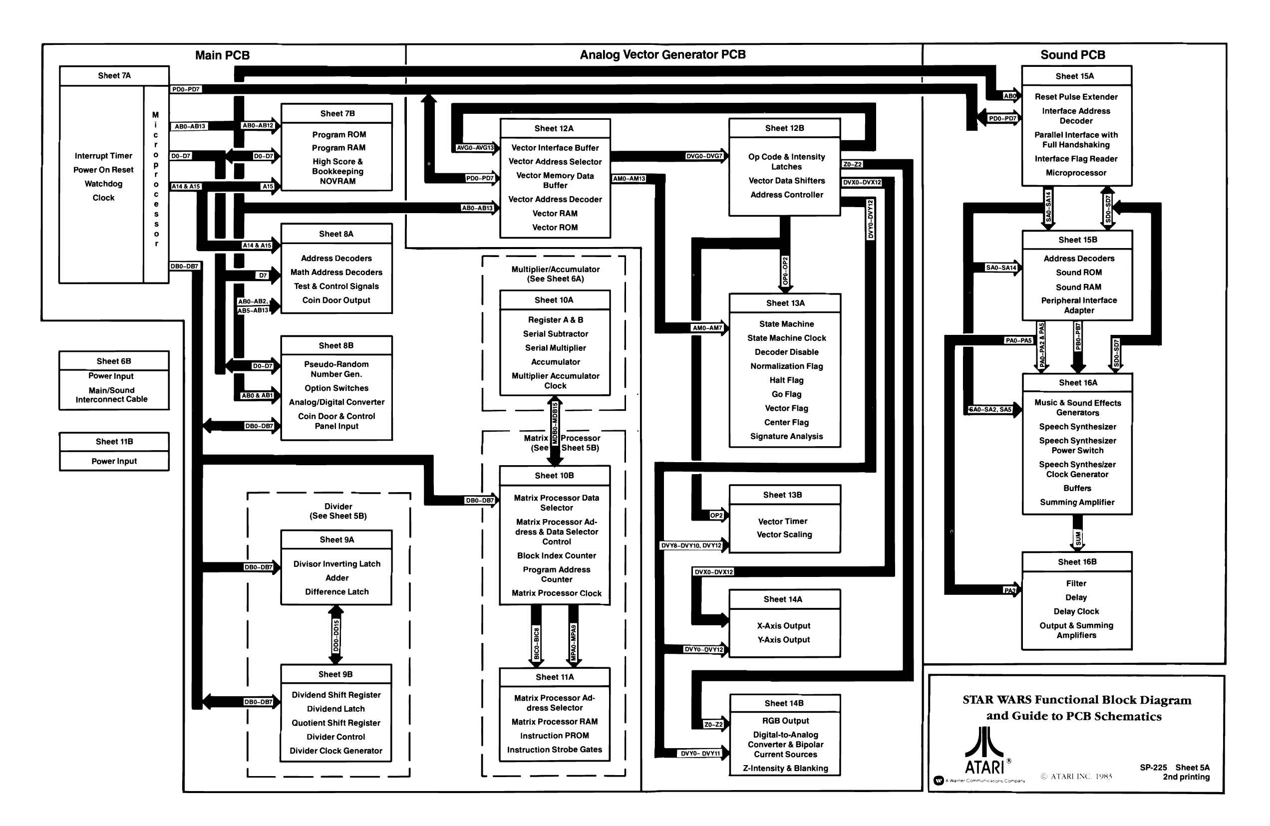
Main PCB Analog Vector Generator PCB Sound PCB
PDO-PD7, [Aso} Reset Pulse Extender Interface Address
Sheet 7B Decoder
| Sheet28 12B
Op Code & Intensity
Latches
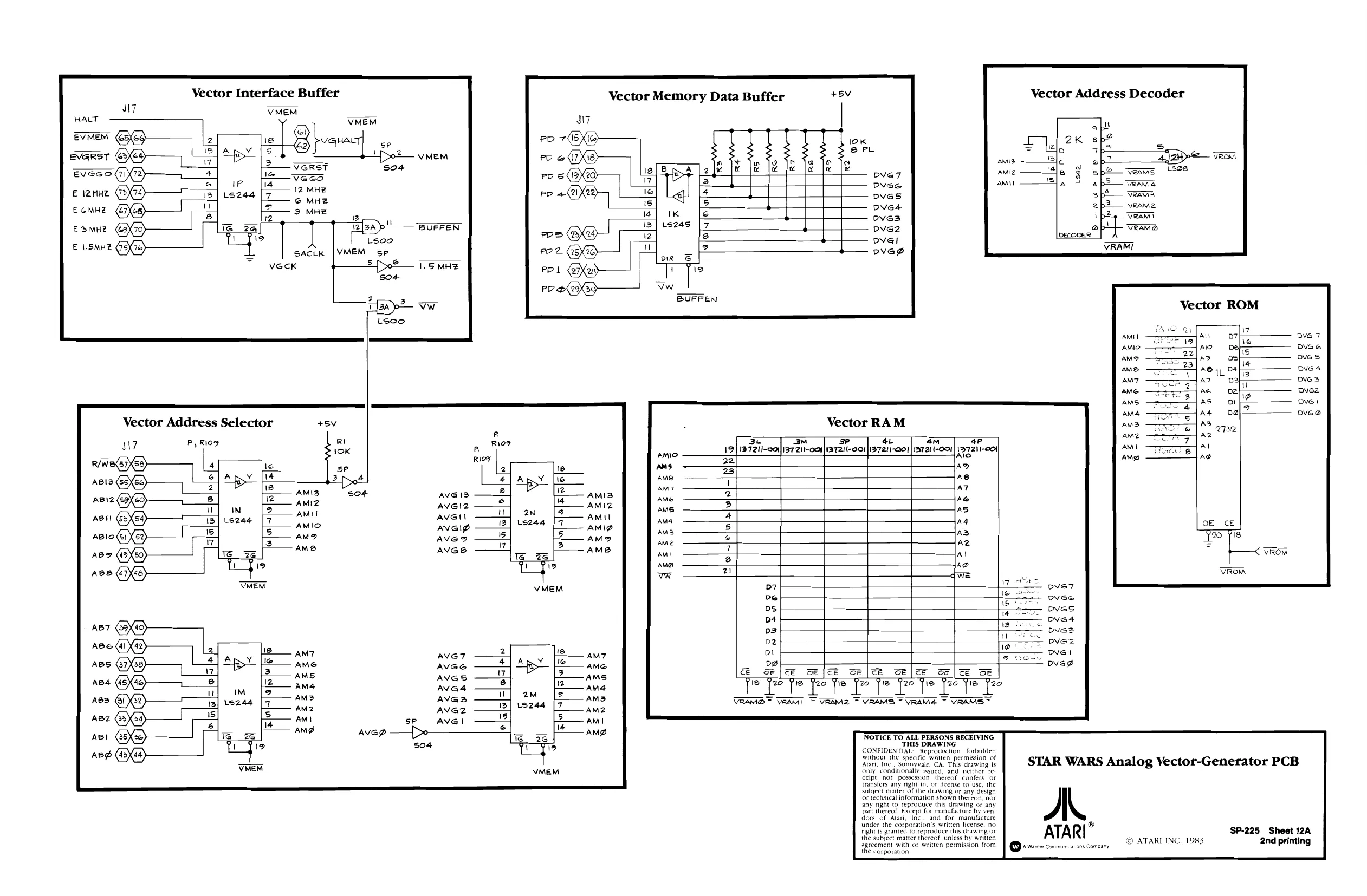
Vector Data Shifters Parallel Interface with Program ROM Program RAM [AVGO-AVG13} Vector Interface Buffer High Score & 7 Vector Address Selector Bookkeeping NOVRAM Full Handshaking Interface Flag Reader Microprocessor Interrupt Timer Power On Reset
Watchdog Clock ppo-pDy] «Vector Memory Data Buffer
Vector Address Decoder
Vector RAM
Vector ROM Address Controller
ABO-ABIS. rOnHveroATDONOE Ara & ANS) Address Decoders Address Decoders Math A D Multiplier/Accumulator ROM
| \ddress | Decoders | paaennrn | Sound | RO! |
Test & Control Signals Sound RAM
[ABO-AB2, Coin Door Output Peripheral Interface
(B5-AB13! Adapter Register A&B State Machine Seca a ail State Machine Clock
eet Serial Multiplier Decoder Disable Pseudo-Random Accumulator Normalization Flag
| Fowar input | Number Gen. | Multiplier Accumulator | Halt Flag |
Main/Sound Option Switches Go Fiag Interconnect Cable Analog/Digital Converter Vector Flag Music & Sound Effects Coin Door & Control éonterki Generators
| Panel Input | enter | Flag | Speech Synthesizer |
(See fa Sheet 5B) Power Switch
Speech Synthesizer Clock Generator
Buffers | Sheet 10B 1 D50-DE Matrix Processor Data ‘ _
Divider Selector Summing Amplifier
(See Sheet
| (See Sheet SB) | Matrix Processor Ad- | Vector Timer |
dress & Data Selector Vector Scaling 6 Control
Block Index Counter Sheet ee i i h Divisor Inverting Late! Program Address Adder
Difference Latch Counter Filter Delay Delay Clock Output & Summing ‘Amplifiers X-Axis Output ¥-Axis Output ‘DD0-DD16) | Matrix Processor Clock |
Dividend Shift Register Dividend Latch
Quotient Shift Register STAR WARS Functional Block Diagram and Guide to PCB Schematics A ATARI® SP-225 Sheet 5A © iwi communcanonscomoary © ATARTING. 1983 2nd printing dress Selector
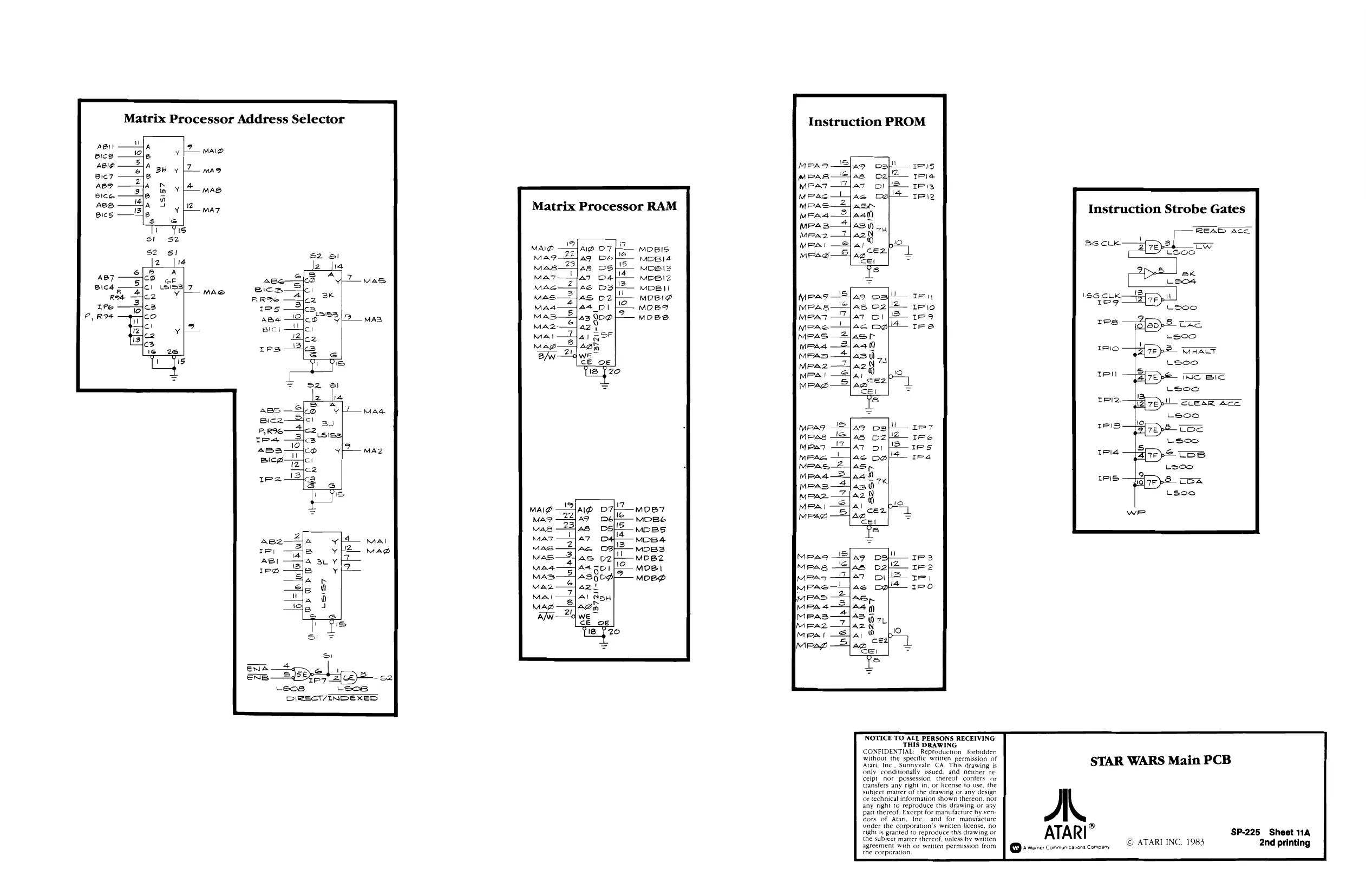
Matrix Processor RAM
Instruction PROM
Instruction Strobe Gates RGB Output Digital-to-Analog Converter & Bipolar Current Sources Divider Control
Divider Clock Generator DVYO- DVYIT | Matrix Processor Ad-
Z-Intensity & Blanking a |
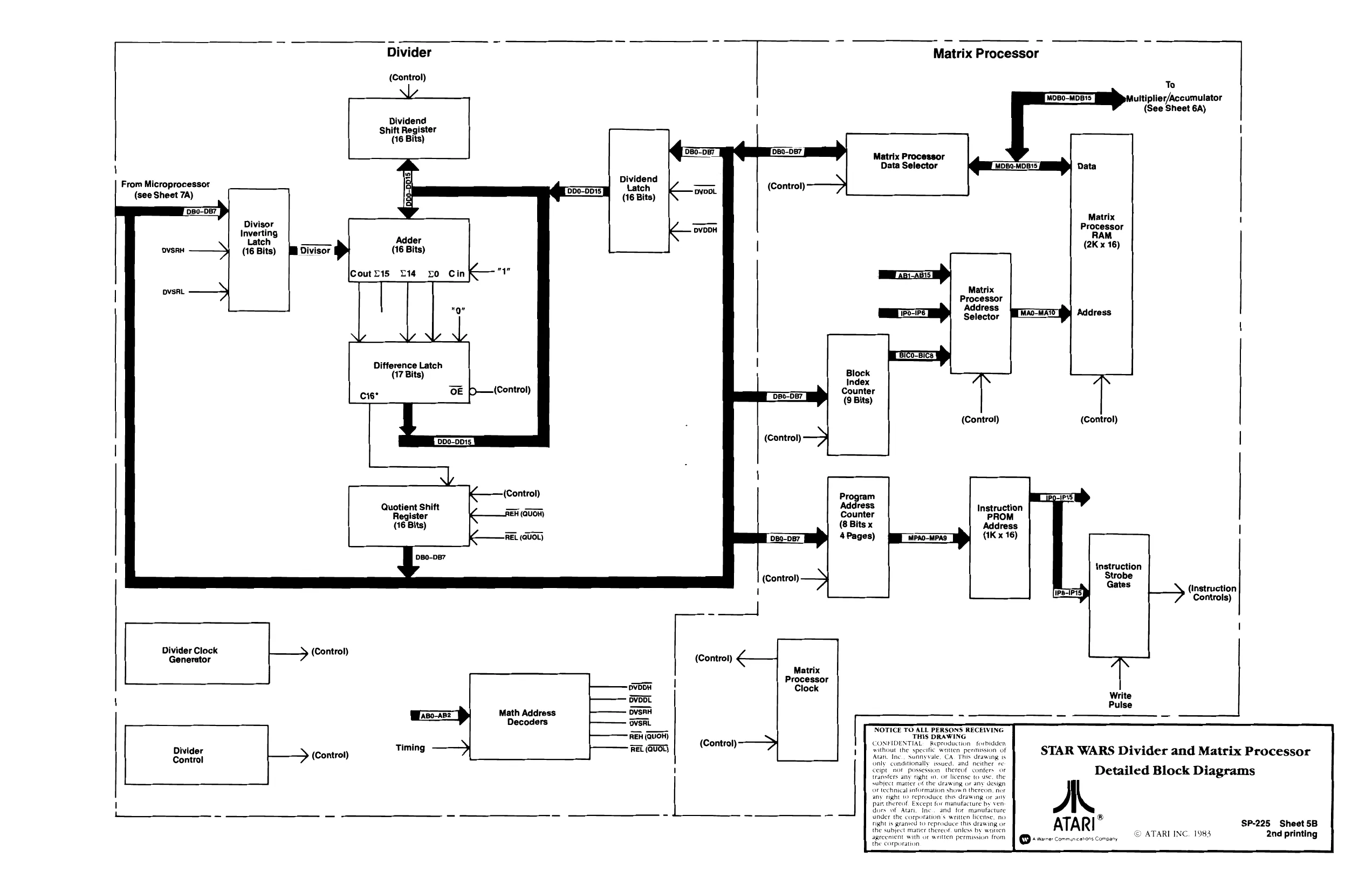
From Microprocessor (see Sheet 7A)
Divisor Inverting Latch ernst
‘OVSRH (16 Bits) Divisor
DVvSRL
Divider Clock Generator
Divider Control (Control)
(Control) ider
(Control)
Dividend Shift Register (16 Bits)
Dividend ‘DD0-DD15)
(16 Bits)
[CoutLi5 £14 xo Cin
Difference Latch l (17 Bits)
cis"
\
Quotient Shift Register (16 Bits)
\
(Control)
Math Address Decoders
Timing [DB0-087,
(Control)
DB0-DB7
(Control) To ultiplier/Accumulator (See Sheet 6A)
I
Matrix Processor
Data Selector Data
Matrix 1
Processor RAM (2K x 16)
Matrix Leip ress Selector PLMAI-MAIOy Address
[5Ico-Bicey
Block Index Counter (9 Bits)
Program Address Counter (8 Bits x 4 Pages)
CONFIDENTIAL
Aun. Inc
Ade (Control)
Instruction PROM
{1K x 16) (Control)
dress
instruction Strobe
Gates (instruction
Controls)
'
Write Pulse
= =
NOTICE TO ALL PERSONS RECEIVE THIS DRAWING. Reproduction forbidden 1 J without the specttic watten permission of sunnyvale, CA This drawing is only’ conditionally issued. and. neither +e ceipt nor possession thereof confers or transfers any right an. or license to use, the ING
STAR WARS Divider and Matrix Processor
Detailed Block Diagrams
subject matter of the drawing or any design Or technical information shown thereon, nvr any night to reproduce this drawing or any part thereat. Except for manufacture by ven: dors Of tan, Inc under the corporation's written license, no right is granted to reproduce this drawing or the subject ma agreenient with or weitten permission from and. for manutac
thereof. unless by wei
the corporation SP-225 Sheet 5B 2nd printing ATARI* © +26: communcarons Comoany © ATARI INC. 1983
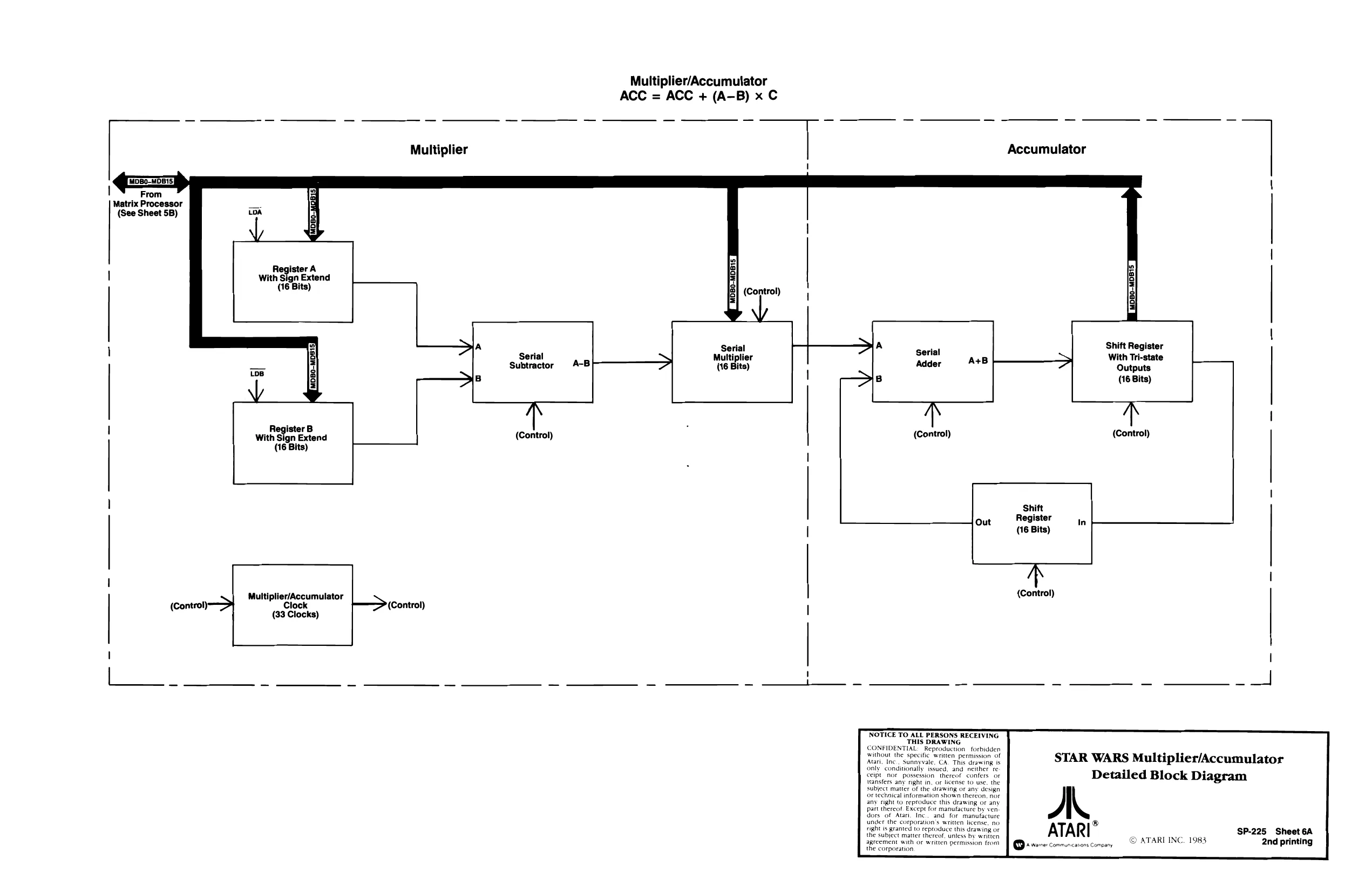
This page is a drawing, shown as the original scan.
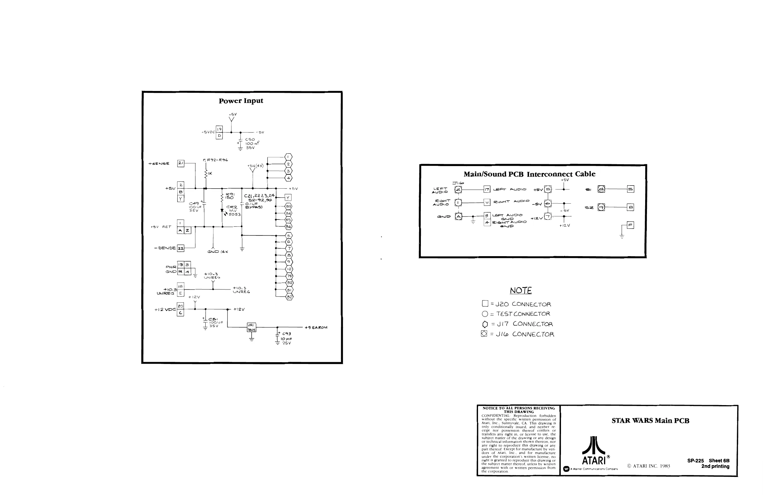
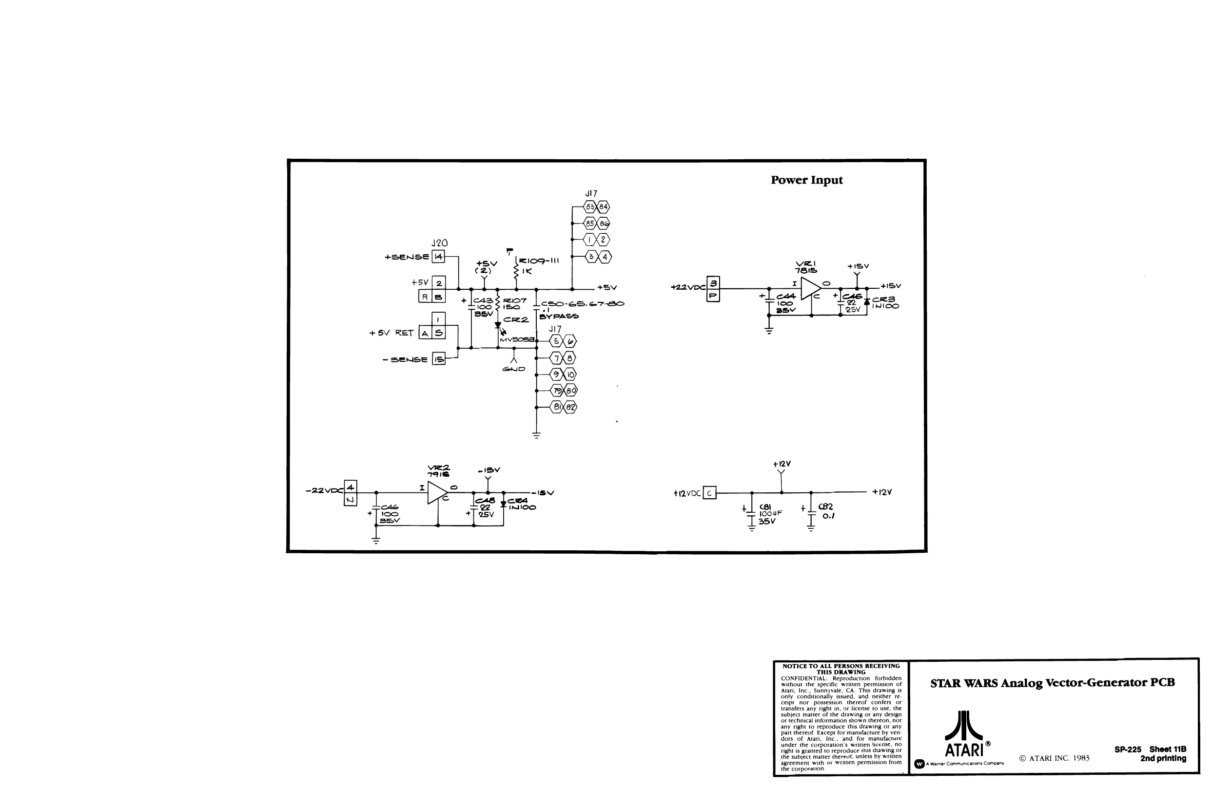
Power Input
T -sv
+sul4d)
as ey rod Jessel a
=
+5 EAROM Main/Sound PCB Interconnect Cable +5V die
weer Auvio sv ([S)
RiatT AUSIS -Ev =}—- -5v Leet AUDIO navO)}——euD RieHT Aus pals ri2V
NOTE
CJ =u2o0 CONNECTOR
O = TEST CONNECTOR
OQ =JI7 CONNECTOR
© = Ul& CONNECTOR
NOTICE TO ALL PERSONS RECEIVING THIS DRAWING CONFIDENTIAL: Reproduction forbidden without the specific weitten permission of Atari, Inc., Sunnyvale, CA. This drawing IS only conditionally issued, and neither re ceipt nor possession thereof confers or transfers any right in, of license to use. the subject matter of the drawing or any design
or technical information shown thereon, not
any right (© reproduce this drawing of any part thereof Except for manufacture by ven dors of Atari, Inc. and. for manufacture under the corporation's written license, no right ts granted to reproduce this drawing oF the subject matter thereof, unless by written = &
sz ©
A
ATARI*
secon " Owns : STAR WARS Main PCB
SP-225 Sheet 6B © ATARI INC. 1983 2nd printing
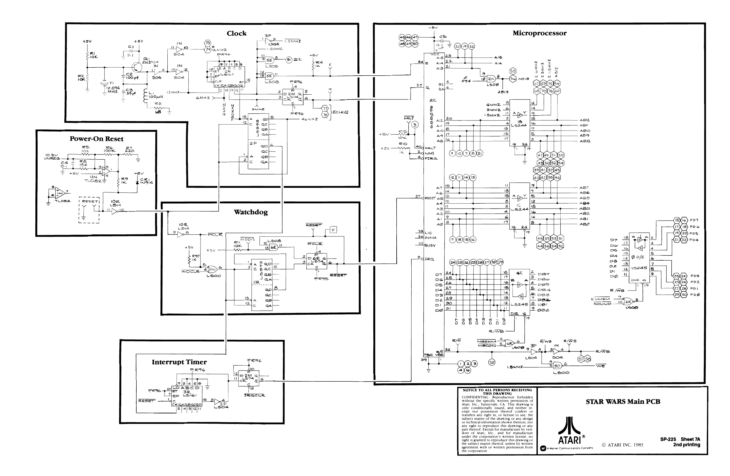
This page is a drawing, shown as the original scan.
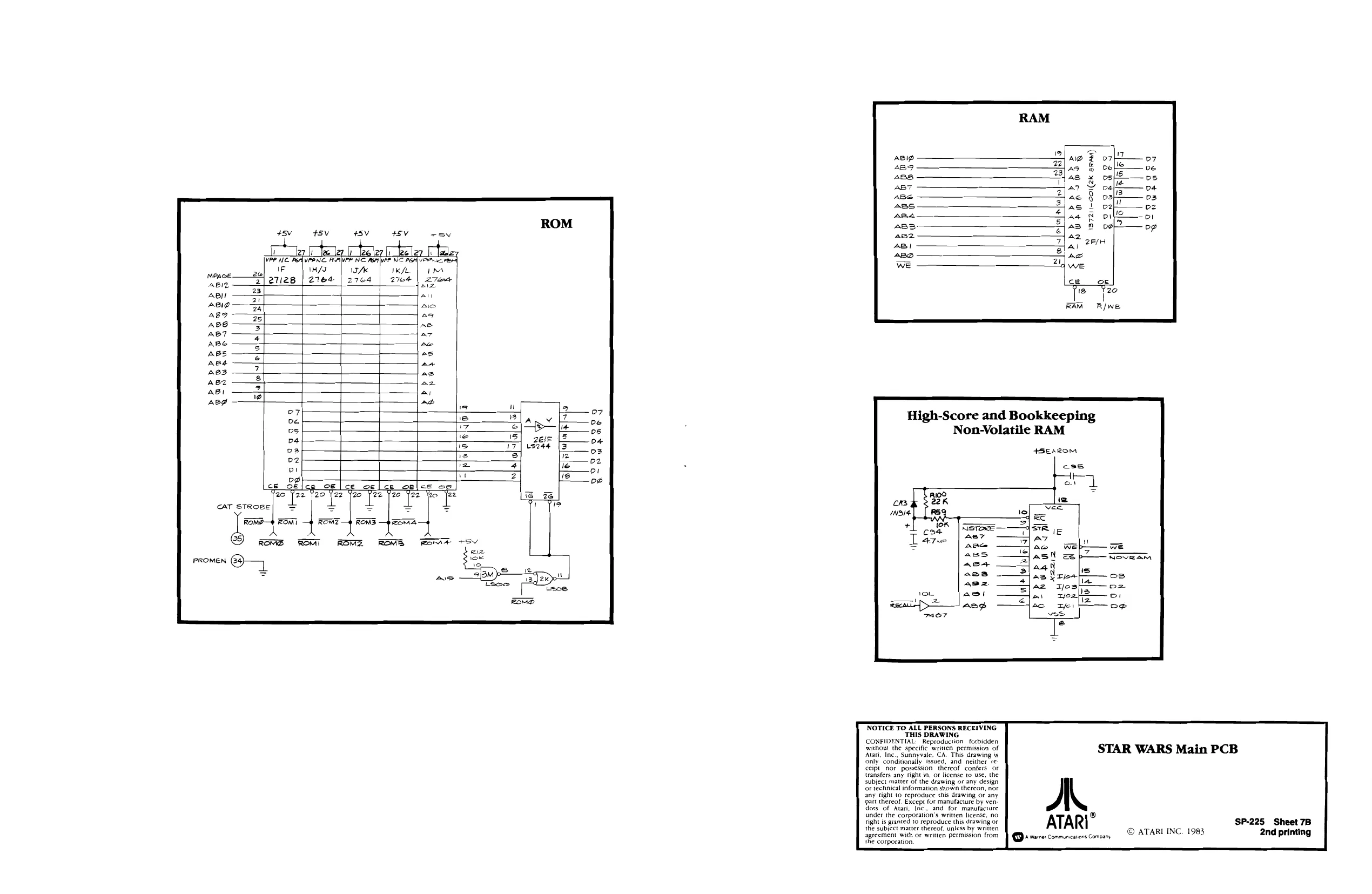
This page is a drawing, shown as the original scan.
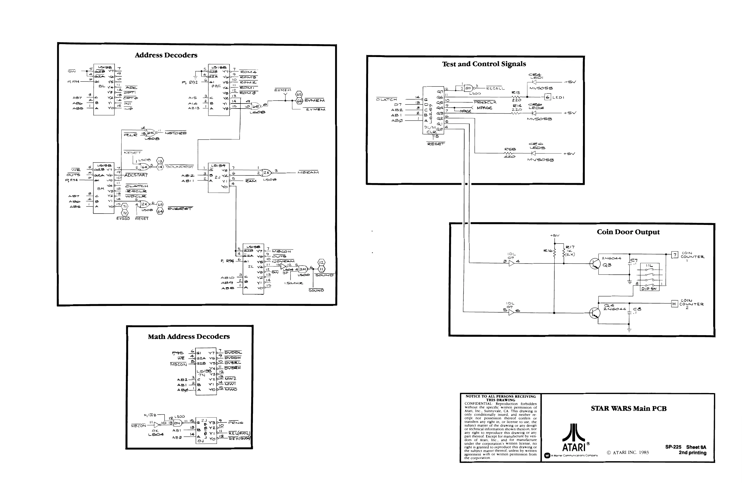
This page is a drawing, shown as the original scan.
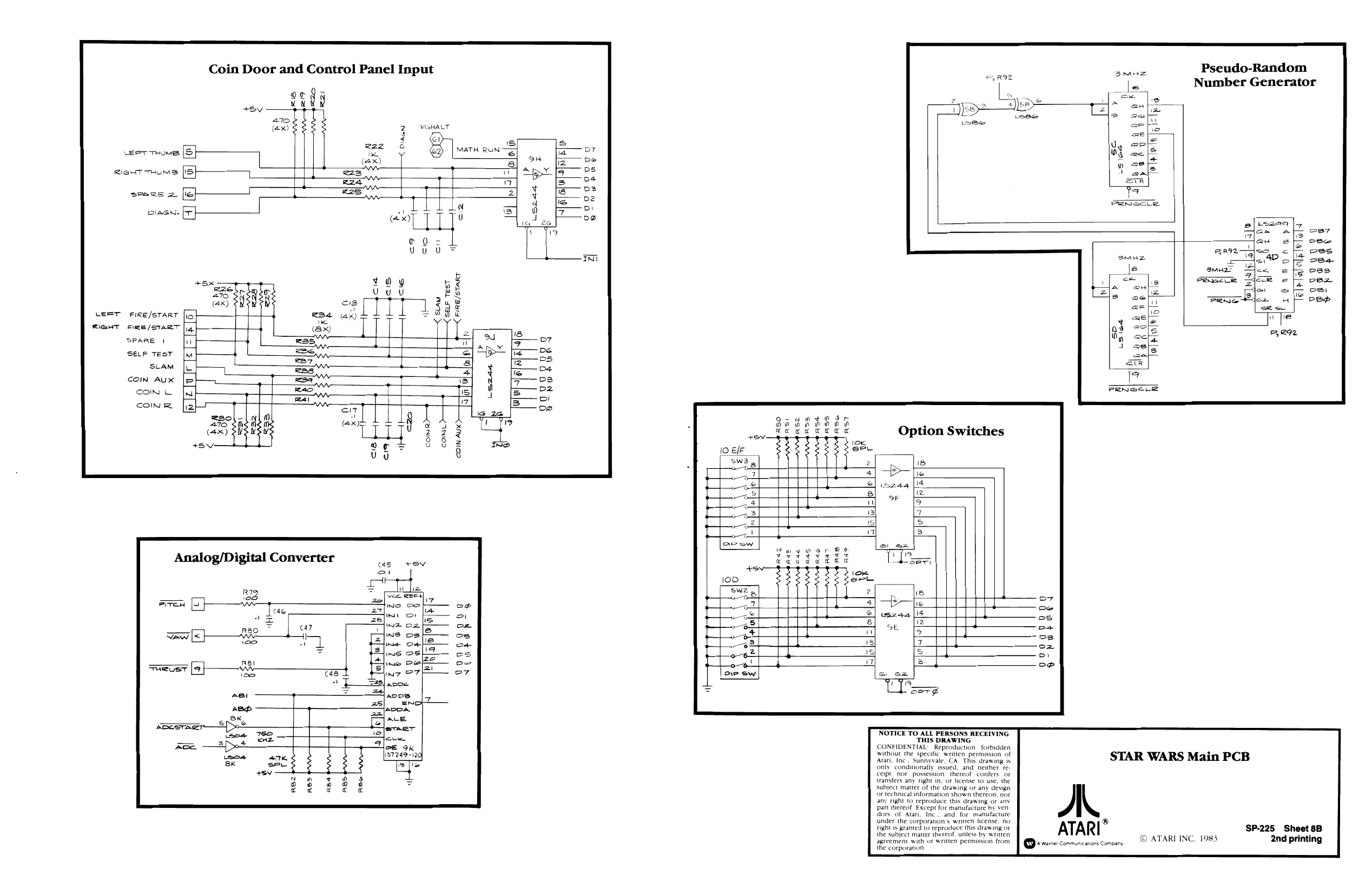
Coin Door and Control Panel Input
cdg u
(40
LEST Fige/sTART RieuT cme /StAeT SPARE |
SELF TesT
SLAM
COIN AUX
CON LL
COIN MATH RUN ‘S|
Analog/Digital Converter
SB Tea "= R80 ca? eS ; 1
a8
ASDA, ALE
jeracr
OE 9K 37249 -12 R92
PW Igelpe
Pseudo-Random Number Generator
> = [Rio
Tolelals 151
NOTICE TO ALL PERSONS RECEIVING THIS DRAWING CONFIDENTIAL: Reproduction forbidden without the specific written permission of Inc., Sunnyvale, CA. This drawing is conditionally issued, and neither te- Ceipt_nor possession thereof confers or transfers any right in, or license to use, the subject matter of the drawing or any design
for technical information shown thereon, not
any right to reproduce this drawing or any part thereof. Except for manufacture by ven dors of Atari, Inc,, and for manufacture under the corporation's written license, no right 1s granted to reproduce this drawing or the subject matter thereof, unless by written agreement with of Weitten permission from the corporation.
STAR WARS Main PCB
A. ATARI” > 12106: Communications Company © ATARI INC. SP-225 Sheet 8B 1983 2nd printing
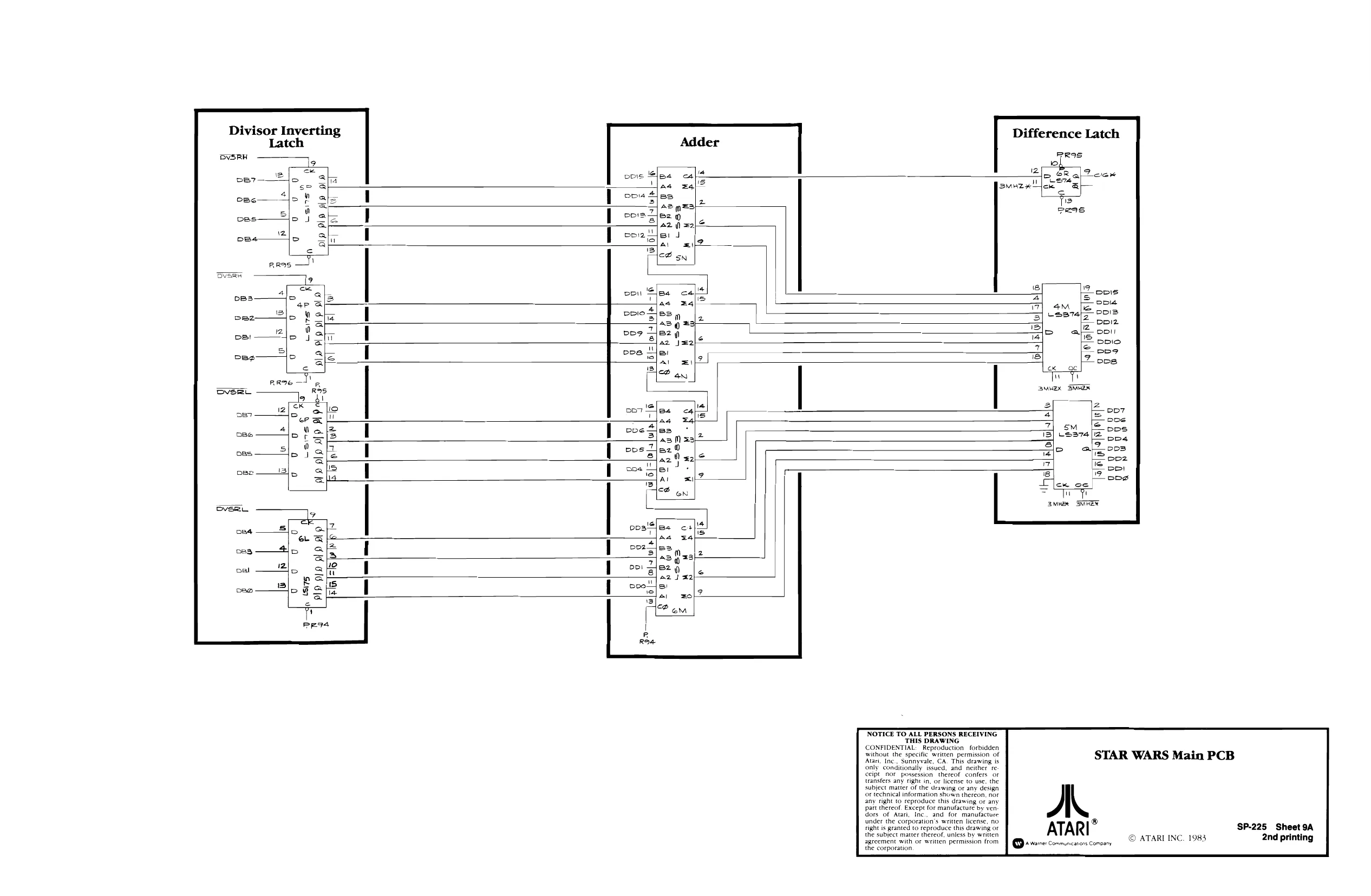
This page is a drawing, shown as the original scan.
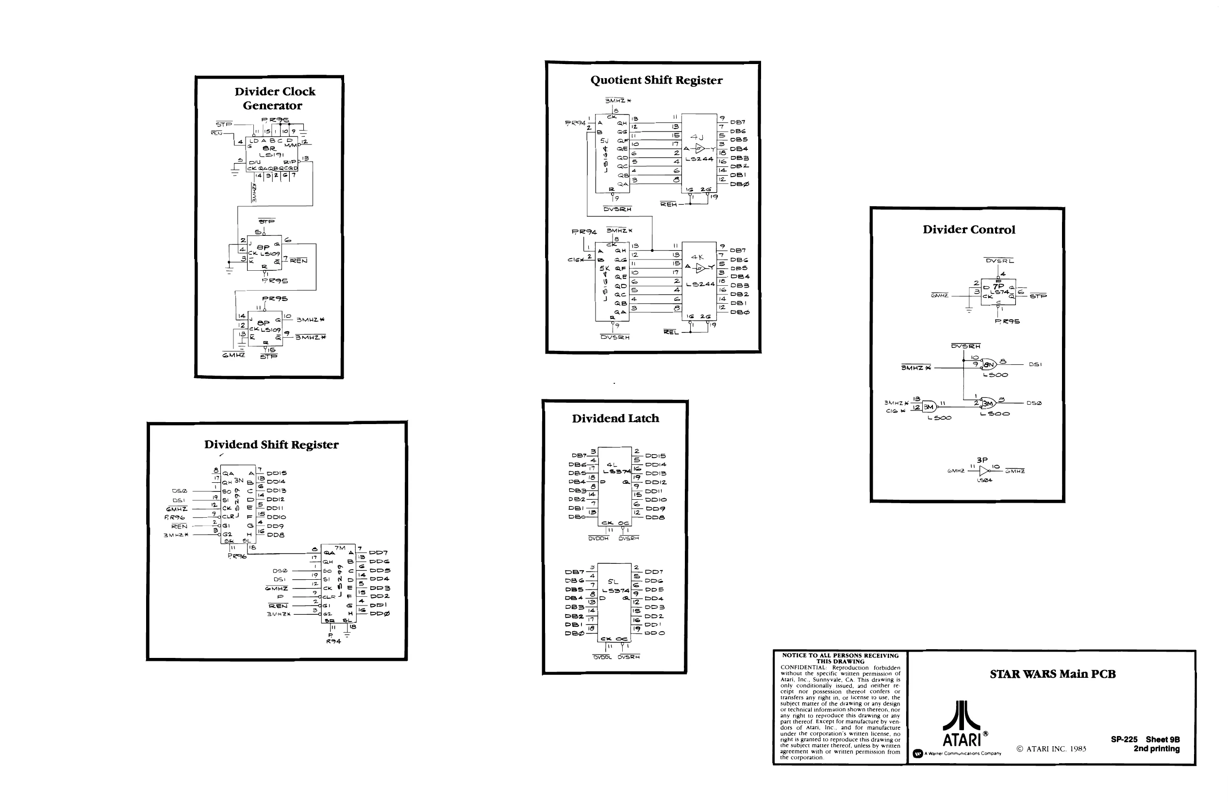
This page is a drawing, shown as the original scan.
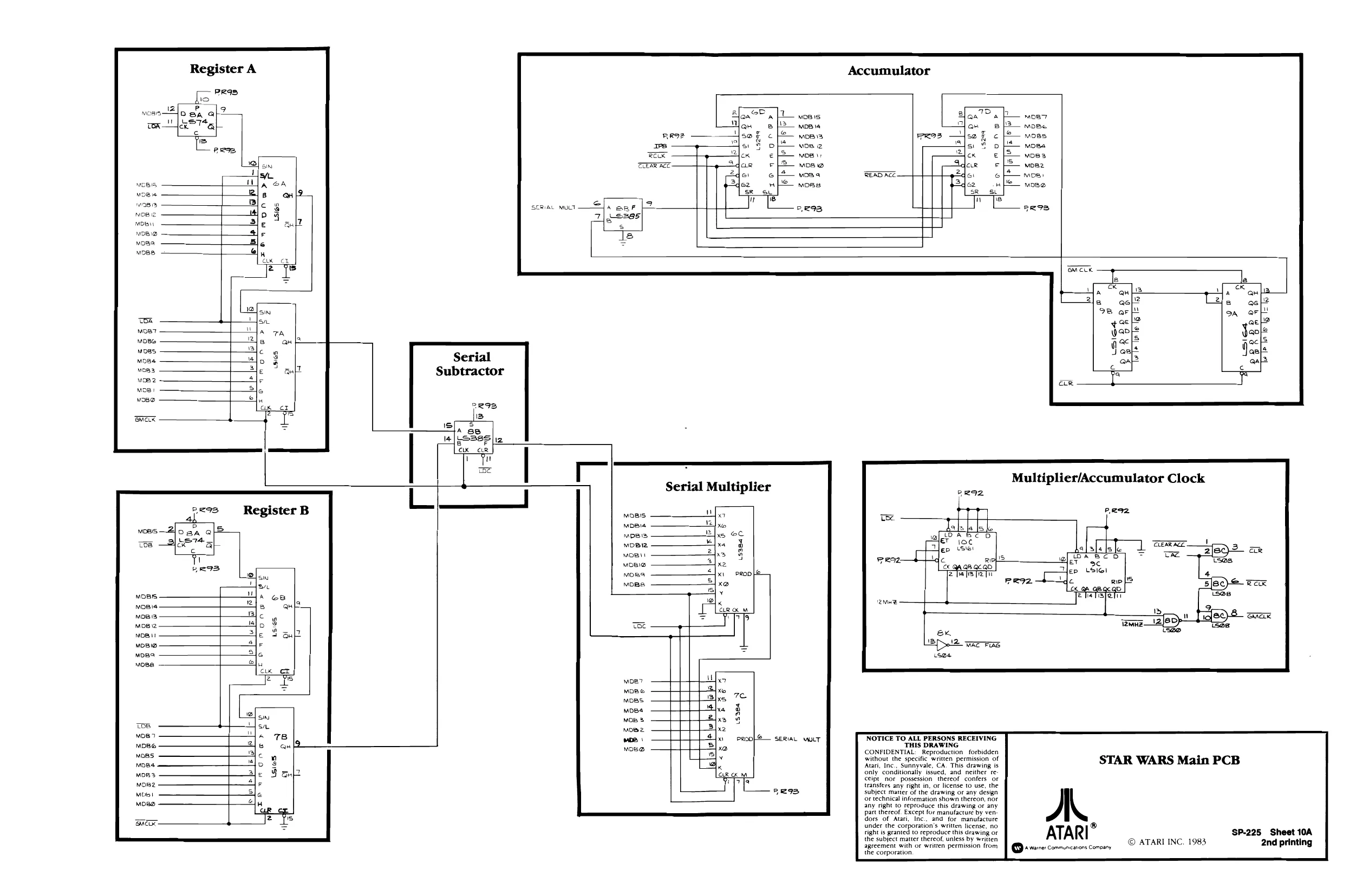
Register A
Serial Subtractor
2Rq lis s A 88 14 | S385 [12 cad r TERR REE. |4— vom
Le moss TOamonBy
@| ronmonge BERD ACE. a 3d.
Ck ce ou
mm
Ly o peo ™M Ono Lsies 9!
BR kd LW)
Serial Multiplier
e SERIAL WUT bri bh kb
Multiplier/Accumulator Clock
"NOTICE TO ALL PERSONS RECEIVING ‘THIS DRAWING CONFIDENTIAL: Reproduction forbidden without the specific written permission of Atari, Inc., Sunnyvale, CA. This drawing is only conditionally issued, and neither re ceipt_nor possession thereof confers or transfers any right in, or license to use, the subject matter of the drawing or any design Or technical information shown thereon, nor any right to reproduce this drawing or any part thereof. Except for manufacture by ven dors of Atari, Inc., and for manufacture under the corporation’s written license, no
right is granted to reproduce this drawing or
the subject matter thereof, unless by written agreement with or written permission from the corporation
STAR WARS Main PCB
A.
ATARI”
vee conmncatans Conny © ATARI INC. 1983 SP.225 Sheet 10A 2nd printing
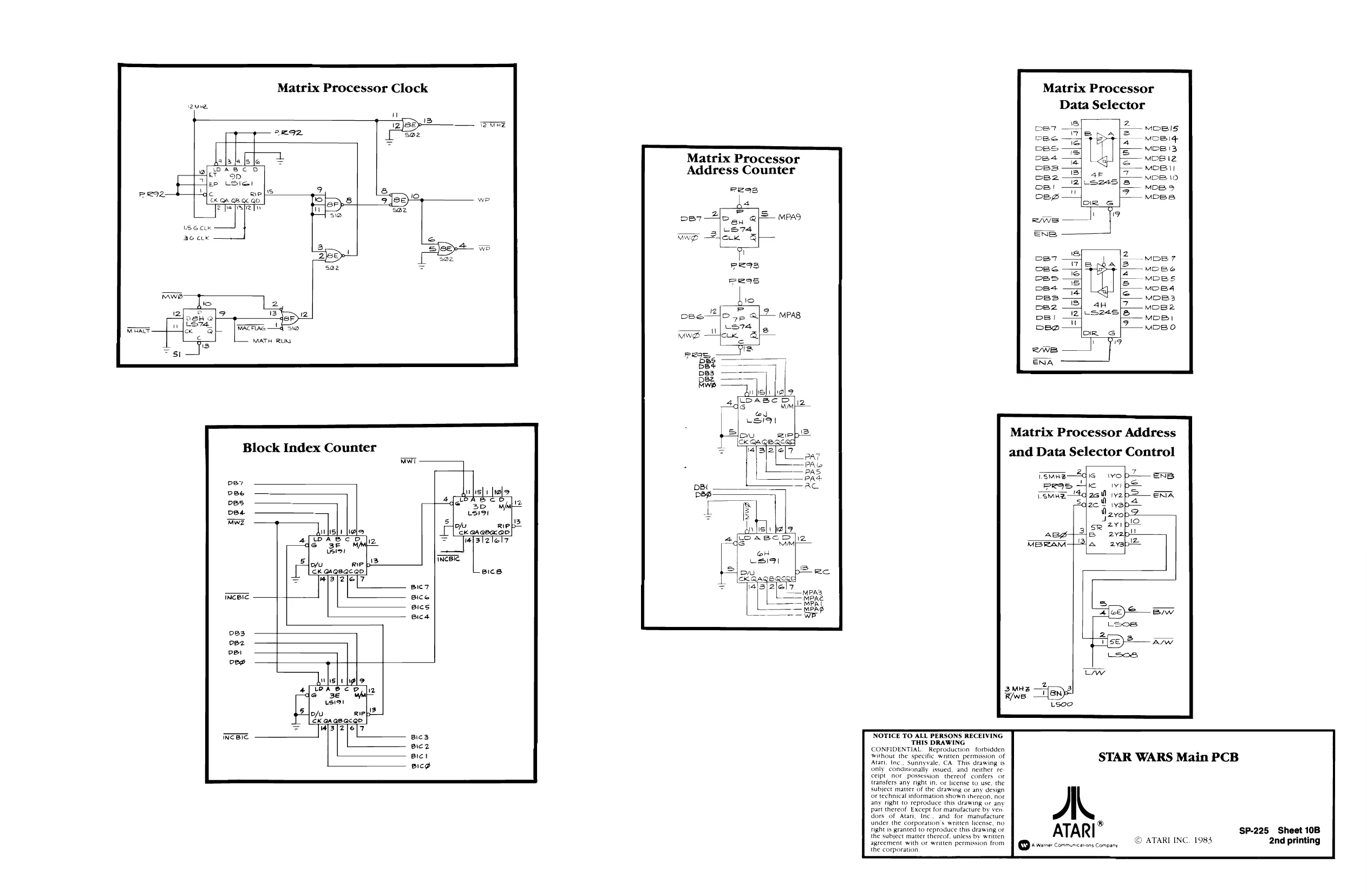
This page is a drawing, shown as the original scan.
This page is a drawing, shown as the original scan.
This page is a drawing, shown as the original scan.
This page is a drawing, shown as the original scan.
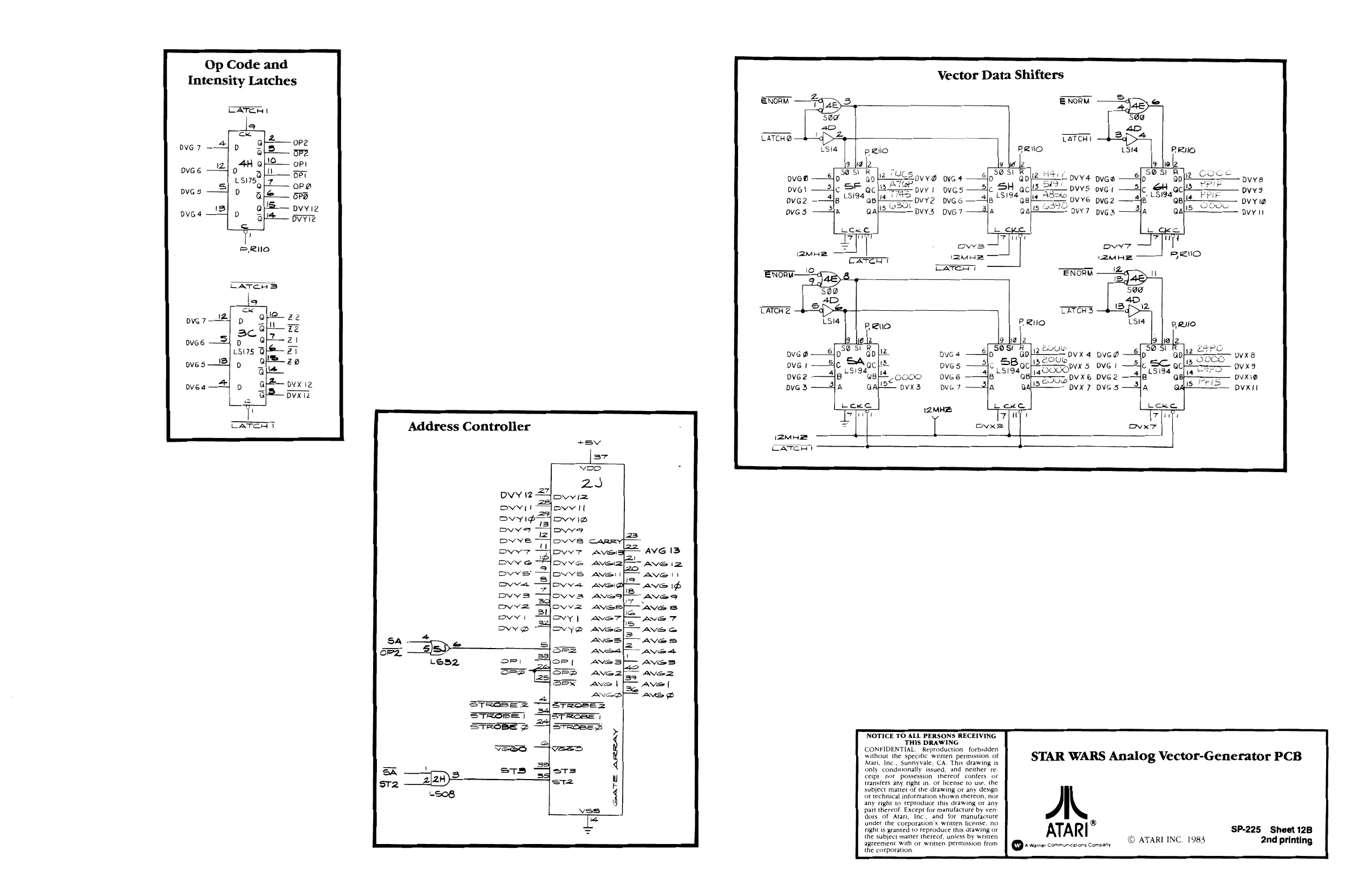
Op Code and
Intensity Latches
y SW? of O > dlo ole lo
Address Controller
Vector Data Shifters
12 TICS yy g 3 ATGP pi. THE ov! {4 ovr2 PRE CO0G Hs Dvy3
12 Boue vx BZOUGNNX 4 DVGO [aDOUPYX 5 OVE! pew OVXE DVGZ
I2MHe = DVX7 DVSS
CATTERY
NOTICE TO ALL PERSONS RECEIVING THIS DRAWING CONFIDENTIAL: Reproduction forbidden without the specific written permission of Aaari, Inc., Sunnyvale, CA. This drawing is only conditionally issued, and neither re ceipt pat possession thereof canfers or transfers any right in, oF license to use, the
subject matter of the drawing or any design
Or technical information shown thereo any right to reproduce this drawing part thereof. Except for manufacture by ven. dors of Atari, Inc., and for manufacture Under the corporation's written license, no right is granted to reproduce this drawing or the subject matter thereof, unless by written agreement with or written permission from the corporation
STAR WARS Analog Vector-Generator PCB
AL
ATARI®
© ATARI INC. ‘SP-225 Sheet 12B 1983 2nd printing
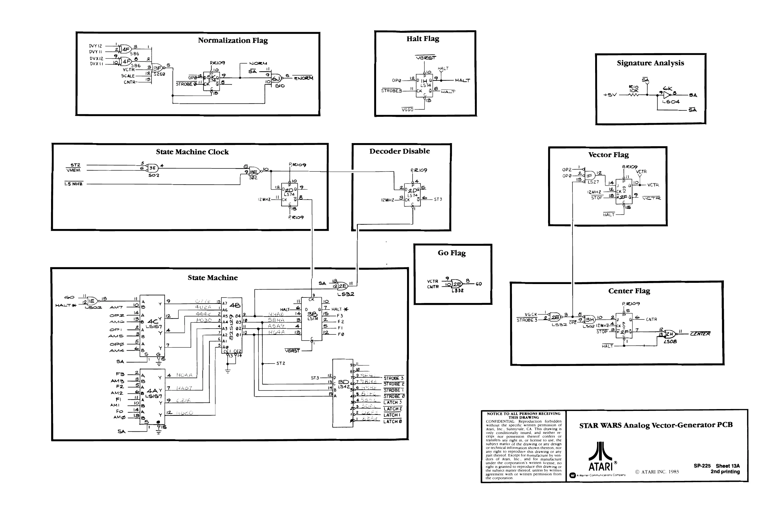
This page is a drawing, shown as the original scan.
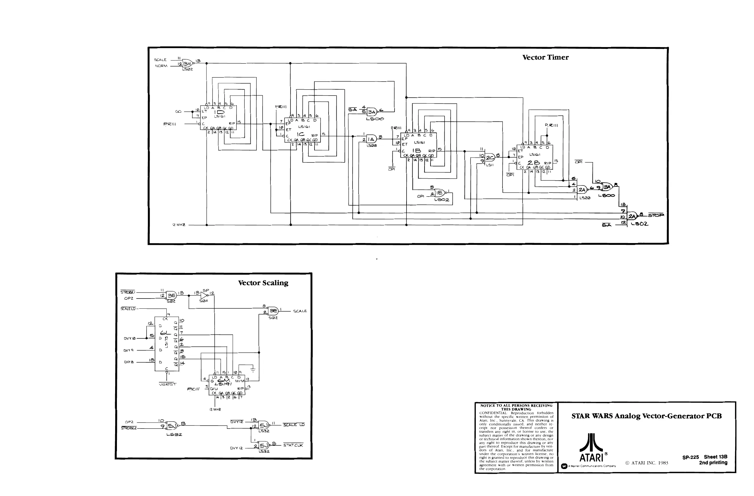
This page is a drawing, shown as the original scan.
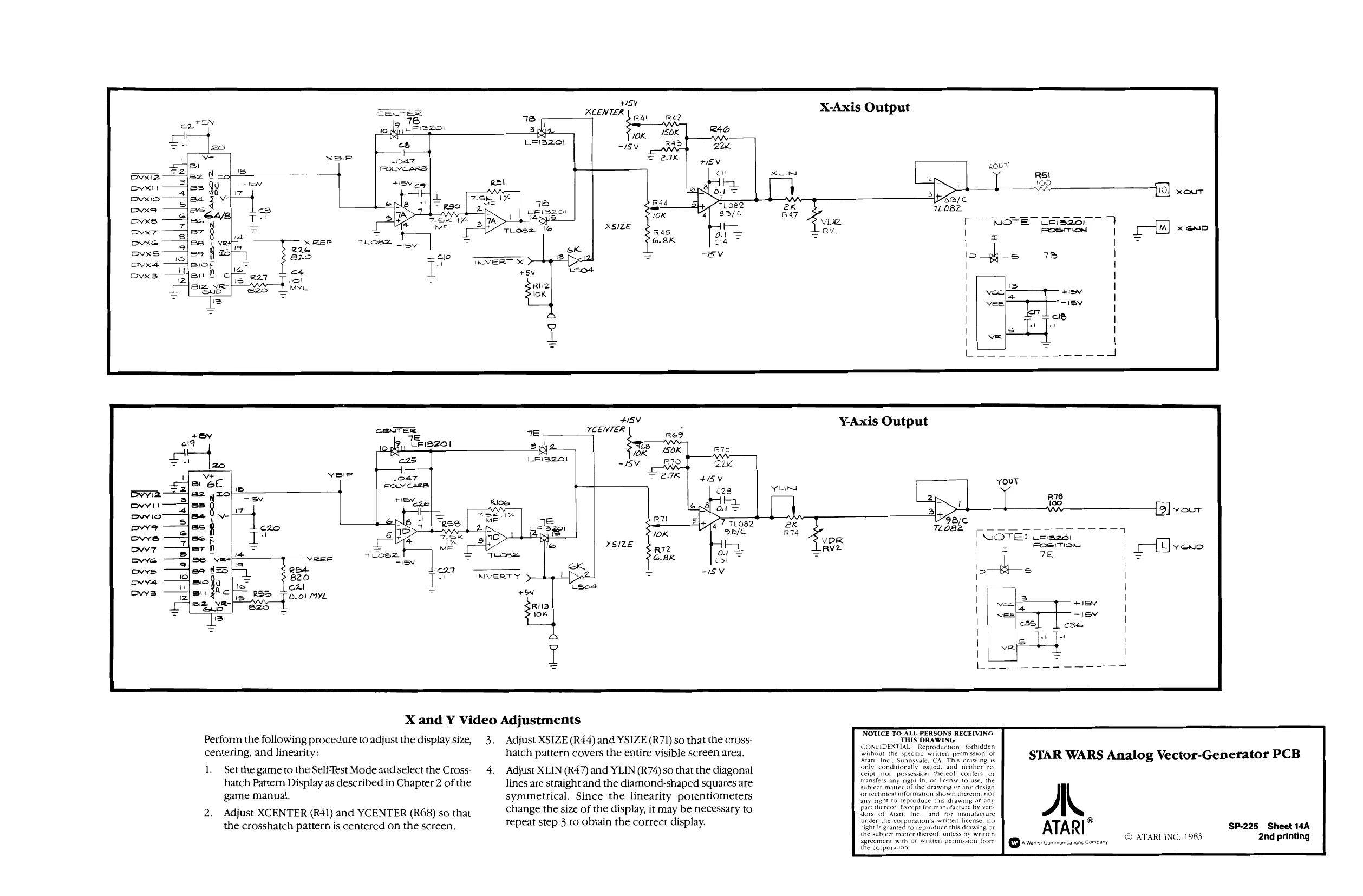
+S XCENTER : Ral Ra?
TER = i “Erazor + Leta2ol
X-Axis Output
t VREF Roy
ead cal is 22 qo ve
YAxis Output
X and Y Video Adjustments
Perform the following procedure to adjust the display size, centering, and linearity:
1. Set the game to the Self-Test Mode and select the Crosshatch Pattern Display as described in Chapter 2 of the game manual.
Adjust XCENTER (R41) and YCENTER (R68) so that the crosshatch pattern is centered on the screen. 3. Adjust XSIZE (R44) and YSIZE (R71) so that the crosshatch pattern covers the entire visible screen area.
Adjust XLIN (R47) and YLIN (R74) so that the diagonal lines are straight and the diamond-shaped squares are symmetrical. Since the linearity potentiometers change the size of the display, it may be necessary to repeat step 3 to obtain the correct display. NOTICE TO ALL PERSONS RECEIVING THIS DRAWING CONFIDENTIAL: Reproduction forbidden without the specific written permission of Atari, Inc., Sunnyvale, CA. This drawing is, only’ conditionally issued, and neither re Ceipt_ nor possession thereof confers or transfers any right in, of license to use, the subject matter Of the drawing or any design Or technical Information shown thereon, n0r any right to reproduce this drawing of any part thereof Except for manufacture by ven. dors of Atari, Inc, and for manufacture Under the corporation's written license, no
right is granted to reproduce this drawing or
the subject matter thereof, unless by written agreement with or written permission from the corporation
STAR WARS Analog Vector-Generator PCB
A. ATARI” © ATARI INC 1983 SP-225 Sheet 14A 2nd printing
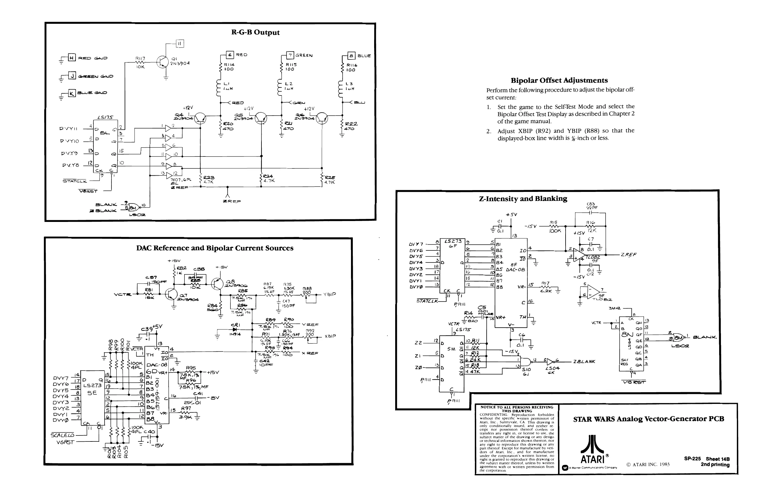
R-G-B Output
i]
Qi 2Nd904
@REEN GND
Bipolar Offset Adjustments
Perform the following procedure to adjust the bipolar offset Current:
- Set the game to the Self-Test Mode and select the Bipolar Offset Test Display as described in Chapter 2 of the game manual.
- Adjust XBIP (R92) and YBIP (R88) so that the displayed-box line width is %-inch or less.
7407 PL Bu ZReEF
Z-Intensity and Blanking
+5V
ir 7S i 1OS a 7 ROL dC ae Ts T
Hae The Ros = RI4 7S, SG x REF Me cA ROS, Pg = 7-BK y 1% MF bP wb is
2 £0 28 ANK 1OPF
NOTICE TO ALL PERSONS RECEIVING "YHIS DRAWING CONFIDENTIAL: "Reproduction forbidden without the specific written permission ‘of | rat Fete cee echoes moe STAR WARS Analog Vector-Generator PCB nly’ conditionally issued, and” nether re
subject matter of the drawing or any design Or technical information shown thereon, nor any right to reproduce this drawing or any
part thereof Except for manufacture by ven:
dors of Atari, Inc., and for manufacture Snder the corporation's written license, no ® wah ig granted reproduce this drawing ot ATARI SP-225 Sheet 14B agement with or writen permission trom | xwamne:Conmuncatons Comoany © ATARI INC. 1983 2nd printing
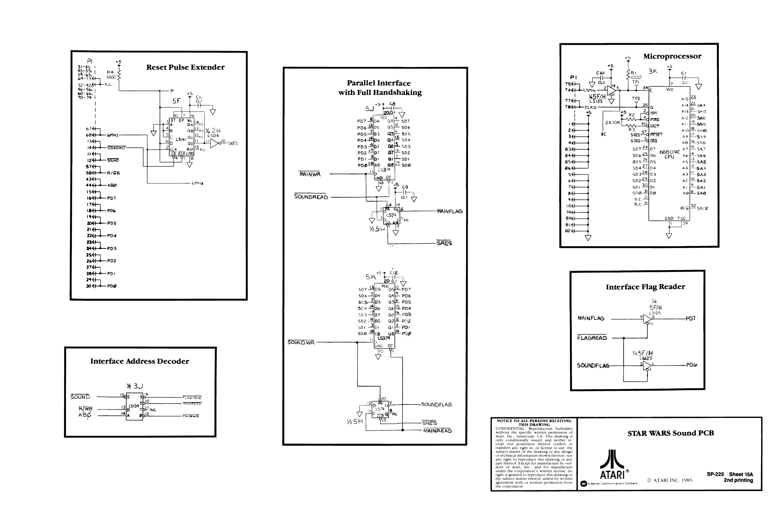
This page is a drawing, shown as the original scan.
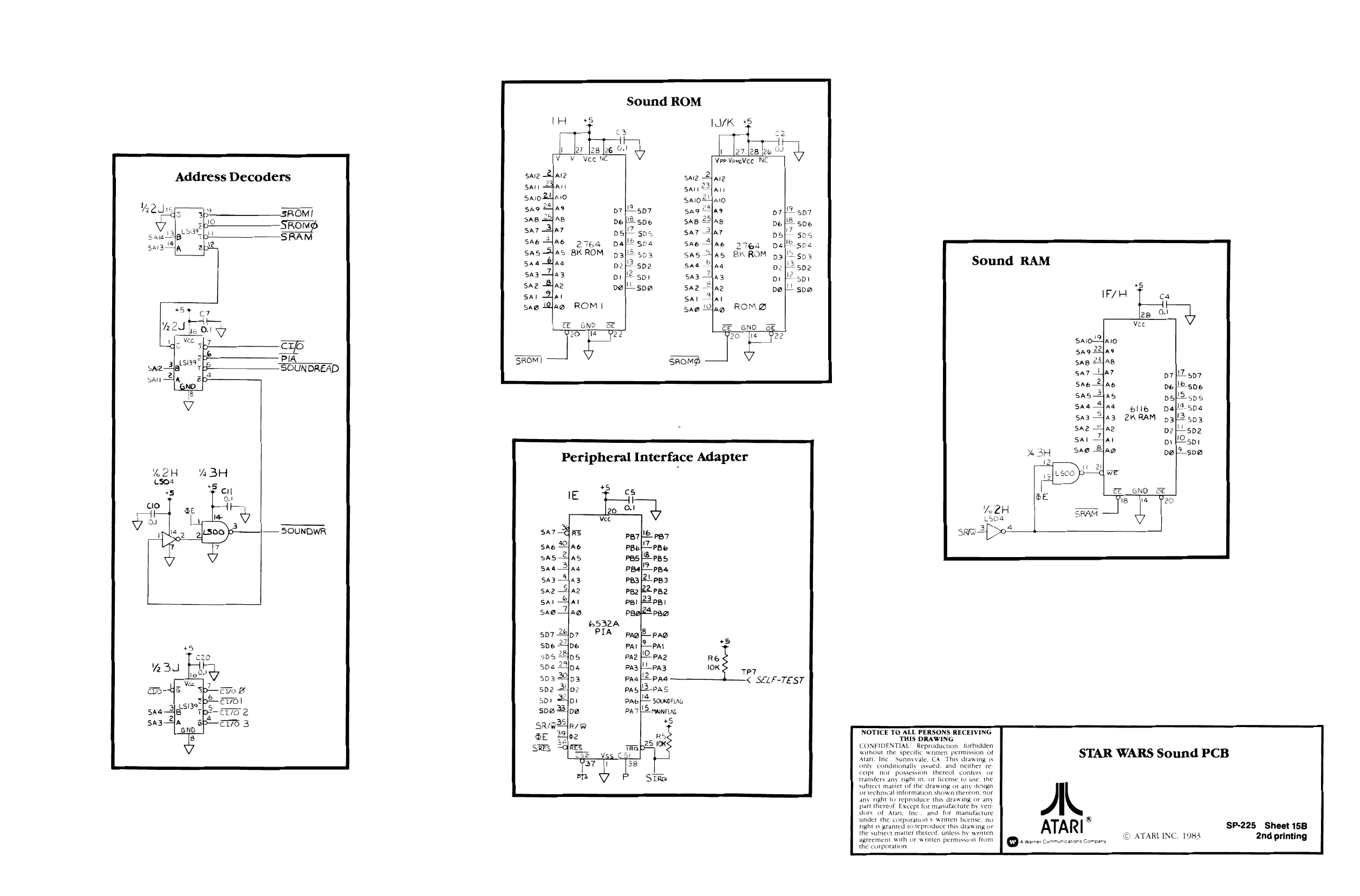
This page is a drawing, shown as the original scan.
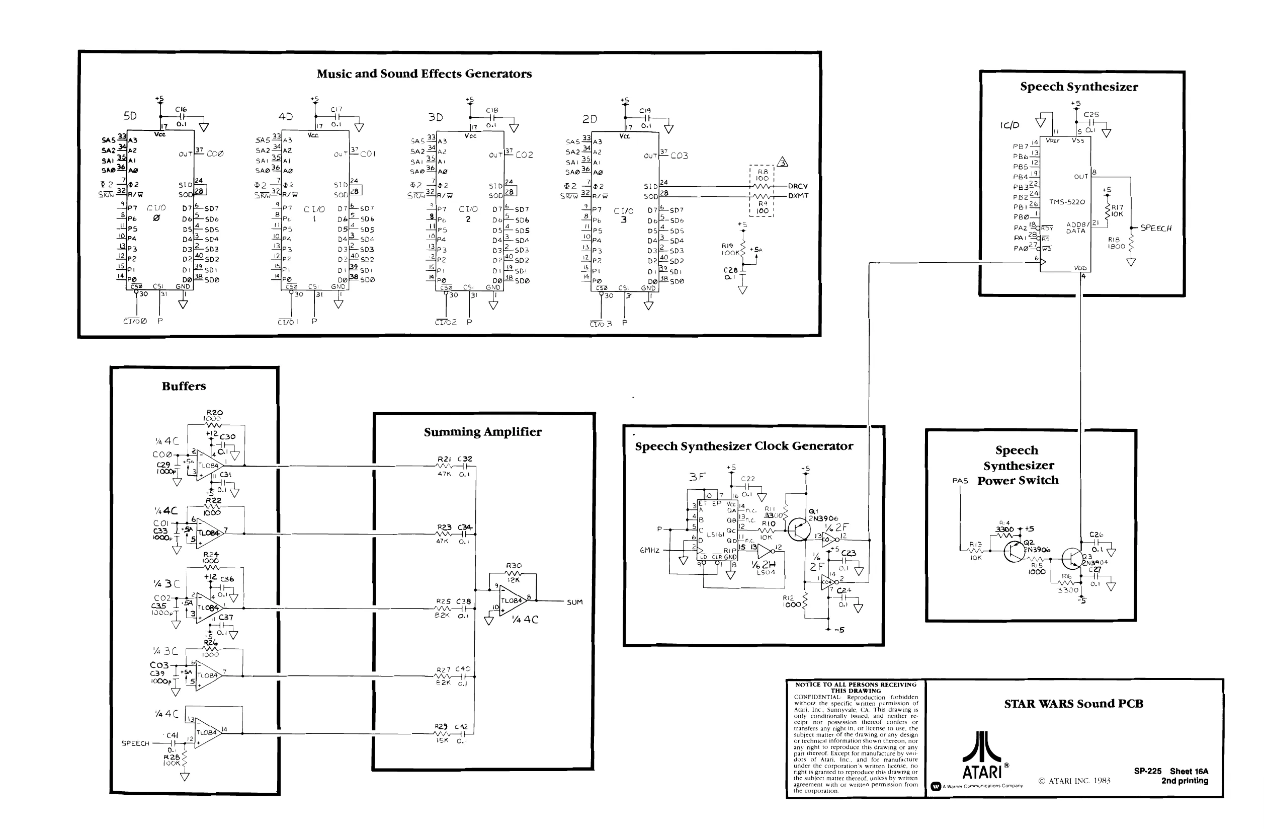
This page is a drawing, shown as the original scan.
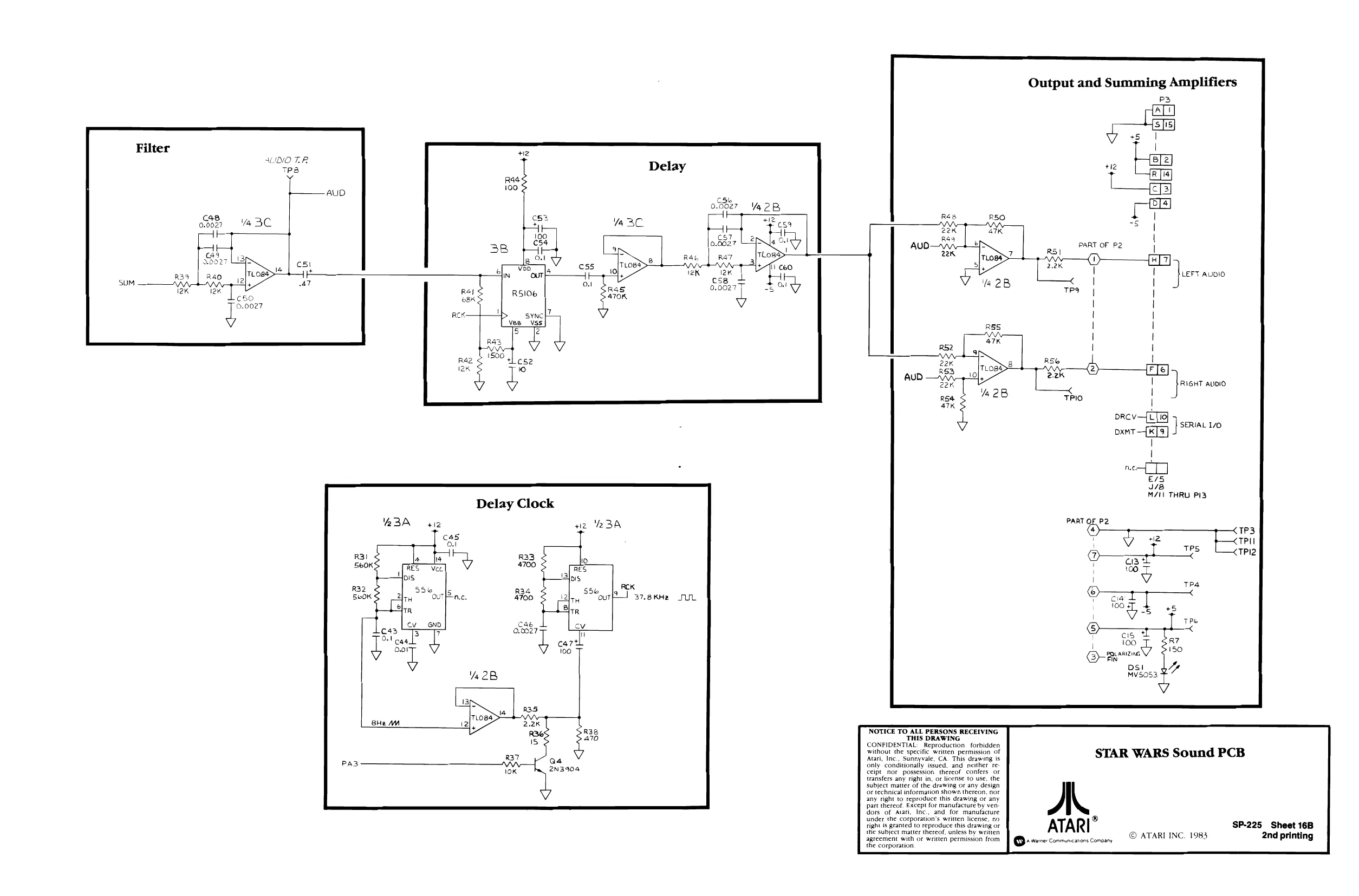
This page is a drawing, shown as the original scan.
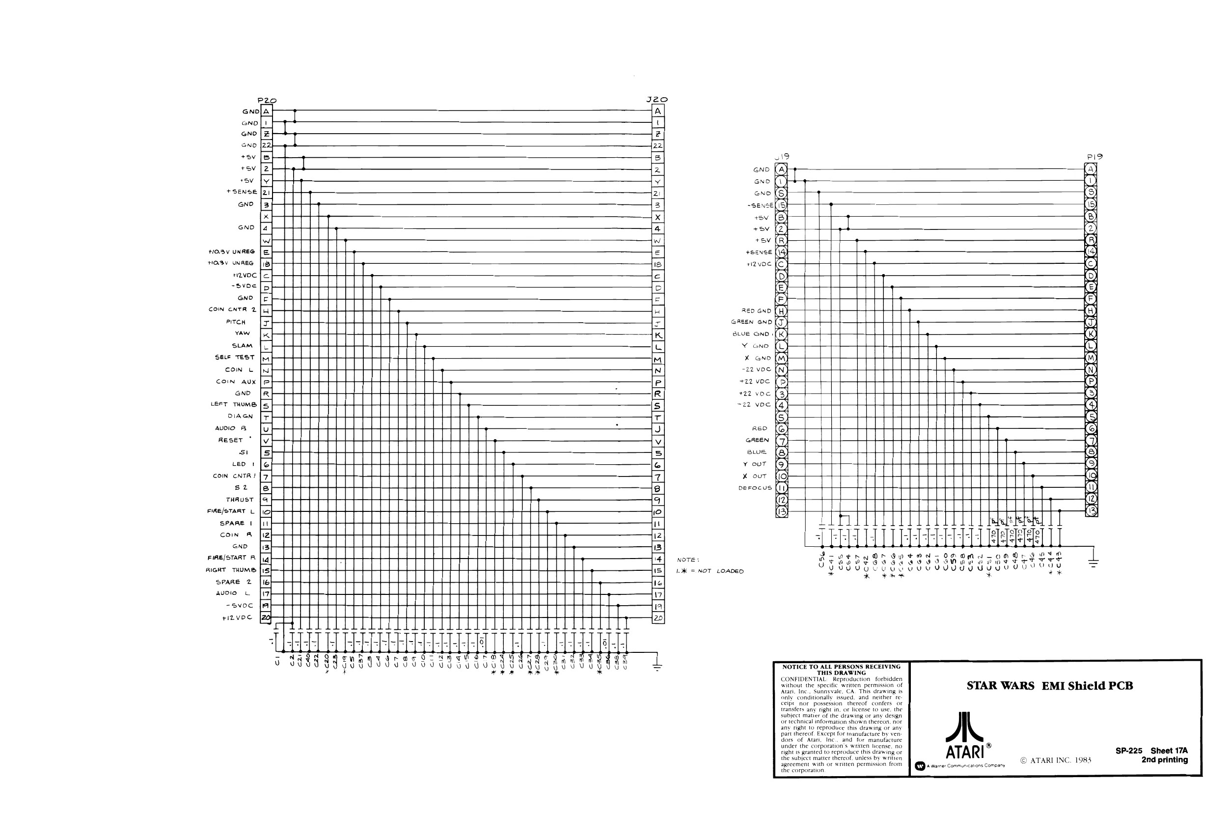
FiRE/START L
SPARE I P20 Jzo eno} A enol f eno [zt z eno [23 22| rev [eS fe rev bet Zz
| sev | [¥ | + | Y |
+sence [zi t+ 2
| eno [at | + | 2 |
| x4 | + | x |
| eno [a | tH | 4 |
Ww Ww.
| rosy uxree [fe | + | z |
rosy uvaee fia) + 16
ravoc fe, + ie
| -svoe [5-4 | 11 | 1 jf. | 5 |
| eno | [Ee | = |
con enta 2 [gq H
| Seco | Co | a |
vaw Tiel }1{1 TK
| stam | [7 | Lt | cL |
| see test [t-+tt | + | mM | |
| conc | fw | + | N |
con aux fe + P
| exo | [Rb | R | |
| Leer Twume fe, | 41 | * | 3 |
owen FELL . =
| avio a | fu | + | J | |
| reser * | [v--+ | +4 | + | 7; |
| s | [5 | + | S |
veo « [e} c
CoN cNTA) [7 7
| sz | fel TTT TT TTT | e |
tHaust [4 9
‘ 1O i, u con
GND
FIRE/START A
RIGHT THUM®
SPARE 2
audio
-svoc
riZvoe sa)
- 13 14 4
te) te [7] v7 Lal fal [20 RED GND
GREEN GND
BLUE GNO+
Y cnp
X GND
-22 vor
+22 voc
+22 voc
-22 voc
RED
GREEN
BWwe
Y ovr
Xx our
DeFocus,
lok = NOT LOADED —+
CJ
a
oO GOOSOOSOOCHGQOG0006
C56 #c41 cas cs4 ces HOST ¥Cce c C42
NOTICE TO ALL PERSONS RECEIVING THIS DRAWING CONFIDENTIAL: Reproduction forbidden without the specific written permission of Atari, Inc., Sunnyvale, CA. This drawing is only conditionally issued, and neither te Ceipt nor possession thereof confers or transfers any right in, oF license to use, th
subject matter of the drawing or any des
Or technical information showa thereon, nor any right to reproduce this drawing or any part thereof Except for snanufacture by ven: dors of Atari, Inc. and for manufacture under the corporation's writen license. no.
right 1s granted to reproduce this drawing or
the subject matter thercof. unless by written agreement with or written permission from the corporation
STAR WARS EMI Shield PCB
A. ATARI” > Ware" Communications Company SP-225 Sheet 17A 2nd printing © ATARI INC. 1983
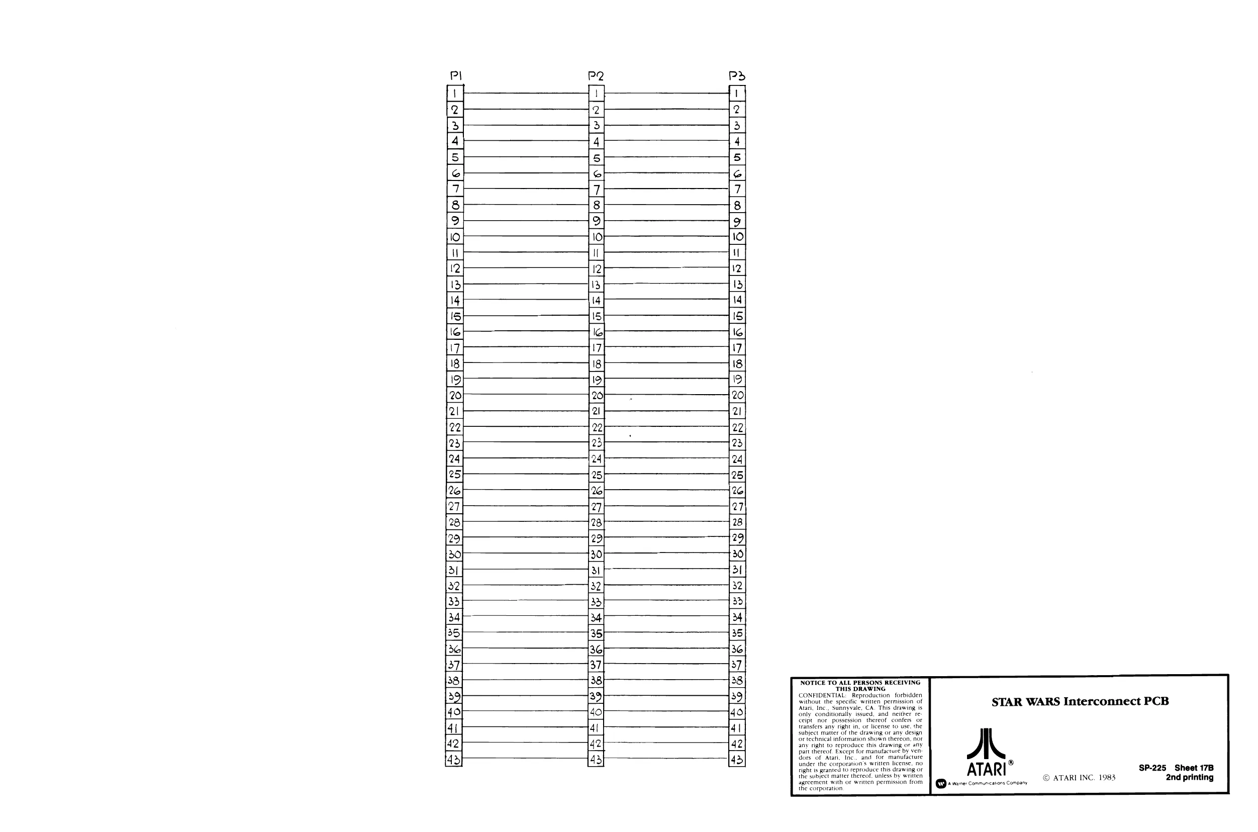
This page is a drawing, shown as the original scan.