PC10 Upright Operation Manual (PCHU-MG5)
PlayChoice Upright (Nintendo, 1990) · Manual · 51 pages · 37 sections · original scan
Play Choice
UPRIGHT NO: PCHU-MG5
OPERATION MANUAL
© 1990 Nintendo’of America Inc.
This equipment generates, uses and can radiate radio frequency energy, and if not installed and used in accordance with the instructions manual, may cause interference to radio communications. It has been tested and found to comply with the limits for a Class A computing device pursuant to Subpart J of Part 15 of FCC Rules, which are designed to provide reasonable protection against such interference when operated in a commercial environment. Operation of this equipment in a residential area is likely to cause interference in which case the user at his own expense will be required to take whatever measures may be required to correct the interference.
Use of non-Nintendo parts or modifications of your Nintendo game circuitry may adversely affect the safety of your game, and may cause injury to your players.
TABLE OF CONTENTS
Il. Location Setup A. Game Installation . B. Voltage Selection . Cc. Power On/Off Switch D. Grounding of Game .... wipe oo
I. Adjustments A. Adjustments of Video Monitor wo
Ml. Maintenance and Repair..... A. Fuse Replacements . B. Cleaning ............ Cc. Operation Panel
- Operation Panel Removal ..
- Micro-Switch Replacement.
- Lubrication of 8-way Controller. D. Front Screen and Video Monitor Removal . E. Game PCB Removal and ROM PCB Exchange .. OCmanARREARA
IV. Radio Frequency Interface
V. Parts List PCHU-MG-5 Game Cabinet Assembly .. PCHU-MG5 Operation Panel Assembly Power Supply Schematic/Parts PCHU-MG5 Wiring Harness . PCK1-CPU PCB Assembly LED PCB Assembly .... K7000 Video Monito
Wiring Diagram - Harness Audio Power Supply/Audio Amplifier ..
INSERTS:
PCK1-CPU Schematics .............eccccccscteeeeseseeeeeeeeteneeeeeeneneeeesenees A-F PCHU-MG5 Wiring Diagram/PCK-01-LED Schematic Monitor Schematics Self Test and Bookkeeping
Check before plugging the game in.
- LOCATION SETUP
Playchoice — Upright is shipped ready for operation. Please check the following to insure proper operation.
- Check the exterior of the game for shipping damage, dents, chips, or broken parts.
- Remove the screws on the rear door panel.
- Unlock and open the rear door panel, as well as the service door, and inspect the interior of the game as follows:
- Check that all the plug-in connectors are firmly connected.
- Check all main subassemblies (monitor, power supply, control panel, etc.) to ensure they are securely mounted.
A. Game installation
- Requirements
Amperage: 1.2 AMPS Temperature: O to 38 degrees Celsius (32 to 100 degrees Fahrenheit) Humidity: Not over 95% relative Space required: 32% x 233/4 Height: 68%
B. Voltage selection for the Video Monitor
Before plugging in your game, make sure the terminal block of the power transformer is correct for your location's line voltage. See figure 1.
Orange 125v ® i+
Red 115v White
Brown _105v
Black Ov Black
+618) 6) O|+ HOS Fig. 1
Cc. Power on/off switch
A power on/off switch is located in the rear of the game at the bottom center of the cabinet.
Please be sure you use a grounded outlet for this game. Failure to do so may result in destruction of electronic components.
D. Grounding of Game (Use only if 3 wire outlet is unavailable.) See Fig. 2
- A grounding wire should be connected to a grounding bar or a metal pipe which is firmly inserted into the ground.
- Do not connect the grounding to a water pipe, because polyvinylchloride pipes are sometimes used in water lines, and the electronic continuity to the ground may be interrupted.
- Absolutely do not connect the grounding wire to a gas pipe, as this can be extremely dangerous.
Fig. 2
I. VIDEO MONITOR ADJUSTMENTS
GREEN DRIVE HORIZ SIZE GREEN CUT OFF
REO ORIVE BLU CUT OFF
RED HORIZ RASTER cut OFF POSITION
D FUSE
‘ TPS TP4 S- TP3
- HV \ sHut-
- 2 “S Down TPI q [ qtee 4 Se Lu GND
-V.SYNC Focus” +> -H.SYNC SCREEN HOBIZ vineo +H. SYNC HORIZ HOLD ae STN
VERT RASTER POS VERT SIZE
VERT HOLD BRIGHTNESS
Do not touch the inside of the Video Monitor.
It contains Many parts supplied with high voltage.
Ill. MAINTENANCE AND REPAIR
A. Fuse Replacements
This game contains 2 fuses. Replace fuses only with the same type as listed below.
Specification of Fuses
- Main Fuse U.S. : 5A 125v/250v
- Video Monitor Fuse 2.0A 125V SB
B. Cleaning
The exterior of the game, all metal parts and all glass parts can be cleaned with a nonabrasive cleanser.
C. Operation Panel
- Operation Panel Removal Before repairing or replacing any switches or 8 way Controllers on the Operation Panel, unplug the game. Open the Service Door, and reach through the opening, and unlock the Clamps, located at each end on the underside of the Operation Panel.
- Micro-switch Replacement Whenever you replace any micro-switch on the Operation Panel, a switch gap adjustment is needed as shown in Fig. 4. This adjustment is not necessary for the player option buttons.
Press
Switch Button Assy.
Fig. 4 Switch gap adjustment
- Lubrication for 8 way Controller To maintain the 8 way Controller in good condition, lubricate the ball socket and 8 way Guide Plate approx. every 3 months. See Fig. 5.
Lubricate here//
Fig. 5 Lubrication points
D. Front Screen and Video Monitor Removal
- Front Screen Removal To remove the Front Screen, first remove the Control Panel by reaching through the Service Door and releasing the Control Panel Clasps. Pull the bottom of the Front Screen toward you allowing it to drop into the slots. Then pull out toward center of game. See Fig. 6
- Video Monitor Removal If you need to remove the Video Monitor, follow the instructions listed below. But the following procedure should only be performed by an experienced service technician.
It is recommended the game be left unplugged for at least one hour before removing the Video Monitor. This will probably discharge the CRT, but extreme caution is still necessary.
- Make sure game is unplugged.
- Remove back door and unplug all the harnesses and cables from the Video Monitor.
- Standing at the front opening of the game, remove the four mounting machine screws and flat washers. See Fig. 7.
- Carefully lift the Video Monitor and pull out toward you.
Use extreme caution and do not touch electrical parts of the yoke area with your hands or with any metal object in your hands.
Remove the four mounting bolts and flat washers
Fig. 7
E. Game PCB Removal
- Make sure the game is unplugged!!
- Open the rear door panel.
- Remove the 36 pin and 44 pin edge connectors from the right side of the FCC-PCBs on the shield cover.
- Pull out the 6 fasteners located on the perimeter of the shield cover. See Fig. 8
- Remove the 56 pin FCC short harnesses from the game P.C. board.
- Remove the game PCB from the shield cage by carefully sliding it straight out of the wooden PCB guides.
(NNN Ill hanging off table
Mw “sewn
SHIELD CAGE xX
062-44P FCC PCB INH Ill Fastener
062-36P FCC PCB
Fig. 8
Areversed connector will damage your PCB! If the connectors don't slip on easily, don’t force them!
IV. RADIO FREQUENCY INTERFERENCE
In order to protect against the RFI radiated from this equipment, please comply with the following. (A) Do not use non-Nintendo parts! (B) Do not modify your game circuitry! (C) Do not modify the wiring harness and connections! (D) Connect this game only to a grounded 3-wire outlet. (E) After servicing the Game PCB, shut the Shield Cover completely with the Fasteners. See Fig. 8. 8
ee
V. REORDER PARTS LIST Cabinet Assembly - Front View (Fig. 9)
| ITEM | ORDERNO. | DESCRIPTION |
| 1 | 19283 | Cabinet |
| 2 | 1088 | Speaker Grill |
| 3 | 3295 | Top Trim |
| 4 | 19050 | Fluorescent Lamp 21" |
| 5 | 10951 | Fluorescent Lamp Only 15w |
| 6 | 19048 | Overlay, Name Plate w/Logo |
| 7 | 1107 | Name Plate Plexi |
| 8 | 3289 | Control Panel Retainer |
| 9 | 593 | T-Molding Black |
| 10 | 576 | Monitor Mtg. Bracket Left |
| a] | 577 | Monitor Mtg. Bracket Right |
| 12 | 6376 | Front Screen (Glass) |
| 13 | 7927 | Control Panel Assy |
| 14 | 3051 | Draw Latch (Control Panel) |
| 15 | 19052 | Door Assy. Complete |
| 16 | 19264 | Coin Selection |
| 17 | 8487 | Coin Slot 25¢ |
| 18 | 19265 | CoinSwitch w/Wire |
| 19 | 19267 | Door Frame |
| 20 | 19268 | Door Lower |
| 21 | 19269 | Door Upper |
| 22 | 19277 | Screw Door Hinge |
| 23 | 19270 | Lock w/Cam |
| 24 | 19053 | Cash Box (plastic) |
| 25 | 11151 | Game Counter |
| 27 | 19064 | Service Switch |
| 28 | 7932 | Side Decal (PCKG) |
| 29 | 19047 | Side Decal Large Logo |
| 30 | 8496 | Led PCB Assy |
| 31 | 3927 | Bracket Led PCB |
| 32 | 4468 | Card Spacer KGLS-4 |
REMARKS
Same as MGSU-01-49
Same as MGSU-01-24
Same as MDSA-01-72 Same as TPPU-01-50 Same as TPPU-01-51 Same as MGSA-01-23 Same as PCKG-23-60
Same as PCKCT-01-09
Same as PCKG-61-12
Same as PCKG-24-01 Same as PCKCT-01-18
This page carries no recoverable text. It is a drawing or a photograph. See the original scan.
Cabinet Assembly - Back View (Fig. 10)
ITEM ORDER NO.
1 7070 2 3050 3 633 4 605 5 8510 6 6888 7 19244 8 1037 9 1034 10 1033 11 612 12 3063 13 455 14 3056 15 19282 16 609 17 1029 18 8931 19 8761 20 8762 21 19127 22 566 23 7054 24 19061 25 19123 26 624 27 450 DESCRIPTION
Back Door Lock Back Door (Key 6510) Key Back Door Only (Key 6510) CamA-Type (BackDoor Lock) PCB PCK1-CPU Assy Shield Cover Cage w/o PCB PCB 44 Pin FCC PCB 36 Pin FCC Fastener Nylatch Fastener Nylatch Grommet Speaker 16 cm 8-ohm Power Cord Strain Relief Bushing Strain Relief Plate Manual, Op Caster Shield Cage Power Supply SA40-1304 Base Power Supply Cover Power Supply ISO Transformer Assy. Bezel, Monitor Bezel, Blind Monitor 19" (Wells Gardner) Audio Amp Assy. Vent Grill Fuse 5A 125v REMARKS
Same as MGSA-01-05 Same as TKGU-01-03 Same as TKGU-01-03-01 Same as TKGU-01-05 Same as PCKU-21-01 Same as MDSU-01-01-11
Same as MDSU-01-01-13 Same as CHPU 23-25 Same as CHPU 23-24
Same as TKGU-01-43 Same as TKGU-01-10 Same as TKGU-01-65
Same as TKGU-01-30 Same as CHPU-01-01-10
Same as MGSP-01-67
Same as TKGU-01-61 Same as TKGU-11-08
Fig. 11
Operation Panel Assembly
| ITEM | PART NO. | ORDER NO. DESCRIPTION | |
| 1 | MDST-14-12 | 773 | 8 Way Control Lever Assembly |
| 2 | TNX-23-18 | 808 | 8 Way Guide Plate |
| 3 | TKGU-23-23 | 813 | E Ring 4 |
| 4 | TKGU-23-21 | 811 | Switch Collar |
| 5 | TKGU-23-22 | 812 | Lever Spring |
| 6 | TKGU-23-20 | 810 | Spring Stopper |
| 7 | TKGU-23-13 | 804 | Micro Switch |
| 8 | TKGU-23-17 | 807 | Switch Spacer |
| 9 | TKGU-23-16 | 806 | Bearing Bracket |
| 10 | TMAU-12-15 | 784 | Lever Plate |
| an} | TMAU-12-14. | 783 | Control Knob Plate |
| 12 | TMAU-12-16 | 785 | Control Knob Collar 8L |
| 13 | TMAU-11-18 | 778 | Knob with Shaft 80.5L |
| 14 | PCKG-12-11 | 7928 | Operation Panel Base |
| 15 | TKGU-23-12 | 803 | Switch Button Bracket |
| 16 | TMAU-34-18 | 821 | Micro Switch VL 12L (Straight) |
| 17 | MDSU-12-17 | 896 | Black Sponge, 2 x 10 x 580L |
| 18 | TKGU-23-26 | 814 | Nut Plate |
| 19 | TKGU-23-34 | 818 | Pal Nut M16 |
| 20 | MDST-12-21 | 932 | Button Assembly (Black) |
| 21 | MDST-12-17 | 854 | Button Assembly (Crimson) |
| 22 | TMAK-11-19 | 865 | Operation Panel Fastener |
| 23 | TMAU-12-18 | 943 | Collar — 34 x 28 x 7H |
| 24 | MDSA-23-31 | 935 | Micro Switch P163C3RU (Red) |
| 25 | MDSA-23-29 | 933 | 062U Switch Collar |
| 26 | MDSA-23-30 | 934 | 062U Switch Bezel |
R a Az R32 Re RS AT RE REO RS RIO RN OR RD fd IS IZ RIG AIT RIB RID AZO API RZZ_AZD AE AIS 27 929 AZO c a ce ca ca ce cy cs ce cn es co cw 23 ci ce CIS CHE CHT C20 CR CI Cat TA " ww we mou re ts 6 ovo o oe a oz 02 04 5 06 07 09 Dm OB ON 03 OF OM on MISC " cer e211 vr
us oO py q 5 19
i 16 ca | ‘pee ‘Pezop ora 12 | +—4 : LJ oz Ly ‘THE DRAWING AND SPECIFICATIONS HENEIN ARE THE PROPERTY OF ASTEC U.S.A. AND SHALL NOT BE REPRODUCED OR COPIED OR USED IN WHOLE OR PART AS THE BASIS FOR THE MANUFACTURE OR SALE OF ITEMS WITHOUT WRITTEN PERMISSION.
(UD ROT STALE URAMING IDANNY NG ze.seP
CIRCUIT DIAGRAM
= cs Pant wo Cuan 25.48m _ mere om Tinie 2 [hoo ore CELETE Cz RIE ADT cons. 26.14.85] REL. DRAWING NOTE: THIS RFI EASED DRAs.ING WAS PRODUCED BY COMPUTER, DO NOT UPDATE MASTER MANUALLY. one Kone sw bor REVISIONS,
“T_ f
Power Supply (SA40-1304)
ORDER NO. DESCRIPTION (REFERENCE DESIGNATIONS & LOCATIONS)
| 18317 | RECTIFIER, DIODE RGP 10B | D9 | ||
| 18318 | RECTIFIER, DIODE1N 4001 GP | D12-13 | ||
| 18319 | RECTIFIER, DIODE GP10A | D3 | ||
| 18320 | RECTIFIER, BRIDGE KBP08 | DB1 | ||
| 2076 | RES, CARBON 10 OHM 1/4 W 5% | R10-R28-R32 | ||
| 2078 | RES, CARBON 1/4 W 5% | R5 | ||
| 18321 | RES, CARBON 15 OHM 1/4 W + 5% | R11 | ||
| 2103 | RES, CARBON 22 OHM 1/4 W 5% | R27 | ||
| 2111 | RES, CARBON 27 OHM 1/4 W 5% | R8& | ||
| 2112 | RES, CARBON 270 OHM 1/2 W + -5% | R15-R16 | ||
| 2121 | RES, CARBON 330 OHM 1/4 W 5% | R18-R21 | ||
| 7247 | RES, CARBON 47 OHM 1/4 W 5% | Ri4 | ||
| 2133 | RES, CARBON 470 OHM 1/4 W 5% | R22 | ||
| 2136 | RES, CARBON 470K OHM 1/2 W 5% | Ri | ||
| 4713 | RES, CARBON 56 OHM 1/4 W 5% | R19 | ||
| 18322 | RES, CARBON 5.6 OHM 1/4 W + /-5% | R13 | ||
| 2148 | RES, CARBON 68 OHM 1/4 W 5% | R20-R9 | ||
| 18323 | RES, CARBON 8.2 OHM 1/4 W + /-5% | R17 | ||
| 18324 | RES, M.FILM .75 OHM 1 W + /-5% | R12 | ||
| 18325 | RES, M.FILM 1 OHM 1 W + /-5% | R7 | ||
| 18326 | RES, M.FILM 18 OHM 1/4W + /-1% | R25 | ||
| 18327 | RES, M.FILM 2.7 OHM 1/4W + /-1% | R24 | ||
| 18328 | RES, M.FILM 8.2 OHM 1/4W + /-1% | R23 | ||
| 1997 | RES, OXIDE 100K OHM 1 W + /-5% | R3-R4 | ||
| 18239 | RES, OXIDE 120 OHM 2 W + /-5% | R6-R29 | ||
| 18330 | RES, WIRE WD 15 OHM 5 W + /-5% | R30 | ||
| 18331 | RES, WIRE WD 330HM 3 W | + | /-5% | R2 |
| 18292 | CAP, CERAMIC 100 PF 3KV + /-20% | cg | ||
| 18293 | CAP, CERAMIC .01 MF 100V + 80 - 20% | C23 | ||
| 18294 | CAP, CERAMIC 330P 100V + /-20% | C18 | ||
| 18295 | CAP, ELECTRO 100 MF 25V + /-20% RADIAL | C14 | ||
| 18296 | CAP, ELECTRO 1000 MF 16V + /-20% RADIAL | c20 | ||
| 18297 | CAP, ELECTRO 1000 MF 10V+ /-20% RADIAL | C15 | ||
| 18298 | CAP, ELECTRO 100 MF 10V + /-20% RADIAL | C17 | ||
| 18299 | CAP, ELECTRO 220 MF 10V+ 100 - 10% RADIAL | c8 | ||
| 18300 | CAP, ELECTRO 2200MF 16V + /-20% RADIAL | C12 | ||
| 18301 | CAP, ELECTRO 470 MF 16V + /-20% RADIAL | C19 | ||
| 18302 | CAP, POLYESTER .01 MF 50V +/-5% | C13 | ||
| 18303 | CAP, MP .1 MF 250V + /-20% | C1-C2 | ||
| 18304 | CAP, POLYESTER 2200P 250V + /-20% | C3-C4 | ||
| 18305 | CAP, POLYESTER .022 MF SOV + /-20% | C16 | ||
| 18306 | CAP, MP 0.022 MF 250V + /-20% | C10 | ||
| 18307 | CAP, POLYESTER .22 MF 100V + /-20% | c11-C21 |
Power Supply (SA40-1304) - continued
ORDER NO. DESCRIPTION (REFERENCE DESIGNATIONS & LOCATIONS}
18308 18309 18310 7161 18311 18312 18313 18314 18315 18316 18322 18333 18334 18335 18336 18337 18338 18339 18340 18341 18342 18343 18344 18345 CAP, MPR 2200P 250V = /-20% FUSE, F2A 250V (SA40-1304) CONN. 4 PIN (SA40-1304 TRANSISTOR, 2SC 2120 TRANSISTOR, 2SB 561 REGULATOR, 431 DIODE, SI IN4606 DIODE, ZENER 5.6V 240 MA + /-5% RECTIFIER, DIODE RGP10A RECTIFIER, DIODE RGP10J RES, VARIABLE 1K OHM TOP ADJUST THERMIST, 84 + /-20% COIL, CHOKE 1.5 MH COIL, CHOKE 2.2 UH TRANSFORMER, CONTROL ASSY TRANSFORMER, POWER AC8154 TRANSFORMER, COM MODE ASSY COIL, CHOKE ASSYO COIL, CHOKE FILTER RECTIFIER, HEAT SINK ASSY TRANSISTOR, 2SD1494 HEAT SINK ASSY REGULATOR, UA7912 DIODE, SKCE 12CTQ035 SCR, 2N6395 C5 FA TB2 Qi Q3 1C1 D11-D6-D7
D1 D2-D4-D5 VRI TMI-TM2
Wiring Harness
ORDER NO.
2357 2356 8968 7933 2337 7934 19107 19109 19116 19106 19101 19102 19114 19259 19105 19129 19128 19099 19103 19110 19111 19112 19113 19117 19118 19119 19120 DESCRIPTION REMARKS
44 Pin FCC Harness Same as MDSU-41-12 36 Pin FCC Harness Same as MDSU-41-11 44 Pin Edge Connector Harness Same as MGSU-41-13 36 Pin Edge Connector Harness Same as PCKG-41-11 15 Pin Switch Harness Same as MGSU-42-11 12 Pin Switch Harness Same as PCKG-41-11 Audio PCB Harness Coin Counter Harness Service Switch Harness 9 Pin Power Harness (Astec) 2 Pin Lamp Plug 3 Pin Monitor Power Supply AC Harness (Astec) 12v Power Supply AC Harness 6 Pin Video Harness Transformer Assembly Harness 4 Pin Coin Harness 2 Pin AC Input Harness 3 Pin Transformer Harness Fuse Harness (Black) Noise Filter Harness (Black) Noise Filter Harness (White) Noise Filter Harness (Green) Terminal Block Harness (Black) Terminal Block Harness (Red) Terminal Block Harness (Brown) Terminal Block Harness (Orange)
Main PC Board
PART NO.
PCKU-21-01 PCHU-21-11 PCHU-21-12 PCHU-21-13 PCKU-21-14 PCKU-21-15 PCKU-21-16 PCKU-21-17 PCHU-21-18 PCHU-21-19 PCHU-21-20 PCKU-21-21 PCKU-21-22 PCKU-21-23 PCHU-21-24 PCHU-21-25 PCHU-21-26 PCHU-21-27 PCHU-21-28 PCHU-21-29 PCHU-21-30 PCHU-21-31 PCHU-21-32 PCHU-21-33 TPP2-06-20 PCHU-21-34 PCHU-21-35 PCHU-21-36 PCHU-21-37 PCHU-21-38 PCHU-21-39 PCHU-21-40 PCHU-21-41 PCHU-21-42 PCHU-21-43 PCHU-21-44 PCHU-21-45 PCHU-21-46 PCHU-21-47 PCHU-21-48 PCHU-21-50 PCHU-21-51 PCHU-21-52 PCHU-21-53 PCHU-21-54 PCHU-21-55 PCKU-21-55 PCHU-21-56 PCHU-21-57 ORDER NO.
7929
4460 7936 7937 7938 7939 2060 2061 4811 7940 7941 7942 2189 2190 2191 2193 2195 2196 2202 2203 2204 2205 2208 2210 2216 2220 2223 2225 2226 2228 2229 2230 2232 2233 2235 2239 2242 2243 2247 2267 2259 2278 4812 8004 1143 1445, 1443 DESCRIPTION (Reference Designations and Locations)
PCK1 CPU Complete PCB Assembly Z80A Microprocessor RP2A03E Microprocessor RP2C03B PPU 27128 16K-Byte EP-ROM 300ns PCK 1-C-8T 2764 8K-Byte EP-ROM 300ns PCK 1-C-8K 2764 8K-Byte EP-ROM 300ns PCK 1-C-8M 2764 8K-Byte EP-ROM 300ns PCK 1-C-8P TMM2115BP-15 2K-Byte RAM 150ns HM6116 ASP-20 2K-Byte RAM 200ns TC5517 CPL-20 2K-Byte C-MOS RAM 200ns N82SI29N 256x4-Bit Bipolar ROM PCK1-C-6D N82SI29N 256x4-Bit Bipolar ROM PCK1-C-6E N82SI29N 256x4-Bit Bipolar ROM PCK1-C-6F 74LS00 Quad 2-Input NAND 74LS02 Quad 2-Input NOR 74LS04 Hex Inverters 74LS08 Quad 2-Input AND 74LS11 Triple 3-Input AND 74LS14 Hex Schmitt Inverters 74LS32 Quad 2-Input OR 74LS42 4 To 10 Decoders 74LS55 2-Wide 4-Input AND-OR-INVERT Gates 74LS74A Dual "D" Flip-Flops (P, CL) 74LS86 Quad 2 Input EX-OR 74LS109A Dual J-K Flip-Flops (PLE, CL) 74LS139 Dual 2 To 4 Decoders 74LS157 Quad 2 To 1 Data Selectors 74LS161A 4-Bit Binary Counters 74LS164 8-Bit Shift Registers 74LS165A 8-Bit Shift Registers 74LS175 Quad "D" Flip-Fips (CL) 74LS194A 4-Bit Shift Registers 74LS240 Octal Bus Inverters (TS) 74LS244 Octal Buffers & Line Drivers (TS) 74LS245 Octal Bus Transceivers (TS) 74LS259 8-Bit Addressable Latches 74LS299 8-Bit Shift/Storage Registers 74LS367A Hex Bus Drivers 74LS368A Hex Bus Drivers 74LS377 Octal "D" Flip-Flops 74804 Hex Inverters 7437 Quad-2-Input NAND Buffers 75471 Dual Peripheral AND Drivers 74HC10 Triple 3-Input NAND C-MOS TC74HC373 Octal 3-State D-Latches C-MOS PST518A Low Voltage Detector LM324 Quad Operational Amplifiers LM3900 Quad Operational Amplifiers (5X) (1H) (3H) (8T) (8K) (8M) (8P) (2k) (4K, 8R, 8V) (8W) (6D) (6E) (6F) (5H, 8J, 6U) (4U) (8D, 3G, 8G, 5J, 7R,7Y, 42) (7X) (5P) (4V) (7C, 5T) (47) (5K) (7J, 7K, 5M) (4M) (4Y) (7H, 2L, 6T) (78, 7T, 7U, 7V) (6H, 6J, 6K, 6L, 6M, 4R) (8H, 5Q) (8B, 8C, 7F) (48) (6Q, 6R) (5A, 6A, 7B) (6B, 1L, 2M, 3M, 8S, 5V, 6V) (1K, 62) (7D, 7E) (7L, 7N, 7Q) (4L) (8E, 8F, 5S) (6P) (2G, 6N) (4X) (6C) (8Y) (3k) (72) (3E) (1E)
Main PC Board - continued
| PART NO. | ORDER NO. | DESCRIPTION (Reference Designations and Locations) | ||
| PCKU-21-57 | 7943 | TC 4053BP Triple 2-Channel Multiplexer C-MOS | (5C) | |
| PCHU-21-58 | 735 | CD 406 6B Quad Analog Switches C-MOS | (3C) | |
| PCHU-21-59 | 2178 | 2SA933 Silicon PNP Tansistor | (Q11,Q12,Q14,Q15, Q17, Q18) | |
| PCHU-21-60 | 2179 | 2SA1015 | Silicon PNP Transistor | (Q3, Q5, Q7, Q20) |
| PCHU-21-61 | 2184 | 2SC1740 Silicon NPN Transistor | (Q8~Q10, Q13, Q16, Q19, Q20~Q26) | |
| PCHU-21-62 | 2185 | 2SC1815 | Silicon NPN Transistor | (Q1, Q2, Q4, Q6) |
| PCHU-21-63 | 1003 | ES1F | Diode | (D1) |
| PCHU-21-64 | 1012 | 1S5277B Diode | (D3, D4) | |
| PCHU-21-65 | 4813 | EG01Y | Diode | (D2) |
| PCHU-21-66 | 1002 | DAN401 Quad Cathode-Common Diode Array | (DA1~DA8) | |
| PCHU-21-67 | 4817 | 1.0f5.5V Electric Double Layer Capacitor (EEC F5R5U105) | (C3) | |
| PCHU-21-68 | 680 | 68pf 50V Ceramic-Disc Capacitor | (C44) | |
| PCHU-21-69 | 663 | 100pf 50V Ceramic-Disc Capacitor | (C35, C36, C45, C71) | |
| PCHU-21-70 | 669 | 180pf 50V Ceramic-Disc Capacitor | (C11, C39) | |
| PCHU-21-71 | 675 | 330pf 50V Ceramic-Disc Capacitor | (C2, C6, C40, C41) | |
| PCKU-21-71 | 7945 | 470pf 50V Ceramic-Disc Capacitor | (C12) | |
| PCHU-21-72 | 664 | 1000pf 50V Ceramic-Disc Capacitor | (C5) | |
| PCHU-21-73 | 665 | 0.01uf 50V Ceramic-Disc Capacitor | (C4, C22, C38, C43, |
C80~C83, C86~C89, C91, C92, C94~C101, C103~C108, C110~C 120, C122~C126, C128, C130~C144, C146, C148~C156, C158~C163, C165~C187)
| PCHU-21-74 | 4815 | 0.047uf 50V Ceramic-Disc Capacitor | (C15~C17) |
| PCHU-21-75 | 655 | 0.2uf 12VCeramic-Disc Capacitor | (C21) |
| PCHU-21-76 | 716 | 0.047uf 50V Film Capacitor | (C33, C34) |
| PCHU-21-77 | 685 | 1uf 16V Al Electrolytic Radial Cap. | (C7, C8) |
| PCHU-21-78 | 689 | 3.3uf 16V Al Electrolytic Radial Cap. | (C13, C14, C25, C28, C31, C32) |
| PCHU-21-79 | 683 | 10uf 16V Ai Electrolytic Radial Cap. | (C23, C24, C26, C27, C29, C30, C37, |
C42)
| PCHU-21-80 | 688 | 33uf 16V Al Electrolytic Axial Cap. | (C9) |
| PCHU-21-81 | 4818 | 47uf 16V Al Electrolytic Radial Cap. | (C47~C50) |
| PCHU-21-82 | 684 | 100uf 16V Al Electrolytic Axial Cap. | (C46) |
| PCHU-21-83 | 4819 | 100uf 25V Al Electrolytic Axial Cap. | (C70) |
| PCHU-21-84 | 687 | 220uf 16V Al Electrolytic Axial Cap. | (C1) |
| PCHU-21-85 | 691 | 470uf 16V Al Electrolytic Axial Cap. | (C20) |
| PCHU-21-86 | 4820 | 3.3uf 16V Tantalum Electrolytic Cap. | (C85, C90, C93, C102, |
C109, C121,C127,C145, C157)
| PCHU-21-87 | 2075 | 0 Ohm Shunt Lead | (R99) |
| PCHU-21-88 | 2076 | 10 Ohm 1/4W + 5% Resistor | (R7) |
| PCHU-21-89 | 2120 | 33 Ohm 1/4W— 5% Resistor | (R32, R37) |
| PCHU-21-90 | 2137 | 51 Ohm 1/4W—-5% Resistor | (R8, R19, R23, R27, R31) |
| PCHU-21-91 | 2077 | 100 Ohm 1/4W + 5% Resistor | (R17, R68, R69, R73) |
| PCHU-21-92 | 2082 | 110 Ohm 1/4W —-5% Resistor | (R3) |
| PCHU-21-93 | 2121 | 330 Ohm 1/4W —-5% Resistor | (R13, R14, R18, R21, R25, |
R29, R36, R90, R91, R97, R98, R110, R111, R112)
| PCHU-21-94 | 2138 | 510 Ohm 1/4W — 5% Resistor | (R46, R56, R66) |
| PCHU-21-95 | 2155 | 820 Ohm 1/4AW— 5% Reisstor | (R1, R2) |
| PCHU-21-96 | 2078 | 1K Ohm 1/4W —- 5% Resistor | (R94~R96, R120~R131) |
| PCHU-21-97 | 2099 | 2K Ohm 1/4W 5% Resistor | (R15, R87, R109) |
| PCHU-21-98 | 2105 | 2.2K Ohm 1/4W + 5% Resistor | (R35, R40, R42, R50, R45, |
R52, R55, R60, R62, R65)
| PCHU-21-99 | 2134 | 4.7K Ohm 1/4W — 5% Resistor | (R43, R53, R63) |
| PCHU-21-100 | 2139 | 5.1K Ohm 1/4W — 5% Resistor | (R4 ,R5, R22, R26, R30, |
R88, R89)
| PCHU-21-101 | 2152 | 7.5K Ohm 1/4W — 5% Resistor | (R16) |
Main PC Board - continued
(R12, R34, R38, R41, R44, R51, R54, R61, R64, R74, R82, R83, R92, R93, R100~R102, R104, R106, R108) (R71) (R6, R39, R70, R72, R103, R, 105, R107) (R33, R75) (R9~R11) (R79) (R78, R80, R84) (R76, R85) (R81) (R77, R86) (RM1, RM16) (RM5, RM8~RM10, RM13) (RM6, RM7, RM11, RM12, RM14, RM15) (RM2~RM4) (VR1) (VR2) (VR3) (x1) (X2, X3) (SW1, Sw2) (SW) (S6~S8) (S2~S5) (S1, $9, $10) (CH1~CH10)
| PART NO. | ORDER NO. | DESCRIPTION (Reference Designations and Locations) |
| PCHU-21-102 | 2079 | 10K Ohm 1/4W -_5% Resistor |
| PCHU-21-103 | 2086 | 12K Ohm 1/4W 1.5% Resistor |
| PCHU-21-104 | 2100 | 20K Ohm 1/4W 15% Resistor |
| PCHU-21-105 | 2080 | 100K Ohm 1/4W- 5% Resistor |
| PCHU-21-106 | 2101 | 200K Ohm 1/4W 5% Resistor |
| PCHU-21-107 | 2126 | 360K Ohm 1/4W +-5% Resistor |
| PCHU-21-108 | 2154 | 750K Ohm 1/4W +-5% Resistor |
| PCHU-21-109 | 2081 | 1M Ohm 1/4W.5% Resistor |
| PCHU-21-110 | 2097 | 1.8M Ohm 1/4W= 5% Resistor |
| PCHU-21-111 | 2107 | 2.2M Ohm 1/4W__ 5% Resistor |
| PCHU-21-112 | 2068 | Hex 5.1K Ohm Series Resistor Array |
| PCHU-21-113 | 2065 | Octal 1K Ohm Series Resistor Array |
| PCHU-21-114 | 2071 | Quad 68 Ohm Parallel Resistor Array |
| PCHU-21-115 | 4821 | NT-01 Resistor Array |
| PCHU-21-116 | 2290 | 500 Ohm Variable Resistor, Red Cap |
| PCHU-21-117 | 2289 | 500 Ohm Variable Resistor, Green Cap |
| PCHU-21-118 | 2279 | 500 Ohm Variable Resistor, Blue Cap |
| PCHU-21-119 | 2411 | 8MHZ Crystal |
| PCHU-21-121 | 2414 | 21.47727 MHz Crystal |
| PCHU-21-123 | 2174 | 8-Station, Single-Throw, DIP Bit Switch |
| PCHU-21-124 | 4823 | MINI-BIT Header |
| PCHU-21-125 | 2166 | 16 Pin DIP IC Socket |
| PCHU-21-126 | 2171 | 28 Pin DIP IC Socket |
| PCHU-21-127 | 2172 | 40 Pin DIP IC Socket |
| PCHU-21-129 | 4880 | 96 Pin DIN Connector Receptacle |
| PCHU-21-130 | 4825 | GL-3HD1 Visible Light Emitting Diode |
at (LED1)
PCK 1 - LED PCB Assembly
PART NO. ORDER NO. DESCRIPTION (Reference Designations )
| PCKU-24-11 | 7947 | 74HCT138 3 TO 8 Demultiplexer |
| PCKU-24-12 | 7948 | LR74HC4511/TC74HC4511P |
BCD to 7 Segment Latch Decoder /Driver
| TPP2-07-32 | 7142 | 1$5277B Diode |
| TPP2-07-33 | 1002 | DAN401 Quad Cathode-Common Diode Array |
| CHPU-22-56 | 663 | 100 pf. 50V Ceramic-Disc Capacitor |
| CHPU-21-62 | 665 | 0.01 uF 50V Ceramic-Disc Capacitor |
| TPP2-07-39 | 688 | 33uF 16V Al Electrolytic Axial Cap. |
| TPP2-07-63 | 2065 | Octal 1K Ohm Series Resistor Array |
| PCKU-24-16 | 7950 | El 12 pin Plug Connector Right Angle |
| PCKU-24-17 | 7949 | GL-8E040 7-Segment Visible Light Emitting Diode |
(US)
(U1~U4) (D1~D3) (DM1) (C7~C10) (C2~c6) (C1) (RM1) (P1) (LED1~LED4)
K700 Monitor Parts
PART NO. ORDER NO. DESCRIPTION
| MON-20-01 | 8558 | IC, Regulator STR 3123 |
| MON-20-02 | 8559 | IC, Video UPC 1397 NEC |
| MON-20-03 | 8560 | IC, Horiz Vert LA7823 |
| MON-20-04. | 8561 | IC, Vert Output UPC 1378 |
| MON-21-01 | 8562 | Diode, D1 Fast SW RU-2 |
| MON-21-02 | 8563 | Diode, S1 1A 600v |
| MON-21-03 | 8564 | Diode, GFE 10R |
| MON-22-01 | 8565, | Transistor, NPN CC. |
| MON-22-02 | 8566 | Transistor, 2SD1398 |
| MON-22-03 | 8567 | Transistor, 2SC2068 |
| MON-23-01 | 8568 | Coil, Width — TODAI |
| MON-23-02 | 8569 | Coil, Lin — TODAI |
| MON-24-01 | 8570 | Transformer, Flyback |
| MON-24-02 | 8571 | Transformer, Horiz Driver |
| MON-25-01 | 8572 | Res, Variable 2K ohm |
| MON-25-02 | 8573 | Res, Variable 10K ohm |
| MON-25-03 | 8574 | Res, Variable 200 ohm |
| MON-25-04 | 8575 | Res, Variable 200K ohm |
| MON-25-05 | 8576 | Res, Variable 100 ohm |
| MON-25-06 | 8577 | Res, Trim Pot 2K ohm 0.3w |
| MON-25-07 | 8578 | Res, Trim Pot 200 ohm |
| MON-26-01 | 8579 | Cap, Electrolytic 1.0 UF 50V |
| MON-26-02 | 8580 | Cap, Electrolytic 10 UF 25V |
| MON-26-03 | 8581 | Cap, Electrolytic 22 UF 160v |
| MON-26-04 | 8582 | Cap, Electrolytic 47 UF 25V |
| MON-26-05 | 8583 | Cap, Electrolytic 470 UF 516V |
| MON-26-06 | 8584 | Cap, Electrolytic 1000 UF 16V |
| MON-26-07 | 8585 | Cap, Electrolytic 1000 UF 25V |
| MON-26-08 | 8586 | Cap, PolyPro PP6100 2% 1500V |
| MON-26-09 | 8587 | Cap, PolyPro .39 UF 5% 200V |
| MON-26-10 | 8588 | Cap, .1 20% 125v AC |
| MON-26-11 | 8589 | Cap, Disc .0015 10% 500v |
| MON-26-12 | 8590 | Cap, Disc .0022 10% 500v |
| MON-27-01 | 8591 | Res, M. Oxide 3.9K 5% |
| MON-27-02 | 8592 | Res, 2.7 ohm 5% 7w |
| MON-27-03 | 8593 | Res, Thermister |
| MON-28-01 | 8594 | Fuse, 1.5A |
| MON-29-01 | 8595 | Plug, 2 Pin |
| MON-29-02 | 8596 | Plug, 4 Pin |
| MON-30-01 | 19279 | Picture tube, 19" (Wells-Gardner) |
| MON-30-02 | 19280 | Yoke, Deflection (Wells-Gardner) |
| MON-30-03 | 19281 | Coil, Degaussing (Wells-Gardner) |
] {
Pck-cPU
PC, BOARD
i
/
| 1
} {
it
ee ees | iz TIP RIGHT a [13 7 ip terry a 062A 44P FCC P.C, BOARD el
fos izelrS |
Ele
062 36P FCC P.C, BOARD
aon
ai |e |= =a)
fl
WIRING DIAGRAM
DRAWN BY H. KAMADA. DATA:02/07/90 | APPROVED BY: MODEL: PCK-UP FCC HARNESS
Nintendo of America
44P Edge Harness Connector
36P Edge Harness Connector
Audio Power Supply
ren K+ PSCRT SSS ee ieee Oa crea: RE Son
- oO pA Quvour cre Lor *
—fon 12 303 7
| o | Les | ut | c# | Rs | kts | Bore | SR0 |
2 6 5 7 i
chert fcr Re for RO 4 Lady | 4 —-;——O-our
‘copied or used In whole or part the esl for the manufacture L OC sale of Nome wRhow writen permlaslon, - os
Audio Amplifier
aus CE aa C5 )—_____ 1 ons Co c4 0.2uF oi C2)-——F 2 2.2ut/s6y
| cna | 4 | | Sa | cs |
| a | a | - | + |
out Ca cit + | ( :
| t | 1, | 330ur/s6" | | |
a 1
| = | A3S | R2 | |
| a | are | {100K | R4 |
| = | 7 | a | 2m |
2 2
330uF/16v 1 ‘The awawings and specications herein are the property of BRENT LEISURE LTD. fond shal not be reproduced or copied or used Ia whole or part as the basle for the manutacture At (oF anle of Home without written permission. 2m fe
PRINTED IN U.S.A.
elf-Test and Bookkeepin
A. Self Test Mode Thee are three ways to enter the self-test mode from which the bookkeeping can be accessed.
- Press the SERVICE switch and ENTER buttons simultaneously during either GAME or ATTRACT modes.
- With the main power switch in the “OFF” position press and hold the SERVICE switch. While continuing to depress the SERVICE switch, set the main power switch to the “ON” position.
- With the main power switch in the “OFF” position set DIP switch H (SW1) to “ON” then set the main poser switch to the “ON” position. The Self-Test will advance automatically until the “Option Switch” chart is displayed. Follow the on Screen instructions to exit the Self-Test mode.
Self-Test
RAM TEST
Example 8V OK Passed
RAM location on the PCB (CPU PCB) sw NG |— Failed
ROM TEST
Example 8T OK- Passed ROM location on the PCB (CPU PCB)
B. Bookkeeping Mode
- Enter Bookkeeping Mode To enter the Bookkeeping Mode, follow method 1 or 2 of the Self-Test as described above.
- Reset Bookkeeping With the Bookkeeping (as diagramed below) on the screen hold the SERVICE switch in and press ENTER.
Bookkeeping
"HOW OFTEN HAVE THE GAMES BEEN ACCESSED?" Example 1. Game Title A Frequency Accessed Bookkeeping
- Game Title E The Most Accessed
- Game Title J The Least Accessed
PRIME TIME (bonus) for 2 COINS
When using PRIME TIME (bonus) for 2 COINS, both SW1 and SW2 must be adjusted for proper game operation
2K OK OK OK 6 KOK
Prime Time bonus %
| PRIME TIME | TOTAL Toggle Settings i | PRIME TIME —— BONUS % XXXX swt
Displayed on Video Monitor as follows
Regular Time 1 COIN = 300
PRIME TIME rx
| 2 COINS = 660 | 6 | “1000 | | oF |
75% 1050 | ON | OFF | ON | OFF
| 83% | 1100 | «OFF | ON | ON | OFF |
| 92% | 1150 ON | ON ON | OFF | |
| 100% | 1200 | OFF | OFF | OFF | ON |
EXAMPLE. Displayed as | Regular Time 1 COIN -300(3min) 700(7min.) PRIME TIME 2 COINS =-600{6min
Toggle A- OFF, B= OFF, C= OFF, D=- ON, E=OFF, F=OFF, |= OFF, J= OFF, K= OFF, L=ON, M=OFF, N=ON, O=OFF, P-ON
| Seconds | per | Coin | |||||
| sw2 | ; | a | Toggle Settings | ||||
| Play Time/Coin (sec) | I | | | J | kK | : iw | N | an |
| (240) | OFF | OFF | ON | OFF | | ON | ON | a |
ymin. 50sec. (230) _ OFF | ON “OFF | OFF | ON ON 40sec. (220) OFF 30sec. (210) 20sec. (200) _
2min. 50sec. (170)
20sec. ~ 10sec. (130) 2min. (120) %* Factory Settings 2K OK OK kK KK
This page reads as a drawing: its text was drawn rather than typeset, and comes out in fragments. See the original scan.
This page reads as a drawing: its text was drawn rather than typeset, and comes out in fragments. See the original scan.
This page reads as a drawing: its text was drawn rather than typeset, and comes out in fragments. See the original scan.
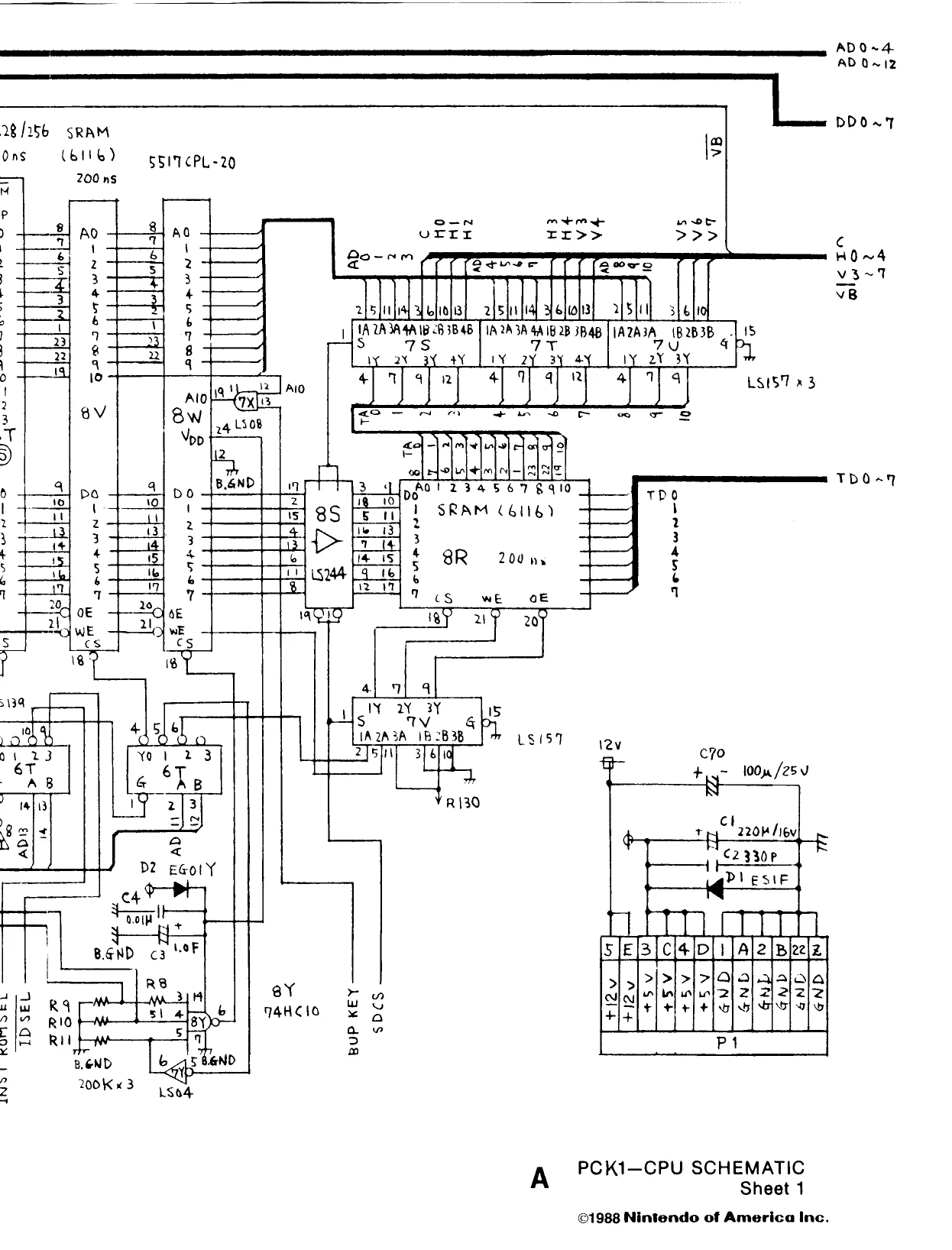
This page is a drawing, shown as the original scan.
This page reads as a drawing: its text was drawn rather than typeset, and comes out in fragments. See the original scan.
[+e iifiol #16 AEC WH x
1x TC4053BP:
oY
PCK1I— B Cc CPU SCHEMATIC
©1986 Nintendo of America Inc.
P +24v [ie +24N dT
P Counter2[u -}-———__ Counter {17 SS277B x2 mye aA
=| x el ey | % = =
© CH 33 p7 lov ADQ~4
TORD
DDO~7 sDcs
INT DETECT
INPQ D4
[—} [St [ey [oy CHSelect|® | Raa RM Ikx8
DETECT CLR
This page reads as a drawing: its text was drawn rather than typeset, and comes out in fragments. See the original scan.
SYNC
MVGND
SOUND MASK
AUX ®
A uxk
im3400 gy
RTT 2.2m
‘OK /lov SOUND
3C¢ | 4abe c27 S NOH/Iev 2.2K.
U— mail MGRN
SouwD TP] Y[S@nd IPrl <NOTE>D
- LM324 = VE pin 4 pin 2» 40bb--- Tt pin ® ace
- XK 4066 pin © 43400 \4pin
D PCKI— GND +12N @ND HIV
GND +5V MRED MSYNT
CPU SCHEMATIC Sheet 4
©1988 Nintendo of America Inc.
w < x a oe Ee
LSI6SA
INPO D4
4 TRON Start [iV] 68 04 8c FZ Feame Select] 4 J} rr po | =f Buttoufi7 >} + a «salt sh Ten co 298: hiov 5.1K
LS368A
4TH/t6N
6332
- 6 #Ty)ie LS36BA
Lsod xg BK Fpon. 8 QO +
$2 DO~4
INPO D4
NML
SPECIAL
GAME STOP
GAME RES
INT DETECT
DETECT CLR
E PCK1—CPU SCHEMATIC Sheet 5 ©1988 Nintendo of America Inc.
ya on + mle [a
| oOo « | -|2 | ° | |||
| y | ys | a | | 5 | 2 | le |e Bz | |
| e | z2 | 2 |% | a | a | z1olS a |
R
al — 4 R42 L_. 55 40) Zz 2 lok 1s347A| 'H ey] water 1[e< bons err rN “15 af a < BITRE @ loll. 2L BON-S we Badd 2 3 a“ ray
- 3H <= z z A za AB v qd alo 2rarYundon-o a 2L "<< > yt2K ram2useP-15 200s Yo°s"23 & \ ee LS 368A (Ye)
a4] = e Yi
VRAMCS efofu a ms wen tmerergT ory MAD VVUYYuvyY 2-5 _ wn A on D> nN MENASAQA RSRRARAR CLKSEATR my b22 NOOUNVTT VOVUVUVY bDooooIOH
X32: 21.47727 MHz {Ot soa Ch) 2q
RED GREEN BLUE SYNC MVGND
a a «
| eis 7 TiAl | B | a | |
| & | ohm le | w | 2 |
| BIE 2 olalg | us | Es |
ZA Ala |e
| ¥\2 < alaly | & | a |
ao Kerem oe (6116) “20005
JIN
GND ro a} jus ae
ag ad _ Or ar QeunvrHnro =~ NN Horag an- Vo GROMMODDOoOoOH vuvuuvuy FAq Oreseeraz vuy 2easa0o55
F PCK1—CPU SCHEMATIC
Sheet 6
©1988 Nintendo of America Inc.
UP44P-072A EDGE HARNESS 9P POWER HARNESS 1 DC POWER SUPPLY 2 11] —s.ue——— po 1 [etz| —creen -————
| 4 | gTz 0, | 313) —wITe ——— |
+ 8 a4
| 8 | (_ FTP ssv | LAMP ASSY |
| tal | —— | 2.| GND |
313) +12v a4
TUL] +5¥ 212) GND TTT] -WHite — [ara +12 (re) ~crar— a4 i
4P COIN HARNESS
| RON | 111] —o | —| |
| RED | 212 | ° |
ORANG! 313)
| veLuow——— [ata 1 | & | +— |
COIN COUNTER } 3P COUNTER HARNESS —
| wwrTe, onance | BROWN | i | i | THT | BROWN |
“WHITE, ORANGE + \ Reo ~ ORANGE ——— Soran BROWN —————__-_-_-__! NO ;0uN YELLO \—oreen SERVICE SW. tue ff SERVICE Sans ~ YELLOW ais
-WHITE 212 BROWN i ~ SHEL)
~ BROWN
| 15P CONTROL | cent ee chee tn ee tneeeeeeeenereeee | \ |
HARNESS = BROWN 2 RIGHT | RED 2 LEFT ORANGE 2P uP
| YELLOW | 2P_ DOWN | 1 |
GREEN GND BLUE PURPLE GAME SELECT GRAY. WHITE START BLACK GND
| L. GREEN | 2A | : | a |
| BLUE | 2B | : | |
| BLACK | Gx | : | c |
12P CONTROL HARNESS |
| BROWN | i | IP RIGHT |
| RED | raw | IP LEFT |
: ORANGE — [3734] IP up
| YELLOW | ran | IP DOWN | |
| GREEN | 515 | GND | |
| BLUE | 616 | CHANNEL SELECT | |
| PURPLE | THT | ENTER | |
| GRAY | 818 | IPA | |
| WHITE | ENE] | 7 o- | 1p 8 |
| BLACK | ia} | GND | |
| BLACK | WIL | eno |
RESET (NORMALLY CLOSED)
POWER SWITCH
| —BLU | NOISE | FUSE 5A | | | POWER CORD |
- GREEN — to riter| Le—e—o-~Co-stack - (ITT —UKITE — wale — (272 | ! | BLACK WHITE
| LAMP ASSY | (_srown | TTT] - BROWN |
WHITE 212] -WHITE > OUTPUT 1A ~~ ORANGE) 125V ‘SOUND AMP, ASSY :
| secesties | - | : | RED —] 115V |
~ 177 -waite = [1 BROWN | 105V
- (222) -Grar— [2 3 BLACK | OV + aa
(6
L eee —/| SPEAKER
| WHITE | TLL) | —waite | AC INPUT | ||
| RED | 2] | —RED | : | : | I20v |
—-~ POWER TRANSFORMER TTT] -euack — (77) \—srow — Ti 212) wie - (313) — \—re0 —— [212 GREEN ~ [212 \— orance— [313 ct YeLLoW— [41d , \—creen — [515 —arue-— [616 WON ITOR W
12P LED HARNESS | PCKI-LED P.C.B BROWN ——— [1] 1] LED p03 RED 212) LEO dz ORANGE——— [3/3] LED DDI veLLoW——— [4] 4) LEO DDO BLUE — 5{5) LED AD4 PuRPLE—— |6|6| LED ADI GRAY T{7] LED ADO WHITE —— [818] LED 10WR BLACK —— [9[9] GND BLACK —— [10 j10 | GND L.GREEN — [LLL | +5V L. BLuE—— [12 [12] +5V
WIRING DIAGRAM
SCALE: DRAWN BY: H KAMADA
DATE: 02/02/90 | APPROVED BY: MODEL: =PCK-UP
Nintendo of America Inc.
WELLS GARDNER ELECTRONICS CORPORATION cnicaco. wiinois eosse __TELEPH«
The dwawings and specifications herein are the property of WELLS~GARDNER ELECTRONICS CORP. ‘and shall not be reproduced or copied or used In whole or part as the basis for the manutacture or sale of items without written permission.
' COLOR MONITOR SCHEMATIC DIAGRAM
CONTRAST Bas
a3] te sa 5678 9 a2 RW 2N3904 |50 ore ice aie ret
vpcis97e 2221 2019 18 17 16 15.14
a|b ie OR ca Lae)
BRM oat a itz i¢ YEE $30 =| bet
aoe ay on No
+ VERT SYNC
HOR SYNC.
ono
~ VERT SYN
= nor sene |
HORIZONTS ouTPUT.
A301 Riot 220,15w 6.8K P20 Oy
DEGAUSSING com,
- RIOT ON EARLIER PRODUCTION MAY BE 1.0K. AX A480
VV COMPONENTSIVRI AVR3) ENCLOSED F-""] ARE REMOVED bisa WHEN USING P569 CONTROL BD.
| 1s 00639 | TELEPHONE: ALBANY 2-220 | 1m si. communcarion neven ro P44" | wo |
JOOX0213-O01
A 7 M1 AES bt ER hay
ALTERNATE CRT AND NECK BOARD
R305 SOOM A Vt i kal a
:
rs CUTOFF ORIVE CUTOFF DRIVE CUTOFF DRI’ te, vor
R92 um “ott oon 5
| eee | ie | F | A | |
| ee | cae | thesz tes | T | 7 |
| 7 | 1 | ! Focus | ||
| 4 | I | ‘ | sercen |
! i
csr
HORIZONTAL, ouTPUT.
us uz Size LINEARITY Og ApvusT. o17 Pa
DEFLECTION YOKE p5ca PTY FRONT CONTROL PC | oe goaRD Eleb CEO s002 | \ ' / mores : ' R304 1 ALL RESISTORS ARE IN OHMS,1/9W,5% UN- I Be Cess"oTHerwise INnoIcaTeD. i 2. CAPACITANCE VALUES LESS THAN | ARE IN MICROFARADS. ABOVE 1 IN PICOFARADS UN LESS OTHERWISE INDICATED.
- CIRCLED NUMBERS INDICATE LOCATIONS OF CERTAIN WAVEFORM READINGS,
AS CAUTION sarery carticac comvonenr,
We c-nay nsotarion nevateo component REPLACE ONLY WITH SAME TYPE PARTS AS SHOWNIN PARTS LIST.
19K7903 (Y65K7903) COMES WITHOUT CONTROL BD.
19K 7613 (Y68A7613) COMES WITH P5698 9-830 NECK BD. I9K7613 (Y70A7613) COMES WITH P569 8 9-831 NECK BD.
ZENITA COLOR MONI cmavema|D = 100X0213—0 Ol
MSD
X10
© a LEDs
ppp abcdeftg a Sees] aI
alafzielolels oom g abcdefg 16 a 3 u4 4 Ct 74Hc4s14 BEP Et ig ABCD L on lafod ‘
Pa 42] +5V + «ire Fry +5V 40] GND Er tev eseates ‘9 | GND, 8 | TORR | $ 100p| 1400p] 100p] ann § a 8 IAL 5 AD4 2 DAN4O4) 4.000 7 3 [pod 4 2 [poe 3 4 [003
1852778 X 3
| X10 | X10 | x10° | oes |
COM fy OPP , Ppt fy oP
| apcdetg | apedeta | abcdeta | ||||
| SPS PISA | Saas aI | Slaywhay =a | ||||
| : | gielsgioigis) | Oe | g[eleelnfels} | aisles) | =O | |
| apedetg [16 | apedefy |16 | apedefg [16 | ||||
| Sder | abs! | 3dr7 zaytasas Btp | 3qct | ap4_t | ||
| 7aHcass1 BIp- | 7aHC4541 | BIP— | 7ac4si1 | BIP- | ||
| le A | le _ABcO | le_AgCcO | ||||
| — | ad Hh] cu}eo} | WT | ww] |=] cu}co| | WT | wo] | feu] | WT |
anu ne im ° arvra2 © TOP VIEW
peer ee Ee by T.HIBINO foaTe SS ae a PCK-01- “LED | intend of aneries toe] |