Missile Command DP-147-2nd-01A
Missile Command (rev 3, A035467-02/04 PCBs) (Atari, 1980) · Drawing Package · 1 pages · original scan
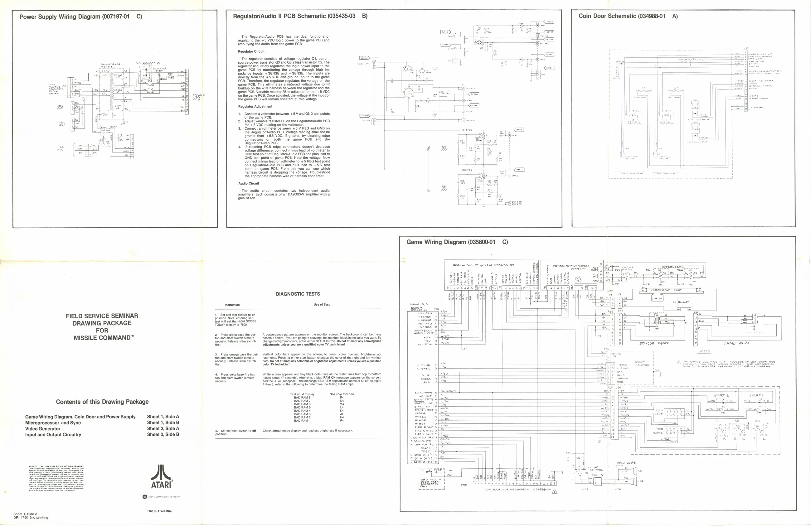
Power Supply Wiring Diagram (007197-01 C) Regulator/Audio Il PCB Schematic (035435-03
The Regulator/Audio PCB has the dual functions of regulating the +5 VDC logic power to the game PCB and amplifying the audio from the game PCB.
Regulator Circuit
The regulator consists of voltage regulator Q1, current Tianefcioa ’ ‘source power transistor Q3 and Q3's bias transistor Q2. T
SE regulator accurately regulates the logic power input to t
‘game PCB by monitoring the voltage through high im- Pedance inputs +SENSE and ~SENSE. The inputs are irectly from the +5 VDC and ground inputs to the gam PCB. Therefore, the regulator regulates the voltage on the game PCB. This eliminates a reduced voltage due to IR. Duildup on the wire harness between the regulator and the {game PCB. Variable resistor Ra is adjusted for the +5 VOC.
fon the game PCB. Once adjusted, the voltage at the input of
the game PCB will remain constant at this voltage.
Regulator Adjustment
1. Connect a voltmeter between +5 V and GND test points
(of the game PCB,
- Adjust variable resistor R& on the RegulatoriAudio PCB {for +5 VDC reading on the voltmeter.
- Connect a voltmeter between +5 V REG and GND on the Regulator/Audio PCB. Voltage reading shall not be ‘greater than +55 VOC. If greater, try cleaning edge connectors on both the game PCB and the Regulator/Audio PCB. 4, If cleaning PCB edge connectors doesn't decrease voltage difference, connect minus lead of voltmeter to ‘GND test point of Regulator/Audio PCB and plus lead to ‘GND test point of game PCB. Note the voltage. Now Connect minus lead of voltmeter to +5 REG test point ‘on Regulator/Audio PCB and plus lead to +5 V test point on game PCB. From this you can see which harness circuit is dropping the voltage. Troubleshoot the appropriate harness wire or hamess connector.
‘Audio Cireult
The audio circuit contains two independent audio amplifiers. Each consists of a TDA2O02AV amplifier with a gain often
$9) comen aueny acne ——=
23xa}| 2, 2b
24 Leh see peta DIAGNOSTIC TESTS a Le Sofelefalala ; meen
- Set sates steht 00 | i
| FIELD SERVICE SEMINAR | 1, get enn | ant | to | n |
DRAWING PACKAGE Rats 3
FOR ne 5 2 Press alpha base re bt convergence pata appears onthe monitor sceen. Te background can
| MISSILE COMMAND™ | {onand | slot owich sults, | posse color you are pong to comerge tw mont lackrs the coor you want. To | 7 |
| nous lesa slam swtan | Exange backgroun col, pros sa START ton. Dono atompl my eomergence | 4 | ||
| tise | fuses unees you se 8 qalied colo 1 tcincan | 5 | TRIAD ETA | |
| 4. Pres omega bse | but | Vora colar Bar appear on the screen, to permit color ue and bghiness a |
{on anddam autehsimcte.jatmene, Pressing el stan baton changes the clr a height and vera) ously oleae som switch Sara Be not temp ny coor hue or bghinessajustent ness you area quliod Oe feat ctor TV foci soso nin, sopngnans com 228, oe
44 Press dota base tre but- Wht screen appears, and tiny back dts race lhe ase nes rm op o btm {on and atm wich smut has abou 4 aacond) Ari, a ue RAM OK mensag appear onthe Sco, ously Stctne + wl appar he message BAD RAM appears and son i ofthe its Tw tear toh ooning to detrane to ting RAM cps
| Touro. 4 gap | 21d ci locaton | i | e | |||
| Contents of this Drawing Package | BAD RAM? | Ne | Nl | aR | ||
| BAD RAMs | ra | reer ma | == | |||
| Game Wiring Diagram, Coin Door and Power Supply | Sheet 1, Side A | BaD RAM 2 | it | Vrecx | fe | nan |
| Microprocessor and Sync | Sheet 1, Side B | moral | me | rane | [a | eT |
| Video Generator | Sheet 2, Side A | Fae Raterle | ae | |||
| 7 | 5 Set satiest swt to off | Check tact mode daly and reasust ightess It necessary | far | cmeila |
Input and Output Circuitry Sheet 2, Side B postion fs St)
cco enn) |u|
Euros) [>
Ske eee ny
| (ekol SD Sahaaln nel tober Suave any | 1 | = | KINFY | 3" |
| thn Sie erat | i | es | GON D00R WIRING BAGRAM | 034980-01 /\ |
Qe cmecnien concn
a tie © ATARING DP-147.01 2nd printing