Star Guards Upright 3 Player (0E89-00300-0000)
Star Guards (Bally Midway, 1987) · Manual · 65 pages · 32 sections · original scan
STAR GUARDS U.R.
3 PLAYER
Cially MIDWAY MFG.CO.
10601 W. Belmont Avenue Franklin Park, Illinois 60131 U.S.A. bid
Phone: (312) 451-9200 Cable Address: MIDCO Telex No.: 72-1596
OE89-00300-0000
STAR GUARDS U.R. - 3 PLAYER
TABLE OF CONTENTS
SECTION 1 - SYSTEM INFORMATION Game Description ..... aa Twas Tae 150g eee KS Oe SHS Soo Bae orgs ona. General Instructions: Installation, Servicing, & Self-Test Option Switch Settings ...........4- P.C. Board Reference Drawing .. Trouble Shooting Procedure ........
SECTION 2 - ILLUSTRATED PARTS BREAKDOWN Star Guards Front View: Picture .. Star Guards Front View: Parts List
Star Guards Rear Access: Parts List .... Header Fluorescent Light Assy.: Picture Joystick Assembly: Illustrated Parts ........ccceecccceeeee Coin Door (w/Cable) Front View: Picture ..... Coin Door (w/Cable) Rear View: Picture ... Coin Door (w/Cable): Parts List .......... Power Chassis: Picture ....... Power Chassis: Parts List ..........
SECTION 3 - COMPONENT LAYOUTS, SCHEMATICS & WIRING DIAGRAM Monitor Oscilloscope Waveform Patterns & Troubleshooting Chart ............ Monitor Schematic Monitor Theory of Operation Monitor Parts List ........... Mono Board - Component Layout Mono Board - Parts List ... Mono Board - Schematic .. Sounds Good P.C.B. - Comp Sounds Good P.C.B. - Parts List ..... Sounds Good - Schematic Dual Power Amp P.C.8. - Component Layout & Parts ‘List see Dual Power Amp P.C.B. - Schematic .....ccce cece eee e cece nue Switching Power Supply P.C.B. - Schematic .. . Uni-Power Supply Chassis Assy. - Schematic ......... tase ose eee F.C.C. Filter Bd. - Component Layout & Parts List ......... . ee F.C.C. Filter Bd. - Schematic ... ccs. cee eee eee e eee Cabinet Wiring Diagram .......... cece eee eee eee 20a eetcuesues err oe 8 to 4 Multiplexer Bd. - Component Layout, Parts List & Schematic ......... 3-36 Eprom List ..... cece eee e cece cece e eens bee e ee eeeeee a sewegeese Inside Back Cover
GENERAL INSTRUCTIONS
FOR
STAR GUARDS - 3 PLAYER - ULR. Pe eS ATER ~- ULRL
INSTALLATION
- Remove keys from the taped coin return slot and unlock to Open the coin box door.
- Remove four (4) “CABINET LEVELING LEGS" from inside the coin box.
- Tip the cabinet to the side and remove the shipping cleats from its bottom. ° Locate the threaded holes - one in each corner - and install the “CABINET LEVELING LEGS" in them. ° Level the cabinet. = When finished, the cabinet should be stable in the upright position. 4, ° Unlock and remove the rear access door to gain access to the 3-pronged line cord. Reinstall the rear access door.
- Connect the 3-pronged line cord to a 3-slot A.C. wall outlet to insure proper grounding.
- The power ON/OFF switch is located on top to the right rear of the cabinet as you face the cabinet.
TO SERVICE THE CONTROL PANEL
oo 00 0
eo eo Turn power to the game off. The control panel is held in place by two (2) latch clamps which provide constant pressure on the strikes. : They can be reached through the coin door. To release the clamps, lift up and toward the center of the control panel. Once they are released, unhook them from their strikes. Swing out the controi panel on it's hinge for servicing. To resecure the control panel, reverse this procedure.
To remove the control panel for bench-servicing only:
With the control panel in it's open position, disconnect it from it's cabling. Remove the screws which secure the continuous hinge to the cabinet. The control panel is now loose and may be bench serviced. To reinstall the control panel, reverse this procedure.
REMOVAL OF THE VIEWING GLASS
Turn power to the game off and swing open the hinged control panel. This frees the viewing glass so it can be removed.
1-3
REMOVAL
REMOVAL
REMOVAL By putting your fingers in the slot in the middle of the main-display-glass support, the viewing glass can be removed as follows:
- Lift the glass up.
- Swing the bottom edge of the glass out slightly forward.
- Drop the glass down so that its' top edge is slightly below the bottom edge of the speaker grille.
- Now, holding the glass by its' top edge and bottom edge, lift up and out. To reinstall the viewing glass, reverse this procedure.
OF THE HEADER (ATTRACT) GLASS
Turn the power to the game off. The glass is held in place by the speaker grille at the bottom and a retaining bracket at the top. The retaining bracket is secured to the cabinet top by five tamper-resistant screws. Remove these screws by using a special wrench provided in the Hardware and Bag Assembly. Remove the retaining bracket and slide the header glass up. This exposes the fluorescent light assembly. The fluorescent light tube may be replaced at this time.
- WARNING: If you drop a fluorescent tube and it breaks, IT WILL IMPLODE! Use care in handling. To reinstall the header glass, reverse this procedure.
OF THE FLUORESCENT LIGHT ASSEMBLY
Be sure the power to the game has been turned off. Disconnect it from it's power cable. . Remove the fluorescent light assembly's three mounting screws and then remove: the assembly from the cabinet. To reinstall the fluorescent light assembly, reverse this procedure.
OF THE SPEAKER(S)
Be sure the power to the game has been turned off. Remove the header glass and disconnect cabling from the speaker(s).
VOLUME CONTROL POT / OPTION SWITCH LOCATIONS
The volume control pot is located, along with the credit switch and the self-test switch, just inside the cabinet on the right side of the coin door frame. The option switch is located as shown in the attached p.c. board reference drawing. For adjustment, it can be reached
To make
To make through the game's rear access door.
the sounds louder, turn the volume pot clockwise as you face it.
the sounds less loud, turn the volume pot counterclockwise as you face it.
1-4
SELF-TEST MODE
The Self-Test mode is a special mode for checking the game switches and computer functions. It is the most complete way of checking for proper game operation and is quite easy to use.
The Self-Test mode may be entered at any time and from any mode of Operation. Simply locate the black slide switch inside the coin door and slide it to the Self-Test position. With this switch in the Self-Test postion, activate the slam switch located on the Coin Door. The game will enter the Self-Test mode immediately and display the following test menu....
- INPUT TEST
- OUTPUT TEST
- DIPSWITCH OPTIONS
- SELF-DIAGNOSTICS
- GRID TEST
TO MOVE CURSOR UP, MOVE ANY JOYSTICK UP. TO MOVE CURSOR DOWN, MOVE ANY JOYSTICK DOWN. To EXECUTE TEST, PRESS ANY START BUTTON.
- INPUT TEST: This test is designed to confirm the operation of player input switches and device switches in the game. When you enter the test, the screen displays the following:
COIN CHUTE 1 .. + OPEN PLAYER 2 BUTTON ........... COIN CHUTE 2 .. « OPEN LEFT JOYSTICK 2 ... . COIN CHUTE 3 .. + OPEN RIGHT JOYSTICK 2 .........005 CREDIT BUTTON ............ OPEN
PLAYER 1 BUTTON ......seee0e OPEN PLAYER 3 BUTTON .. LEFT JOYSTICK 1 .. veee L111 * LEFT JOYSTICK 3. ll. * RIGHT JOYSTICK 1 .........40. 1111 * RIGHT JOYSTICK 3 ........00.. A *
- All joystick switches are open: 1 = Open Switch & 0 = Closed Switch.
When you activate any one ot the above switches, its' respective message "OPEN" charges to "CLOSED" except for LEFT JC*sTICK 1 (2 and 3) and RIGHT JOYSTICK 1 (2 and 3). For :ay one of these six:
JOYSTICK POSITION SW! CH DISPLAY JOYSTICK POSITION SWITCH DISPLAY UP TITO UPPER LEFT DIAGONAL TOIO DOWN 1101 UPPER RIGHT DIAGONAL 0110 LEFT 1011 LOWER LEFT DIAGONAL 1001 RIGHT 0111 LOWER RIGHT DIAGONAL 0101
To exit this test, activate the coin door slam switch.
- OUTPUT TEST: This test is designed to confirm the operation of all 3 players’ Start button lights. These lights will flash in sequence with the following messages displayed on the screen:
START BUTTON 1 LIGHT ON START BUTTON 1 LIGHT OFF
START BUTTON 2 LIGHT ON START BUTTON 2 LIGHT OFF
START BUTTON 3 LIGHT ON START BUTTON 3 LIGHT OFF
1-5
SELF-TEST MODE, Cont'd.
This cycle continues unless:
A. You press any one of the Start buttons to hold a light ON. B. You exit the test by activating the coin door slam switch.
- DIP SWITCH OPTIONS: A11 game options such as “energy units/coin" and “difficulty levels" are adjusted through the use of dip-switches located on the Monoboard. When this test is selected, a full display of the current dip-switch settings will appear on the screen (see “Option Switch Settings" on page 1-7). To exit this test, activate the
- coin door slam switch. .
- SELF-DIAGNOSTIC TEST: This test is designed to effectively locate and identify any malfunction of the on-board computer. when selected, the game enters this mode immediately and begins scanning the memory stored in rom and ram. If the test is successful, at the end of the scan "ALL TEST OK" is displayed on the screen. If a defective component is found during the scan, that component and its' location will be displayed on the screen. The entire test is performed approximately in 15 seconds. To exit the test, activate the coin door slam switch.
- GRID DISPLAY: This test is designed to display a crosshatch pattern used in adjusting the color monitor. This pattern may be used to adjust convergence, color balance, vertical linearity, and vertical/horizontal size. To exit this test, activate the coin door slam switch.
POWER-UP TEST MODE
This test sequence is designed to effectively locate and identify any malfunction of the Sounds Good p.c. board. Te. results are indicated by an L.E.D. located on the sound board.
On power-up under normal ope-ation, the sound board runs through its' self-diagnostic checks flashing its' L.E.D. to anncunce every successful test. At the end of the test run, the attract mode begins.
If one of the tests fails however, the L.E.D. will not flash for the failed test no- for any remaining tests in the sequencial run. At this point, “SOUND BOARD INTERFACE ERROR appears on the screen.
The following is the Self-Test routine for the Sounds Good Board:
lst FLASH - Determines if the ROM (U7) is good. 2nd FLASH - Determines if the ROM (U8) is good. 3rd FLASH - Determines if the ROM (U17) is good. 4th FLASH - Determines if the ROM (U18) is good. 5th FLASH - Checks to see if the RAM (U6, U16) is good. 6th FLASH - Checks the PIA (6821) (U9).
1-6
STAR GUAROS U.R.
OPTION SWITCH SETTINGS
LILTTTTTATITATIT LATTE SWITCH NO. 2 - AT AL3 - LOCATED ON MONOBOARD //////////////(11/ 11/1
ENERGY UNITS/COIN 8 ENERGY UNITS/COIN 10 ENERGY UNITS/COIN 12 ENERGY UNITS/COIN 14 ENERGY UNITS/COIN
ATTRACT Seon SOUNDS: NO SOUNDS
DIFFICULTY LEVEL: EASY MEOIUM HARDER HARDEST
WIDEO FREEZE MODE:
—“WORMAL VIDEO FREEZE VIDEO SWFL SW#2 SW#3 SWH4 SWH5 SW#6 SWH7 SWH8 SW#O SW#1O WOT «NOT WOT NOT USED USED
FACTORY SETTING - ALL LOGIC SWITCHES SET IN THE "OFF" POSITION | PART NO. MO51-00E89-A007
1-7
PC. BOARD REFERENCE DRAWING
FOR _MONOROARD SYSTEM
MONOBOARD AN84-91787-ABB9
TION SWITCH "21 (10-PASI TION)
Orr
INTRODUCTION
This manual offers generalized troubleshooting procedures for common types of malfunctions which can be applied to most video games. We will not attempt to give you specific instructions for troubleshooting particular games because this would involve hundreds of pages of more repetitive instructions, differing only in the specific details of each game.
The most common problems occur in harness components such as the coin acceptor, player controls, interconnecting wiring, etc. These areas are covered in moderate detail.
The TV Monitor and Game Logic Printed Circuit Boards (PCB's) provide their fair share of problems too, but not to the extent of the harness and its component parts.
As you already know, the Game Logic PC Boards are complex devices. Each contains a great number of different interrelated circuits. The major changes which give each game its own particular individuality are accomplished in the EPROMS and other Integrated Circuit devices that are installed on each of these PC Boards.
GENERAL TROUBLE SHOOTING SUGGESTIONS
The first step in troubleshooting is to correctly identify the malfunctions symptoms. This includes not only the circuits or features malfunctioning, but also those still operational. A carefully trained eye will pick up other clues to what's wrong as well. For instance, a game in which the computer functions fail completely just after money was collected may have a quarter shorting the PCB traces. Often an experienced troubleshooter will be able to spot the cause of a problem even before opening the cabinet.
After all the clues are carefully considered, the possible malfunctioning areas can be narrowed down to one or two good suspects. Those areas can be examined by a process of elimination until the cause of the malfunction is discovered.
HARNESS COMPONENT TROUBLESHOOTING
Typical problems falling in this category are coin and credit problems, power problems, and failure of individual features.
NO GAME CREDIT - - For example, a prospective game player inserts a quarter or token and is not awarded a game. The first thing to check is whether or not the quarter or token is returned. If it was returned, the malfunction most certainly lies in the coin acceptor itself. First, use a set of test coins (both old and new) to ascertain that the player's coin is not undersize or underweight. If your test coins are also returned, coin acceptor servicing is indicated. Generally, the cause of this particular problem is a maladjusted magnet gate. Normally, this will mean slightly closing the magnet gate by turning the adjusting screw out a bit.
1-9
If the quarter or token is not returned and there is no game credit, the cause of the malfunction may be in one of several areas. First, try operating the coin return button; if the coin is returned, the problem is most likely in the magnet gate. Enlarge the gap according the coin acceptor manufacturers service procedures. If this does not cure the problem, remove the coin acceptor, clean it, and perform the manufacturers suggested major adjustment procedure.
If the trapped coin is not returned when the wiper lever is actuated, you may have an acceptor jammed by a slug, gummed up with beer, a jammed coin chute, or mechanical failure of the acceptor mechanism. In this case, first check for the slug that will generally be trapped against the magnet. If a slug is found, simply remove it and test the acceptor. If the chute is blocked, remove the acceptor and remove the jammed coins. If there is actual failure of the acceptor, remove the unit and repair as indicated by the acceptor manufacturers service procedures.
If the coin is making its way through the acceptor (that is, falling into the coin box), yet there is still no game credit, you either have a mechanical failure of the coin switch or electrical failure of the coin and credit circuits. The first place to begin is by checking the coin switch. Most of these switches are the make/break variety of micro switch. They are checked for continuity between the “NO", "NC", and "C" terminals. When not actuated, the "NC" and "C" terminals should be continuous and the "NO" terminal open. When actuated, the “NO" and “C" terminals should be continuous and the "NC" terminal open. If the coin switch checks good, inspect the solder connections to the coin switch terminals to be sure there is good contact at this point. If necessary, use a continuity tester and check from the terminal lug on the switch to the associated PCB trace. This will tell you if there is a continuous line all the way to the credit circuit.
If the coin switch wires do check good, the problem is in one of the game logic boards - most likely in the coin and credit circuitry.
If you do get a game credit when a coin is deposited, but the game will not start when the one or two player start button is pressed, there may be a problem in the start switch, the interconnecting wiring, or the game logic boards. First, check the switch. If the switch is OK, proceed to check the wiring. Again, make sure you go from the terminal lug on the switch to the PCB trace. This way, you will check the terminal contact as well as the PCB edge connector contact. If the wiring is continuous, proceed to check the PCB credit circuit. If not, check each section of the wiring, until the discontinuity is located. If the wiring is OK, the problem must lie in the games logic boards.
TRANSFORMER AND LINE VOLTAGE PROBLEMS
Your game MUST have the correct line voltage to operate properly. If the line voltage drops too low, one of the games logic circuits will disable the credit acceptance circuit. The point at which the games logic circuits will fail to function is approximately 105 volts AC.
Low line voltage may have many causes. Line voltage normally fluctuates a certain amount during the day as the total usage varies. Peak usage times occur mainly at dawn and/or dusk. So if your games problem seems to be related to the time of day, this may be a factor. A large load connected to the same line as the game (such as a large air conditioner or other device with an exceptionally large electric motor) may drop the line voltage significantly when starting up. This drop can result in an intermittent credit problem. In addition, poor connections in the location wiring, plug, or line cord may also cause a significant drop in power. Cold solder joints in the games harness, especially in areas like the transformer connections, interlock switch, or fuse block, may also produce the same results, although probably on a more permanent basis.
- Sometimes location owners (especially in bars) replace light switches with dimmer rheostats, and the game is sometimes on the same line. Obviously, the voltage available to the game is going to drop dramatically when the dimmer is turned down.
In any case, the way to check for proper line voltage is with your VOM. Set the VOM to the 250 VAC scale and stick the probes into the wall outlet the game was connected to. If it's OK here, check the transformer primary connections. If you do not get 117 VAC, examine the solder joints on the transformer, fuse block, and interlock switch. If you do get 117 VAC, the problem must be either in the transformer, harness connections, or in the PCB power supply.
If you suspect the transformer, check its secondaries with the VOM set to the 50 VAC scale and correlate the readings with the legend on the side of the transformer. The transformer must also be correctly grounded, so check the ground potential as well, especially if there is a hum bar rolling up or down the Monitor screen.
NO POWER, NO PICTURE - - If the Monitor screen is completely dark, first look in back of the Monitor to see if the CRT filament is glowing. If it is, try adjusting the brightness control. If no luck here, put your ear near the Monitor and listen for the high-pitched B+ hum produced by the flyback transformer. If you get the hum but no picture, and you have tried adjusting the brightness, major Monitor servicing is indicated. ”
If the monitor seems completely dead, check the rest of the game to see if it has power. If it doesn't, go directly to the wall outlet and check there. If OK there, check the game fuse(s), interlock switch, and interconnecting wire lengths.
Sometimes it is difficult to tell if a slow-blow fuse has blown. If in doubt, check it using any of the VOM "R" scales.
HARNESS PROBLEMS - - Other harness problems include blowing fuses and malfunctioning controls. The repeating blown-fuse problem can sometimes be quite exasperating to solve. Short circuits have the tendency to occur in areas almost impossible to find. First, try inserting a new fuse as old fuses age and sometimes blow without cause. If the new fuse also blows, you definitely have a short.
The best way to approach this problem is by disconnecting devices that may be causing the problem, such as the TV Monitor, the various PCB's one at a time, and the isolation transformer. Disconnect the devices by FIRST turning the game_off, disconnecting it from its wall outlet. Remove the blown fuse and connect your VOM across the terminals of the fuse block (this will save blowing a fuse each time you want to check the circuit). Set your VOM to one of its resistance scales. You should be reading a short. If not you probubly have a part that only shorts out after it is heated up - we'll cover this in a minute. So, assuming you are reading a short on your VOM, disconnect the components from their cabling one at a time, checking the VOM after each one is disconnected. When the short disappears, you have just disconnected the bad component. If all components are disconnected and the short still remains, the problem is in the harness and only patient exploration will reveal its location. Carefully examine all the wiring, looking for terminals that may be touching, metal objects such as coins shorting the connections, or burned insulation. If necessary, use the VOM to check each suspected wire.
OK, now lets assume that you connected your VOM across the fuse block terminals as stated above and you did not read a short. This most likely means that you have a component somewhere in that game that ONLY goes bad AFTER it heats up. It checks good when its cold. In this case, turn the game off and disconnect ALL of its components. Install a known good fuse in the fuse block. And turn the game on. If the fuse does not blow after a few minutes, you know that it is not anything to do with the wire harness. (In this instance, it shouldn't be, actually. But it never hurts to check.) Next, turn the game off again and reconnect ONE component. Turn the game back on and wait a few minutes to see if the fuse blows. If it does not, turn the game off again and reconnect another single component.
Turn the game back on and wait a few minutes to see if the fuse blows. Repeat this procedure until the fuse blows. When it does blow, the last component you connected has the part on it that is going bad after it warms up and is shorting out.
MALFUNCTIONING CONTROLS - - The most common problem here is the bad potentiometer (pot). Typically, a bad pot will cause the image on the screen to jump when it reaches a certain point. The only cure for this one is to install a new pot.
If a feature that is operated by a switch (for example, joysticks, foot pedals, control panel buttons) does not operate at all, check the switch with a VOM or continuity tester to verify its operation. If the switch does not check good, replace it. If the switch is OK, you should suspect the input to the switch from the PCB. In this case, get out the harness and logic schematics and check to see what kind of input is supposed to be at this switch. In many cases, the input will be +5 volts DC. If so, use the VOM to check its presence with the game turned on. Normally, the switch is used to pull a +5 volt DC line LOW to GROUND or to pull a LOW line HIGH. If the PCB output is missing, check the wire length from the PCB. If you find the signal at the PCB trace, the wire length or connection is at fault. If there is no signal at the PCB trace, begin exploring the PCB using the logic schematics and game manual.
SECTION 2
ILLUSTRATED PARTS BREAKDOWN
STAR GUARDS U.R. - 3 PLAYER ~ FRONT VIEW
STAR GUARDS U.R. - 3 PLAYER - FRONT PARTS LIST ORDER BY PART NUMBER ONLY
er a ea [= i fe ene wa [= an [ve TT PTT T-T [i me a ETT | 4 | OE36-00102-O00XF | SPEAKER GRILLE = i i Fe weno TT O.T COT eT [eine sr ome nae
0E89-00901-00XF jMAIN VIEWING GLASS
0017-00003-0465 |WELLS-GARDNER - 19" COLOR DUAL SYNCH HORIZONTAL MTG. MONITOR
AE68-00004-0000 |CONTROL SHELF ASSY.: (INCLUDES ITEMS 20 THRU 31)
0017-00009-0534 |BASSICK CLAMP (2 REQ'D.) (NOT SHOWN)
-0555-00901-0000 |PIN: LOCATING (MOLDED) (8 REQ'D.) (NOT SHOWN)
11 0090-00002-04BK |COIN DOOR FRAME: LARGE BLACK, TRIPLE
A982-00014-0021 12 U.S.A. 25¢ COIN DOOR & CABLE ASSY.
CASH BOX: MOLDED (BEHIND COIN DOOR) 13 0017-00009-0477
0950-00115-0000 }COVER: COIN BOX (BEHIND COIN DOOR) +. 0950-00901-0000 |BASKET: COIN BOX - WIRE (BEHIND COIN DOOR)
0017-00102-0048 |LEG LEVELERS (4 REQ'D.)
0017-00103-0026 |NUT 3/8 -16 HEX (FOR LEG LEVELERS) (4 REQ'D.)
0935-00906-1100 |PLATE: KICK L = 27 - 5/8"
19 0E36-00105-0100 }BRKT.: SHELF-SUPPORT: RIGHT (UNDER CONTROL SHELF)
BRKT.: SHELF-SUPPORT: LEFT (UNDER CONTROL SHELF) 0E 36-00105-0200 im L. NOT PART OF ABOVE ASSEMBLY & MUST BE ORDERED SEPARATELY
2-3
STAR GUARDS U-R. - 3 PLAYER - FRONT PARTS LIST, CONT'D.
ORDER BY PART NUMBER ONLY
PART NO. DESCRIPTION
Ea AE36-00010-O0XF |CONTROL - APRON WELD ASSY. AEB9-00005-0000 CONTROL SHELF CABLE ASSY. (UNDER CONTROL SHELF)
23 AE36-00021-0000 [JOYSTICK - ASSY.: SHAFT & PLATE (6 REQ‘'D.) (SEE PAGE 2-10) OR
0017-00009-0694 {JOYSTICK - ASSY.: SHAFT, BALL & PLATE
Em QE89-00100-O0XF |PLATE: CONTROL SHELF 0£89-00902-O0XF ]OVERLAY: CONTROL-SHELF
26 | 0017-00032-0093 |SWITCH: SPST PUSHBUTTON W/RED LIGHT (3 REQ'D.) 0£36-00106-0000 |STRIKE: CONTROL-SHELF (2 REQ'D.) (UNDER CONTROL SHELF)
El 0£89-00501-0000 {CONTROL SHELF: WOOD 0017-00101-0138 |¥#8 X 5/8" TORX TAMPER RESISTANT PAN SCREW (8 REQ‘'D.)
0017-00101-0620 |8-32 X 1/2" CARRIAGE BOLT (24 REQ'D.)
NUT: 8-32 HEX W/SEMS (28 REQ'D.) 0017-00103-0061
2-4
STAR GUARDS U.R. - 3 PLAYER —- REAR ACCESS
STAR GUARDS U.R. - 3 PLAYER - REAR ACCESS
STAR GUARDS U.R. - 3 PLAYER - REAR ACCESS PARTS LIST
ORDER BY PART NUMBER ONLY
ITEM PART NO. DESCRIPTION ‘A945-00062-0000 ON-OFF SWITCH & PLATE ASSY.
| | 0017-00032-0105 | SWITCH: 2PST 6 AMP
ix}
AE89-00012-0000 |CARDRACK W/MONOBOARD ASSY. (SEE PG. 2-5)
BO84-91787-AE89 |PROGRAMMED MONOBOARD ASSY.
AE36-00013-0000 | SHIELD & SPACER ASSY.: MONOBOARD
AE68-00006-0000 |MASTER CABLE W/BRKT. ASSY.
A515-00021-0000 |MULTIFUNCTION SWITCH BRKT. ASSY. (INCLUDES FOLLOWING 6 ITEMS)
(0017-00032-0007 |SWITCH: SPDT SLIDE 4 AMP ee CREDIT: TEST-SWITCH: VOLUME |
0017-00032-0051 |BUTTON: SHITCH, RED ~ | 105€-00001-0017 |POT.: O-1K CBN 1/2W 0017-00103-0075 NUT: 3/@ - 32 HEX 7
0017-00104-0104 |WASHER: .375" I.D., .562" 0.D., .018 TH. INTERNAL TOOTH LOCK L AE36-00008-0000 |HIGH VOLTAGE CABLE ASSY.
0017-00003-0500 |LINE-CORD: 3-CONDUCTOR 18 AWG.
AE36-00002-0000 |VIDEO CABLE ASSY.
SIAR GUARDS U.R. - 3 PLAYER - REAR ACCESS PARTS LIST (CONT‘D.)
ORDER BY PART NUMBER ONLY
B
A945-00059-0200 |POWER CHASSIS: 130VA - SWITCHING (SEE PG. 2-17)
CABINET ASSY.
] 9£68-00500-0000 [CABINET 3 | 4961-00007-0000 |CASTER-WHEEL ASSY. (INCLUDES FOLLOWING 4 ITEMS) (2 REQ'D.) 0017-00042-0255 |CASTER WHEEL
WHEEL BRKT.
LAMP CONTROL P.C. BOARD ASSY.
0E36~00102-OOXF |MONITOR RAIL (2 REQ'D.) (BEHIND REAR WALL OF CABINET) ay
(INCLUDES ITEMS 12 & 13)
ray nN
~ a oF BO84-91787-AE89 |8 TO 4 MULTIPLEX BD. ASSY. L FCC ~ FILTER BD. ASSY.: MONOBOARD N B084-91870-A000
‘0311-00100-0000 }BEZEL MOUNTING BRKT. (2 REQ'D.) (BEHIND REAR WALL OF CABINET) L ADDITIONAL PARTS LiST
0£89-00300-0000 |CATALOG: STAR GUARDS U.R. - 3 PLAYER
MO51-00E89-A007 {TAG: OPTION SWITCH SETTINGS |
AE36-00009-0000 }REAR DOOR ASSY. (INCLUDES FOLLOWING 6 ITEMS) |
0£36-00502-0000 |REAR DOOR (WOOD)
—T : 0017-00005-0050 |DOOR LOCK W/2 INDIVIDUAL KEYS
0017-00005-0209 |LOCK PLATE (SCREW MTD.)
0017-00009-0490 |VENT GRILLE - 5-5/8 SQ. IN. (2 REQ'D.) | PERFORATED VENT GRILLE (2 REQ'O.) 0618-00117-O0XF
0639-00116-O0XF |CAM: OFFSET 30 DEGREES
2-8
MICAUCK TLUUKESLENT LIGHT ASSY.-PARTS LIST PART NO. A595-00011-0000 TOO ORDER BY PART NUMBER ONLY |
DESCRIPTION
FLUORESCENT BRKT.
18" COOL WHITE FLUORESCENT LAMP
LAMP LOCKS (2 REQ'D.)
FLUORESCENT SOCKET (2 REQ'D.)
0017-00003-0412 FLUORESCENT STARTER HOLDER W/LEADS
#6-32 X 1/2 PHIL. RND. HD. M.S. (4 REQ'D.) | __ fee 00101-0347 0017-00003-0019 {FLUORESCENT STARTER
0017-00003-0026 | BALLAST
#8-32 X 5/16 SLT. HEX HD. SCR. (4 REQ‘D.) me 00101-0598
JOYSTICK ASSY. SHAFT & PLATE PART NO. AE36-0002 1-0000
Reversible Ball Handie a Aetivator
Safety Chamber
Safety Chamber ‘Satety Chamber
Recess Recess
Steet Collar
Stee! Shaft
Batt Bearing -
Spring ———
Surtace for 8-Way cio Reversible Joystick \ Actwator
Surtace for 4-Way Joystick
Salety Chamber
Electronic 4/8-Way Joystick Assembly
Shaft w Ball (Bally Sente Part No. 0017-00009-0645)
Plate w Switches (Bally Sente Part No 091/-00009-0686)
COIN DOOR W/CABLE: BLACK 3-CHUTE PART NO. A982-00014-0021
FRONT VIEW
3® NOT SHOWN
COIN DOOR W/CABLE: BLACK 3-CHUTE PART NO. A982-000 14-0021
iw, @ @®
@ @ @ @ @ @ @ @ TOP VIEW
BOTTOM VIEW % NOT SHOWN
COIN DOOR W/CABLE: BLACK 3~CHUTE - PARTS LIST, CONT'D. PART NO. A982-00014-0021 ORDER FROM COIN MECHANISM BY PART NUMBER ONLY (312) 279-9150
DESCRIPTION
0017-00005-0003 |COIN ACCEPTOR W/STRING CUTTER (3 REQ'D.) OR n a
4-40 HEX NUT (6 REQ'D.) | 8000-10 mec. MTG. BRACKET "STAKED" (3 REQ'D.) 8000-18 SW. CHUTE (SMALL) (3 REQ'D.)
i
101-4-16 4-4 X 1" ROUND HEAD MACHINE SCREW (6 REQ'D.)
SWITCH COVER (3 REQ'D.)
8000-13
8800-9-1-R COIN RETURN CUP (3 REQ'D.)
SLAM SWITCH BRACKET
SLAM SWITCH
100-4-6 4-36 X 3/8 ROUND HEAD MACHINE SCREW (3 REQ'D.) [39 | 8800-24 Vial. GT. LOCK ERY WANTS 40 | x615 LOCKING CAM Ee 1 7800-7 ~~‘ (KEY HOOK 0017-00007-0019 |KEY HOOK
A090-00089-0000 |COIN METER ASSY. W/DIODE
A982-00015-0011 |COIN DOOR CABLE ASSY.
0017-00009-0609 |GROUND STRAP: L = 7" W/BLACK COVER
0017-00103-0061 |NUT: 8-32 HEX W/SEMS ST. (2 REQ'D.)
0017-00103-0084 |NUT: 6-32 HEX W/SEMS ST. (2 REQ'D.)
0017-00104-0019 |WASHER: 6 145 - .375 - 032 FLAT ST.
NOT PART OF ABOVE ASSEMBLY & MUST BE
| ORDERED SEPARATELY, THROUGH BALLY MIOWAY MFG. COQ. 2-14
COIN DOOR W/CABLE: BLACK 3~-CHUTE - PARTS LIST, CONT'D. PART NO. A982-00014-0021 ORDER FROM COIN MECHANISM BY PART NUMBER ONLY (312) 279-9150
PART NO. DESCRIPTION
0017-00005-0003 |COIN ACCEPTOR W/STRING CUTTER (3 REQ'D.) OR 26 | 0017-00005-0214 COIN ACCEPTOR W/STRING CUTTER
8000-10
8000-18 SW. CHUTE (SMALL) (3 REQ'D.)
101-4-16 4-4 X 1" ROUND HEAD MACHINE SCREW (6 REQ'D.)
8000-28 SWITCH COVER (3 REQ'D.)
COIN RETURN CUP (3 REQ'D.)
8800-9-1-R SLAM SWITCH BRACKET | 4-40 HEX NUT (6 REQ‘D.)
MECH. MTG. BRACKET “STAKED“ (3 REQ'D.)
| 37 | 7800-42 | SLAM SWITCH | |
| 38 | 100-4-6 | 4-36 X 3/8 ROUND HEAD MACHINE SCREW (3 REQ'D.) | | |
39 | 8860-24 DBL. BTD. LOCK & KEY W/NUTS | L 40 | x615 LOCKING CAM a |
| 41 | 7800-7 | KEY HOOK |
| oan ane 42 * | 0017-00007-0019 |KEY HOOK 43 * | A090-00089-0000 |COIN METER ASSY. W/DIODE | 44 A982-00015-0011 |COIN DOOR CABLE ASSY.
0017-00009-0609 |GROUND STRAP: L = 7" W/BLACK COVER
0017-00103-0061 |NUT: 8-32 HEX W/SEMS ST. (2 REQ'D.)
47 * | 0017-00103-0084 |NUT: 6-32 HEX W/SEMS ST. (2 REQ'D.) 48 * | 0017-00104-0019 |WASHER: 6 145 - .375 - 032 FLAT ST.
- hot PART OF ABOVE ASSEMBLY & MUST BE
ORDERED SEPARATELY, THROUGH BALLY MIDWAY MFG. CO.
2-14
POWER CHASSIS: 130VA (SWITCHING) PART NO. A945-00059-0200
9.18)
POWER CHASSIS: 130VA (SWITCHING) PARTS LIST PART NO. A945-00059-0200
ORDER BY PART NUMBER ONLY
ITEM PART NO. DESCRIPTION A945-00057-D1XF =| CHASSIS SUB-ASSEMBLY
0945-00117-O1XF |POWER SUPPLY COVER
3 0017-00101-0123 {8 X 4 UNSLOT HEX HD. SCREW (8 REQ'D.)
0 joo17-00003-0114 [LINE FILTER - 5 AMP, 115VAC (NOT SHOWN) 1 jo017-0o101-0067 | X 6 PHL. PAN HD. (2 REQ'D) 2 }o017-00003-0433 | |Fuse HOLDER 0017-00003-0263 {FUSE MDA, 3AG, 4 AMP, 115 VAC Ga
A945-00030-0600 |CONNECTOR & CABLE ASSEMBLY
0017-00021-0370 |TERMINAL STRIP
0017-00101-0140 4-40 X 5 PHL. PAN HD. SCREW (2 REQ'D) ele Pl w
0017-00009-0580 |CAPACITOR ALIGNMENT TOOL
8 0945-00912-0000 |{ADJ. TOOL HANDLE
ADDITIONAL PARTS LIST
115E-00001-0004 ]VARISTOR-METAL OXIDE (UNDER CHASSIS)
0017-00021-1110 {2 POSITION TERMINAL BARRIER STRIP (UNDER CHASSIS)
0017-00101-0780 {6 X 8 PHIL. PAN HD. SCREW (UNDER CHASSIS)
0017-00103-0084 |6-32 HEX NUT W/SEMS (UNDER CHASSIS)
2-16
SECTION 3
COMPONENT LAYOUTS, SCHEMATICS & WIRING DIAGRAM
TYPICAL OSCILLOSCOPE WAVEFORM PATTERNS
The waveforms shown below were observed on a wide band oscilloscope. The input signal was from a crosshatch generator with a horizontal syne frequency of 15.73kHz and a vertical frequency of 60 Hz. If the waveforms are observed on an oscilloscope with a limited high frequency response, the corners of the pulses will tend to be more rounded than those shown, and the amplitude of any high frequency pulse will tend to be less.
Each photograph is numbered. These numbers correspond to the circled numbers on the schematic diagrams.
Photographs 12, 13, 14, 15 and 16 are of the red signal at various points along the red video channel. corresponding points along the green and blue video channels will look similar. The waveforms at
| 2V/DIV | 20 uSEC/DIV | 2V/DIV | 10 uSEC/OIV | OSV/DIV | 20 uSEC/DIV | O.2v/0IV | 5MSEC/DIV |
7,
| 1OV/DIV | SMSEC/DIV | 2V/DIV | 20 uSEC/OIV | 1V/DIV | 20 uSEC/DIV | OSV/DIV | 10 uSEC/DIV |
| 9. | 10. | 12. |
O.SVv/DIV 20 uSEC/OIV
| 2OV/DIV | 20 uSEC/DIV | BV/DIV | 20 uSEC/DIV | 1V/DIV | 0.2MSEC/DIV |
O.2MSEC/DIV
| 1V/DIV | O.2MSEC/DIV | 1ViDIV | 2viorv |
O.2MSEC/DIV 1violv O.2MSEC/DIV TROUBLESHOOTING CHART
NO PICTURE ‘SEE NOTE 4
CRT FILAMENT LIT
7 ves
CHECK FOR GATE PULSE ATIC! Lina
CHECK ALONG VIDEO CHANNEL FROM VIOEO INPUT AT P! TO VIDEO ‘OUTPUT TRANSISTORS (ON NECK BOARD, y y ‘CHECK FOR GATE REFER TO NO PULSE OUTPUT HIGH VOLTAGE FROM IC2, PIN 12 CHART
‘CHECK FOR OPEN. HORIZONTAL YOKE ‘cIRCUIT.
y REFER TO SYNC PROBLEMS, CHART,
SYNC PROBLEMS SEE NOTE 8
NO HOR SYNC. NO VERT. SYNC. y Y NO VERT. SYNC NO HOR. SYNC. HOR, SYNC OK VERT. SYNC OK
y ‘CHECK SYNC AMPL CKT, a7, NO HIGH VOLTAGE
B+ GREATER
THAN 130 VDC
CHECK B+ (123V) AT IC4, PING, NECK BOARD. P202, PIN 3 ‘CHECK AC INPUT.
‘CHECK FOR SHORTED | icq 8+ REGULATOR, C4, PINS 1-4 SHORTED
(40k
USING VARIAC, DECREASE AC INPUT TO ZERO. THEN SLOWLY INCREASE AC SUCH THAT B+ = 123 VDC.
MONITOR OPERATES
eu CHECK WAVEFORM IC 2, PINS 1,2,3.4 ANE LOOK FOR CAUSE OF ‘SHORTED IC4: OVERLOAD CONDITION. SHORTED Qt FOR EXAMPLE
CHECK FUSE: IF FUSE IS OPEN, CHECK FOR SHORTED HOR OUT- PUT TRANSISTOR Qi! AND SHORTED B+ REGULATOR, C4.
MONITOR STILL DOES NOT OPERATE
(CHECK WHETHER HOR. OS: RIS OPERATING. » AND (CHECK RETRACE TUNING CAPACI- TOR, C36 pm
y
EXAMPLE: C36 DECREASED IN VALUE. HV. HOLD DOWN CIRCUIT IS PREVENTING MONI- TOR OPERATION AT NORMAL AC INPUT CHECK FOR, FAULTY CONDITION CAUSING H.V. TO BE TOO HIGH
CHECK HV. HOLD DOWN, CIRCUIT. O10, 012, 1C2
VERTICAL SWEEP PROBLEMS ‘SEE NOTE 8
BRIGHT. THIN, WAVY LINE AT CENTER OF CRT. no, or very | | { cHeck ‘ LITTLE VERT 2av. vane CAL SWEEP. YOKE. suppLy | ‘CHECK’ ‘CHECK HOR SYNC. ic2 INVERTER CKT 6.
hea te2 ! ‘CHECK FOR OPEN VERT! CAL YOKE WINDINGS OR VERTICAL YOKE PATH. aa
y ‘CHECK VERTICAL | LATOR AND TRIGGER CKTS: ‘CHECK HOR 1C2, PINS 10, 11, 12 AND 13, AFC: IC2, PINS 2 AND 3 DC BLOCKING CAPACITOR 50, CHECK VERTICAL DRIVE AND FEE POSITION CKT. Q9. 7 BACK CKTS, IC2, PINS 7.8.90 8 11
TROUBLESHOOTING NOTES
- The troubleshooting chart mentions specific components to be checked. It is intended that the entire circuit associated with these components be checked.
2.This chart is a guide to servicing rather than a complete list of each component that could fail. Therefore, troubleshooting should not be limited only to those components mentioned in the chart.
- It is always useful to begin checking a circuit by measuring the DC voltages and then comparing the measurements to those listed in the Typical DC Voltages chart.
- The cutoff controls and drive controls on the neck board and the screen control at the bottom of the flyback transformer have been preset at the factory. When servicing the monitor for a lack of video, do not adjust any of these controls unless it is suspected that the problem is a result of these controls having been tampered with. Otherwise do not adjust these controls; if they are so severely out of adjustment that there is a lack of video, then there is something malfunctioning,
- The Wells-Gardner Service Department does accept telephone calls for servicing assistance. Call 1-312-252-8220, between 7:00am and 3:30pm Central Time. Ask for the Service Department. The Service Department is closed during the first two weeks of July. Telephone assistance is notavailable during this period. Before calling, be sure to have available the model number of the monitor being serviced and the schematic diagram of the monitor being serviced. Jona dimension af tha nicti
- Replacement parts may be ordered from the Service Department between 7:00am and 4:30pm Central Time.
- All monitors are equipped with automatic degaussing coils which demagnetize the picture tube every time the monitoris turned on after being off for a minimum of 20 minutes. Should any part of the chassis become magnetized it will be necessary to degauss the affected area with a manual degaussing coil. Move the coil slowly around the CRT face area and all surrounding metal parts. Then slowly withdraw for a distance of 6 feet before turning off.
- Horizontal vs. Vertical:
‘Some models have the picture tube mounted vertically rather than horizontally. That is, the picture tube is mounted in the frame such that the long dimension of the tube is up and down. Examples of this include (but are not limited to) Models 13K7851 and 197951. Other than the physical orientation of the picture tube, there is no electrical difference between these models and their horizontal counterparts. The same circuits, the vertical circuits, produce and control deflection along the short dimension of the tube in all models.
‘The same circuits, the horizontal circuits, produce and control deflection along the long dimension of the tube in all models. Therefore, wherever “vertical” appears in this manual or on the monitor, it refers to the short dimension of the picture tube; wherever “horizontal” appears, it refers to the tuba. =
K7000 COLOR MONITOR SCHEMATIC DIAGRAM
nen fi
orn |2
pou 3
no [4 VERT sync [5 sHor sync [6
No
VERT SYNC.
= HOR SYNC
r20vac 50760mz
DEGAUSSING Corl. g tev =an A
34s
1c upcise7c 019 18 716 15 @ 9 10
ark a3 RIS: 83, 23906 Hi Be cos CESS 2n3904 pre To ar os eu si CONTRAST var Tox
BRIGHTNESS RSs 1K a2 vece WA P448 ka 29.0mmNECK 7
tev
+]e
[pve 2x. (0,25v' RG! 33x SER
R301 RIO! 220,15w 6.8K eT
care caal's BEY | zo aro an Eee | Ee ited
80 esi 01 001 vm HORIZONTAL soo POstTion te ® HOR 910 [2scafaez 2 Grave A Tess Joe * 3d eT 3h, 100 RTS 33 cs 208 ci oe | ne 863 Sov | sow REG 2.2K ®
es H Ht 28, of
*R302 IS PRESENT ONLY ON 19K 7600 AND 19K7900 SE- RIES MONITORS. cas O18 HORIZONTAL
‘OUTPUT
+2av SCREEN
R93 Kw
4a 2 1MOOV PP z iD)
a es
VERTICAL VERTICAL POSITION
RIO? it
VERTICAL SIZE 50-6OHz
ALTERNATE CIRCUIT FOR LATER PRODUCTION Ros ane a4 47K
R98 22K. Roo 22kKw Ror 270,3 HOR © Pos
ut Le SIZE LINEARITY 7 ADJUST. 7 Reo
Pa
- Power Up Warning-
present a shock hazard. PARTS AS SHOWN IN PARTS LIST.
WARNINGS: ALTERNATE CRT AND NECK BOARD
13K7800 SERIES 19K7600 SERIES I9K7900 SERIES
Nores,
1 ALL RESISTORS ARE IN OHMS,1/4W,5% UN- LESS OTHERWISE INDICATED. 2 CAPACITANCE VALUES LESS THAN | ARE IN MICROFARADS. ABOVE | IN PICOFARADS UN ‘5S OTHERWISE INDICATED 3 CIRCLED NUMBERS INDICATE LOCATIONS OF CERTAIN WAVEFORM READINGS
QS CAUTION sarety crtricat component
REPLACE ONLY WITH SAME TYPE
An isolation transformer must be used between the AC supply and the AC plug of the monitor before servicing, testing or operating the monitor since the chassis and the heat sink are directly connected to one side of the AC line which could
Before servicing is performed, read all the precautions labelled on the CRT and chassis,
2.[_ X-RAY RADIATION WARNING NOTICE
- High Voltage- This monitor contains HIGH VOLTAGES derived from power supplies capable of delivering LETHAL quantities of energy, Do not attempt to service until all precautions necessary for working on HIGH VOLTAGE equipment have been observed
- CRT Handling- Care must be taken not to bump or scratch the picture tube as this may cause the picture tube to implode resulting in personal injury. Shatter proof goggles must be worn when handling the CRT. High voltage must be completely discharged before handling. Do not handle the CRT by the neck,
5.|_ PRODUCT SAFETY NOTICE
VIDEO INTERFACE AND OUTPUT The red, green, and blue video inputs come into the monitor at P1. Isolation and attenuation is provided by emitter followers Q1, Q2 and Q3. Forced blanking of the video signals is provided by the circuit of Q4, D5, D6, and D7. The forced blanking causes there to be an interruption in the video signal before it goes to the inputs of IC1. This interruption occurs between scan periods, while retrace is taking place; it is required by IC1. The forced blanking is not necessary for most video signals since they already have an interruption of video (blanking) between scan periods. Some do not; it is to accommodate such signals that the forced blanking circuit is included.
The red, green, and blue signals go into IC1 at pins 2, 4, and
- Their levels are controlled by the gain of separate channels of the contrast amplifier. The gain is controlled by a DC voltage input to pin 11, which varies with the setting of the contrast control. {C1 provides blanking of the video during retrace in response to blanking pulses at pin 13, derived from the horizontal and vertical sweep circuits. |C1 also requires a gating signal at pin 12 in order to provide red, green, and blue outputs at pins 21, 19, and 17. If the gating signal is not present, IC1 will not provide video output signals. The gating signal comes from IC2, pin 12 and is derived from horizontal sync.
The brightness is varied by varying the DC level of the outputs at pins 17, 19, and 21. This is accomplished by varying the DC voltage input to pin 14.
The video outputs from IC1 are provided via R30, R31, and R32 to the neck board where they are amplified by the video output stages Q201, Q202, and Q203 before being applied to the cathodes of the CRT through R10, R11, and R12.
SYNC Sync is applied at P1 (positive sync) or at P2 (negative sync). Composite sync should be applied only to the horizontal sync input of the appropriate polarity. Positive sync is inverted by Q5 and Q6 then applied through D3, D4 and R51 to the sync amplifier Q7. The sync amplifier output is applied through C22, R53, and R55 to pin 14 of IC2. Pin 14 is the sync separation input.
The sync separator extracts the horizontal and vertical sync from each other—providing horizontal sync to the horizontal AFC circuit in the IC. A composite sync output is provided at pin 12. This output signal is used for gating IC1 the video interface IC and for triggering the vertical oscillator. HORIZONTAL OSCILLATOR AND OUTPUT The horizontal AFC circuit of IC2 receives a horizontal sync input from the sync separator and a feedback signal at pin 1, derived from the horizontal output. Slight differences in frequency and phase of the two signals will cause the AFC to generate a correction voltage at pin 2. The horizontal oscillator in|C2 has its free running frequency determined by the RC time constant of C19, R56, R57, R58, and VR2, the horizontal hold control. The horizontal hold control varies the horizontal frequency by varying the RC time constant. Slight correction in frequency is provided by a correction voltage at IC2, pin 3 which comes from pin 2 through R60. The oscillator output at pin 4 is amplified and shaped by the horizontal drive stage Q10. The drive signal is then coupled to the base circuit of the horizontal output transistor Q11 by the horizontal drive transformerT2. T2is used forimpedance transformation to provide the Q11 base circuit with the low impedance source that it requires. The horizontal! output transistor Q11 is operated as a switch. It is either on or off. It is turned on and off at the scan rate which is determined by the horizontal oscillator frequency which is ultimately determined by the incoming horizontal sync frequency. A yoke current with a sawtooth waveform is needed to deflect the beam linearly across the CRT. The beam begins at the center of the CRT and is deflected from center to right. This center-to-right deflection occurs when Q11 is turned on. The deflection yoke coupling capacitor C38, also known as the S-shaping capacitor, begins to discharge through the yoke; the discharge current causes the beam to be deflected to the right CRT edge. At this time, Q11 is turned off, and the current provided by C38 stops. As the current falls to zero, a voltage is induced across the yoke windings as the magnetic field collapses; an oscillation is produced by the yoke windings and C36, the retrace tuning capacitor. During the first half cycle of oscillation, the induced voltage is impressed on the collector of Q11, C36, and the primary of they flyback transformer T1. This induced voltage is stepped up by the flyback transformer’s secondary winding. This high voltage is then rectified and applied to the high voltage anode of the CRT. When this induced voltage occurs, the electron beam is deflected from the right edge of the CRT face to the left edge. This is called retrace. During the second half cycle of the oscillation (of C36 and the yoke windings), the voltage at the Q11 collector tries to go negative or below ground. When this happens, the damper diode (include in same package with Q11) becomes forward biased. The conduction of the damper diode allows energy stored in the horizontal system to decay linearly to zero, thus allowing the beam to return to the center of the CRT face. The focus voltage and the screen, G2, voltage are obtained from the anode voltage with a resistor divider network within the T1 assembly. An auxiliary winding (pin 10) provides feedback.to the horizontal AFC through R71, R70, and C29. This signal is also used to furnish the horizontal blanking input to IC1 via C28, R69, and R68. The signal from the auxiliary winding at pin 5 of T1 is rectified by D14 and filtered to provide the +12VDC supply for the video interface and sync circuits. The auxiliary winding of pins 3 and 4 produces a signal which is rectified by 013 and filtered to produce the +24VDC supply for the vertical output circuit. The horizontal linearity coil L2 is a magnetically biased coil which shapes the yoke current for optimum linearity. The horizontal size coil L1 is a variable series inductor which is used to vary the horizontal size of the display.
HIGH VOLTAGE HOLD-DOWN CIRCUIT The high voltage hold down circuit is part of the main PC board P447 of this monitor. The +12V DC supply is sensed via D10. Since the +12V DC supply is flyback pulse derived, the +12V DC supply will rise as the high voltage rises. If the +12V DC exceeds a threshold which is set with VR8, then D12 will conduct, thereby providing drive to IC2, pin 5holddown input of deflection oscillator IC. The drive being applied to pin 5 causes the horizontal oscillator within the IC to shut down-thus preventing the generation of high voltage. The horizontal oscillator will remain in its OFF state, even if the input to IC2, pin 5 is removed, unless and until AC power is removed from the monitor input. The power may then be reapplied.
VERTICAL OSCILLATOR AND OUTPUT The composite sync ouput of IC2, pin 12 is filtered through the network of R65, C25, C24 and R66 so that only vertical sync is applied to the vertical trigger input at pin 11. The vertical oscillator frequency is controlled by the vertical hold control and its input to pin 10.
The vertical drive output at IC2, pin 7 is applied to pin 4 of IC3, the vertical output IC. Output current from IC3, pin 2 flows through the yoke to cause vertical deflection. During upward deflection, current flows out of pin 2, through the yoke, and into C50 to charge it. Downward deflection is caused by C50 discharging through the yoke in the opposite direction and back into IC3, pin 2, AC feedback is provided through the wiper of the vertical size control VR4 to IC2, pin 8in order to control the drive amplitude. DC feedback at IC2, pin 9 maintains good vertical linearity at all sizes. DC current from the +24V supply flows through R83 and through the yoke to provide downward raster shift. Some of this DC current is diverted from the yoke through the collector of Q9. The amount of this current which is diverted from the yoke can be varied by varying the base drive to Q9 by adjusting VR3, the vertical position control, thus providing manual adjustment of the vertical position of the display. The drive signal at |C3, pin 2 is also used to furnish the vertical blanking input to IC1, pin 13 via R63 and C14.
AUTOMATIC DEGAUSSING ADG The ADG circuit automatically demagneti the CRT. This circuit is activated only when the monitor is initially powered up after having been off for at least 20 minutes. R105 is a positive temperature coefficient device. When it is cold, it has a very low resistance. As it gets warm, its resistance increases. If the monitor is cold when AC power is applied, then R105 with a low resistance allows current to pass through it, D23, 024, and the degaussing coil. As current flows through R106, it heats up and eventually has a very high resistance, allowing very little current to flow through it. The residual current now flowing through R105 produces a voltage drop across R104 of less than 0.6 volts. This is not enough to forward bias D23 and D24, so there is no current through the degaussing coil. The process of initially having a large current through the degaussing coil and then having the current decay to zero is what produces the degaussing action. The degaussing current decays to zero before the CRT warms up, so the degaussing is completed before the picture comes on.
GENERAL REPLACEMENT PARTS LIST For all K7000 models except where noted. This monitor contains circuits and components included specifically for safety purposes. For continued protection no changes should be made to the original design, and components shown in shaded areas of schematic, or A %* on parts list should be replaced with exact factory replacement parts. The use of substitute parts may create a shock, fire, radiationorother hazard. Service should be performed by qualified personnel only. P447 MAIN BOARD (CONT.)
P447 MAIN BOARD
| Ret. No. | Part No. | De | Ret. | No. | PartNo, | Description |
RESISTORS RESISTORS (Cont.)
| RI | 340x2562-934 | 5.6K Ohm 5% 0.25W | R59 | 340x2103-934 | 10K Ohm 5% 0.25W |
| RZ | 340X2562-034 | 5.6K Ohm 5% 0.25W | REO | 340X2563-934 | 56K Ohm 5% 0.25W |
| R3 | 340X2562-934 | 5.6K Ohm 5% 0.25W | Ret | 340X2332-934 | 3.3K Ohm 5% 0. 25W |
| Ra | 340X2472-034 | 4.7K Ohm 5% 0.25W | Rez | 340X2122-934 | 1.2K Ohm 5% 0.25W |
| RS | 340X2472-934 | 4.7K Ohm 5% 0.25W. | R63 | 340X2563-934 | 56K Ohm 5% 0.25W |
| R6 | 340X2472-934 | 4.7K Ohm 5% 0.25W | Red | 340X2184-934 | 180K Ohm 5% 0.25W |
| R7 | 340X2333-934 | 33K Ohm 5% 0.25 | R65 | 340X2123-934 | 12K Ohm 5% 0.25W. |
| Re | 340x2333-934 | 33K Ohm 5% 0.25 | Res | 340X2224.934 | 220K Ohm 5% 0.25W |
| RQ | 340X2333-934 | 33K Ohm 5% 0.25 | R67 | 340X2623-934 | 62K Ohm 5% 0.25W |
| R10 | 340X2151-934 | 150 Ohm 5% 0.25W | AEB | 340X2223-934 | 22K Ohm 5% 0.25W |
| RI | 340X2151-934 | 150 Ohm 5% 0.25W | Reo | 340X3683-231 | 68K 5% 0.5W CAR |
| Ri2 | 340X2151-934 | 150 Ohm 54% 0.25W | R70 | 340X2682-934 | 6.8K Ohm 5% 0.25, |
| R13 | 340X2102-934 | 1.0K Ohm 5% 0.25W | R71 | 340X3473-234 | 47K 5% 0.5W |
| Ri4 | 340X2102-934 | 1.0K Ohm 5% 0.25W | R72 | 340X2101-934 | 100 Ohm 5% 0.25W |
| R15 | 340X2102-934 | 1.0K Ohm 5% 0.25W | R73 | 340X2103-934 | 10K Ohm 5% 0.25W |
| R16 | 340X2822-034 | 8.2K Ohm 5% 0.25W | R74 | 340X2220-034 | 22 Ohm 5% 0.25W |
| R17 | 340x2822-934 | 8.2K Ohm 5% 0.25W | R75 | 340X2222-934 | 2.2K Ohm 5% 0.25W |
| RIB | 340X2152-934 | 1.5K Ohm 54% 0.25W | R76 | 340X2473-934 | 47K Ohm 5% 0.25W |
| R19 | 340X2103-934 | 10K Ohm 5% 0.25W | R77 | 340X2333-934 | 33K Ohm 5% 0.25 |
| R20 | 340X2102-934 | 1.0K Ohm 5% 0.25W | R78 | 340x2102-934 | 1.0K Ohm 5% 0.25W |
| R21 | 340X2563-934 | 56K Ohm 5% 0.25W | REO | 340X3056-934 | 5.6 5% 0.5W |
| R22 | 340X2562-934 | 5.6K Ohm 5% 0.25W | Ret | 340X2150-934 | 15 Ohm 5% 0.25W |
| R23 | 340X2102-934 | 1.0K Ohm 5% 0.25W | Re2 | 340X3821-934 | 820 Ohm 5% 0.5W |
| R24 | 340X2224-934 | 220K Ohm 5% 0.25W | Aga | 340X3681-934 | 680 Ohm 5% 0.5W |
| R25 | 340X2273-934 | 27K Ohm 5% 0.25W | Rea | 340X2682-934 | 6.8K Ohm 5% 0.25 |
| R26 | 340X2822-034 | 8.2K Ohm 5% 0.25W | R85 | 340X2332-934 | 3.3K Ohm 5% 0.25W |
| R27 | 340X2223-934 | 22k Ohm 5% 0.25W | R86 | 340X2224-934 | 220K Ohm 5% 0.25W |
| R28 | 340X2332-034 | 3.3K Ohm 5% 0.25W | R87 | 340X3334-844 | 330K 10% 0.5W |
| R29 | 340X2103-934 | 10K Ohm 5% 0.25W | RB8 | 340X4 182-633 | 1.8K 5% 1W |
| R30 | 340X2101-934 | 100 Ohm 5% 0.25W | RED | 043x0476-002 | 3.9K 5% SW MO |
| R31 | 340X2101-934 | 100 Ohm 5% 0.25W | R90 | 043Xx0486-002 | 1.2 5% 2W ME |
| R32 | 340X2101-934 | 100 Ohm 5% 0.25W | Rot | 043x0486-002 | 1.2 5% 2W ME |
| R33 | 340X2102-934 | 1.0K Ohm 5% 0.25W | R92 | 043x0486-002 | 1.2 5% 2W MF |
| R34 | 340X2102-934 | 1.0K Ohm 5% 0.25W | R93 | 420X5102-324 | 1.0K 5% 2W |
| R35 | 340X2102-934 | 1.0K Ohm 5% 0.25W | Roa | 340X2473-934 | 47K Ohm 5% 0.25W |
| R36 | 340X2122-934 | 1.2K Ohm 5% 0.25W | ROS | 340X2473-934 | 47K Ohm 5% 0.25W |
| R37 | 340X2822-934 | 8.2K Ohm 5% 0.25W | ROG | 420X6182-325 | 1.8K Ohm 5% 3W. WW |
| R38 | 340x2122-034 | 1.2K Ohm 5% 0 25W | R97 | 420X627 1-325 | 270 5% 3W |
| R39 | 340X2122-934 | 1.2K Ohm 5% 0.25W | R98 | 340x4222-633 | 2.2K Ohm 5% 1W |
| Rao | 340X2102-934 | 1.0K Ohm 5% 0.25W | R99 | 340X4222-633 | 2.2K Ohm 5% 1W |
| Rat | 340X2102-934 | 1.0K Ohm 59% 0.25W | R100 | 340X427 1-633 | 270 5% 1W |
| R42 | 340X2473-934 | 47K Ohm 5% 0.25W | R101 | 420X6682-325 | 6.8K 5% 3W |
| Rag | 340X2222-034 | 2.2K Ohm 5% 0.25W | R102 | 340X4470-633 | 47 5% 1W |
| Raq | 340X2104-934 | 100K Ohm 5% 0.25W | AeR103 | 043x0483-001 | 2.7 Ohm 5t% 7W |
| Ras | 340X2104-934 | 100K Ohm 5% 0.25W | R104 | 043x0484-001 | 15 Ohm 5% SW |
| R46 | 340X2101-934 | 100 Ohm 5% 0.25W | R105 | 043x0485-001 | Thermister |
| Ra7 | 340X2101-934 | 100 Ohm 5% 0.25W | R106 | 340X2273-934 | 27K Ohm 5% 0.25W |
| Raa | 340X2102-934 | 1.0K Ohm 5% 0.25W | R107 | 340X2102-934 | 1.0K Ohm 5% 0.25W |
| Rag | 340X2102-934 | 1.0K Ohm 5% 0.25W | R301 | 043x0481-003 | 220 Ohm 15W WW |
| R50 | 340X2103-934 | 10K Ohm 5% 0.25W | vR1 | 040X0653-002 | CTRL 500 |
| R51 | 340x2103-934 | 10K Ohm 5% 0.25W | vR2 | 040x0653-005 | CTRL 10K |
| R52 | 340X2102-934 | 1.0K Ohm 5% 0.25W | vR3 | 040x0853-005 | CTRL 10K |
| R53 | 340X2151-934 | 150 Ohm 5% 0.25w | vRa | 040X0653-001 | CTRL 200 |
| R54 | 340X2224-934 | 220K Ohm 5% 0.25W | VRS | 040x0653-006 | CTRL 200K |
| R55 | 340X2101-934 | 100 Ohm 5% 0.25W | VRE | 040X0653-003 | CTRL 2k |
| R56 | 340X2472-934 | 4.7K Ohm 5% 0.25W | VR? | 040X0653-005 | CTRL 10K |
| R57 | 340X2182-934 | 1.8K Ohm 5% 0.25W | * VRE | 040x0639-006 | Trim Pot 2K Ohm 0.3W |
| R58 | 340X2123-934 | 12K Ohm 5% 0.25W | VRS | 040X0655-001 | Trim Pot 200 Ohm |
FINAL ASSEMBLY PARTS Part No. Description 13K7800 SERIES (13”)
| Ar | 88X0236-506 | CRT Orion A34JLLOOX |
| * | 9A2860-001 | Deflection Yoke |
2A0690-001 Purity & Convergence Ring Assembly 9A2856-001 Degaussing Coil Assembly 8X0378-001 Rubber Wedge 19K7600 and 19K7900 SERIES (19”)
| Ax | 88X0237-506 | CRT Philips MVA48ABKOSX |
| * | 942862-001 | Deflection Yoke |
2A0690-001 Purity & Convergence Ring ‘Assembly 92857-001 Degaussing Coil Assembly 208X2400-901 Rubber Wedge
| Ret. No | Part No. | Description | Ret. No. | Part No. | Description |
CAPACITORS SEMICONDUCTORS
| c1 | 080X0099-671 | Disc 22PF 10% NPO | Dil | OG6X0070-001 | Olode'1NS146 |
| c2 | 080x0099-671 | Disc 22PF 10% NPO | pe | 066X0070-001 | Diode 1N914B |
| c3 | 080X0099-671 | Disc 22PF 10% NPO | 03 | OGex0070;001 | Diode 1N9148 |
| ca | 045X0577-501 | Elect 1OMF NP 25V | bs | 066x0070-001 | Diode 1NB14B |
| cs | 045x0577-501 | Elect 10MF NP 25V | 08 | 066X0070-001 | Diode 1no146 |
| cé | 045X0577-501 | Elect 10MF NP 25V | De | O86X0070:001 | Diode 1N@14B |
| 7 | 047X0786-502 | MYR 022 10% SOV | 07 | 066X0070-001 | Diode 1N9148 |
| ce | 047X0786-502 | MYR 022 10% SOV | pe | pe6x0070-004 | prose HeiAe |
| co | 047x0786-502 | MYR 022 10% 50V | be | 068%0070-00'1 | Diode 1NB14B |
| C10 | 045X0560:531 | Elect 33MF 16V | D10 | p6e50070-00.1 | Diode 1NB148 |
| cit | 048X0860-534 | Elect 22MF 25V | D1 | 066Xx0040-028 | Zener Diode 5.1V 5% 0.5W |
| C12 | 048X0560.514 | LyT 1.0UF Sov | O12 | 066X0040-005 | Zener Diode 10V 5% 0.5W |
| C13 | 045x0560-534 | Elect 22MF 25V. | pul | 066x0080-001 | Dt Fest Sw AUr2 |
| C14 | 047X0786-502 | MYR 022 10% SOV | Da | 066x0090-001 | D1 Fast SW RU-2 |
| C15 | 047X0786-502 | MYR 022 10% 50V | DIS) | 066x0090-001 | 01 Fast SW RU-2 |
| C16 | 047x0786-511 | MYR 1 10% SOV | 16 | 066x0090-001 | Di Fast SW RU-2 |
| C17 | 047X0786-501 | O10UF 10% SOV P-Estr | pals | 968x0090-001 | D1 Fast SW RU-2 |
| C18 | 045X0560-514 | LyT 1OUF Sov | 018 | 066x0084-001 | Diode Sanyo GFE1OR |
| C19 | 046X0550-502 | PP_0056 2% AWS SOV | 4 D1) | 066X0091 001 | Diode SI 1A 600V |
| 20 | 045x0560-518 | LYT 10UF 25 | 020 | 066x0091-001 | Diode SI 1A 600V |
| C21 | 045X0560-518 | LYT 10UF 25V | BE Dat | 066X0091-001 | Diode Si 1 600V |
| 622 | 048x0560-514 | LyT 4.0UF SOV | 022 | 066x0091-001 | Diode SI 1A 600V |
| 623 | 048x0360-517 | LYT 47UF 25V | 023 | 066X0091-001 | Diode Si 1A 600V |
| C24 | 047x0786-503 | MYR 068 10% Sov | nee | 966x0091001 | Diode SI 14 600V |
| C25 | 047X0786-512 | P-Ester 015 10% 50V | pet | 966x0089-001 | 01 Boost |
| Cae, | 04)x0786-£17 | Myr 1 10% 50V | Qt | 086X0113-501 | TRSTR NPN 2N3904 |
| ca7 | 080x0099-557 | Disc 220 10% Z5F | a2 | OBBXO 13:50 | TRSTR NPN 2N3904 |
| 628 | 080x0098.048 | 5PF 20% 2KV NPO | a3 | 086X0113-501 | TRSTR NPN 2N3904 |
| 29 | 047X0786-501 | O1OUF 10% SOV P-Estr | ea | BONO #131801 | TASTR NEN 2N3904 |
| C30 | 080X0099-505 | Disc 001 20% Z5F S00V | as: | peau ead | TASTR NEN: 2Naa04 |
| 31 | 047x0786-501 | O10UF 10% SOV P-Estr | ae | Coot ieea | TRSTB AEN 2Nae04 |
| c32 | 080X0099-580 | Disc 100 10% Z5F SOOV | BY | peeigeol | TESTA REN onaea |
| 33 | 080x0099-722 | Disc .0033 10% Y5P 500V | 4 | peeyon seal | ual bea a |
| C34 | 080X0099-221 | Disc 01 10% YSP 500V | N2N3804 | ||
| C35 | 047X0786-501 | O10UF 10% SOV P-Estr | ci) | 086X0185-501 | TRSTA NPN GC |
| AxC36 | 046X0551-003 | PP 6100 2% 1500V | ay | 0660 190-004 | TRSTR 2801388 |
| car: | O4ex0e44. 005 | AS OV Pr: | 11 | 086x0186-001 | IC Video UPC1397 NEC |
| «O38 | 046x0536-046 | ‘38UF 5% 200V PP | 1C2 | 086X0187-001 | IC Horiz Vert LA7823 |
| ot | paGxoseo 033! | Elect 2200 38V | ic3 | 086X0189-001 | IC Vert Output UPC1378 |
| Cat | 080X0099-505 | Disc 001 20% Z5F S00V | Axica | 086X0188-001 | Regulator IC STR3123 |
| C42 | 045X0560-006 | LYT 1000UF 16v | |||
| C43 | 080x0099-505 | Disc 001 20% Z5F 500V | |||
| Cag | 046X0544-009 | 1 10% 100V P-Prop | |||
| cas | 045X0560-020 | LYT 470UF 16V | TRANSFORMERS AND COILS | ||
| C48 | 045X0560-020 | LYT 470UF 16V | eu | 00982854-001 | Coil Width-TODAI |
| ca? | 080X0099-580 | Disc 100 10% ZSF 500V | wl2 | 009A2855-001 | Coll Lin-TODAI |
| C48 | 045X0560-532 | Elect 100MF 35V | Asn | 053X0528-001 | Transf Flyback |
| vag | 047x0786-501 | ‘O1OUF 10% SOV P-Estr | 12 | 0520131001 | Transt-Horiz Driver |
| C50 | 045X0560-023 | LYT 1000UF 25v | |||
| cst | 045X0525-512 | Tan 68 10% 35V | |||
| C52 | 047x0786-501 | O10UF 108 SOV P-Estr | |||
| C53 | 047X0786-514 | O33UF 5% 50V P-Estr | |||
| C54 | 047x0786:515 | MYR .022 5% 50V | MISCELLANEOUS | ||
| C55 | 045X0578-001 | Elect 560 200V | aR | 016x0176-001 | Fuse 1.5A SB |
| C56 | 045x0569-008 | LYT 22UF 160V | 016X0182-001 | Fuse Clip | |
| cs? | 045x0569-011 | Elect 47 160V | Pt | 006A0428-001 | Plug Header |
| = C59 | 080x0099-724 | Disc .0015 10% Y5P 500V | P2 | 006A0428-001 | Plug Header |
| C60 | 080X0099-723 | Disc 0022 10% Y5P 500V | P3 | 006A0427-001 | Plug 2 Pin |
| A ce | 080x0099-723 | Disc 0022 10% YS5P 500V | Pa | 0060406001 | Plug 4-Pin OSHIMA |
| A C62 | 046X0552-001 | 1 20% 125VAC | P6 | 006A0429-005 | Plug Header |
| C63 | 047X0786-501 | O1QUF 10% SOV P-Estr | 202 | 013X1243-001 | Cable Assy 4 Wire 350mm |
P456 NECK BOARD (used with CRT’s with a 22.5mm neck diameter) RESISTORS CAPACITORS
| R201 | 340x2272-934 | Res 2.7K Ohm 5% 0.25W | 201 | 080X0090-006 | Cap 470PF 10% Z5F CER | |
| R202 | 340X2151-934 | Res 150 Ohm 5% 0.25W | C202 | 080X0099-006 | Cap 470PF 10% Z5F CER | |
| R203 | 340X2272-934 | Res 2.7K Ohm 5% 0.25W | C203 | 080x0099-006 | Cap 470PF 10% Z5F CER | |
| R204 | 340X2151-934 | Res 150 Ohm 5% 0.25W | C204 | 080x0099-221 | C Disc .01 10% Y5P 500V | |
| R205 | 340X2272-934 | Res 27K Ohm 5% 0.25W | 205 | 080x0099-225 | C Disc 0015 1.5KV | |
| R206 | 340X2151-934 | Res 150 Ohm 5t 0.25W | ||||
| R207 | 340X5682-633 | Res 6 8K 2W MO | ||||
| R208 | 340X5682-633 | Res 68K 2W MO. | SEMICONDUCTORS | |||
| B03 | Erte etarry | Be ee he em osw. | 201 | 086x0184-001 | TRSTR 2SC2068L.8/LBBK | |
| Rott | Buonaey aed | Ree 27 ORPMICSC DSW | Q202 | 086x0184-001 | TASTR 25C2068L8/LBBK | |
| Rare | sa0xa27o 44 | Be atone (oe | ew | 203 | 086x0184-001 | TRSTR 2SC2068LB/LEBK |
| R213 | 340X5689-333 | Res 68 Ohm 5% 2W | ||||
| R201 | 040X0653-003 | CTRL 2k | ||||
| vR202 | 040X0653-001 | CTAL 200 | MISCELLANEOUS | |||
| vR203 | 040X0653-003 | CTRL 2K | 202 | 006A0429-005 | Plug Header | |
| R204 | 040X0653-001 | CTRL 200 | SKT201 | 003A0636-001 | Pix Socket | |
| R205 | 040X0653-003 | CTRL 2k | 8 | 013X1243-001 | Cable Assy 4 Wire 350mm | |
| R206 | 040X0653-001 | CTRL 200 | 030x0797-001 | Plug V Pin |
P448 NECK BOARD (Used with CRT’s with a 29mm neck diameter) Same as P456 NECK BOARD except: SkT201 (003A0651-001 SOC CRT
This page reads as a drawing: its text was drawn rather than typeset, and comes out in fragments. See the original scan.
MONOBOARD
See Rom/Eprom Chart
- A084~91787-F000 051-00114-F156
CROSS REFERENCE LIST: REFERENCE LIST:
| DESCRIPTION | QrY | DESIGNATION No. | PART NO. | DESCRIPTION | Qry | DESIGNATION NO. | PART NO. |
| 18 PF AX. CER. | 4 — 060,C62,067,C68 | QA15-00800-0011 | 74F00 | 1 | Iclir | 0A59-00803-0001 | |
| 33 PF AX. CER | 2 | &,065 | 0986-00800-0300 | 74F04 | 1 | olK | 0A59-00803-0034 |
| 47 PF AX. CER. | 6 | C47-C52 | 0986-00800-2800 | _74F08 | i | Ic 14k | 0a59-00803-0030 |
| 68 PF AX. CER. | 3 | 87,063,064 | 0360-00800-0028 | 74F10 | 1 | IC 9E | a59-00803-0002 |
| 270 PF AX. CER. | 2 | 69,C70 | 0A15-00800-0013 | -74F74 | 2 | IC 28, 10H | 0A59-00803-0003 |
| 390 PF AX. CER. | 5 | Cl,C2,C41,C42,C85 | 0986-00800-3000 | -74F86. | 2 | IC 10F,7H | 0A59-00803-0031 |
| 820 PF AX. CER. | 4 | CA3-C46 | 0945-00816-0400 | -74F157 | 4 | IC 5C,6C,8C,66 | 0A59-00803-0004 |
| 01 UF AX. CER. | 146 | CP1-CP65,C67-C142 | 0986-00800-2000 | ‘T4E174 | 2 | IC 8D, 2H | 0A59-00803-0005 |
40,C58,C59, 061,066
| +1 UF AX. CER. | 33 | 638 | 0986-00800-1100 | 74LS00 | 2 | IC 14A,6F | 0304-00803-0010 |
| 10 UF 25V AX. TANT. | 2 | C4,c39 | 0986-00800-0700 | 74LS02 | 1 | Ic | 0986-00803-7400 |
| 47 UF 25V RD TANT | 1 | 6 | 0A59-00800-0001 | 74LS08 | 2. | IC 1¢,48 | 0986-00803-7300 |
| 100 UF 16V RD TANT | 1 | P66 | 0945-00811-0500 | 7ALS20 | 3° | Ic 2F,3F,12H | 0986-00803-1004 |
| 470 UF 16V AX. ELEC. | 3° | €3,C53,054 | 0986~-00800-2700 | 74LS32 | 4 | IC 5F,1H,4K,1A | 0986-00803-6100 |
| 74LS55 | l- | Iclw | 0A59-00803-0026 | ||||
| 10 ORM 1/4W 5% CRBN. | 6 — R58,R59,R61,R62,R64, | 100E-00005-0011 | TALST4 | 6 | IC 12E,15F,3K,5K,6K, | 0986-00803-1005 | |
| R65 | 2 | 15K | |||||
| 22 OHM 1/4W 5% CRBN. | 1 | R48 | 100E-00005-0016 | 7ALSB6 | 2 | Ic 13C,8H | 0986-00803-9900 |
| 47 OHM 1/4W 5% CRBN. | 4 | R88-R90,R92 | 100E-00005-0025 | 7ALS138 | 2 | IC 10E,26 | 0986-00803-6500 |
| 68 OHM 1/4W 5% CRBN. | 4 | R50,R51,R91,R92 | 100E-00005-0029 | 74LS153 | 2 | Ic 14c,15D | 0A59-00803-0006 |
| 82 OHM 1/4W 5% CRBN. | 7 | R9,R80,R87,R96,R97, | 100E-00005-0031 | 7ALS157 | 6 | IC 5A,3C,7C,7D,11D,36 0304-00803-0021 | |
| R100,R101 | 7ALS161 | 1 | Ic 14 | 0986-00803-1003 | |||
| 220 OHM 1/4W 5% CRBN. | 32 © RL4-R45 | 100E-00005-0041 | 74ALS163 | 3 | Ic 3D-5D | 0A59-00803-0008 | |
| 470 OHM 1/4W 5% CRBN. | 3 | R60,R63,R66 | 100B-00005-0051 | 74LS169 | 4 | IC 9G,10G,7K,9K | 0304-00803-0023 |
| 510 OHM 1/4W 5% CRBN. | 3 | R69,R72,R76 | 100E-00005-0053 | 74LS173 | 1 | Ic & | 0A59-00803-0009 |
| 560 OHM 1/4W 5% CRBN. | 3. | R57,R77,R78 | 100E-00005-0054 | TALS174 | 3 | IC 12D,14H,13K | 0304-00803-0024 |
| 680 OHM 1/4W 5% CRBN. | 4 | —R94,R95,R98,R99 | 100E-00005~0056 | 74LS175 | 1 | Ic4 | 0304-00803-0025 |
| 1K OHM 1/4W 5% CRBN. | 5 | R68,R71,R73,R75,R86 | 100E-00005-0061 | 7418194 | 8 | IC 13D,11E,13E,14E, — 0304-00803-0026 | |
| 2K OHM 1/4W 5% CRBN. | 3. | -R67,R70,R74 | 100E-00005-0068 | 12F-14F,14G | |||
| 2.7K OHM 1/4W 5% CRBN. | 2 | R46,R47 | 100E-00005-0071 | 74LS244 | 8 | IC $A-12A,4C,11C,2D —_ 0986-00803-4800 | |
| 4.7K OHM 1/4W 5% CRBN. 20 | R1,R2,R5-R7,RIO-R13, — 100E-00005-0079 | 74LS245 | 3 | IC 1B,8B,10B | 0986-00803-6400 | ||
| R49,R52-R56 ,R79, | 74LS258 | 2 | Ic 136,13H | 0304-00803-0028 | |||
| 81-84 | 7ALS273 | 6 — IC 6A,7A,15B,15C,10D, 0986-00803-4700 | |||||
| 10K OFM 1/4W 5% CRBN. | 2-3, R4 | 100E-00005-0088 | 3H | ||||
| 82K OHM 1/4 5% CRBN. | 1 | RS | 100E-00005-0112 | 7ALS283 | 2 | IC 76,65 | 0304~-00803-0030 |
| 7418298 | 2 | IC 15E,12K | 0A59-00803-0010 | ||||
| 1K OEM 9 PIN SIP | 4 | RM6-RM9 | 102E-00004-0011 | 7ALS367 | 1 | Iclr | 0986-00803-7000 |
| 2.7K OHM 10 PIN SIP | 4 | RMl-RM4 | 102E-00004-0020 | 74LS368 | 1 | Ic | 0A59-00803-0011 |
| 4.7K OuM 10 PIN SIP | 1 | RMS | 102B-00004-0026 | 7ALS374 | 8 | IC 12G,9H,11H,83,10J, 0986-00803-4600 |
12J,8K,/11K
| 1N4148 DIODE | 2 | pl,b2 | 103E-00002-0005 | 748377 | 3 | IC 8F,12B,13B | 0A59-00803-0012 |
| 2N4123 NPN XSTR. | 2 | Ql, | 104E-00001-0007 | T4LS378 | 2 | IC 7F,9F | - 0A59-00803-0013 |
| 2N4403 PNP XSTR. | 1 | @ | 104E-00002-0006 | 74804 | 2 | Ic 1D,4F | 0986-00803-6600 |
| MPSA70 PNP XSTR | 6 | 5-010 | 104F-00002-0012 | OOLARB Rl PAL | 1 | Ic 9D | 0E&61-00803-0001 |
| TIP110 NPN XSTR. | 1 | @ | 104B-00009-0001 | ||||
| MMCOLA HAL | 1 | Ic4¢ | 0986-00803-8900 | ||||
| 20 MHZ COSC. | 1 | Icle | 0304-00804-0007 | MMCO2B HAL | 1 | IC 6H | 0986-00803-9000 |
| MYCO3B HAL | 1 | Ics | 0986-00803-9100 | ||||
| 7406 | 1 | Ic x | 0986-00803-7600 | MiCO6 HAL | 1 | IcSH | |
| PACNS REV 1.0 PLA | al | IC 25 | A59A-26AAJ-BXHD | ||||
| TAALS20 | 1 | Ice | 0A59-00803-0015, |
REFERENCE LIST:
DESCRIPTION Qry DESIGNATION No. PART _NO.
PAQOUT REV 1.0 PLA ROMCTRL REV 1.0 PLA
2018 2Kx8 RAM 45NS 2018 2Kx8 RAM 55NS 6116 2Kx8 RAM 120NS 6116 2Kx8 RAM 150NS 93419 64x9 RAM
280B 280B CIC BGO 64K ROM/EPROM BGl 64K ROM/EPROM FGO 256K ROM/EPROM FG1 256K ROM/EPROM FG2 256K ROM/EPROM FG3 256K ROM/EPROM PROGO 256K ROM/EPROM PROG] 256K ROM/EPROM
16 PIN IC SOCKET(.300) 20 PIN IC SOCKET(.300) 24 PIN IC SOCKET(.300)
24 PIN IC SOCKET(.600) 28 PIN IC SOCKET(.600)
40 PIN IC SOCKET(.600)
AUTO INSERT PIN TIN .025 SQ
AUTO INSERT PIN TIN .025 SQ
AUTO INSERT PIN TIN .025 SQ
AUTO INSERT PIN TIN .025 SQ
AUTO INSERT PIN TIN .025 SQ
AUTO INSERT PIN TIN .045 SQ
FERRITE BEAD
ZERO OHM RESISTOR 6 (JUMPER) Be
PRPs
PRP RP RPE Ree
a Ic Ic 130
IC 11G,10K,9J,1ld Ic 10c Ic 11B IC 6B,9B Ic 4a
Ic 1c Ic 2c Ic 15A IC 143 IC 8E IC 6E IC 5E Ic 4B IC 3B IC 5B
ICS 3B ICS 5G,5H,2J,3J,130 ICS 10C,46,9D, 116, 6H, 9J,11J3,10K ICS 6B,9B,11B ICS 4A,15A,3B,5B,14B, 2C, 4E-6E, 8E Ics 1c
J2
J4
J6
Jl
FB1-FB13
JW1-JW6 A59A~26AAJ-AXHD AS9A-26AAJ-CKHD
0A59-00803-0028 0A59-00803-0029 0A59-00803-0027 0A59~00803-0014 0986-00803-9600
0304-00803-0041 0304-00803-0040 SEE ROM/EPROM CHART SEE ROM/EPROM CHART SEE ROM/EPROM CHART SEE ROM/EPROM CHART SEE ROM/EPROM CHART SEE ROM/EPROM CHART SEE ROM/EPROM CHART SEE ROM/EPROM CHART
110E-00001-0003 110B-00001-0005 110E-00001-0009
110E-00001-0007 110E-00001-0010
110E-00001-0011
0304-00804-0009
0304-00804-0009
0304-00804-0009
0304-00804-0009
0304-00804-0009
0304-00804-0010
0316-00804-0002
117E-00001-0003
(CROSS REFERENCE LIST:
DESCRIPTION Qry DESIGNATION NO. PART NO.
| SWITCH PC. MIG. | 1 | SL | 0986-00804-3100 |
| 10 POS. DIP SWITCH | 1 | SW2 | 113E-00001-0004 |
| SNAP | 1 | MHQ3 | 0017-00007-0134 |
| PC BOARD | He | A080-91787-F000 |
MONOBOARD A084-91787-F000 M051-00114-F156
DESIGNATION LIST:
DESCRIPTION DESIGNATION NO. P1-CP6S -O1 UF AX. CER. P66 100 UF 16V RD. TANT (P67-CP142 -O1UF AX. CER. cl,c2 390 PF AX. CER. 3 470 UF 16V AX. ELEC. C4 10 UF 25V AX. TANT. fos) 33 PF AX. CER. 6-C38 «1 UF AX. CER. 39 10 UF 25V AX. TANT. 40 -01 UF AX. CER C41,C42 390 PF AX. CER. 43-46 820 PF AX. CER. 47-C52 47 PF AX. CER. 53,054 470 UF 16V AX. ELEC. os 390 PF AX. CER. 56 47 UF 25V RD. TANT. 7 68 PF AX. CER. 58,059 -O1 UF AX. CER. C60 18 PF AX. CER. C61 -01 UF AX. CER. 62 18 PF AX. CER. 63 68 PF AX. CER. 64 68 PF AX. CER. C65 33 PF AX. CER. C66 01 UF AX. CER. 67 18 PF AX. CER. C68 18 PF AX. CER. 069 270 PF AX. CER c70 270 PF AX. CER R1,R2 4.7K OHM 1/4W 5% CRBN. R3,R4 10K OHM 1/4W 5% CRBN. R5-R7 4.7K OEM 1/4W 5% CRBN. R8 82K OHM 1/4W 5% CRBN. R9 82 OHM 1/4W 5% CRBN. R10-R13 4.7K OBM 1/4W 5% CRBN. RL4-R45, 220 OHM 1/4W 5% CRBN. R46 ,RA7 2.7K OHM 1/401 5% CRBN. R48 22 OHM 1/4W 5% CRBN. R49 ,R52-R56 4.7K 1/4W 5% CRBN. R50,R51 68 OHM 1/4W 5% CRBN. B57 560 OHM 1/4W 5% CRBN. R58, R59 10 OFM 1/4W 5% CRBN. R6O 470 OHM 1/4W 5% CRBN. R61,R62 10 OM 1/4W 5% CRBN. R63 470 OHM 1/4W 5% CRBN. R64,R65 10 O8M 1/4W 5% CRBN. R66 470 OHM 1/4W 5% CRBN. R67 2K OHM 1/4W 5% CRBN. R68 1K OHM 1/4W 5% CRBN. R69 510 OHM 1/4W 5% CRBN. R70 2K OHM 1/4W 5% CRBN. DESIGNATION LIST:
DESCRIPTION DESIGNATION No. R71 1K OHM 1/4W 5% CRBN. R72 510 OHM 1/4W 58 CRBN. R73 1K OFM 1/4W 5% CRBN. R74 2K OHM 1/4W 5% CRBN. R75 1K OHM 1/4W 5% CRBN. RI6 510 OHM 1/4W 5% CRBN. R77, R78 560 OHM 1/4W 5% CRBN. RI9 4.7K OEM 1/4W 5% CRBN. R80 82 OHM 1/4W 5% CRBN. R81-R84 4.7K OFM 1/4W 5% CRBN. R86 1K OM 1/4W 5% CRBN. R87 82 OFM 1/4W 5% CRBN. R88 47 OEM 1/4W 5% CRBN. R89 47 O8M 1/4W 5% CRBN. R90 47 OEM 1/4W 5% CRBN. ROL 68 OHM 1/4W 5% CRBN. R92 68 OEM 1/4W 5% CRBN. R93 47 OHM 1/4W 5% CRBN. R94 680 OHM 1/4W 5% CRBN. R95 680 OM 1/4W 5% CRBN. R96 82 ORM 1/4W 5% CRBN. R97 82 OHM 1/4W 5% CRBN. R98 680 OHM 1/4W 5% CRBN. ROO 680 OHM 1/4W 5% CRBN. R100 82 OHM 1/4W 5% CRBN. R1OL 82 OHM 1/4W 5% CRBN. RM1-RM4 2.7K OEM 10 PIN SIP
RMS 4.7K OEM 10 PIN SIP
BM6-RM9 1K OHM 9 PIN SIP
D1,D2 1N4148 DIODE Qu 2N4123 XSTR. Q2 2N4403 XSTR. fox) TIPLIO XSTR. 4 2N4123 XSTR. 5-Q10 MPSA70 XSTR. Icla 7A4LS32 IC 4A 93419 64x9 RAM IC 5A 74LS157 IC 6A,7A 7418273 IC 8A-12A 74244 Ic 14a 74100 IC 15A BGO 64K ROM/EPROM Ic 18 74LS245 lc 2B NOT USED IC 3B,5B PROGO,PROG] 256K ROM/EPROM IC 6B 6116 2Kx8 RAM 150 Ns. IC 8B 74LS245 IC 9B 6116 2Kx8 RAM 150 NS. Ic 10B 74LS245
MONOBOARD A084-91787-F000 M051-00114-F156
| DESIGNATION LIST: | DESIGNATION LIST: | DESIGNATION LIST: | |||
| DESCRIPTION | DESIGNATION NO. | DESCRIPTION | DESIGNATION NO. | DESCRIPTION | DESIGNATION NO. |
| Ic 118 | 6116 2Kx8 RAM 120 NS. | Ic 1G | , 741808 | Ic 12k | 74LS298 |
| IC 12B,13B | 74LS377 | Ic 2G | 74LS138 | Ic 13k | 74LS174 |
| Ic 14B | BGl 64K ROM/EPROM | IC 3G | 74LS157 | Ic 14K | 74F08 |
| Ic 158 | 74LS273 | Ic 4G | MMCOLA HAL | Tc 15K | 7ALS74 |
| Ic 1c | 280B CPU | IC 5G | MMCO3B HAL | ICS 4A,15A,3B,5B 28 PIN IC SOCKET (.600) | |
| Ic 2¢ | 280B CIC | IC 6G | 74F157 | ICS 6B,9B,11B | 24 PIN IC SOCKET (.600) |
| Ic 3c | 74LS157 | IC 7G | 74LS283 | ICS 14B | 28 PIN IC SOCKET (.600) |
| Ic 4c | 74LS244 | IC &G | 74LS173 | Ics 1c | 40 PIN IC SOCKET (.600) |
| Ic 5C,6C | 74P157 | IC 9G,10G | 74LS169 | Ics 2c | 28 PIN IC SOCKET (.600) |
| Ic 7¢ | 74LS157 | Ic 11G | 2018 2Kx8 RAM 45NS | Ics 10c | 24 PIN IC SOCKET (.300) |
| Ic 8c | 74F157 | Ic 126 | 74LS374 | Ics 9D | 24 PIN IC SOCKET (.300) |
| Ic 10c | 2018 2Kx8 RAM 55NS | Ic 136 | 74LS258 | ICS 3E | 16 PIN IC SOCKET (.300) |
| Ie llc | 74LS244 | Ic 14G | 7418194 | ICS 4E-6E,8E | 28 PIN IC SOCKET (.600) |
| Ic 13¢ | 74LS86 | Ic 1H | 74LS32 | ICs 46 | 24 PIN IC SOCKET (.300) |
| Ic l4c | 74LS153 | IC 2H | T4F174 | ICS 5G | 20 PIN IC SOCKET (.300) |
| Ic 15¢ | 74LS273 | IC 3H | 74LS273 | Ics 11G | 24 PIN IC SOCKET (.300) |
| Ic 1D | 74804 | Ic 4H | 74LS08 | ICS 5H | 20 PIN IC SOCKET (.300) |
| Ic 2D | 74LS244 | Ic 5H | PAL | ICS 6H | 24 PIN IC SOCKET (.300) |
| IC 3D-5D | 74LS163 | IC 6H | MMCO2B HAL | ICS 25,33 | 20 PIN IC SOCKET (.300) |
| IC 6D | 74ALS20 | IC 7H | TAF86 | ICS 9J,1lJ | 24 PIN IC SOCKET (.300) |
| Ic 7D | 7A4LS157 | IC 8H | 74LS86 | Ics 133 | 20 PIN IC SOCKET (.300) |
| Ic 8D | 74F 174 | Ic9H | 74LS374 | Ics 10K | 24 PIN IC SOCKET (.300) |
| Ic 9D | Colarb Rl Pal | IC 10H | T4574 | FB1-FB13 | FERRITE BEAD |
| Ic 10D | 74LS273 | Ic 118 | 74LS374 | Sw | SWITCH PC. MIG. |
| Ic 11D | 74LS157 | IC 12H | 74LS20 | sw2 | 10 POS. DIP SWITCH |
| Ic 12D | 74LS174 | Ic 13H | 74LS258 | JW1-JW6 | JUMPER |
| Ic 13D | 74LS194 | IC 14H | T4LS174 | JL | AUTO INSERT PINS TIN .045 |
| Ic 15D | 74LS153 | Ic ly | 74LS55 | SQ. PIN | |
| Ic 1E | 20 MHZ COSC. | Ic 23 | PACNS REV 1.0 PLA | J2-J6 | AUTO INSERT PINS TIN .025 |
| IC 2E | T4E74 | Ic 33 | PACOUT REV 1.0 PLA | SQ. PIN | |
| IC 3E | 74LS368 | Ic 43 | 74LS175 | MHQ3 | SNAP |
| IC 4E-6E,8E | FG3,FG2,FGL,FGO 256K ROM/EPROM | IC 63 | 74LS283 | PC BOARD | A080-91787-FO00 |
| Ic 9E | 74F10 | Ic 73 | 74LS02 | ||
| IC 10E | 74LS138 | Ic 83 | 74LS374 | Released 12 Sept. 86 QM | |
| Ic lle | TALS194 | Ic 9 | 2018 2Kx8 RAM 45NS | Rev. 1 - 20 Nov. 86 moved 5H to chart. QM | |
| IC 12E | 7A4LS74 | Ic 10g | 74LS374 | ||
| IC 13E,14E | 74LS194 | Ic lly | 2018 2Kx8 RAM 45NS | ||
| IC 15E | 74LS298 | Ic 12g | 74LS374 | ||
| Ic 1F | 74LS367 | Ic 133 | ROMCNTRL REV 1.0 PLA | ||
| IC 2F,3F | 74LS20 | Ic 14g | 74LS161 | ||
| Ic 4F | 74804 | Ic 1K | TAFO4 | ||
| IC 5F | 74LS32 | IC 2K | 7406 | ||
| IC 6F | 74LS00 | IC 3K | TALST4 | ||
| IC 7F | 74LS378 | Ic 4K | 74LS32 | ||
| IC 8F | 74LS377 | IC 5K,6K | 74LS74 | ||
| IC OF | 74LS378 | Ic 7K | 74LS169 | ||
| IC 10F | 74F86 | IC 8K | 74LS374 | ||
| Ic 11F | 74F00 | Ic 9K | 74LS169 | ||
| IC 12F-14F | 74LS194 | Ic 10K | 2018 2Kx8 RAM 45NS | ||
| Ic 15F | 74LS74 | Ic 11K | 74LS374 |
3-10
SHEETS 2-9
ourpur_pus
SHEET 3
SCRNFLE
Ji = 12 PIN KKIS6. MAIN POWER CONNECTOR
aos
- Aus
svcose
[>
SHEET 2
EXTRESETS SHEET e RESET
BACKGROUND
sucets 5-9 cuKe wre PuRss suEETs 22-29
HBLNK ‘GVBLHK CHPBLNE
HoLKs HELIS PURS WRESET~ eurss WeLK
Time_zase
FOREGROUND
DS aan eS m— tj EXTRESET~ Fao le I wreHri-62 SHEETS 13-21 INPUT BUS Je = 19 PIN KK1e0 6541932094 —¢ 203014 coLor_our TOP LeveL SHEETS 1-4 nONTToR_US SHEET «
NOTES? ae sex RALLY MIDHAY HFG. CO. Pee ONOBOARD PC.
9seP 86 brea e84-91707-Fee0 RALLY NIBUAY HFG. CO. MOWOBOARD PC. n04-91787-F090 jSHEeT 2 oF es [Rev
This page carries no recoverable text. It is a drawing or a photograph. See the original scan.
This page carries no recoverable text. It is a drawing or a photograph. See the original scan.
3-13
3-14 secoaris> [> 2ausiae
7aLseo Pause pacgae Pauses iW 1 3 24.8136 Be 7aLsse pt DALY MIBUAY RFE. CO. nowanoaRD PC. e4-91787-F000 mesi-ee114-F129 SMET 9 OF es
TePuT_bus 1e8¢@#7>) 1P1¢@879» 1P2¢0879+ 1P4¢@17> pauseaa zausens zausess zausess
NOTESE a BALLY NIBMAY AFG. co. ‘MonosoARD PC.
Te ee -2qpte 1 i
3-16 nREseT~ i san movEBUF~ SVBLNKI~ MRESET~. 6a4~ evaLMI~ PAC CNTRL 9 sweet 16 £ pc00:31)
Lper~ veco:3) PAc_Ran suect 32 sect 18
Doe Dt» D416 D2» LINE_bUF Feou~ SHEET 21 Par RALLY MIDWAY RFE. CO. MONOBOARD PC. 04-91767-F 900 mest-9e114-F129 SHEET 19 OF 25
zaisis? RALLY RIBUAY RFE. CO. MONOBOARD PC. 904-91787-Fo08 nesi-90114-F129,
3-17 RLS 8 Sraeee er er
This page carries no recoverable text. It is a drawing or a photograph. See the original scan.
This page carries no recoverable text. It is a drawing or a photograph. See the original scan.
This page carries no recoverable text. It is a drawing or a photograph. See the original scan.
cast
3-22 evaLnk [>
2N4123 a4
CACe:5)
BD(8!7)
NOTES? C, MEDNICK
‘9 SEP 86 BALLY MIDWAY MFG. CO.
MONOBOARD PC.
A84-91787-Fa00 Me51-00114-F129 SHEET 25 OF 25 REV
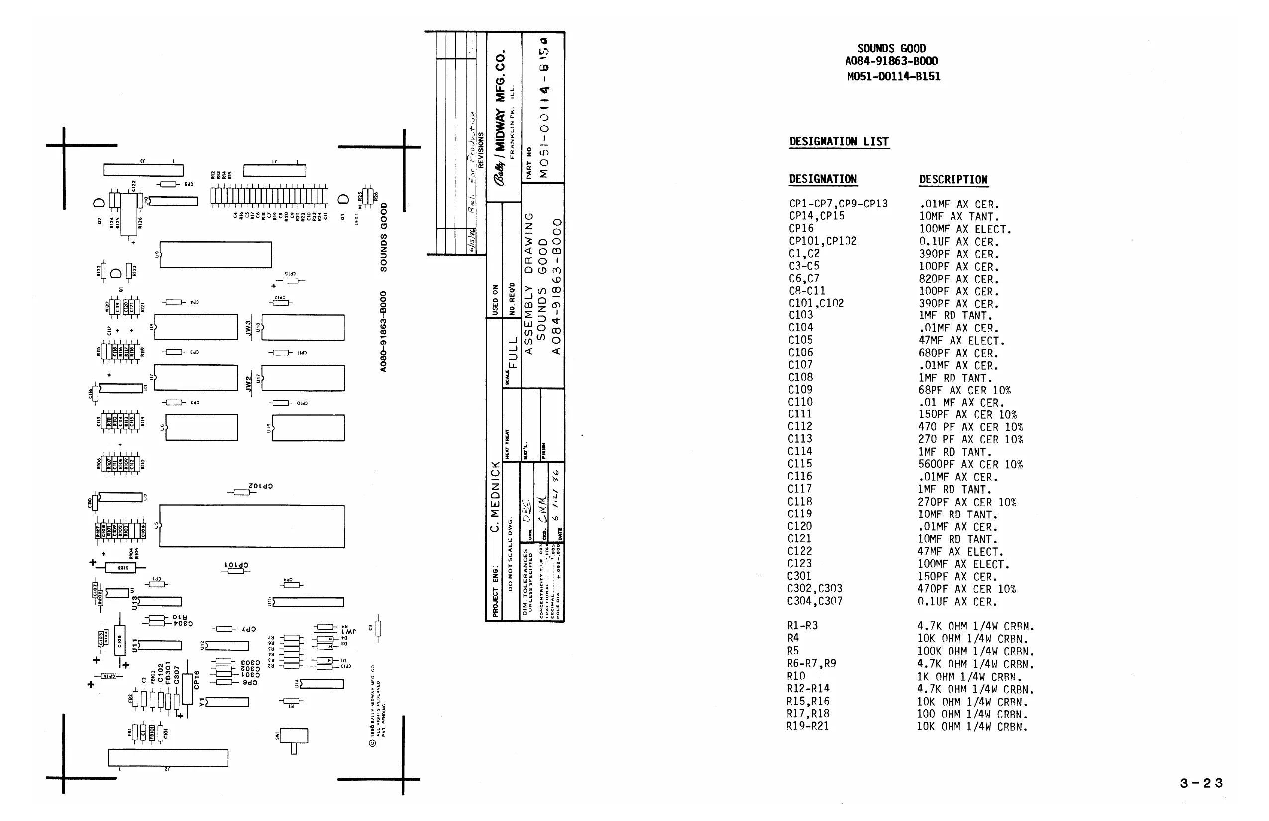
This page is a drawing, shown as the original scan.
DESIGNATION LIST
DESIGNATION
R22 R23 R24 R25 R26 R101 R102 R103 R104 R105 R106 R107 R108 R109 R110 R111,R112 R113 R114 R115 R116 R117 R118 R119 R120 R121 R122 R123,R124 R125 R126 R127 R202 D1 D3-D4
Q1-03
ul U2 ,U3 U5 U6 U7,U8 u9 u10 ULL ul2 u13 DESCRIPTION
100K OHM 1/4W CRRN. 10K OHM 1/4W CRBN. 100K OHM 1/4W CRRN. 100 OHM 1/4W CRBN. 47K OHM 1/4W CRBN. 12K OHM 1/4W CRBN. 160K OHM 1/4W CRRN. 100 OHM 1/4W CRBN. 330K OHM 1/4W CRBN. 24K OHM 1/4W CRBN. 3.3K OHM 1/4W CRBN. 24K OHM 1/4W CRBN. 150K OHM 1/4W CRBN. 82K OHM 1/4W CRBN. 510K OHM 1/4W CRBN. 120K OHM 1/4W CRBN. 33K OHM 1/4W CRBN. 330K OHM 1/4W CRBN. 150K OHM 1/4W CRRN. 33K OHM 1/4W CRBN. 18K OHM 1/4W CRBN. 100K OHM t/4W CRBN. 510K OHM 1/4W CRBN. 47K OHM 1/4W CRBN. 1K_OHM 1/4W CRBN. 2.7K OHM 1/4W CRBN. 360 OHM 1/4W CRBN. 180 OHM 1/4W CRBN. 2.7K OHM 1/4W CRBN. 560K OHM 1/4W CRBN. 100 OHM 1/4W CRBN. NOT INSERTED 1N5817
2N5305
MC 3340 LM359 6800068 CPU RAM 2K X 8 ROM/EPROM 6821 P.I.A. AD7533UN DAC 14584 /40106 74874 74LS04 SOUNDS GOOD A084-91863-8000 M051-00114-B151 DESIGNATION LIST
DESIGNATION
U14 U15 U16 U17 ,U18
FB1,FB2 FB101,FB102 FB301
ICS US ICS U6 ICS U7,U8 ICS U9 Ics U10 IcS U15 ICS U16 ICS U17,U18
Jl J2 J3
JW1-JW3
LED 1
Sw1
Y1 DESCRIPTION
74F 32 SGO1RO PAL RAM 2K X 8 ROM/EPROM
FERRITE BEAD FERRITE BEAD FERRITE BEAD
64 PIN IC SOCKET 24 PIN IC SOCKET .600 28 PIN IC SOCKET 40 PIN IC SOCKET 16 PIN IC SOCKET 24 PIN IC SOCKET .300 24 PIN IC SOCKET .600 28 PIN IC SOCKET
AUTO INSERT PIN TIN .025 SQ. AUTO INSERT PIN TIN .045 SQ). AUTO INSERT PIN TIN .025 SQ.
ZERO OHM RESISTOR
GREEN LED
SWITCH PC MTG.
16 MHZ XSTAL OSC. GROSS REFERENCE DESCRIPTION
68 PF AX CER 10% 100 PF AX CER 150 PF AX CER 10% 270 PF AX CER 10% 390 PF AX CER 470 PF AX CER 10% 680 PF AX CER 820 PF AX CER 5600 PF AX CER 10% -01 MF AX CER
0.1 UF AX CER 1 MF RD TANT 10 MF AX TANT 10 MF RD TANT 47 MF AX ELECT 100 MF AX ELECT 100 OHM 1/4W CRRN
180 OHM 1/4W CRRN 360 OHM 1/4W CRBN 1K_OHM 1/4W CRBN 2.7K OHM 1/4W CREN 3.3K OHM 1/4W CRBN 4.7K OHM 1/4W CRBN
10K OHM 1/4W CRBN
12K OHM 1/4W CRBN 18K OHM 1/4W CRBN 24K OHM 1/4W CRBN 33K OHM 1/4W CRBN 47K OHM 1/4W CRBN 82K OHM 1/4W CRBN 100K OHM 1/4W CRBN 120K OHM 1/4W CRBN 150K OHM 1/4W CRBN 160K OHM 1/4W CRRN 330K OHM 1/4W CRBN 510K OHM 1/4W CRBN 560K OHM 1/4W CRBN
1N5817
2N5305
T4LS04 T4F 32 ra NM OPNAYDYE GUNNNYNSS NER WANE
PN NME NUN PENNY NEE
won
ee DESIGNATION
c109 (3-C5,C8-C11 €111,C301 c113,C118 €1,C2,C101,C102 C112,C302,C303 C106 C6,C7 c1is C104,C107,C110 C116 ,C120,CP1-CP7, CP9-CP13 £304 ,C307 ,CP101 ,CP102 €103,C108,C114,C117 cP14,CP15 C119,C121 C105,C122 CP16,C123 R17,R18,R25,R103, R202 R125 R123,R124 R10,R121 R122 ,R126 R106 R1-R3,R6-R7 RO R12-R14 R4,R15,R16,R19-R21, R23 R101 R117 R105,R107 R113,R116 R26,R120 R109 R5,R22,R24,R118 R111,R112 R108,R115 R102 R104,R114 R110,R119 R127
03-D4
Q1-03
U13 ul4 PART NUMBER
0307-00800-N011 0304-00800-0001 0307-00800-0010 0307-00800-0009 0986-00800-3000 0307-00800-0008 0358-00800-0002 0304-00800-0002 0307-00800-0007 0986-00800-2200
0986-00800-0200 0307-00800-0004 0986-00800-0700 0307-00800-0005 0307-00800-0003 0307-00800-0006 100E-00005-0033
100E£-00005-0039 100E-00005-0048 100 -00005-0061 100E-00005-0071 100E-00005-0074 100£-00005-0079
100E -00005-0088
100E-00005-0090 100E -00005-0093 100E -00005-0097 100E -00005-0100 100E-00005-0104 100E-00005-0112 100E -00005-0115 100E-00005-0118 100E-00005-0120 100E-00005-0121 100E -00005-0128 100E-00005-0133 100E -00005-0134
103£-00003-0009
0360-00802-0012
0304-00803-0060 0304-00803-0059
SOUNDS GOOD A084-91863-B000 MO51-00114-B151 CROSS REFERENCE BALLY HIDHAY SHEET 1 OF 3 [REY EE
| DESCRIPTION | QTY. | DESIGNATION | PART NUMBER | i |
| 74874 | 1 | U12 | 0304-00803-0061 | H 7 |
| 14584/40106 | 1 | ull | 0304-00803-0056 | &é| 2 |
| 6821 PIA | 1 | ug | 0304-00803-0054 | on BF |
| 68000G8 CPU | 1 | U5 | 0304-00803-0051 | ge 2s |
| AD7533JN DAC | 1 | U10 | 0304-00803-0055 | |
| SGOLRO PAL | 1 | u15 | 0E36-00803-0009 | |
| LM359 | 2 | U2,U3 | 0304-00803-0053 | |
| MC3340 | 1 | Ul | 0358-00803-0002 | |
| RAM 2KX8 | 2 | U6,U16 | 0304-00803-0057 | |
| ROM/EPROM | 1 | U7 | ||
| ROM/EPROM | 1 | us | SEE ROM/EPROM | |
| ROM/EPROM | 1 | UL7 | CHART | |
| ROM/EPROM | 1, | u18 | ||
| FERRITE BEAD | 5 | FB1,FB2,FR101,FB102, 0316-00804-0002 |
FB301
| 16 PIN IC SOCKET | 1 | ICS U10 | 110E-00001-0003 |
| 24 PIN IC SOCKET .300 | 1 | IcS U15 | 110£-00001-0009 |
| 24 PIN IC SOCKET .600 | 2 | ICS U6,U16 | 110£-00001-0007 |
| 28 PIN IC SOCKET | 4 | ICS U7,U8,U17,U18 | 110F -00001-0010 |
| 40 PIN IC SOCKET | 1 | ICS U9 | 110E£-00001-0011 |
| 64 PIN IC SOCKET | 1 | ICS U5 | 110£-00001-0016 |
| AUTO INSERT PIN | 8 | Jl | 0304-00804-0009 |
TIN .025 SQ
| AUTO INSERT PIN | 11 | J3 | 0304-00804-0009 |
TIN .025 SQ
| AUTO INSERT PIN | 11 | J2 | 0304-00804-0010 |
TIN .045 SQ
| ZERO OHM RES | 3 | JW1-JW3 | 117E£-00001-0003 |
| GREEN LED | 1 | LED 1 | 119£-00001-0001 |
| SWITCH PC MTG | 1 | SW1 | 0986-00804-3100 |
| 16 MHZ XSTAL OSC | 1 | yl | 0304-00804-0008 |
| PC BOARD | 1 | A080-91671-G000 | canst yga |
Por 6-13-86 Released for Production, CMM. ae | 6-26-86 Rev. 1.0 CMM - Changed R101 from 24K to 12K. rik 8-05-86 Rev. 2.0 CMM - Removed D1. ae 8-28-86 Rev. 3.0 CMM - Changed C301 from 330PF to 150PF. fal? “saa aa o8@ He + 4°82 Hb» Foie ExTRESET~ Je ~ 32 PIN KKI56
ze sCF
3-26
SPARE GATES
RCBOGBOLS, ae aa
nesses 74.804 ‘ ays 6 unt vie neisie6 7aLses eae SHLD Gyo, v4
EXTRESET~ > a ae via via
] sut t\2 ‘Stes? suitor e7esersie RONTYPE REV 2 - Chonsed C301 to REV 1 REMOVED DI. 9747
NOTES ae BALLY MIDWAY RFE. CO. T FER soUNDS GoOD
18 JUNE 66 SHEET 2 OFS [Rev
a7ese-sie
vee ND vee ND ‘RON Doe
Ron] poo Der Dez a 6. De? Lue~
aporess pata ‘CONTROL ox J NOTES? aT REDNTCK BALLY MIDWAY HFG. CO.
per 16 JUNE 66 [SHEET 3_oF 5 [REV
aise est via Pim vite ee RI a RESET=34 SHEET 4 oF 3 Tnev
ensaes c at J - 12 PIM KKIE0 [Ps 4 [Ps 5 [P>s3 8
ANALOG _oUT]
BIR sev_4 RV _SENSE REV 1.8 6-26-86 R101 CHANGED TO 12K. CHM
NOTES c. MEDNTCK RALLY MIDWAY HFG. CO.
T PER 10 JUNE 66 [SHEET SOF 5 [REV
DESIGNATION LIST
DESIGNATION NO.
61,02 c3,C4 €5,C6 c7=c10
cel £P2,CP3
R1,R2
WSA1,2
MH1-MH4 DESCRIPTION
4.7 MF 25V RD TANT 22 MF 6V RD TANT 470 MF 6V AX ELEC +1 MF SOV AX CER
220 MF 25V AX ELEC «1 MF SOV AX CER
2.7K OHM 1/4W 5% CRBN 27 OHM 1/4W 5% CRBN 1 OHM 1/2W 5% CRBN
MB37 50
7 PIN 5 PIN
HEATSINK ASSY
1/4" SPACER MCR/2 DUAL POWER AMP. PC. A082-90910-F000
PROJECT ENG ?C.MEDNICK
DIM. TOLERANCES. UNLESS OTHERWISE SPEC CONCENTRICITY T1.R. . 002 FRACTIONAL . 2.164 DECIMAL HOLE DIA. ANGLE ¥ DO NOT SCALE DWG. Use0 on TRON THIS DWG IS CONFIDENTIAL & PROPERTY OF BALLY/MiDWAY MFG CO CROSS REFERENCE LIST
DESCRIPTION
«1 MF SOV AX CER 4.7 MF 25V RD TANT 22 MF 6V RD TANT 220 MF 25V AX ELEC 470 MF 5V AX ELEC
1 OHM 1/2W 5% 27 OHM 1/40 5% 2.7K OHM 1/4W 5%
™B3730
TIN .045 SQ PINS
HEATSINK ASSY
1/4" SPACER
PC BOARD
DATE 6/14/84 4 ee Qty DESIGNATION NO.
6 C7-C10, CP2, CP3 2 c1,C2 2 C3,C4 1 cP 2 5,06
4 R5-RB 2 R3,R4 2 R1,R2
2 U1, U2
12 J1,52
2 HSA1,2
4 MH1-MHA
DUAL PWR AMP ASSEMBLY DRWNG A084 -90910-FO00 PART NUMBER
0986-00809-1100 0986-008U0-3100 0986-00800-1600 0986-00800-3200 0986-00800-1700
0062-02603-1XXX 0062-0688 3-1 XXX 062-199B3-1XXX
(0066-188XX=-XX4X
0017-00033-94380
A986-0001)-E000
0017-00042-0320
A080-909 10-F 000
REVISIONS PART NO. MO5 | -00986 —FOIO
Vv AUDIO
N.C. L. AUDIO L. SHIELD KEY VAUDIO RETURN
R. AUDIO R. SHIELD V AUDIO OBNoOaaan—
R SHIELD
| vaunlio >>— | a | ? | - | —_———————B TO CHiPs |
CPI cP2 cP3 220UF 25V Le J AUF Vv AUDIO —>— PROJECT ENG: C.MEDNICK RETURN = THIS DWG. IS CONFIDENTIAL & PROPERTY OF BALLY/MIDWAY MFG. CO. DIM. TOLERANCES cigs UNLESS OTHERWISE SPEC. DATE aa ally |MIDWA Y MFG. co.
| CONCENTRICITY TLR. | 002 | 6/14/84 | | se | FRANKLIN PARK, IL 60131 |
| FRACTIONAL | +164 | 7 | r | : |
| DECIMAL | +005 | ° | . | DUAL POWER AMP |
HOLE DIA. .... +.002—.000 SCHEMATIC ile
| ANGLE ... | + 2° | [ee | © | — | — | [tee | on |
DO NOT SCALE DWG. A080— 90910— F000 MO5!1-00986-FOII REVISIONS
BRUNING: 40-107
3-30
NOTES! UNLESS OTMERwise SPECUREDL Web a) cet ary
- CaPaciroR VAWES 'N MicRarARADS /VOLTS. \. TEsisroR Vaues APE IM OHMS Yaw, 5%, CF. FOR ADDITIONAL ELECTRICAL INFORMATION, REFER TO MECH. DWG. NO. 0017-00003-0543. ee a ee Opi @ ia
+ cue, 1000/y5, -
@ji2vAa em
@pi2v @ 4a ©)
cst 1000 /yg =“ + ore
- Oe/ag A @ 0) @) +5v Qi2za 9) + @ +|Ca7 Co
722 @ o ©
- @ (| com ® () + © cs? Bo, @ f ™
©} -Sv @1a
9 - @| cer OPTOCOUPLER Rie COB 10/50 a
zs von,
v2
TLanceP ear Om 1%
M05 1-00945-A087 = —
CAMARILLO, CALIF 93010 (003) 400-2031
SP\OI® inet ‘ sade ia (00 NOT SCALE ORRAWING,
This page reads as a drawing: its text was drawn rather than typeset, and comes out in fragments. See the original scan.
FCC FILTER 8D FOR MONO BD [——J Ie. STRAP io a4 © mIge?
Keyl oh= (rms) = tee
- BALLY MIDWAY - A080-91870-A000 Li {iwi} Cr ea ib a
Coleused Foe Mofucti ors REVISIONS PROJECT ENG: C.MEDNICK usep on RAMPAGE @aly | MIDWAY MFG.CO a ee FRANKLIN PK. ILL.
ASSEMBLY DRAWING FCC. FILTER FOR MONO BD. | MOSI-OOE36-AIG6GO ( A084-91870-A000) DONOT SCALE DWG
om EC 8/2 /o6 DIM. TOLERANCES UNLESS SPECIFIED
COMCENTHICHTY Fe 00g PRACTIONAL “16a DECIMAL 7 HOLE DIA 38421386 +002 0001 pare
3-32 FCC FILTER BOARD FOR MONOBOARD PART NO. A084-91870-A000 051-00E36-A161
DESIGNATION LIST
DESIGNATION NUMBER DESCRIPTION
C1 - C3 -01 UF AX. CER. FB1 - FR4 FERRITE READ Jl CONNECTOR 12 PIN KK156 R/A J2 HEADER 12 PIN KK156 R/A OMIT PIN 5 JW1 - JW2 JUMPER WIRE KEY 1 -KK156 KEY FOR PIN 5 OF Jl
CROSS REFERENCE LIST
| DESCRIPTION | ory. | DESIGNATION NO. | PART NOS. |
| -01 UF AX. CER | 3 | Cl - C3 | 0360-00800-0005 |
| FERRITE READ | 4 | FR1l - FB4 | 0316-00804-0002 |
| HEADER 12 PIN KK156 R/A | 1 | J2 | OF 36-00804-0002 |
OMIT PIN 5
| CONNECTOR 12 PIN KK156 R/A 1 | Jl | 0E36-00804-0001 | |
| JUMPER WIRE | 2 | UWL - JW2 | 117E-00001-0003 |
| KK156 KEY | 1 | KEY 1 | 0017-00021-1353 |
| P.C. BOARD | 1 | A080-91870-A000 |
8/13/86 - Released for Production - CMM 8/14/86 - Rev. 1 - corrected J1, J2 designation reversed.
Toe
Je - 12
CABLE SIDE
©
MTGH2 ae FBS = FBL
MTGH1 Ji- 12
MONOBOARD SIDE
Sie Bytes:
BALLY MIDWAY MFG. CO.
FCC FILTER BOARD M@51-@E36-A162 AG84-9187D-ABeo
SHEET 1 oF 1 TREY A
TO MONITOR
CONTROL
POWER CHASSIS: A945-20059-0200 TO SOUND BOARD 2) CONDOR POWER SUPPLY 5a) TO COIN DOOR CONN. -svf ipl ' ia eta TO MUX BOARD H METER +ieV! SBLU-ORN trav} pein. u. Roun) @BRN | 3tac NEUT GROUND! eern pti. EROUND} SyE GROUND GROUND} 19) GROUND! Pee GROUND? 12) GROUND ' 13) GROUND i 14 +54 | 15 +5¥116) +5¥ H 17) +5 i 18) +5¥ i 19 +5v {20 RIGHT L2,
DATA
[| pata 3 grounn TOWTEST BRACKET || Data 1
TO COIN DOOR CONN.
GRN-RED
GRN-BLU
GRN-BLK GRN-BRN GRN-ORN
YEL-RED
RED-BLU
RED-YEL RED-GRN. RED-ORN BLK-YEL, GROUND; GROUND] GROUND] GROUN =|2 (SIC eae orées oPp6?
TO_ MONITOR METER-RET Revli GROUND H 2 GREEN | 3 GROUND Hi 4 BLUEIS GROUND !6 i kEYI7 HBLNK~! 8 {GROUND 1+5v ie1ey IKEY FRESET_OUT IRESET_OUT {+lev {+5¥ Stercien TO COIN DOOR CONN. HOHO BoARD id age4-91787-ce0a t TPP pRu-BLk COIN 273
| VeRounn | | OU gencveL | START 1 | |
| iGROUND | | | SIF aRn-RED START 273 | |
| 1e5¥ | H | RED-WHT | STATUS |
{+5¥
| key | H | ORN-HHT | ___SERVICEy © TO TEST BRACKET |
| }RESET_OUT | H | GRY-RED | TEST, |
{GROUND ietav UP RI 1+5¥ telesy
| JO LAMP BOARD | 11 1GROUND | terete |
t 1 IP13113
| TO AUDIO AMP BOARD | 12)6ROUND | KEVI14 |
TO SOUND BOARD IPi4tis
- IP15116 IP16117 IPi7118 GROUND {19 ‘@BRN-HH
TO SOUND BOARD
GROUND LINE VOLTASE SELECTION CHART VOLTAGE | 185 115 ) 210 ) 220 | 230 | 240 COLOR JUMPER 1] 5-1 11] 8-14] 11-14] 11-14] 11-14| a0RN JUMPER 2]14-15]14-15] ouT | OUT | OUT BALLAST Jumper 3! 4-7 ' 4-10! 4-7 ' 4-7 V 4-10! 4-13! oreD TO CONTROL CONN. A BS4,
TO MONO BOARD J5 HHT-RED, ]HT—BLU.
MONITOR
uP_R3 DOWN RS LEFT R39 HHT-YEL, RIGHT RG_WHT-GRN DOWN LS WHT-BRN LEFT _L3__HHT-ORN RIGHT L3 WHT-ERYJ PLR 273 _BRN-GRI
}41GROUND [> To CONTROL CONN. SivsYNc wm HOHER ‘Chassis [> To LIGHT CONTROL PC SyHeync [NoTEs? BALLY MIDWAY HFG. CO. 7} @RouND R.A. PLOUSSARD 2 iysyNc~ JAN 16 1987 STAR GUARDS 3] HSYNC~ CABINET WIRING = 18AHN6 3ea8y N@51-80E89-AGO3 = LGHS. 690¥ SHEET 1 OF 2 [REV
3-34
LAMP BOARD TO_POWER SUPPLY A@e4-91877-AEGS 1 1+sv TO MONO BOARD
| eRound | vel | 2 isrounn | TO_LANP_ BOARD | CONTROL C Gov py | LIGHT 1 | START 1 te *peN-vEL | peat |
9 1GROUND —
| TO CONTROL CONN. C | H | to | . | up Rt | |
| d Key | cry-reD | UP RI | de pBiu=Ren | Gl | | |
| CONTROL 9 | H | tt | DOHW Ri |
DOWN Ri =
| GRY-RED : woes | sry | ee | ee | ot | |
| CONTROL _@ | ORN-BLU, | H | TQ_COIN DOOR CONN. | it | LEFT Rt |
NHBLK. 7
| tecitar | GRY=ERN AIS {CONTROLE | 44h | LEFT RI | da j_Buu=san |
| To MONO BOARD J4 | CONTROL 1 | ORN=GEN AMV 9 | conrRoLi | Reread _js i arate | RIGHT RL |
1 1 up Li
| uP ut | BLU-BLK | ‘a | |||||
| TO_CONTROL CONNECTOR | ; ol | © | 7 | ||||
| 8 TO 4 MUXER | bom us | 1 toy gen | DoW Lt | ||||
| nge4—91881-n0N8 | a7 + | ° | + | ||||
| TOCONTROL Cy | COIN DOOR | TO COIN DOOR | START 2 | ORN=RED gS yy | LEFT Lt | de H BLU-ORN. | erat |
| LIGHTS | COIN 2 | PINK | han | ||||
| tinea | it | RIGHT Lt | |||||
| "he linea | RIGHT U1 | _j, 4 BLu-6RY | Ce | ||||
| JO POWER SUPPLY | H | ha | TO TEST BRACKET | ||||
| piev | ORN“BLK | a | START 3 | ORN-YEL i He | GROUND | 1) oe | |
| GROUND | GRY-BLK | Bie | GROUND | tt | up re | ||
| COIN METER | lB 1 INSB | To CONTROL BPP RE | i | oN | 4 | ||
| CH | nom Bonen Je | METER | MHT-YEL | Sane | mf | Dow Re | |
| I | TO_POWER SUPPLY | GROUND | To leROuND | DOWN Re | fof SRNBL | 5 | | |
| MAT | PLR 273. | BRN-GRN ABTS iKEY | LEFT RE | | -e _SRN-VEL | LEFy Re | ||
| 121A7B | isk | ° | |||||
| START 2/3 | BRN-RED Gh 3iours | tot | RIGHT | ||||
| TO_HONO BoA | en | COYN 1 | TO_HONO BOARD | [COIN 2/3 BRN-BLK GUTS | RIGHT Re | 4.44, GRN-WHT | r |
- H
| ifistours | it | up Le | |||
| COIN 2 | wer | up Le | GRN-BLK | R | |
| PINK | ieee | | | {B16jours | 415 | ° |
COIN 3
| T0_8 TO 4 MUXER | ERN | AN | 70 HoWo soaRD | control » | noun ue |
| ery | THT | DOWN L2 | Pag ce | aN | |
| YEL | to | RIGHT Le | |||
| RIGHT 12 | __j, , sRu-snv | aN |
© + H LEFT Le
| TO POWER SUPPLY | LEFT Le. | 2p SRNCORN | —o | + |
it Up RS
| UP_R2 | ds p_MiToneD | iq | |||||||
| 5 & | 2 | + | |||||||
| DOWN R3 | dg | WHT-BLU | SOAS | ||||||
| DUAL POHER AMP | a F | arava | |||||||
| Jt nee4-99910-Feae | RIGHT R3 | UHT-GRN | |||||||
| FLeVORTN | GRY aT “Te ROUND | VOL PoT HIPER[i | fpilac | we | unt | SPEAKER, | } | en | fc |
| 2 1 GROUND | AUDIO OUTI2 | eit aupro | refi | or | LEFT R3 | poravet | oN | Fs | |
| 3 1+5¥ | AUDIO OUTIS | Bit SHIELD | R12 | ? | Se | p | |||
| 4 l45¥ | ® GROUND!4 | atkey | key Iai | uP La | 4, WAT-BLK | eal | | | ||
| 5 i+tev | A GROUNDIS [ft | Biv AUDIO RETURN L+i4l® | ' | a | z | ||||
| 6 tsiev | AuDIO oUT!s fil | 61R auDIO | ucts | L_SREP | DOWK Lo | j, HHT-BRN | aN | ||
| 7 1£ GROUND | aupro ouT!7 ft | L- [ell | 4 | r | Rent Ls | ||||
| e | A GROUNDIG I | v AUDIO | RIGHT L3 | H | WHT-GRY | aN | ; | ||
| M | kevio Wt | SPEAKER | qizk | © | : | ||||
| 1 | Bg ey wy gy VOL POT Ai Lop p SK MAT | LEFT La | dik HHT-ORN | teryts | 4 | ||||
| 1 | eee SEER SS a cRounlis | TO_8 TO 4 MUXER | |||||||
| fiesee sis | ORN-BLK | TO TEST BRACKET | TEST agacxer | on | tok oT | stag | |||
| SO NOND pOeRD Je | crv-ren | TERT | START 3 | ds | ORN=VEL, | SIARY ° | z | |||
| | | io | H | To_CONTROL A | 14 | © | + £ | |||
| J] | <<} CONTROL CONN. Af YEL | 1 | H | a | GROUND | 4 i Yeu. | 5 | ||
| a | { | i | GROUND | a |
FS orn-war {SERVICE |
| Cop te towe soary ye FP yeL-ReD 1? | ' | fioweorn Bode! | aa | ||
| 2 | BLK-WHT | | H | NOTES: | BALLY MIDHAY MFG. CO. | |
| & | ! | w | | R. A. PLOUSSARD | ||
| e | TO NONO BOARD | YEL-BRN | | z| | JAN 16 1987 | STAR GUARDS |
123 | CABINET HIRING H a
| ‘1a sounin diakD | ORN-BLK | | * = 18 AWG 3e0V | 0S1-29E89-Aee3 | i |
| u | 4 | SHEET @ OF @ [REV |
8 TO 4 MULTIPLEXER
AG84-91881-AGIR M@51-88114-A181
3-36 | CROSS REFERENCE LIST
DESIGNATION
19@pF AX CER 9
-@luF AX CER 1
1@uF AX TANT 1
19K OHM 1/4W 5% RES 4 R1-R9
198K OHM 1/4W 5X RES
74HC241 | AUTO INSERT PIN .825 it
PC BOARD
DESIGNATION LIST
BOARD PART NUMBER B368-BB8HS-OBAG BIBE~BUEIS-20BH BIBE-BOEBHH-B7BH 18HE-B9285-BH888 188E-BBBWBS5-H115 BE89-B9883-B801 9384-BO8H4-DHB9 AGBH-91881-ABBR
1@uF AX TANT ~H1luF AX CER 188pF AX CER 19K OHM RES 188K OHM RES T4HC241 AUTO INSERT PINS .925 AG8BH-91881-AsIT RELEASED 18 DEC 1986 RAP R. PLOUSSARD
|PROJECT ENG: DO NOT SCALE DWG. DIM, TOLERANCES | UNtess srecirigo Loncentaicity r4.9 003 FRACTIONAL 11/64) ECIMAL. - 008 OLE DIA. +.002~.000 pare (& (2UI8E ““FULL ASSEMBLY DRAWING 8 TO 4 MUX. ( A084-91881-A0OO ) Cc © BALLY/MIDWAY 1986 ~<a} <a} e+ <a Ul
~<a} (ae -~ie + a7} r- +, J 8104 MX ™ ~ A080-91881-A000 cre
aa aay Za co 33> Co > Ce t+ 6G TZ a 4 cs
i REVISIONS @alty, | MIDWAY MFG.CO. FRANKLIN PK. ILL.
usep on OE 89 No.REQ’D | PER PART NO. BD. MO51-O0114 -A180
z74nce41 ial 1¥1 1A2 GROUND PIN 10 | POWER PIN 20 NOTES? BALLY MIDWAY MFG. CO.
R.A. PLOUSSARD DEC 19 1986 8 TO 4 MULTIPLEXER AG84-91881-ABBe M@51-00114-A182 SHEET 1 OF 1
BALLY/MIDWAY'S STAR GUARDS (3 PLYR) UR. F0E89 ROM/EPROM PART NUMBERS
UNPROGRAMMED MONOBOARD A084-91787-F000 PROGRAMMED MONOBOARD A084-91787-AE68
JUMPERS IN OUT JWl ¥*F JW2 JW3 Pos. MIDWAY PART NUMBER I5A __0E89-00803-0006 14B OE89-00803-0007 8E 0E89-00803-0013 6E OE89-00803-0012 5E 0E89-00803-0011 qE OE89-00803-0010 3B 0E89-00803-0008 5B 0E89-00803-0009 5H £ 0986-00803-9200 | ae UNPROGRAMMED SOUNDS GOOD BOARD A084-91863-B000 PROGRAMMED SOUNDS GOOD BOARD A084-91863-AE68
| Pos. | MIDWAY PART NUMBER | JUMPERS | IN | OUT |
| UIT | 0E89-00803-0002 | JW1 | + | |
| U7 | 0003 | JW2 | Lcd |
RK TW3 = OE89-00803- UIs OE89-00803-0004 U 0£89-00803-0005
M051-00£89-A008 REVISIONS
01-20-87 RELEASE FOR PRODUCTION