Red Baron Sit-Down DP-171-1st-02A
Red Baron (revised hardware) (Atari, 1980) · Drawing Package · 1 pages · original scan
Clock Ci
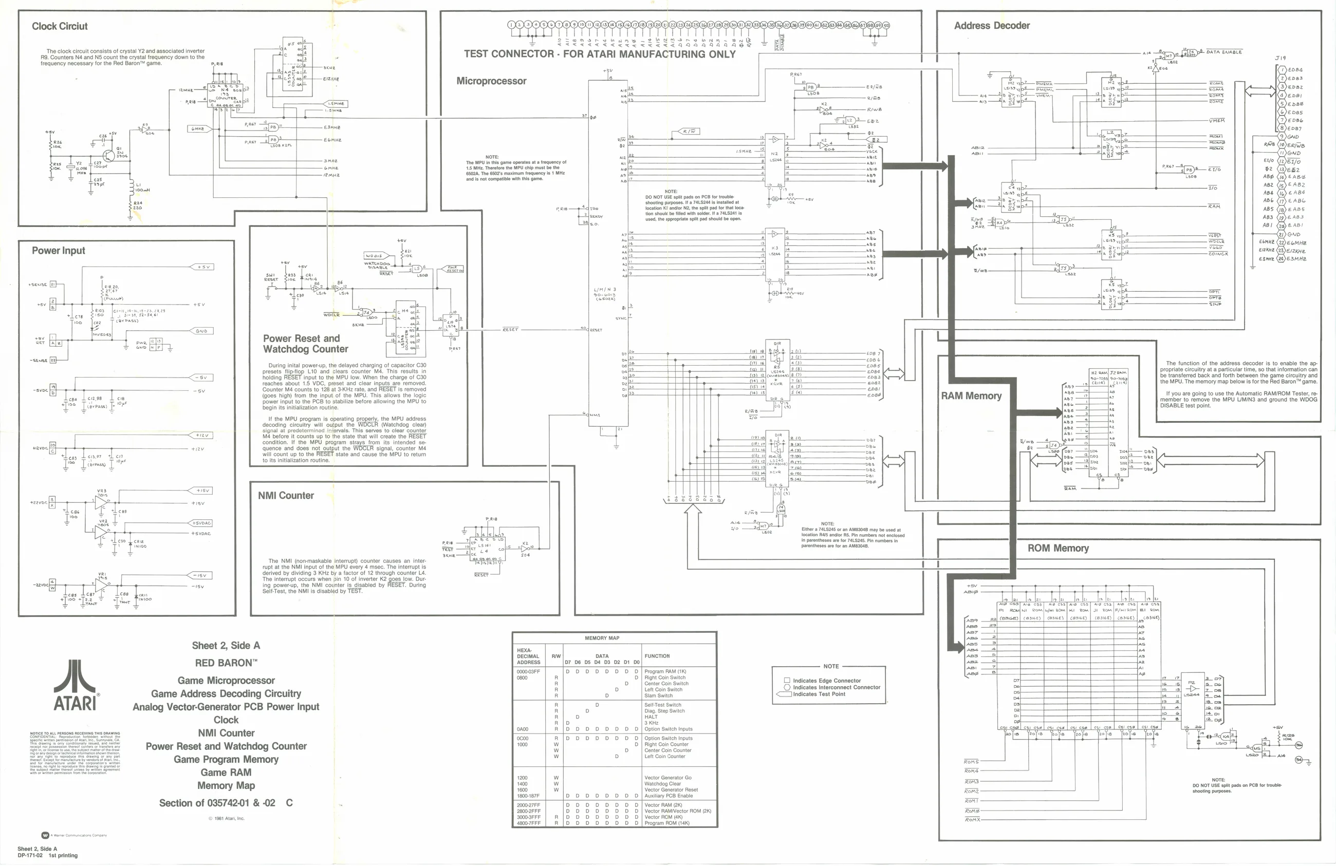
‘The clock circuit consists of crystal Y2 and associated inverter
R9. Counters N4 and NS count the crystal frequency down to the
frequency necessary for the Red Baron™ game.
ernie
cme]
Microprocessor
Esme
eomne
oa F fone
- ievoney
Sheet 2, Side A
Nore The MPU In this game operates at trequency of {LSM Tharalre the MPU chip must be the 502A. The 68s masimum lrequoncy let MME nd not compatne with this game. nore 100 NOT USE spit pags on PCB for trouble r.S244 I tale at {ocationK nalor N2 tho spit pa fr tat loca tion sho be filed wih soe a 744.5241 fo sed the spropiat split ped shouldbe open ‘shooting purposes.
meee - Power Reset and al
Watchdog Counter
During inital power-up, the delayed charging of capacitor 030 presets ‘L10 and clears ‘counter Ma. This results in holding ‘input to the MPU low. When the charge of C30 ‘reaches about 1.5 VOC, preset and clear inputs are removed. Counter M4 counts to 128 at 3KHz rate, and RESET is removed (Goes high) from the input of the MPU. This allows the logic ower input fo the PCB to stabilize before allowing the MPU to begin its initialization routine.
the MPU program is operating property. the MPU adass decoding circuitry will oufput the (Watchdog clear) ‘Signal at predotermined ‘ssorvala, This serves to clear counter M4 before it counts up to the state that will create the RESET Condition. If the MPU program strays from its intended se- ‘quence and does not outgut the signal, counter M4 stil count up to the RESEF stato and cause the MAU to retum 10 its initialization routine.
NMI Counter
The NMI (non-maskable interrupt) counter causes an inter rupt at the NMI input of the MPU every 4 msec. The interrupt is derived by dividing 3 KHz by a factor of 12 through counter Lé. ‘The interrupt occurs when pin 10 of inverter K2 goes low. Dur Ing power-up, the NMI counter is disabled by uring Self-Test, the NMI is disabled by TEST.
RED BARON™
Game Microprocessor Game Address Decoding Circuitry » ATARI Analog Vector-Generator PCB Power Input Clock
sence roa reson neceme re naw NMI Counter
Power Reset and Watchdog Counter
‘ai Game RAM Memory Map
Section of 035742-01 & © 1861 Aa
DP-171.02 ‘st printing Game Program Memory
02 C The function of the address decoder Is to enable the appropriate circuitry ata particular time, so th be transferred back and forth between the game circuitry and the MPU. The memory map below is for the Red Baron™ game. If you are going to use the Automatic RAMIROM Tester, re- ‘member to remove the MPU UIMIN3 and ground the WOOG DISABLE test point.
Esther a 7415245 o an AMSSOAB rey bo use at locaton AS ance. In parethesos are for 745245. Pin nubs in parentheses ae for an AMB2O48. numbers nat enclosed
ROM Memory
t Tk The
Fr nee
FUNCTION
Program RAM (TK) Right Coin Switen Center Con Switen Left Coin Switen Slam Switzh Interconnect Connector <—indicates Test Point
SeitTest Switch Diag. Step Sitch HALT SKHe Option Switeh Inputs €SS2\222220|n0202 ‘Option Switch Inputs Right Coin Countor Canter Coin Counter Left Coin Counter
Vector Generator Go Watchdog Clear Vector Generator Reset Auxlary PCB Enable E
Vector RAM (2K) \Veotor RAWIVector ROM (2K) ‘Vector ROM (tk) Program ROM (144)