Cloak & Dagger SP-242 1st Printing
Cloak & Dagger (rev 5) (Atari, 1983) · Schematic Package · 20 pages · 36 sections · original scan
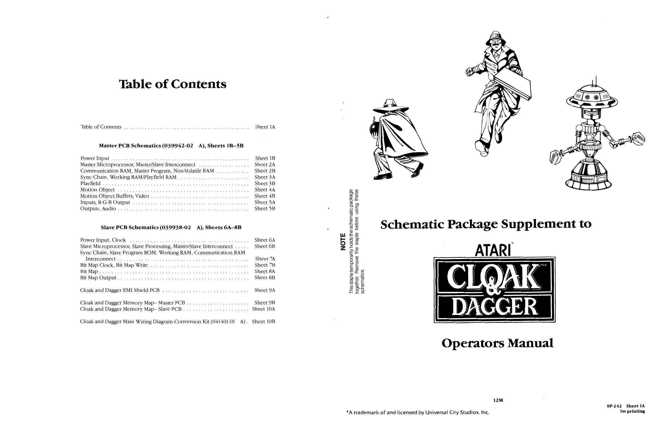
Table of Contents
Table of Contents beans Peet ene te nem ee e . Sheet 1A
Master PCB Schematics (039942-02 A), Sheets 1B-5B
Power Input eee te its vee hemmge: geese i et Sheet 1B Master Microprocessor, Master/Slave Interconnect a Sheet 2A Communication RAM, Master Program, Non-Volatile RAM ........ - Sheet 2B Sync Chain, Working RAM/Playfield RAM... 0.000 00000000 c 000 Sheet 3A Playfield... tesipt eee cette eee esse ee eee. Sheet 3B Motion Object Pe yew 28d tiggne eee eee veceeeese.. Sheet 4a 2% Motion Object Buffers, Video . . . rrr rere cess... Sheet 4B gs Inputs, R-G-B Output»... 0.0.0.0. bec eeee Sheet SA Zo Outputs, Audio... ... . tame sees beeeee .. Sheet 5B 25 el Eo 25 4 Slave PCB Schematics (039938-02 A), Sheets 6A-8B 3B Schematic Package Supplement to £o Power Input, Clock ......... rn vevceeseeees Sheet 6A 53 cy Slave Microprocessor, Slave Processing, Master/Slave Interconnect .. Sheet 6B 23 Sync Chain, Slave Program ROM, Working RAM, Communication RAM Ze Interconnect . . . ea ae pines se ewes oe ee Sheet 7A 56g Bit Map Clock, Bit Map Write ........... . a ... Sheet 7B fe Bit Map . a . cence eee .. Sheet 8A 228 Bit Map Output............... ee bees bee Sheet 8B o5a Cloak and Dagger EMI Shield PCB . . tag . vo. Sheet 9A £893 Cloak and Dagger Memory Map- Master PCB . . a ; ... Sheet 9B Cloak and Dagger Memory Map- Slave PCB bees : .. Sheet 10A
Cloak and Dagger Main Wiring Diagram-Conversion Kit (041401-01 A). Sheet 10B
Operators Manual
12M SP-242 Sheet 1A *A trademark of and licensed by Universal City Studios, Inc. Ist priating
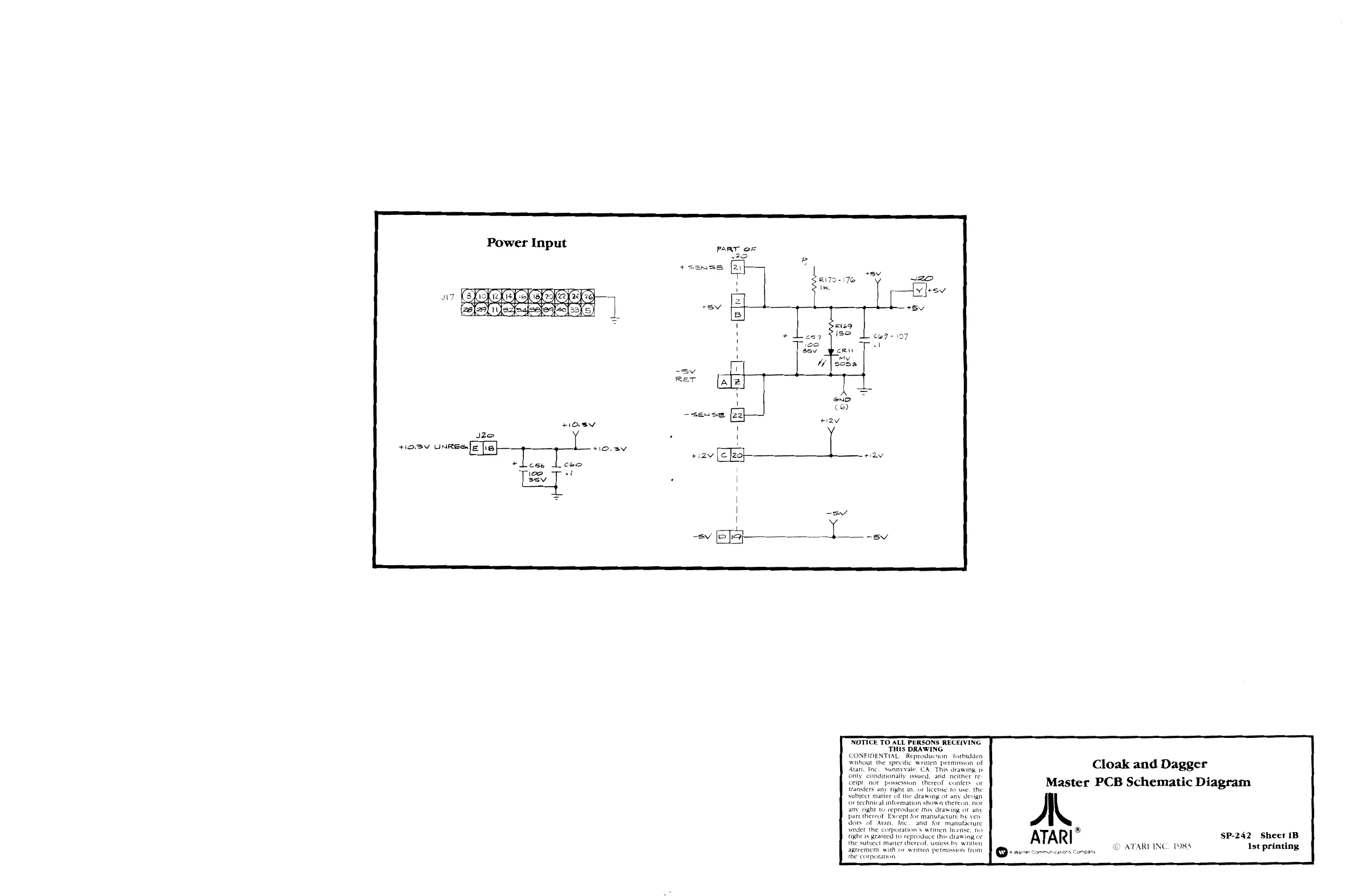
This page is a drawing, shown as the original scan.
jececan
+OSBV UNKES +5V
Re 1oK a3]
An|
an
aie]
rc cop spRoeS
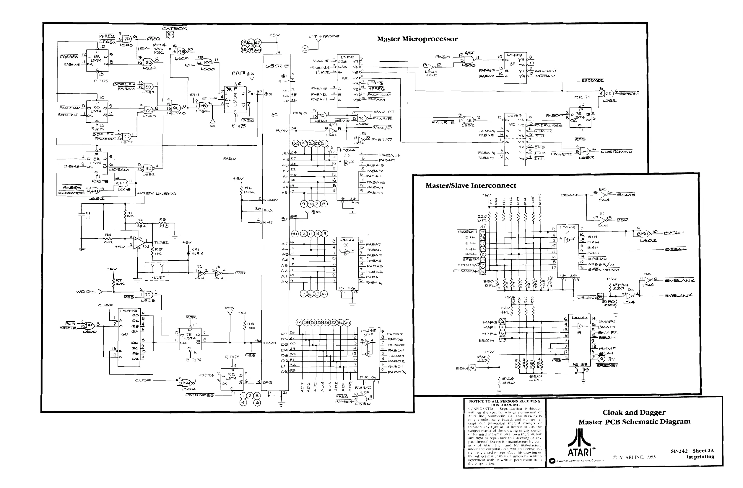
Master Microprocessor
Fi
ps 2 Ex 2 po ss 19 x 2 ) Master/Slave Interconnect
tov
>. Ie
aan & ; se aoe sae carr
ein
e2H
eau eeu EPBRSLS) eraerKy, aoa)
Ls245
Slap a S-mAaDe 13 —paacs 4 S 2 paso4 | Preieaaeaed HI BOOZ 7 3 2 exec: 3 <paacy
NOTICE TO ALL PERSONS RECEIVING THIS DRAWING CONFIDENTIAL Reproduction forbidden without the specitic written permission of Atri, Ihe. Sunnyvale, CA This drawing 1s only conditionally issued. and) neither ce ceipt nor possession thereof Confers or Transfers any right in, or license to use. the subject matter Of the drawing or any design ‘Or technical information shown therenp, nor
any right to reproduce this drawing of any
pars thereat Except for manufacture by ven: sors of Atan. Ine, and for manutucture Under the coxporagon's written license. no ght ss geanted to repextuce this drawing OF the subject matter thereor unless by written agreement with ve written permission from, the corporation Cloak and Dagger
Master PCB Schematic Diagram
A.
ATARI
SP-242 Sheet 2A ATARI INC. 1984 Ist printing
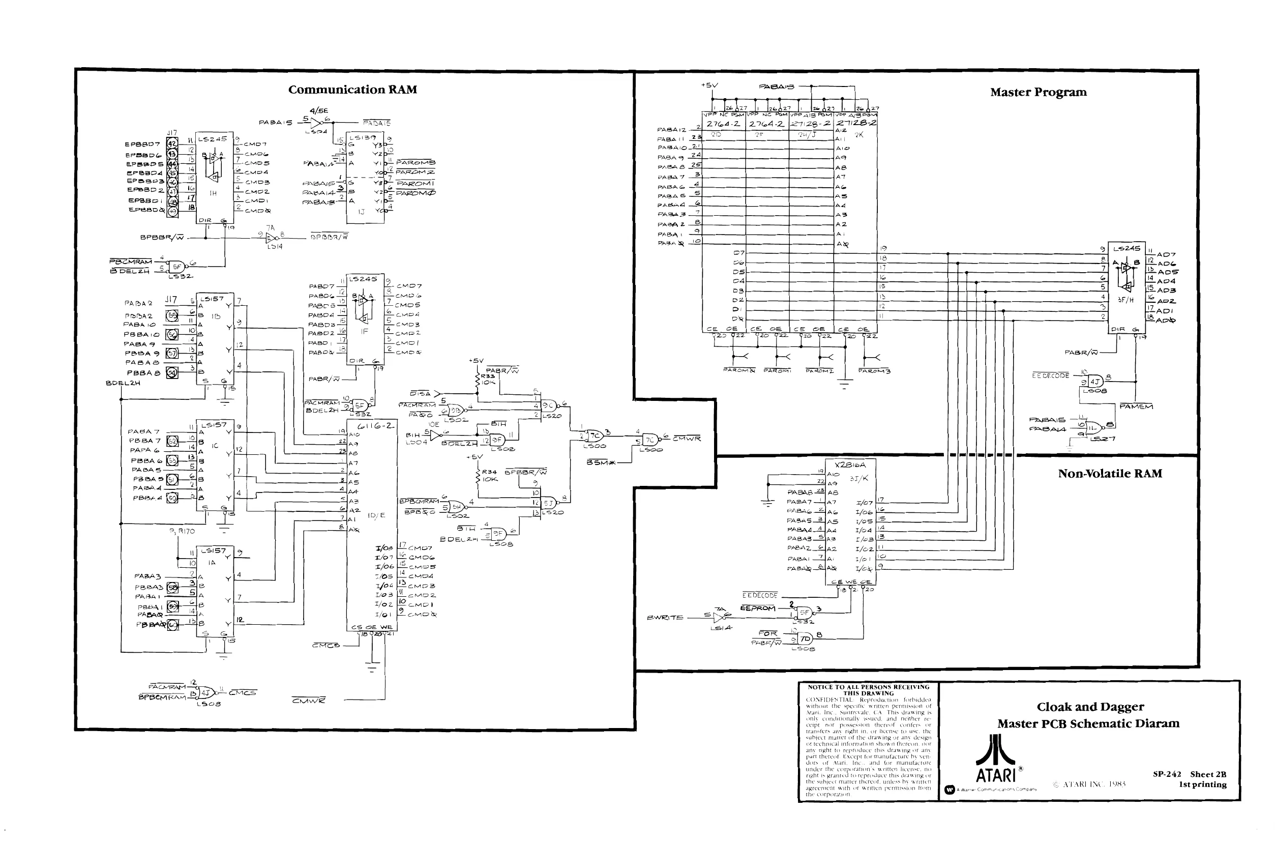
This page is a drawing, shown as the original scan.
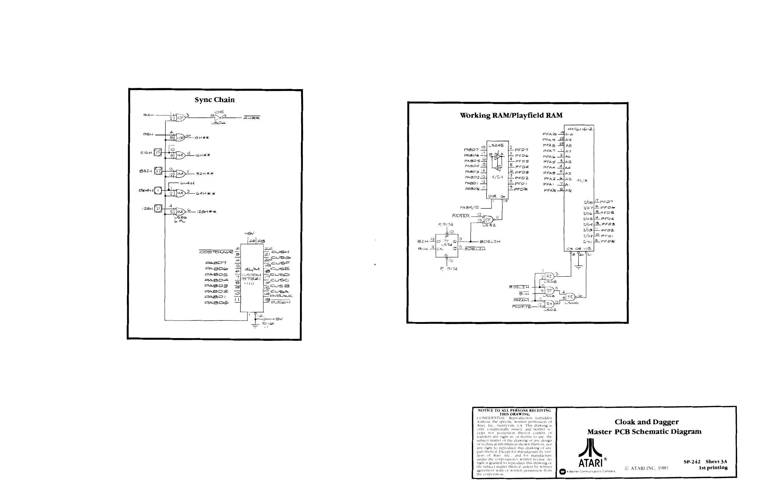
This page is a drawing, shown as the original scan.
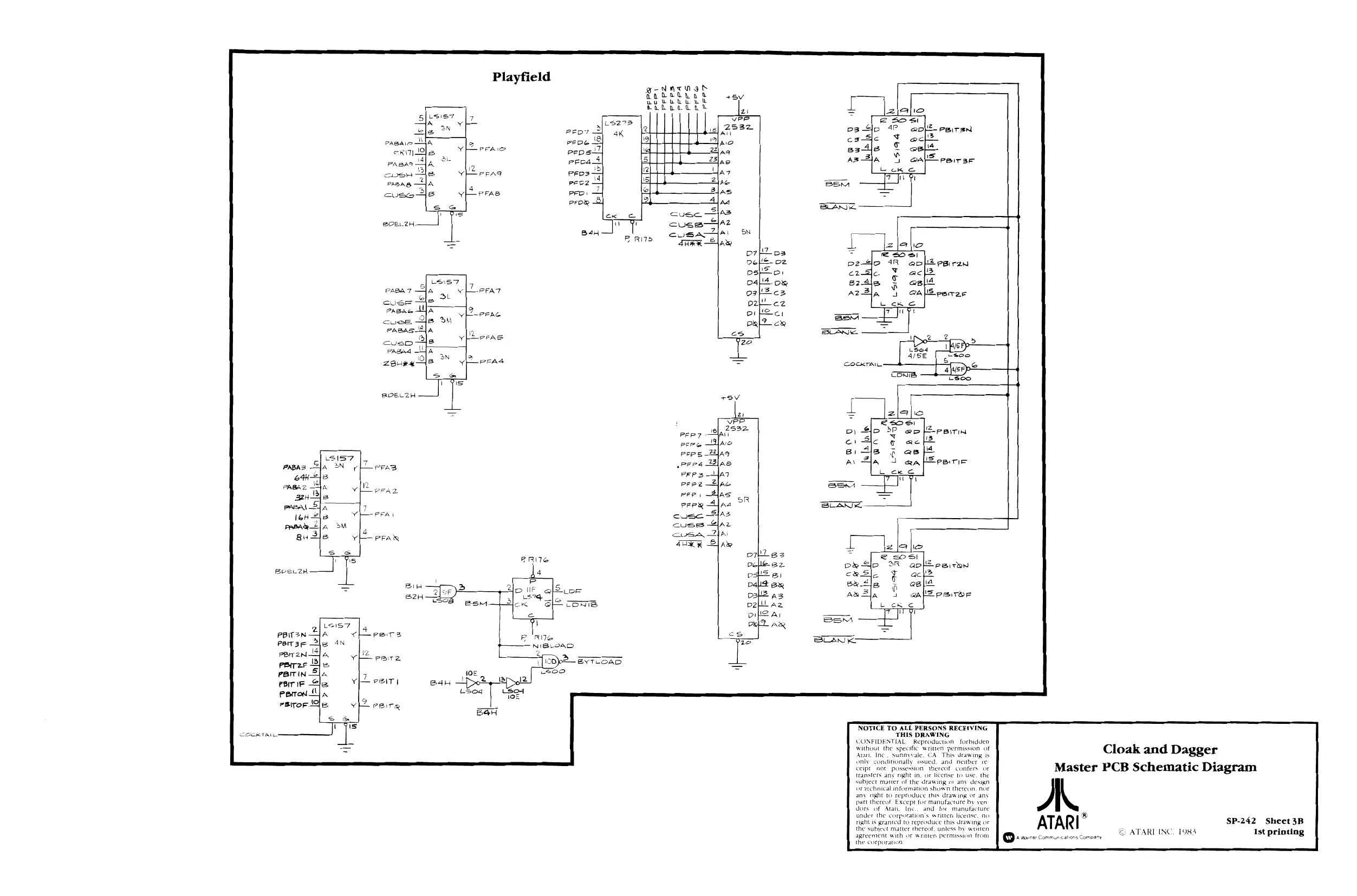
Playfield
i rasaio exit}
Pagar
ever PABA aus6
Le aire [5 fia HSeerac
4/5 coeur Tafa) e uséo
RDELZH
N [2 i q eh IN Lata lw PROD RHHL IE
Ir id In Ei
of 12 pai TON
ia BveL24 od
Dat Bx ost2 as eA}S peiTOr Lh aa. be De
- te —fey_erceas Tr
2 very
}2 cary
NOTICE TO ALL PERSONS RECEIVING
CONFIDENTIAL Reproduction forbidden without the specific writen permission of an hus inc sal CA The Sawing Cloak and Dagger cei ne ponawsn ere conters Master PCB Schematic Diagram transtere any ight in. oF hicnse fh Use. the subject matter ofthe drawing e# anv. design Griechinal information shown thereon. Not any sight to reproduce this drawing st any mart thereat Eaceptior manufacture by ven Gots Of Atan Ine. and. for manufacture Sader the corporation's maitien license. no fia is granted to reproduce ts Grawing ATARI SP-242 Sheet 3B the subject matter thereat. sinless be ween © ATARIING., (Gad ist printing agreement with or waiten permission ton) [a qure conmncators comsany the comporaten
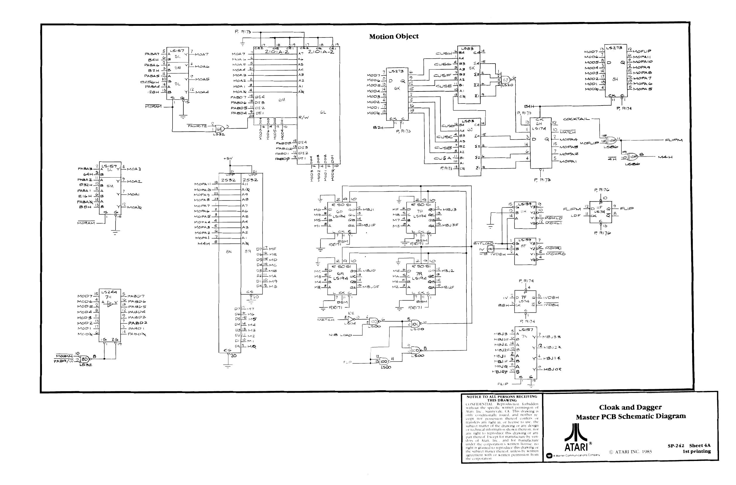
This page is a drawing, shown as the original scan.
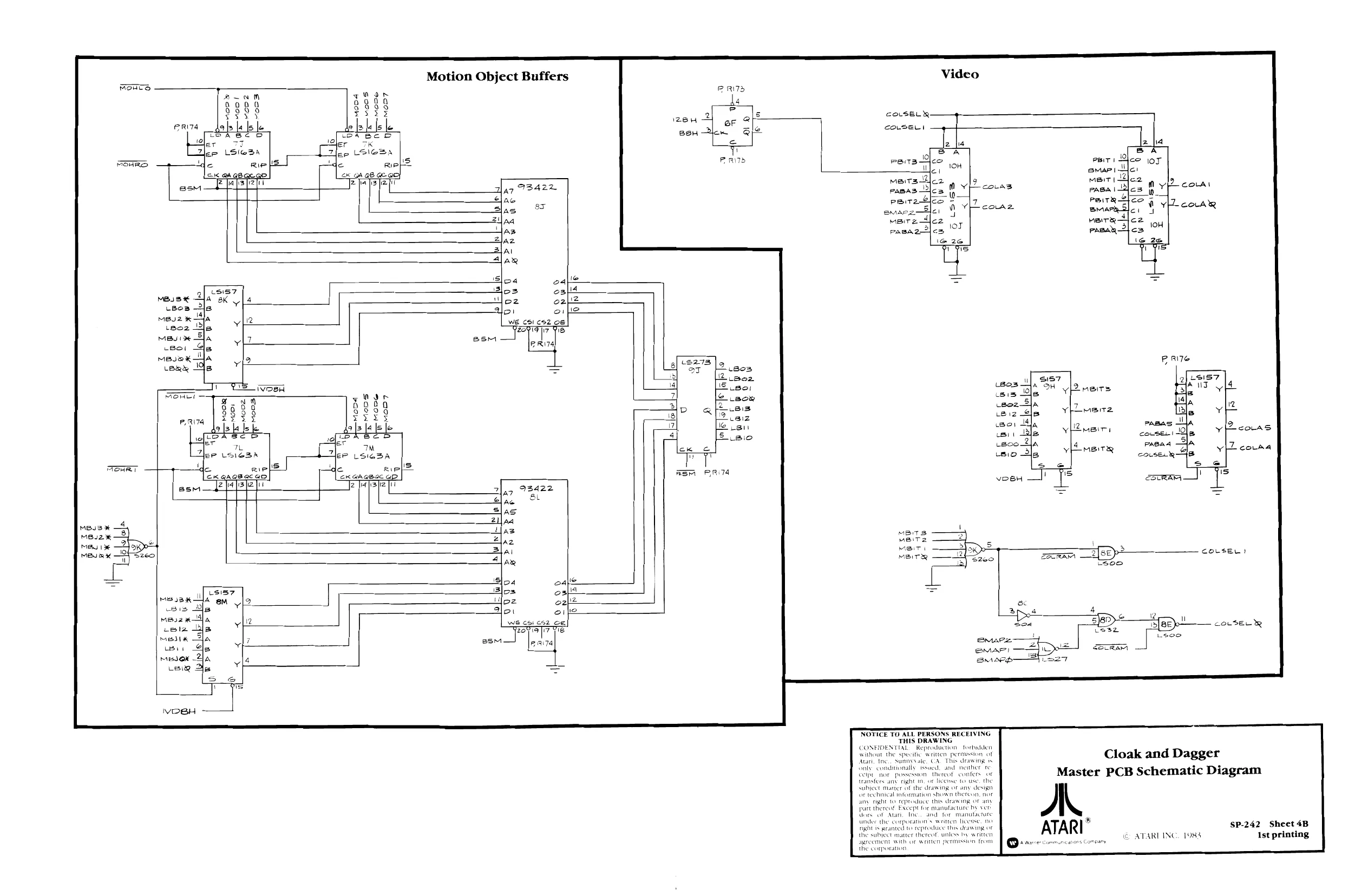
MBI3 *
MU MBv2*
MeN RK S260
Motion Object Buffers
iz fir aa7 73422
Se 8x Slas 24 04 Az Zlaz Al AR
oa o4 Bos oati4 oz o2p2 Boi oie
JEP LSIGBA le kip] EK GAGBSC GD is
fe fapispe yl rt WE C61 652 08
2|,5 93422 a7 ae ela. ot slas 2 aa AZ
Az, fi z
Zhai
AR
slog alle. los osl4 Woz ozlZ Aoi ope
We coics2 Ce POST Vis
eRIT4 My mem PRI ol’, 12 errs LsozS{a 7 tez4e 9 Yp>uere i4 wei ala vases te Pd a cee. I yi2couas 2 5 iscota 4 papas 7 [4 reir, |Z corma Lsio le, Y R couse a4 Y
NOTICE TO ALL PERSONS RECEIVING THIS DRAWING CONFIDENTIAL. Reproduction Torhatden without the specific written permasion of Atari, Ing,, Sumnysale, CA. This drawing is bile condiionally sued aaah neither te ceipt hor possession thereot confers ar transfers and right iff Ticetise to Use Subject matter oF the drawing or any design, Gr technical information shown thereon, nor any eight to reproduce this drawing er any part thereat Except for manutacture by ver Unies oF Atari. ine.. and) for manutactare Under the corporation s-wenitten license, 10 riglit is xeanted to reproduce this deawing oF the subject matter thereat unless hy written agreement Sith or weitien permmssien from the corporation the 4 4 BED See
<eCRBMA
Cloak and Dagger
Master PCB Schematic Diagram
AL ATARI” ( wea SP-242 Sheet 4B Ist printing © ATARLING. 198s
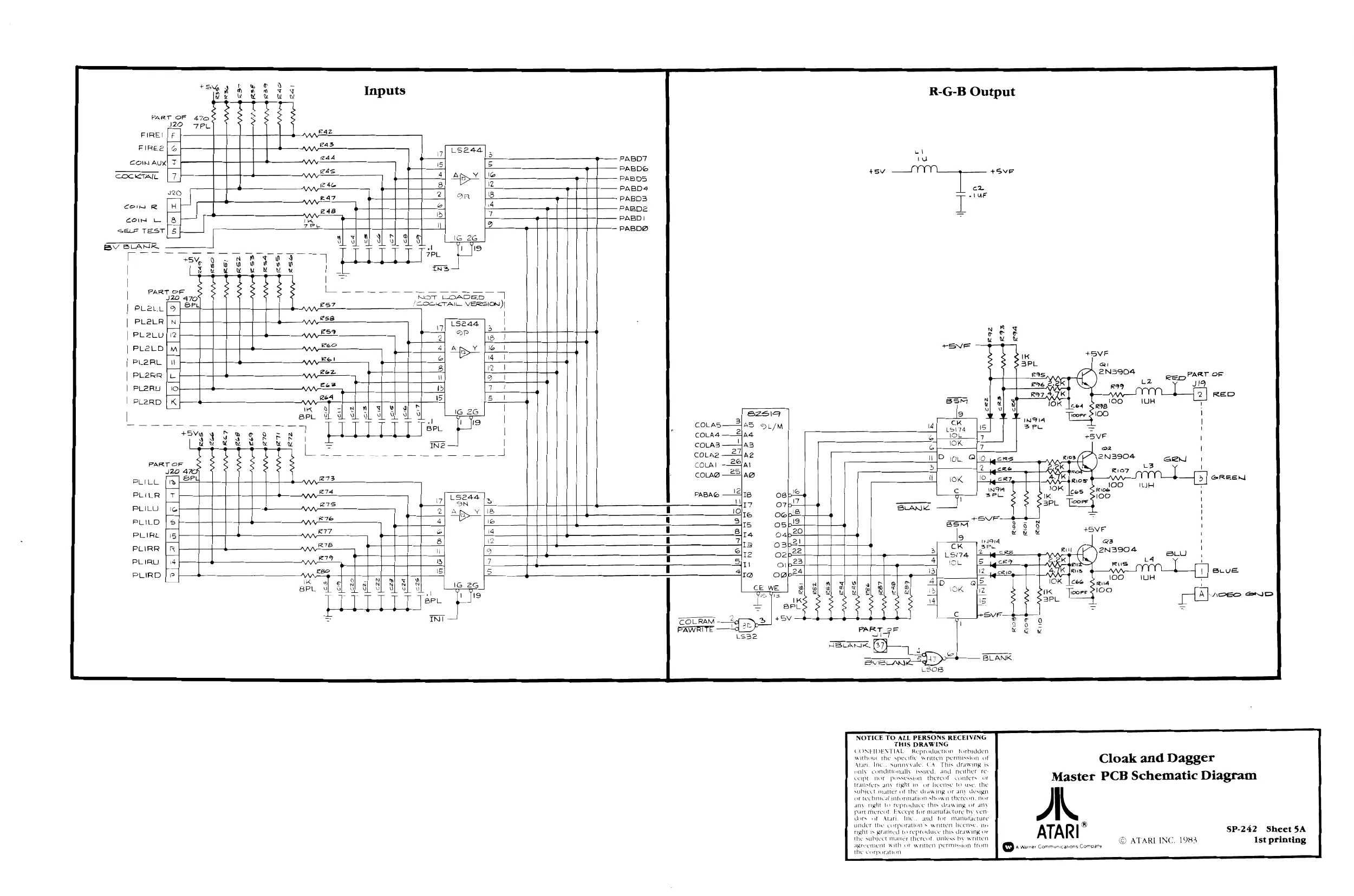
This page is a drawing, shown as the original scan.
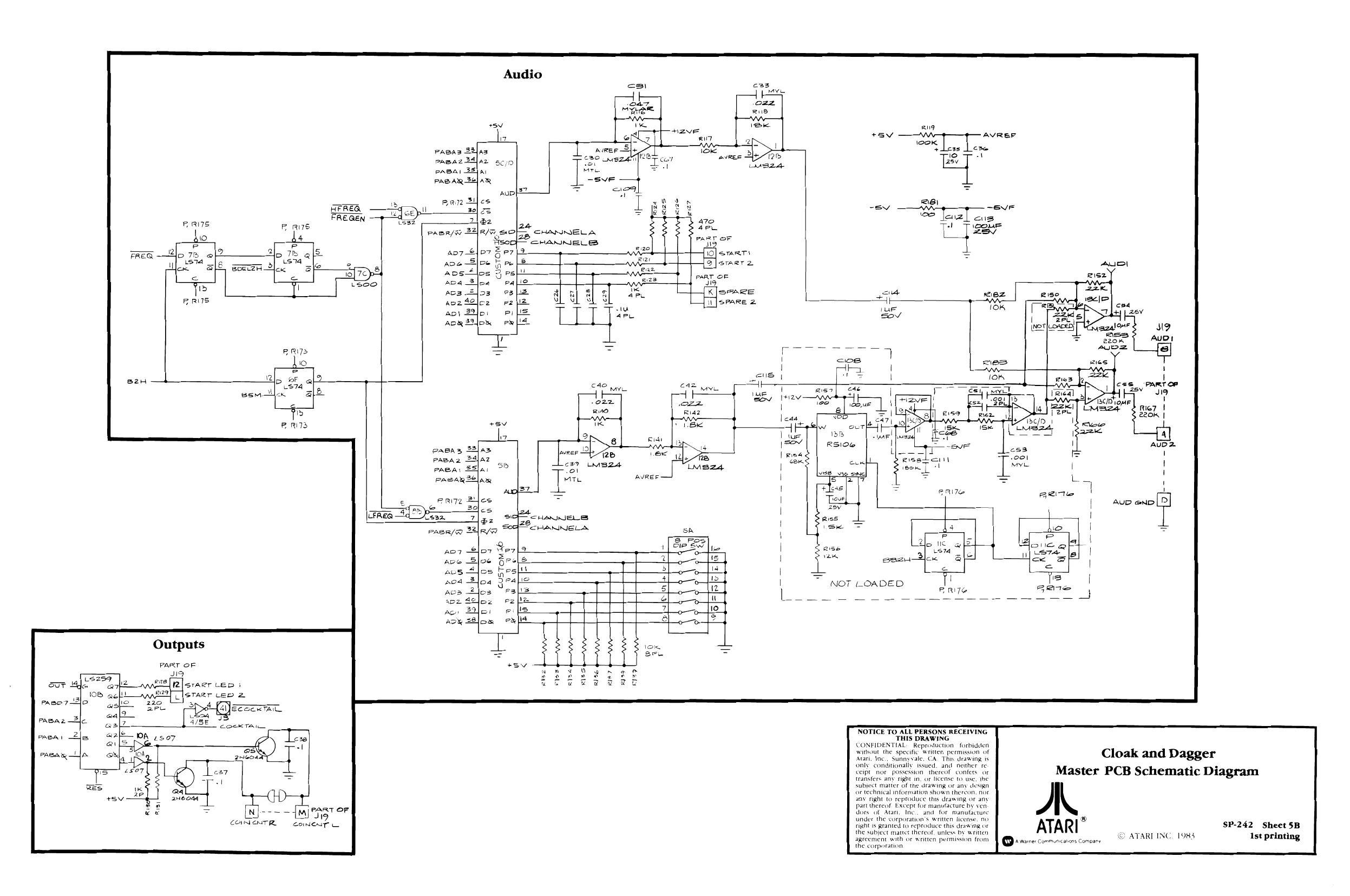
This page is a drawing, shown as the original scan.
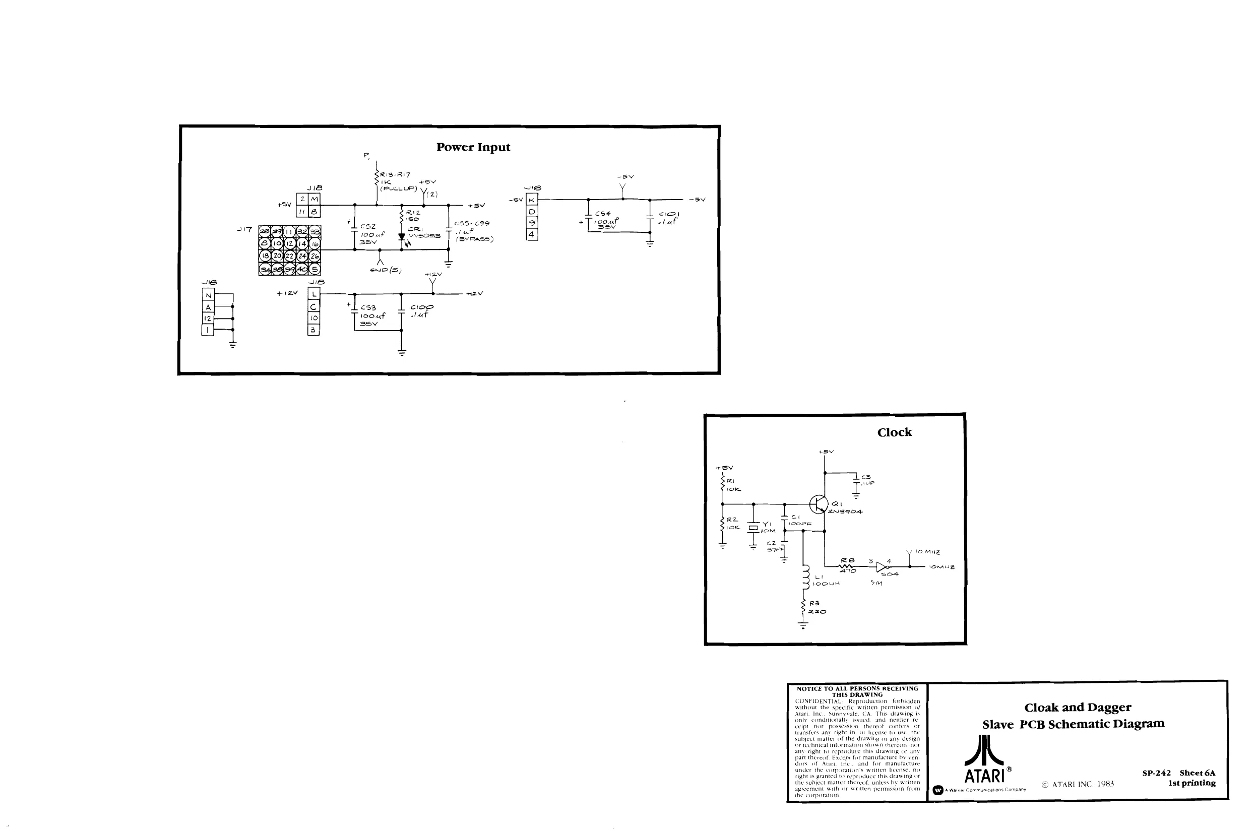
This page is a drawing, shown as the original scan.
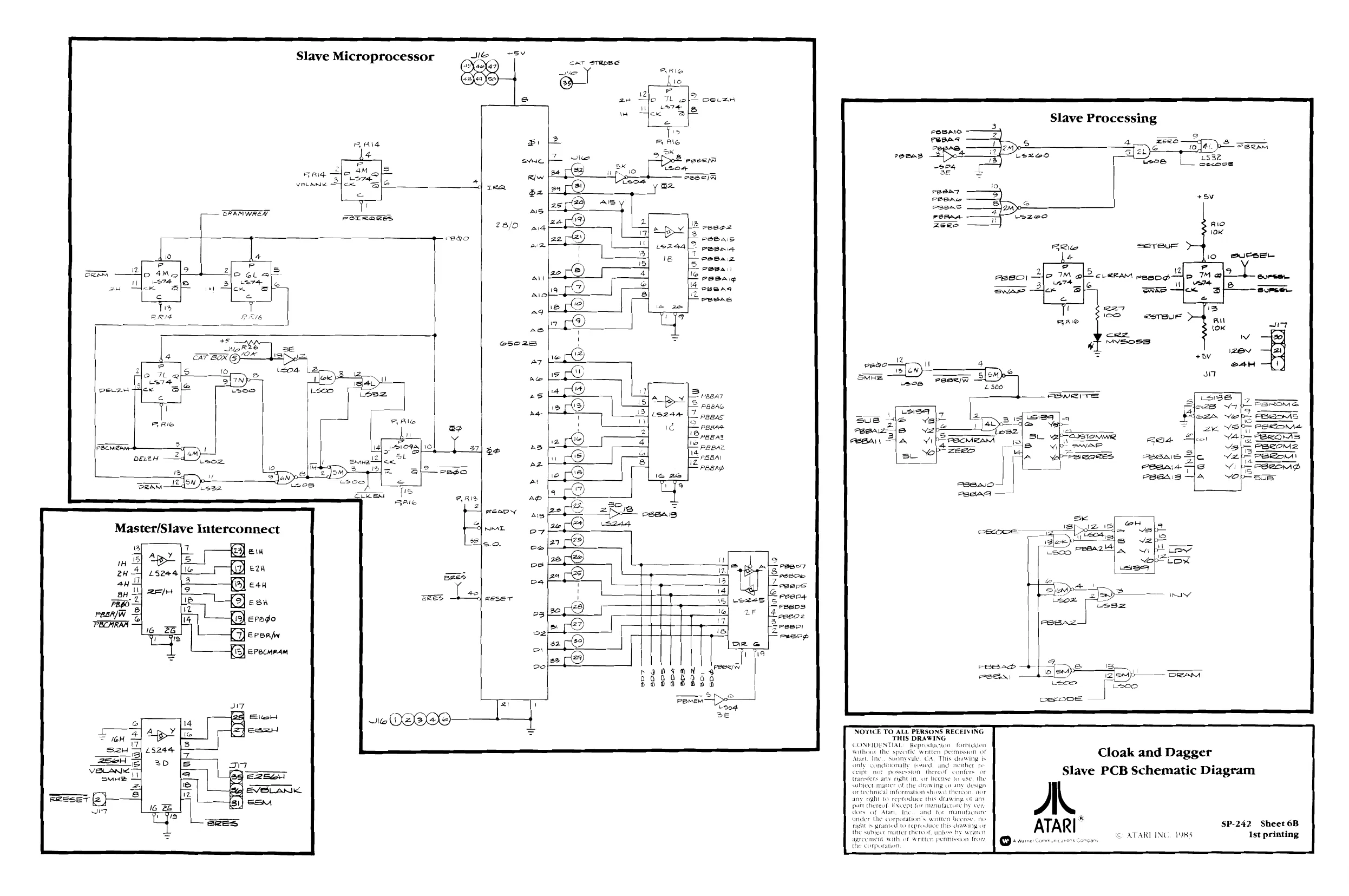
This page is a drawing, shown as the original scan.
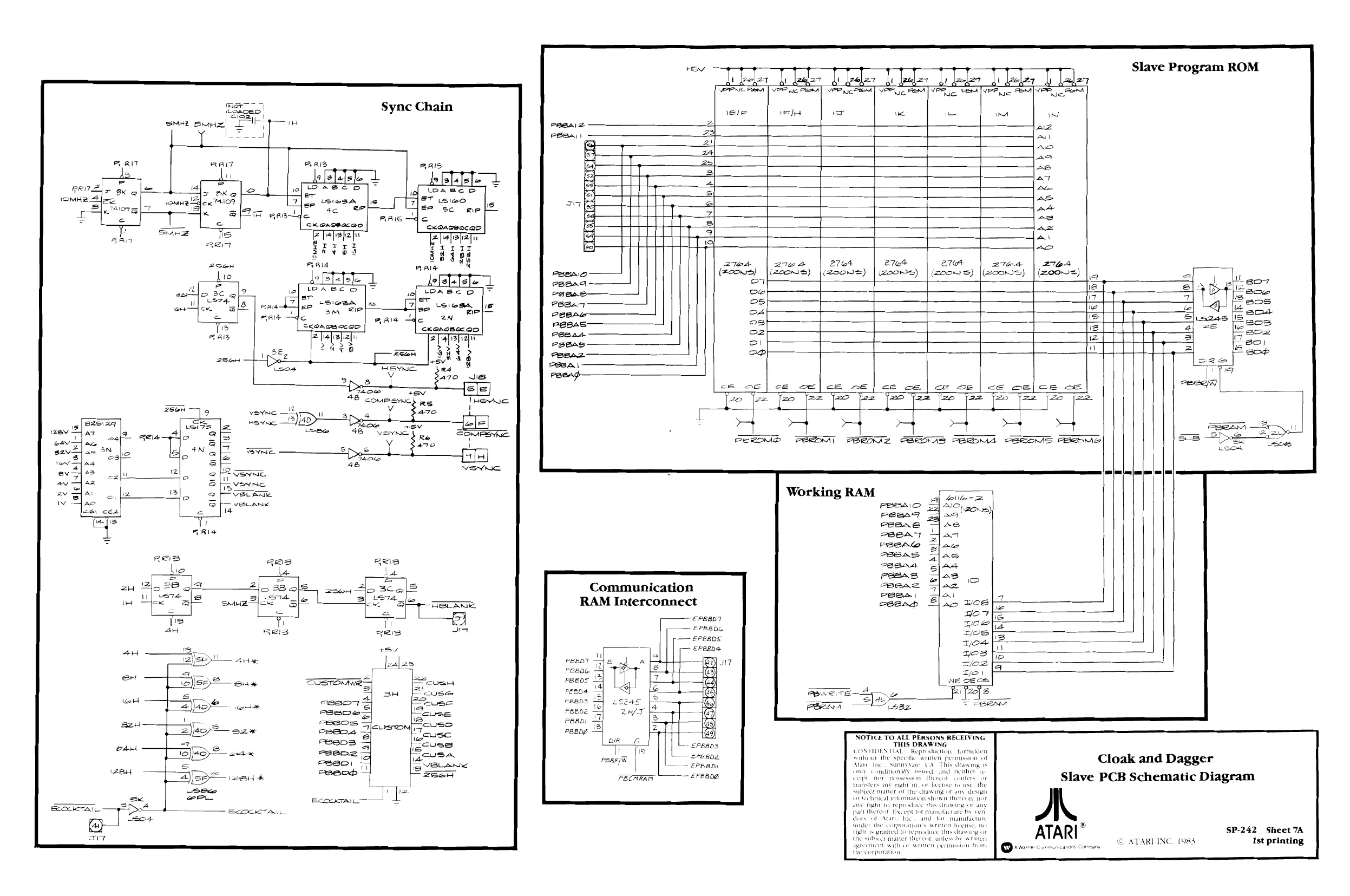
This page is a drawing, shown as the original scan.
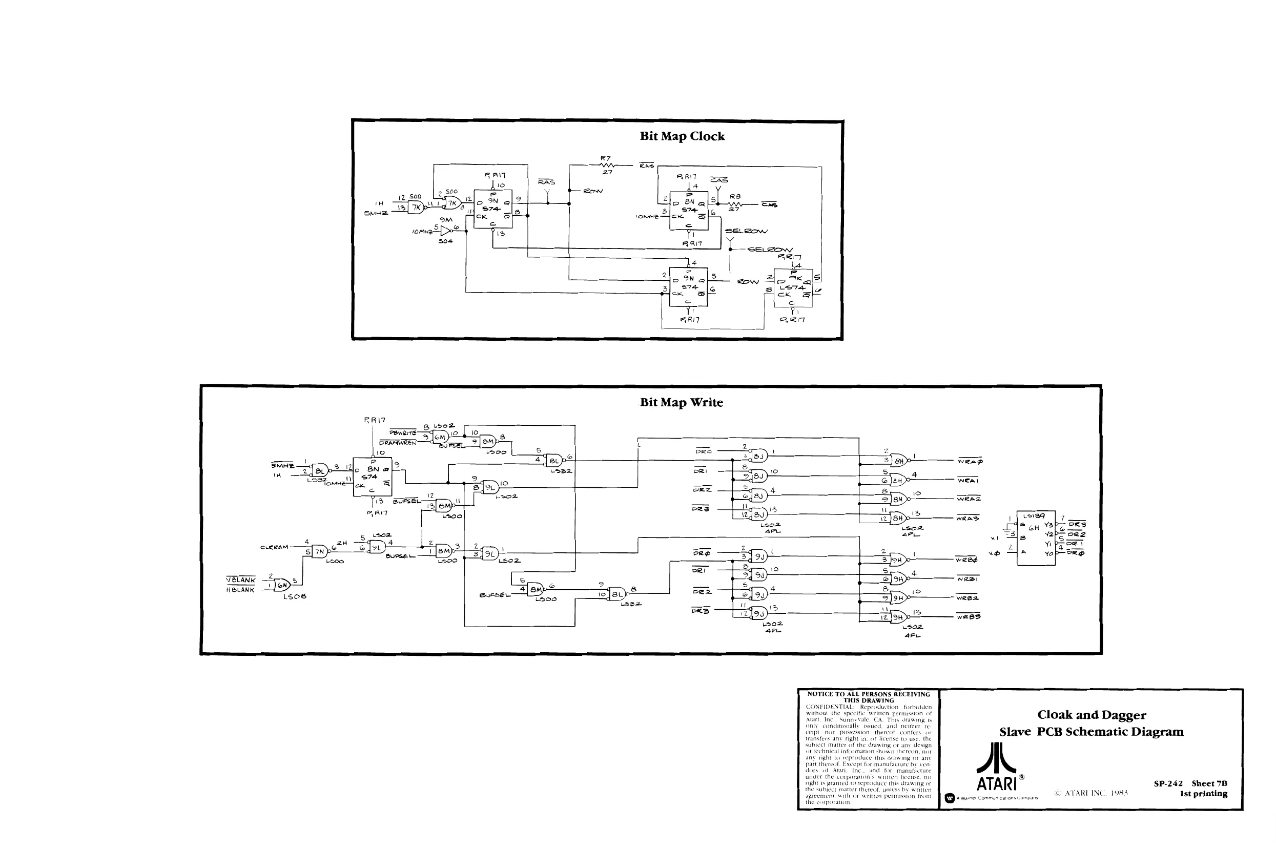
This page is a drawing, shown as the original scan.
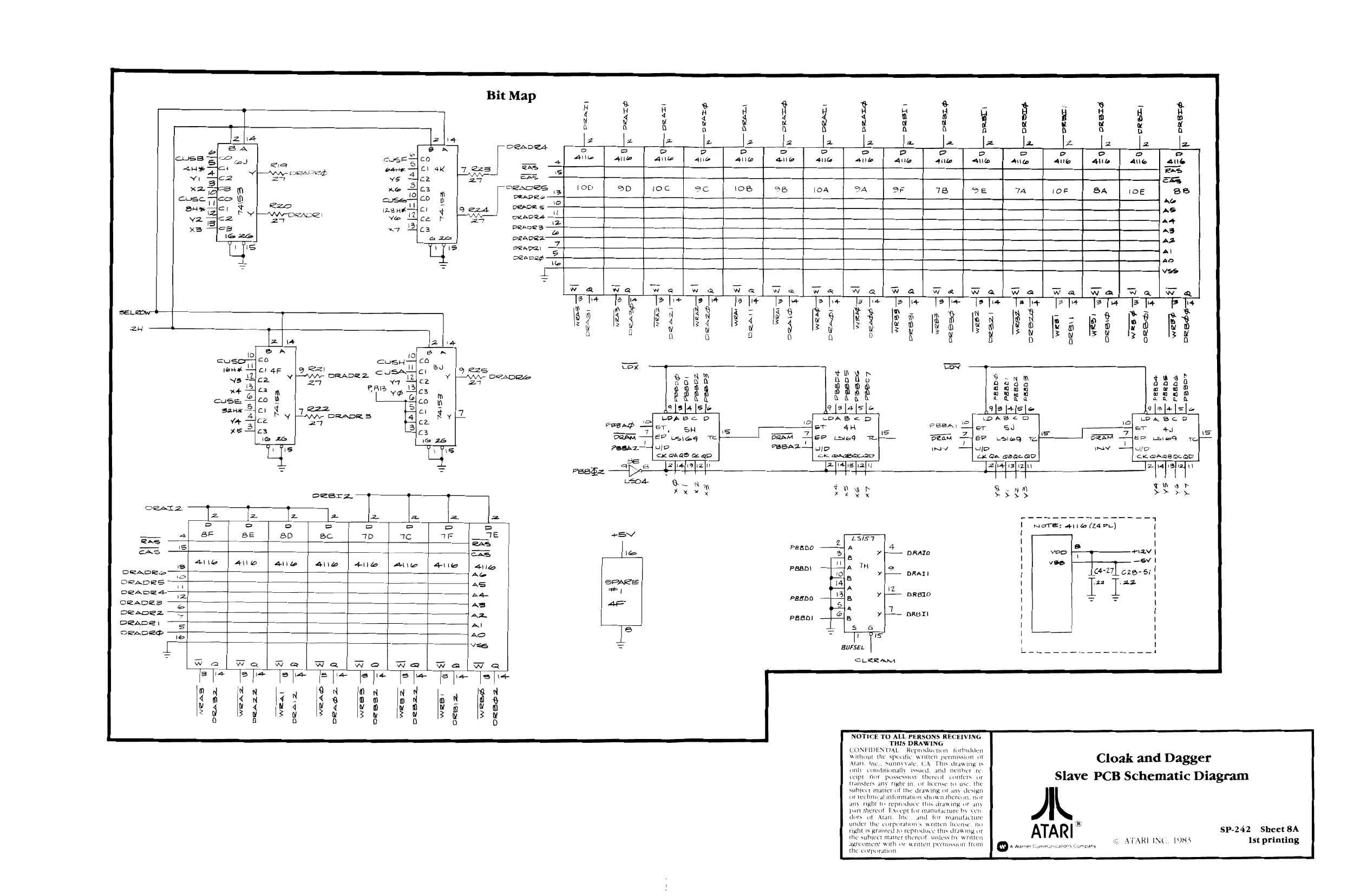
This page is a drawing, shown as the original scan.
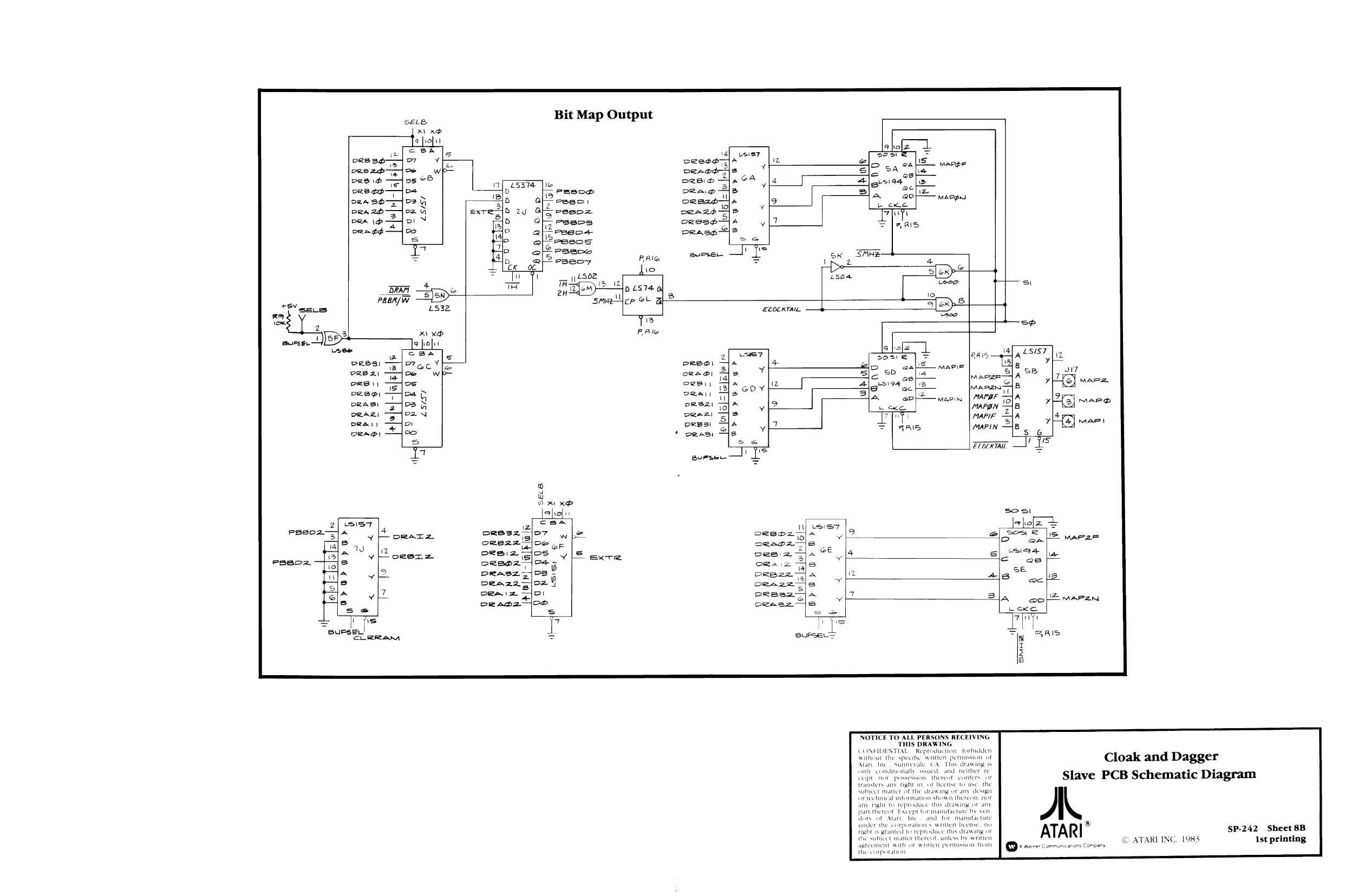
This page is a drawing, shown as the original scan.
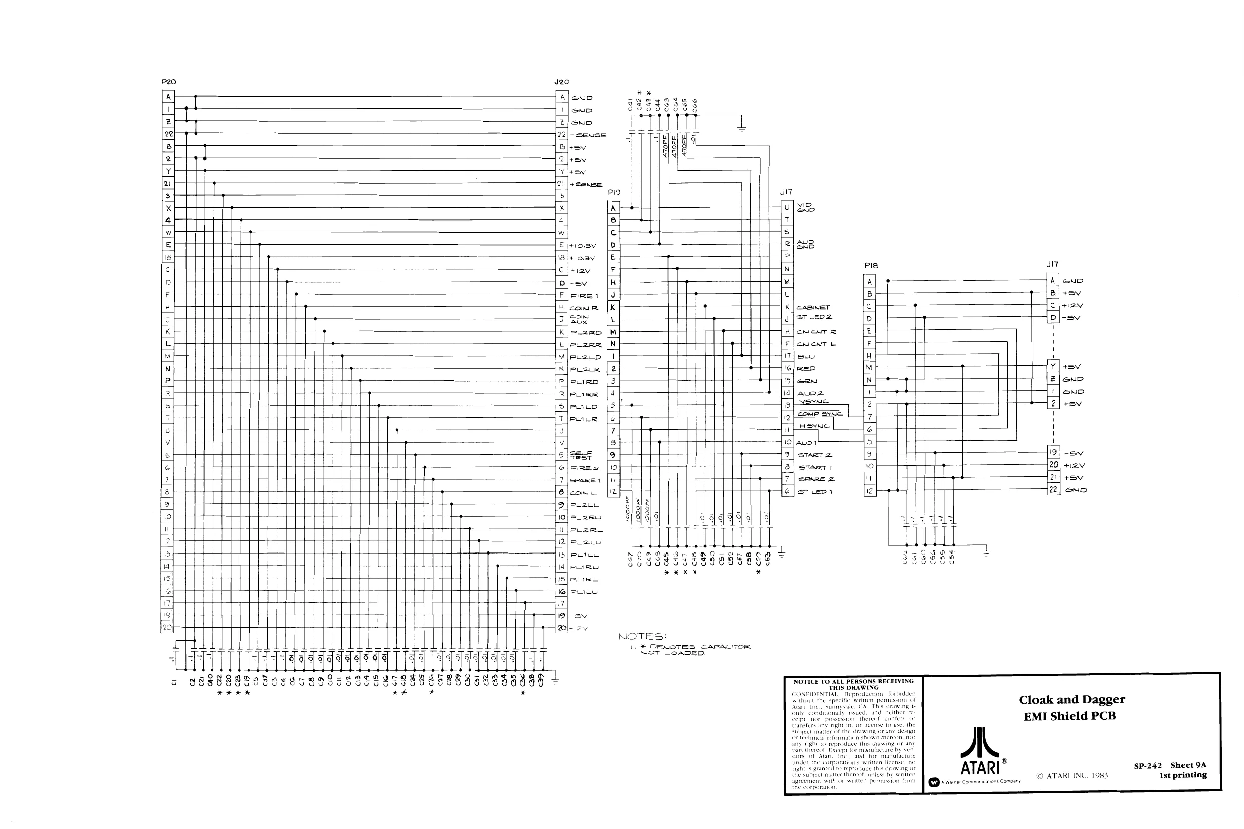
This page is a drawing, shown as the original scan.
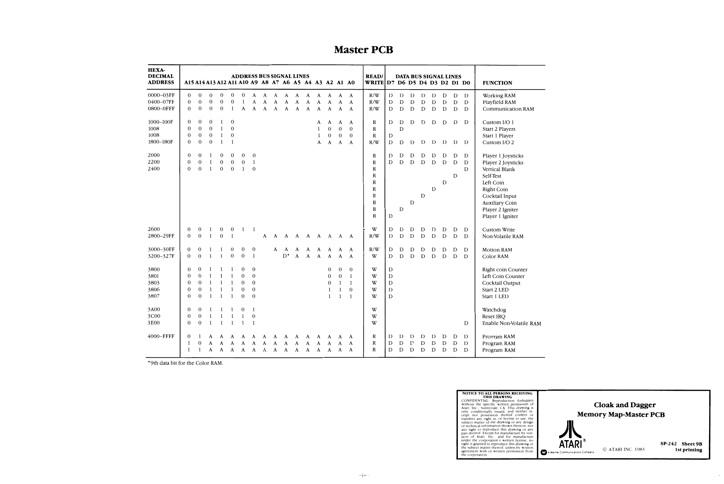
Master PCB
—_>———— HEXA- DECIMAL ADDRESS BUS SIGNAL LINES DATA BUS SIGNAL L) ADDRESS A15 A14A13 Al2 All A10 A9 A8 A7 A6 A5 A4 AZ A2 Al AO WRITE|D7 D6 D5 D4 D3 D2 D1 DO FUNCTION
| 0000-03FF | DD | bD»bD | DOD | OD | ~»D | Working RAM | ||
| 0400-07FF | DDDODODODOD | OD | Playfield RAM | |||||
| 0800-OFFF | DDoDODODODOD~OD | Communication RAM | ||||||
| 1000-100F | R | |D | DDODODoDoODOD | Custom 1/0 1 | ||||
| 1008 | R | D | Start 2 Players | |||||
| 1008 | R | D | Start 1 Player | |||||
| 1800-180F | RW | ITD | Db | DD | YD | D | iD | Custom I/O 2 |
| 2000 | R | DDoDODODODODOD | Player 1 Joysticks | |||||
| 2200 | R | DDODODODOD | OD | OD | Player 2 Joysticks | |||
| 2400 | R | D | Vertical Blank | |||||
| R | D | Self-Test |
R D Left Coin R D Right Coin
R D Cocktail Input R D Auxiliary Coin R D Player 2 Igniter R D Player 1 Igniter
| 2600 | DDDODODODODoD | Custom Write |
| 2800-29FF | DDODODODODODoD | NonVolatile RAM |
| 3000-30FF | DDoDoODODODODOD | Motion RAM |
| 3200-327F | DDbDODODODODOD | Color RAM |
| 3800 | D | Right coin Counter |
| 3801 | D | Left Coin Counter |
| 3803 | D | Cocktail Output |
| 3806 | D | Start 2 LED |
| 3807 | D | Start 1 LED |
3A00 Watchdog 300 Reset IRQ
| 3E00 | D | Enable Non-Volatile RAM | ||
| 4000-FFFF | DDD | DODD | ODD | Proeram RAM |
DDPDODODD»D Program RAM DDbDODODODOD~OD Program RAM
*9th data bit for the Color RAM
NOTICE TO ALL PERSONS RECEIVING "THIS DRAWING caer ene tame Joak and D: Auurt Inc. Sunmyvate. CA ‘ths Sawing Cloak and Dagger Ceipt “nor possession thereof confers or Memory Map-Master PCB transfers any right in, oF license to use, the subject matter of the drawing or any design
Or technical information shown thereon, nor
any right to reproduce this drawing or any part thereof Except for manufacture by ven: dors of Atari, Inc., and for manufacture fig is gramed to reproduce this drawing or ATARI ie SP-242 Sheet 9B the subject matter thereof, unless by written © ATARI INC. 1983 Ist printing
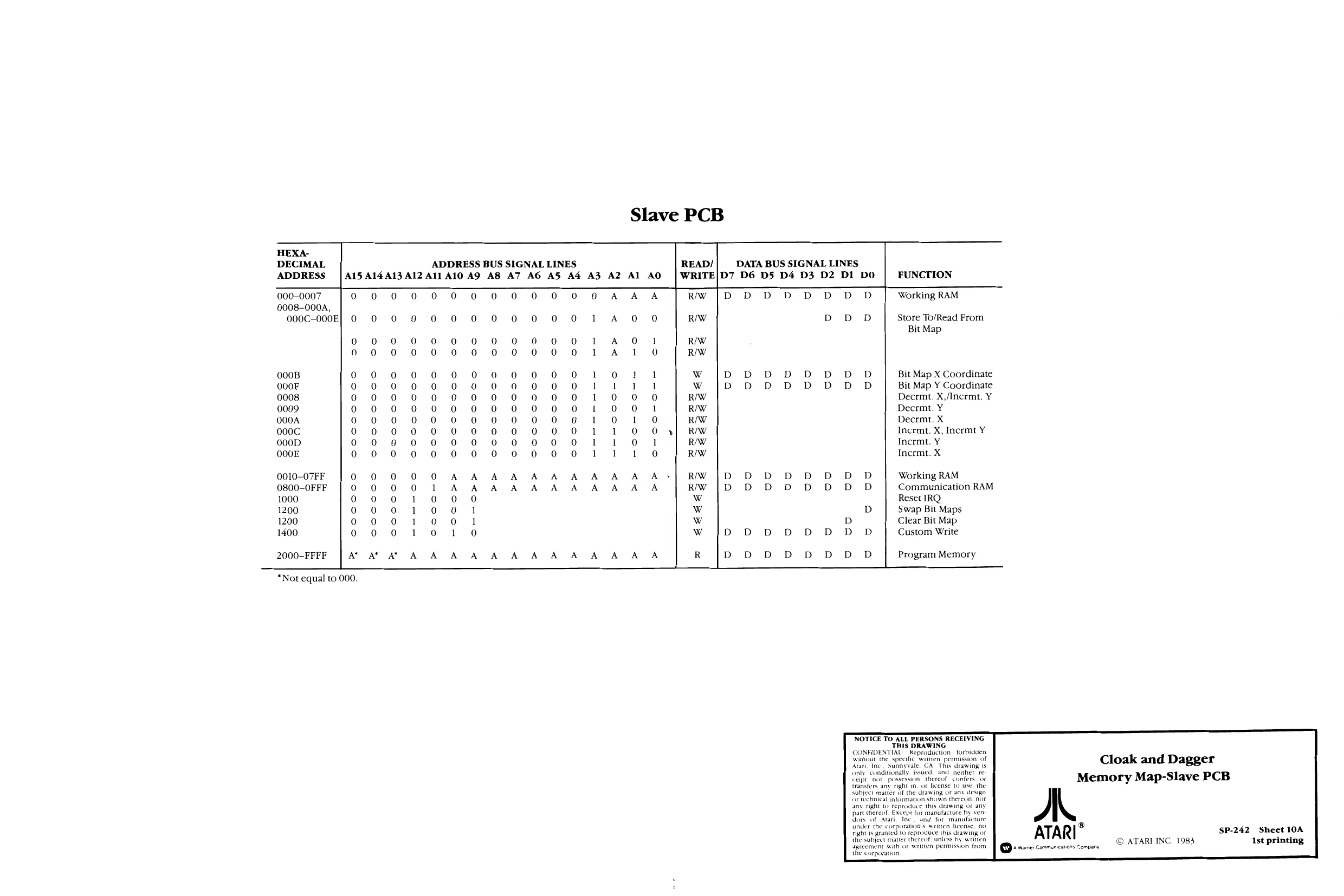
Slave PCB
HEXA- T
| DECIMAL | ADDRESS BUS SIGNAL LINES | READ/ | DATA BUS SIGNAL LINES. |
ADDRESS | A15 A14A13A12 All A10 A9 A8 A7 AG AS A4 A3 A2 Al AO | WRITE|D7 D6 D5 D4 D3 D2 D1 DO | FUNCTION
| 000-0007 | o 0 0 0 0 00 00 0 0 0 6 A A A | RW | DDD bDOD OD OD OD | Working RAM |
6008-000A,
| 000C-000E} | 0 0 0 6 0 0 000000 | 1 | 4 0 0 | RW | D D_ D_ | Store To/Read From |
Bit Map
| 0 0 | 0 | 000 00001aA 0141 | RW | |||||
| 9 0 0 0 0 00 0 0 0 0 0 | 1 | A | 1 | 0 | R/W | |||
| 000B | 0 0 00 0 0 0 0 0 0 0 0 | 1 | 0 | 1 | 1 | Ww | DDOD DOD DOD iD | Bit Map X Coordinate |
| O00F | 0 00000000000081tr1 | 1 | w | |D D DD D D D D | | BitMap Y Coordinate | |||
| 0008 | 000000000000 | 100 0 | RW | Decrmt. X,/Incrmt. Y | ||||
| 0099 | 0 0 0 0 0 00 00 0 0 0 | t | 0 0 | 1 | RW | Decrmt. Y | ||
| 000A, | 0 0 0 00 0 0 0 0 0 0 6 | 1 | ool | 0 | R/W | Decrmt. X | ||
| 000C | 0 000 00 00 0 0 0 0 | 1 | 1 | 0 0 yy] | RW | Incrmt. X, Incrmt Y | ||
| 000d. | 0 0 969 0 0 0 0 00 0 0 0 | 1 | 1 | 0 | 1 | RW | Incrmt. Y | |
| O00E | 0 0 0 0 0 0 0 0 0 0 0 0 | 1 | 1 | 1 | 0 | RW | Incrmt. X | |
| 0010-O7FF | 0 0 0 0 0 A A A A A A A A AAA | R/W | DDbDODODOD OD iD | Working RAM | ||||
| 0800-OFFF | o 0 0 0 | 1 | A A A A A A A A A A A | R/W | DD DoDD DD D | Communication RAM | ||
| 1000, | 0 0 0 | 1 | 0 0 0 | Ww | Reset IRQ | |||
| 1200 | 00010041 | w | D_ | Swap Bit Maps | |||||
| 1200 | 0 0 0 | 1 | 0 0 | 1 | Ww | D | Clear Bit Map | |
| 1400 | 0 0 0 | 1 0 | 1 | 0 | Ww | DDobDODODODOD YD | Custom Write | |
| 2000-FFFF | Av At AT A OA | A A A A A A A A A A | R | DD ODODODODOD D | Program Memory |
*Not equal to 000.
NOTICE TO ALL PERSONS RECEIVING THIS DRAWING CONFIDENTIAL: Reproduction forbidden Seimhout the specific writen permission of Cloak and Dagger Aun. Inc. Sunnyvale, CA This. drawing. is cab ‘hor pomession thereat Contes Memory Map-Slave PCB transfers any right in, oF license t use the subject matter of the drawing or any design br technical information shown thereon, nor any right to feproduce this drawing or any part thereof Except for manufacture by ven. dors of Atari, Ine. and for manufacture under the corporation's weiten license. 90 ATARI ® SP-242 Sheet 10A Sarcemenr wih ce wenten permsion fm) | Qawuresconmancsionsconoany © ATARI INC. 1983 Ist printing the corporation
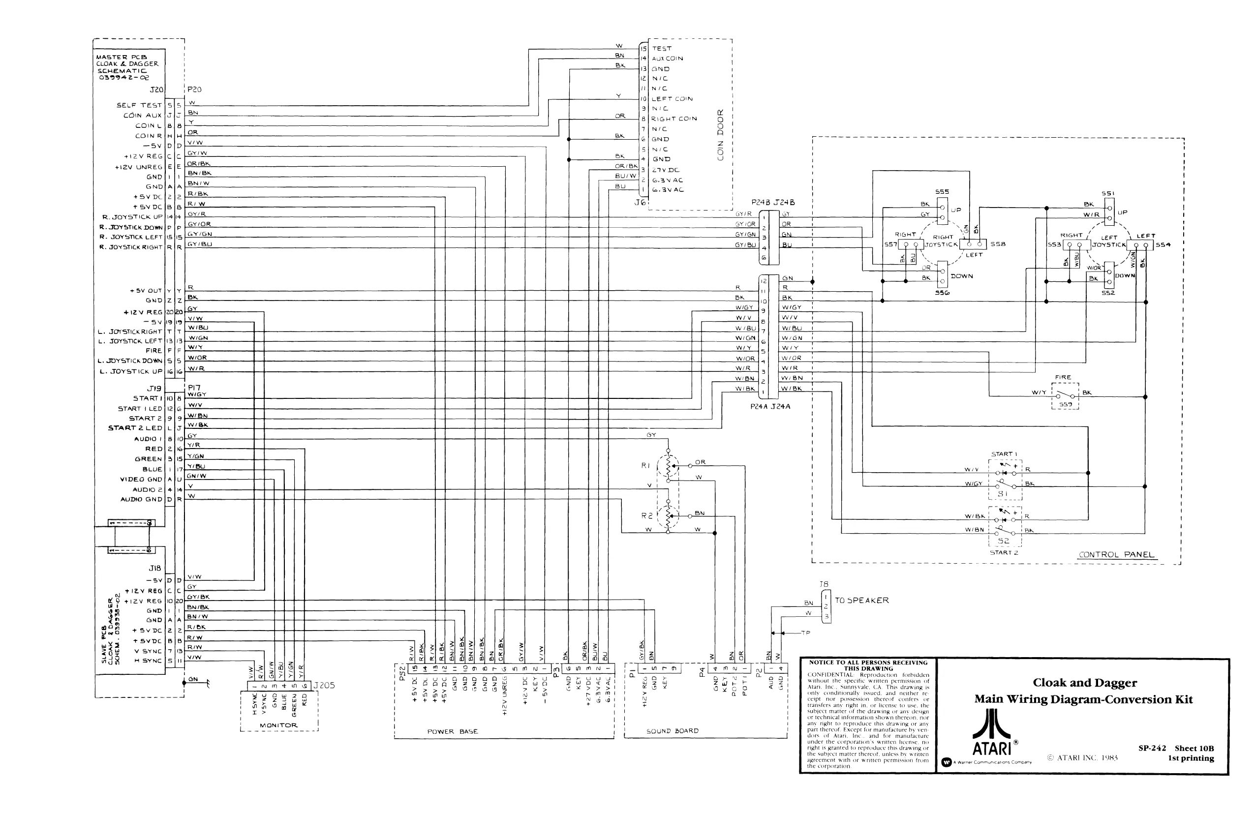
This page is a drawing, shown as the original scan.