Midway Standard Test Procedures for Processor Boards (M1700-1 July 1976)
Midway Processor Boards (Midway MFG. CO., 1976) · Manual · 55 pages · 39 sections · original scan
MM 4700-1
STANDARDIZED
TEST PROCEDURE
FOR ;
MIDWAY’S PROCESSOR BOARDS
uf
MIDWAY MFG. CO. 10750 WEST GRAND AVENUE FRANKLIN PARK, ILLINOIS, 60131, U.S.A. PHONE: 312 451-1360 TOLL FREE NO.: 800 323-7182
CABLE ADDRESS: MIDCO TELEX NO: 72-1596
FLOW CHART OF TROUBLESHOOTING
PROCEDURE
BAD BOARD
GQ TO CASE C
REMOVE PROM H
GO TO CASE B3 GO TO CASE D
BAD VERTICAL LINES PERFORM
GO TO CASE B2
GOOD BOARD
STANDARDIZED TEST PROCEDURE
FOR
MIDWAY’S
PROCESSOR BOARDS
TABLE OF CONTENTS
Flow Chart of Troubleshooting Procedure . . Inside Front Cover
ii List of Illustrations . . . 1... eee ee ee ee ew ww tt
- INTRODUCTION. ©. 2. 1 we ee ee ee ee ee ee ee ee ee ed
- ASSUMPTIONS . . 2... . . ee ee ee ee ee ee?
- TEST PROCEDURE. ~. 2. ee eee ee ee ee ee ee 8
3.1 Preliminary Instructions .........-6 +e. ee. 03
3.2 Case A: Good Picture - Bad Program. .........-5
3.3 Case B: Bad Picture... .... 2... ee eee ee eT
3.3.1 Case Bl: Good Vertical Lines... .......7
No Ram Test... 6. e- e ee ee ee Dd
3.3.2 Case B2: Bad Vertical Lines. ......... 15
3.3.3 Case B3: No Vertical Lines... .... 2... 23
3.4 Case C: No Picture - Dead... ... ee... es. 32
3.5 Case D: Bad Cowboy... . . 1 ee eee eee ew es 36
Lines in Cowboy... 1... eve ee eee 37
Sample. . 1. wwe ee ee ee ew 8
- APPENDIX 1: Clock Section Check. ........... =. 40
2: Some Useful Pin Configurations and Logic Diagrams. .........24..... 44
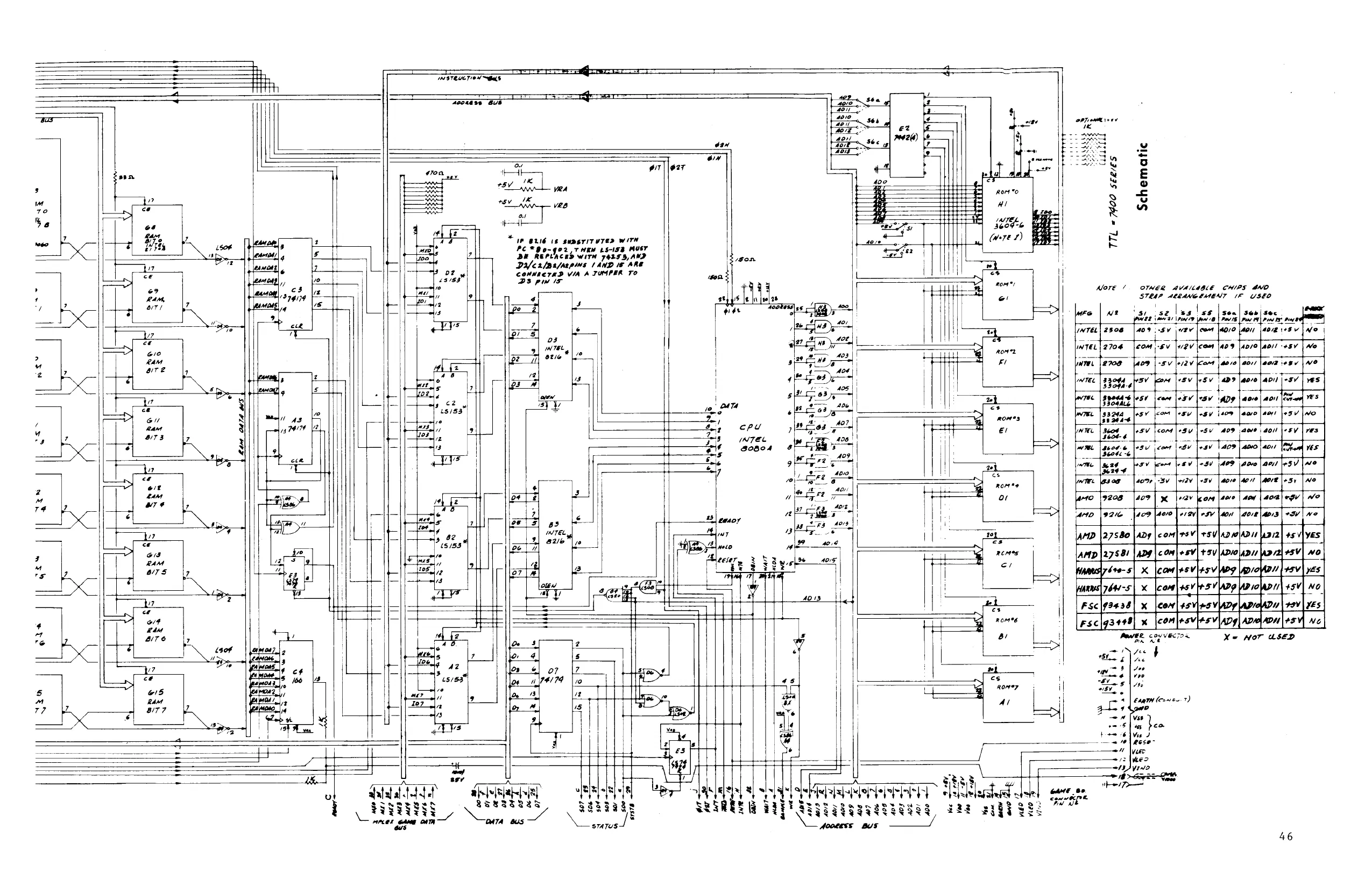
3: Mother Board Schematic. ........... 46
3.3.1-1
3.3,.1-2
3.3.1-3
3.3.1-4
3.3.1-5
3.3.2-1
3.3.2-2
3.3.2-3 Good LIST OF ILLUSTRATIONS
Picture with Good Program
Gunfight
Sea Wolf
Vertical Lines.
Section showing PROMS and IC 7442.
Section showing IC 74174's
Waveform at C3 PIN 2
Ram Address. . ..
(a)
(b)
Section showing Inputs to RAMS
Good
Good
(a)
(b) With Information
Without Information
Tri-State Data Input,
Ram Data Output
Tri-State
Bi-State
di li
Figure #
3.3.2-4
3.3.2-5
3.3.2-6
3.3.2-7
3.3.2-8
3.3.2-9
3.3.3-1
3.3.3-2
3.3.3-3
3.3.3-4
343-35
3.3.3-6
3.3.3-7
3.3.4-1
3.3.5-1
3.3,5-2 List of Illustrations
(cont.)
Good Address - . 6 1 ewe ee ee eee
Section showing Bidirectional Lines. ......
Input from Multiplexer to IC 8216. .......
Bidirectional Line - - - +--+ 6 ee ee ee eee
Clock at Pin 2 of Multiplexer IC 74153... .
Clock at Pin 14 of Multiplexer IC 74153.
Section showing Clock Driver Inputs and Outputs
Clock Driver IC 3245 Outputs. .--+.....
Flip Flop IC 74L8S74 at EX «© «© «© e+ ee ee eee
Section showing Inputs and Outputs of IC 9322 at
Sync, WR, and DBIN at CPU + + + «+ ee ewe
Ram Write Enable - Pin 12 of RAMS -
Section showing IC 74LS74 at E3 and part of Associated Loop,
Pin 15 of IC 74166 at C4,
Sample... ... ee. eae
Section showing Sample. . .
iii F4.
Chapter 1
INTRODUCTION
The tremendous success of Midway's Gunfight and Sea Wolf games
in the coin-operated amusement industry has created a new kind of
need. This need has been felt because of the deviation from the
usual TTL and the advancement into the Microprocessor (CPU) and
the associated circuitry involving RAMS and PROMS. Much has been
said and talked about regarding the CPU, RAMS, and PROMS both in
the literature and outside, but little has been said or done about
troubleshooting a board using these. Hence, this book has been
specifically tailored to meet the requirements of troubleshooting
Midway's Processor Boards*, (henceforth - referred to as Mother
Boards). It does not in any way try to explain how the board
works. Throughout the book the major emphasis has been on "How
to Fix the Board" and no attempt has been made to describe "How
it Works".
The Mother Boards used in both the games Gunfight and Sea
Wolf are identical except for the Program part. However, to fa-
cilitate the writing of this book reference has been made to the
Gunfight game. Substituting "Ship" for "Cowboy" in this book
should enable fixing the Sea Wolf games as well.
- The turnout percentage of these boards at Midway Mfg. Co. is of the order of 99.7%. This relatively small fall-out is mainly attributed to the manufacturing defects of boards and not the troubleshooting procedures used!
Chapter 2
ASSUMPTIONS
- It is assumed that the Mother Board was working once and
has gone bad during use, that is, there are no shorts on the board.
However, instances where shorts could exist and cause grave pro-
blems have been taken into consideration.
- It is assumed that (a) the Power Supply, (b) the Game
Board, and (c) the Tester are all in good working condition. Also
the Monitor is synchronized.
- It is assumed that the Operator has the following avail-
able:
- A 50 MHz Oscilloscope
- A Ram Test Board with a good Test PROM (GUN FIGHT & SEA WOLF ONLY)
- A set of good ROMS or PROMS
Chapter 3
TEST PROCEDURE
3.1 PRELIMINARY INSTRUCTIONS:
- Make
hanging jumper
- Make
Board is tight
- Make sure the Mother Board looks physically OK - no
wires or burnt out chips.
sure that the jack from the Tester to the Mother
and properly connected.
sure the Game Board fits into the Mother Board jack
tight. It is not necessary to hook up the Game Board jacks from
the Tester at this time. Remember that without the Game Board or
Ram Test Board in the Mother Board jack the CPU would not operate.
The main criteria here is that "Hold" (pin 13 of CPU) should be
low.
- Turn on the Power Supply switch.
- Check the following: +5V, -5V, +12V, VRAYAt5V, VRBieatSV.
(L£ VRA or VRB
If it is still is low cut out the 0.1 MF Capacitor near A3 and A5.
low refer to Case C, Step 3).
- Make sure that CPU socket is not broken and the PROMS are
not loose in their sockets.
- What is seen on the screen would naturally vary from
board to board. Each of these is discussed separetely. Proceed
to the relevant case.
3.2 CASE A: GOOD PICTURE - BAD PROGRAM
By good picture is meant here a clear screen with the words
"Game Over" and "0" on either side of it. In the case of a good
Mother Board the words "Gun Fight" would be seen followed by the
Cowboy coming in, shooting a bullet downwards, and walking back.
During this process the words "Insert Coin" would appear on the
lower right hand side temporarily (Figure 3.2-1). If all or part
of this is bad it could most likely be a program problem.
GUN FIGHT SEA WOLF
&
INSERT COIN
INSERT COIN HIGH SCORE ooo
- Gunfight (b) Sea Wolf
Figure 3.2-1 Good Picture with Good Program
Try changing the PROMS one at a time till it is rectified. If the
program seems alright and the Cowboy shape or movement is bad go
to Case D.
If the above checks OK hook up the Game Board jacks and play
the game. If the game cannot be played correctly (e.g. picture
breaks down when one Cowboy shoots another, other characters in-
stead of numericals appear at time count, etc.,) then the problem
could most probably be in the PROMS. Try changing them one at a
time.
In some instances it is a good idea to check the Ram Test out
all the way. Though the Ram Test should be expected to work this
is a good procedure and is recommended here.
3.3 CASE B: BAD PICTURE
When the words "Game Over" are not seen on the screen and
the screen is filled with a lot of irrelevant, unitended material
(Garbage) it is referred to here as bad picture. When the Mother
Board gives a bad picture the first step would be to remove the
PROM H from its socket. When PROM H is removed the screen should
normally display good vertical lines (Figure 3.3.1-1). In some in-
stances, however, the vertical
lines may be present but bad, or there may not be any vertical { | lines at all. It is suggested |
that all the PROMS be removed
at this time. Depending on the
pattern displayed on the screen
go to the relevant section
Figure 3.3.1-1 Good Vertical Lines
3.3.1 CASE Bl - GOOD VERTICAL LINES: The vertical lines are said
to be good when there are sixteen clean vertical columns on the
screen. Each column consists of 16 lines. Only 4 of these are ON
at a time and these are arranged in the following order: 1 line
on, 2 lines off, 3 lines on, and 10 lines off. If the vertical
lines are good hit the tilt (Reset) switch till the pattern shifts
on the screen. If the second pattern is also good it means that
the CPU and RAMS are most probably working well. If one or more
of these lines are bad or displaying dots on screen possibly the
problem rests in the RAMS, then to to Case B2.
FIGURE # 3.3.]-2: SECTION SHOWING PROMS AND IC 7442
OPTIONAL 1K , +5V
oO snd NOILONULSNI
EOS OP 07 ssaadqy mi
sna ssauqqy
If the vertical lines check good perform the Ram Test. (If the
Mother Board use& 8K ROMS all of them should be removed to per-
form the Ram Test). If the Ram Test stops after a few scans the
board would read out the bad RAM which should be changed. If the
Ram Test runs all the way the problem rests with the program. The
PROMS should be changed one at a time to get a good picture. Of
course, PROM H should also be inserted at this time. Even after
changing all the PROMS if the picture is still bad then it means
that there is a break on the lines leading to the sockets. The
best thing to do at a time like this is to remove all the PROMS
and check all the pins for continuity (Figure 3.3.1-2). Generally
the problem should be isolated by this time. If not, specifically
check all the pins on IC 7442 at E2. There should be high fre-
quency pulses on all pins 1 through 9 except 8 which is ground.
(In the case of boards using IC 3205 in place of IC 7442 the
corresponding pins are 7 and 9 thru 15).
NO RAM TEST
A number of causes could result in a No Ram Test situation.
The following hints should however be helpful:
- Make sure that the ID lines reach the PROM H socket (pins
9, 10, 11, and 13 thru 17) and are not short to one another. This
could be done by grounding one at a time and checking the others
with a scope. On Mother Baards using 8K ROMS the lines should be
floating and on those using 4K PROMS the lines should be high.
FIGURE # 3:3.]-3: SECTION SHOWING IC 74]74s8
RAM DA 6
RAM DA 7
RAM DATA BUS
FROM a4 PIN 8
FROM B4 TO A4 PIN
PIN 10,13
- If the ID lines check OK, and they should on most boards
that were working before, with the TEST PROM Cable removed check
the outputs (Figure 3.3.1-3) of the IC 74174's at A3 (pins 2 and 5)
and C3 (pins 2, 5, 7, 10, 12, and 15). Pins 2 and 5 on A3 and pins
5 and 7 on C3 should be low and there should be pulses on all the
rest (Figure 3.3.1-4). If this condition is not met follow the
line backwards to isolate the problem. A good trick at this point
would be to ground these pins
one at a time and hit the tilt
(Reset) switch to see if it
starts the Ram Test. IF it
does it would stop after 1 scan.
This would indicate that the
problem is on that line. Follow
it backwards and check all pins
on the corresponding pair of Figure 3.3.1-4 Waveform at C3 Pin 2 RAMS. Change the correspond- Vert: 1V/div, Horz: 2p Sec/div
ing IC 74174 if necessary.
ll
- IF 1 and 2 do not locate the problem check the RAM
Addresses (Ram Ads) going to the RAMS for shorts and/or breaks.
It is generally sufficient to check all pins on H8, G8, H15, G15.
If any of the Ram Ads look fishy check the inputs to the corres-
ponding IC 9322 or IC 74157 at F4, F5, F6, or F7. (Figure 3.3.1-5).
If necessary change the chip.
- If the Ram Test board reads out a RAM as bad check all
pins on that RAM before changing it. The Ram Test board generally
helps to narrow down the problem area.
- With Information (b) Without Information
Figure 3.3.1-5 Ram Address Vert: 1V/div, Horz: 0.5 p Sec/div
- In some instances the Multiplexers (IC 74153's) could
go bad and cause the No Ram Test situation. This could be
verified as follows: Check the output pins 7 and 9 on A2, B2,
C2, and D2. There should be pulses on all of them (Figure 3.3.2-6).
Now ground the corresponding ID inputs (pins 4 and 12) of each
of these outputs and observe them. All the outputs except pins 7
and 9 of D2 and 7 of C2 should go low when the corresponding ID
lines are low. On these three, however, there would be some ob-
vious change in pulse duration and frequency. If any of the
IC 74153's does not behave as described above it should be changed.
FIGURE # 3.3.2-1:
RAM ADDRESS BUS
SECTION SHOWING
RAM INPUTS
3.3.2 CASE B2 - BAD VERTICAL LINES: By bad vertical lines what
is meant here is that the vertical lines are present but there is
"garbage" associated with it. The "garbage" basically is of three
types. Type 1: In the form of dots scattered and/or uniformly
distributed across the screen. Type 2: In the form of rectangular
blocks running horizontally across the screen. Type 3: ({n the
form of rectangular blocks running vertically on the screen. Type
1 is attributed to bad RAMS or missing Ram Address to the RAMS,
Type 2 to a bad address line/s, and Type 3 to bad data line/s.
TYPE 1
When the problem is of this type the first thing to check
would be the Ram Ads on all RAMS. As mentioned earlier it is
generally sufficient to check all pins on H8, G8, H15, and G15
(Figure 3.3.2-1).
A typical Data Input to
the RAMS and RAM outputs
(both Bi-State and Tri-
State) are provided in
Figure 3.3.2-2, and
Figure 3.3.2-3 respec-
tively.
To identify the
RAMS causing the dots
on the screen try the Figure 3.3.2-2 Good Data Input (Tri-State) Ram Test first. If Vert: lV/div, Horz: 1 p Sec/div
the test starts it
would stop at the dot and the board would read out the bad RAM.
- Tri-State (b) Bi-State
Figure 3.3.2-3 Good RAM Data Output Vert: 1V/div, Horz: 1p Sec/div
If the test does not start and still the board reads out a RAM
as bad go to the output of that RAM (pin 7) and ground it. This
would verify the board by putting a white line through the dot.
Change all RAMS necessary till the Ram Test runs all the way.
Slightly adjusting the potentiometer (pot) of the +5V supply also
helps in locating bad RAMS. If the board does not read out any-
thing go to the inverters IC 74LS04 or IC 7404 at D4 and E4 and
ground them out one at a time till it either takes the dots out
or puts a line through them. This would naturally identify the
pair of RAMS that could be bad. Check all pins on these RAMS for
breaks, and the data input (pin 6) and output (pin 7) before chang-
ing them.
It has been observed that a bad Clock Driver (IC 3245) at C5
could cause dots on the screen. It is advisable to check this
out by freezing or heating it as required and changing it if ne-
cessary.
In rare instances the IC 74LS08 at F3 could also cause dots.
This could also be checked by freezing and heating as required.
- It is very easy to make solder shorts or break lines when changing RAMS. So it is a good idea to exercise great care and check for shorts and/or breaks everytime a RAM is changed.
TYPE 2
When the address line/s are bad check all the inputs and out-
puts of the IC 74LS08's at G3, H3, F2, and F3. See Figure 3.3.2-4
for a sample of an address. It has been observed that this section
has practically never caused any
problems and hence is not em-
phasized here.
Figure 3.3.2-4 Good Address Vert: ly/div, Horz: 2 p Sec/div
NOTES
This space is provided for personal notes
MIDWAY MFG. CO.
TYPE 3
When the data lines are bad check all the pins of the Bus
Drivers IC 8216's at B3 and D3 (Figure 3.3.2-5). Figure 3.3.2-6
shows the input, Figure 3.3.2-7 shows the bidirectional line from
the CPU and Figure 3,3.2-2 shows the output of the IC 8216.
Figure 3.3.2-6 Input from Figure 3.3.2-7 MUX to 8216 Vert: 1V/div, Vert: Ilv/div, Horz: 2p Sec/div Horz: 2p Sec/div Bidirectional Line
FIGURE # 3.3.2-5: SECTION SHOWING BIDIRECTIONAL LINES
FROM C5 FROM C5 PIN 10 PIN |5
150 150 OHM OHM > 2 BBS [+ J+
22 5] 2 o] 28
| 4 | vy | 0 125 |
2 ADDRESS DO J [26
2 2
DI 2 0 3 | 29
D2 2 4 QO
4 un
| D3 | a | 5 13 |
a a = 6 o,| DATA & 9 oO Qyh 1 ° 7 133 2 o
n 4
| D | 4 fa | 8 134 |
a 5 g
| é | 7 8 | 9 |
Pa D
| a) | a | a |
aq Jo 3 4 6 4 Ji [40
| pa | 7 | y2 [37 |
4 H 5 a 3 g
| ps | = READY | : |
| uu | Se) ry | 14 |g |
3 135} HOLD Sy 15 | ge 4 RESET D7 9 To] [6 J 17 papiyis > x =
SYNC
INTE
DBIN
WAIT
HLDA
If the problem is found to be difficult to isolate it often
helps to cut out the input pins 4, 7, 9, and 12 of the IC 8216's
one at a time. Each time hit the Reset switch. If this helps
follow that line backwards to the Multiplexer IC 74153 at A2, B2,
C2, or D2 and check all the corresponding inputs and clocks (Figure
3.3.2-8 and 3.3.2-9) of the multiplexer.
Figure 3.3.2-8 Figure 3.3.2-9 Clock at pin 2 of IC 74153 Clock at pin 14 of IC 74153 Vert: 1V/div, Vert: Ilv/div, Horz: 2 p Sec/div Horz: 2 p Sec/div
It has been observed that on repair boards this section is gen-
erally good. Changing the CPU and/or checking the bidirectional
lines (from CPU to the 8216's) for continuity should help isolate
the problem.
Once good vertical lines are obtained proceed as in Case Bl.
3.3.3 CASE B3: NO VERTICAL LINES: This means that the screen
has no vertical lines present - just garbage on it. This could
be caused for various reasons and the following procedure should
be helpful in most cases.
- Check the Clock Driver IC 3245 (4060 on some boards) out~
put pins 2, 7, 10, and 15 (Figure 3.3.3-1).
- If IC 3245 checks out good make sure the outputs reach
their destinations - pin 17 on all the RAMS and pins 15, and 22
at CPU. Also doublecheck for +5V, -5V, and +12V at CPU.
- Check pins 12 and 13 at CPU for low. Make sure the re-
set at pin 12 goes high when the tilt (Reset) switch is hit. If
everything checks so far change the CPU.
- If changing CPU does not help cut out pins 4, 7, 9, and 12
of the Bus Driver (IC 8216's) one at a time and proceed as in Case
B2, Type 3. The cause could be a bad clock pulse on pin 2 and/or
(23)
FIGURE # 3.3.3-1: SECTION SHOWING
B6 74LS00
FROM F3
PIN 1]
CLOCK DRIVER INPUTS AND OUTPUTS
RAM AD O
14 of the IC 74153's or pin 4 or 12 could be loaded down or it could
be a bad chip. Change the IC 74153 if necessary.
- If steps 1 through 4 do not bring the vertical lines back
change the IC 74LS74 at E3.
ih i ctl
- At Pin 2 (b) At Pin 7 Vert: 2V/div, Vert: 2vV/div, Horz: 1 p Sec/div Horz: 1p Sec/div
- At Pin 10 (d) At Pin 15 Vert: 2vV/div, Vert: 2v/div, Horz: 0.2 p Sec/div Horz: 0.2 p Sec/div
Figure 3.3.3-2 Clock Driver IC 3245 Outputs
- If all pulses on E3 pins 9, 11, 12, 13 (Figure 3.3.3-3)
- At Pin 9 Vert: lv/div, Horz: 2 p Sec/div
- At Pin 12 Vert: 1V/div, Horz: 2 p Sec/div
Figure 3,3.3-3
- At Pin 11 Vert: 1V/div, Horz: 0.2 p Sec/div
- At Pin 13 Vert: 1V/div, Horz: 2 p Sec/div
Flip Flop IC 74LS74 at E3
and. . 4 +
pulses on pin 17, 18, 19 of CPU (Figure 3.3.3-5) look good and
still the vertical lines are absent it is worth checking the
write enable (Pin 12) .....
- SYNC - Pin 19 (b) WR - Pin 18 Vert: 1v/div, Vert: I1vV/div, Horz: 0.5 p Sec/div Horz: 1p Sec/div
- DBIN - Pin 17 Vert: lv/div, Horz: 1p Sec/div
Figure 3.3.3-5 SYNC, WR, and DBIN at CPU
FIGURE # 3.3.3-4: SECTION SHOWING INPUTS AND OUTPUTS OF IC 9322 AT F4
F3 74LS08 snd ssaadqqy
FROM A5
PIN 6 —— cPU PIN 18
FROM A4
PIN I!
at the RAM (Figure 3.3.3-6). Also check the inputs and outputs
of the IC 9322 at F4 (Figure 3.3.3-4).
Figure 3.3.3-6 RAM WE - Pin 12 of RAMS Vert: 1V/div, Horz: 0.5 u Sec/div
FIGURE # 3.3.3-7:
SECTION SHOWING IC 74LS74 AT E3
AND PART OF ASSOCIATED LOOP
TO C3 PIN 9
A4 FROM DS 7ALS86 PIN 12
TO F4 PIN 6
TO CPU PIN 23
FROM C6 PIN 6
FROM B4 PIN 8
7. If the vertical lines are not obtained by this time the
problem could be a difficult and involved one. Check for the
following conditions (Figure 3.3.3-7):
low.
may Pins High Pins Low
On CPU 18, 23 17, 19
On IC 74LS74 (E3) 9, 12, 13 8, 10
Pin 11 on IC 74L874, should have a clock pulse (See Figure
.3-3). As mentioned above pin 9 (READY) on IC 74LS74 (i.e.
of CPU) should be a high with some 0.5V noise on it.
If pins 12 or 13 of E3 are low this will cause pin 9 to go
Follow the low one backwards and isolate the problem. This
require changing the IC 7420 at B4 or IC 7486 at A4. It should
be emphasized here that a problem of this kind is hard to solve.
The best that could be done under the circumstances is to make
sure ALL the connections in the loop are correct and continuous.
The other Flip Flop on E3 (i.e. pins 1 through 7) could be ignored
at this time.
8. Sometimes when pin 12 on E3 is low it helps to cut it to isolate the problem. When pin 12 is cut, and the CPU is Reset there should be pulses on all pins of E3 (8, 9, 10, 11, and 13). Though this is of the WRONG FREQUENCY it might help in some cases to pinpoint the problem.
Once vertical lines are obtained proceed as in Case Bl.
3.4 CASE C: NO PICTURE
This means that there is nothing on the screen - in other
words it could also be called "DEAD". This could happen for a
number of reasons and could usually be rectified by following the
instructions below:
- Check for +5V. If this is missing and it is certainly
not the Power Supply the short or chip that is loading it has to
be located by cutting lines.
- Check for +12V. In a number of cases the +12V gets load-
ed for some reason. Most commonly the 22 MF Capacitors near the
RAMS H8 and H15 short out. So cut them out. Generally when a ca-
pacitor is the cause the line would be floating at about +1V. If
cutting these caps out does not help then cut out pin 1 of the
Clock Driver IC 3245 at C5. If +12V is recovered change C5. In
the case of Gunfight using 8K ROMS the +12V line goes to pin 19
on the ROMS. Make sure that all ROMS are out and it is not here
that it is loaded. If still the +12V is not recovered start cutt-
ing the lines near the RAMS and locate the bad RAM or short that
is loading it down.
‘3. Check VRA and VRB at the resistors near A3 and A5. They
should both be about +5V. If not, follow that line and find the
short or chip loading it. The following table lists the pins to
which VRA and VRB go.
Location Location
AS A3
A4 A2
BS c2
DS D2
c4 E3
c7 F4
D7
E5
E6
E7
Table: Pins to which VRA and VRB lead to
- Check if the Crystal is tight in its' socket. Also check
if it is working.
- If +5V and +12V check good and still the board is dead
check pin 15 of the IC 74166 at C4. The pulse should be as in
Figure 3.3.4-1. If it is just a high check the clock section out.
The clock section test is given in the Appendix.
- If the clock checks
good then check the Clock Driver
Ic 3245 at C5 outputs. As men-
tioned elsewhere there should
be +12V pulses on pins 2, 7, 10,
and 15. See Figure 3.3.3-2. A
low on 2 or 7 could cause no
picture condition. Check these
out on the other side of the Figure 3.3.4-1 Pin 15 ; of IC 74166 at C4. coupling resistors as well. Vert: lv/div, Horz: 1 p Sec/div
- The Write Enable on pin 12 of the RAMS should not be low.
If this is so find the cause.
- It has been observed that in some instances the IC 74166
at C4 was burnt out internally. If there are pulses on the inputs
and clocks on pins 6, 7, and 15 of C4 and there is no pulse on
pin 13 it is advisable to change IC 74166.
- Sometimes the 10 MF video cap near the Mother Board jack
could be bad and cause the no picture situation. This should be
checked.
3.5 CASE D: BAD COWBOY
Most of the problems associated with the bad shape of the
Cowboy or wrong (jumpy) movement are centered on the Game Board.
However, in some instances the Mother Board could cause the Bad
Cowboy problem. This is primarily because the Game Board requires
certain information from the Mother Board and at the same time
gives certain information to the Mother Board. Therefore, any
problem related to the Cowboy has to be on these lines. The in-
formation coming into the Game Board is on the Data Bus (DO thru
D7) at pins 25, 26, 27, 28, and d, e, f, and h on the Mother Board
jack. The Sample coming in at pin 31 plays an important role in
the Cowboy movement. Also the three Addresses (AD 8, AD 9, and
Ad 10) coming into the Game Board at Pins K. L, and M of the Mother
Board jack play a dominant part in the shape and movement of the
Cowboy. So the first place to check a bad Cowboy problem is at
these pins ON the Game Board. A lot of times it is just missing
information (e.g. a break or bent pin) from the Mother Board that
causes these problems. In rare instances the block resistor go-
ing to the ID lines could cause a distorted Cowboy. In Mother
Boards using IC 74153's as Multiplexers this block resistor could
be safely removed.
LINES IN COWBOY
If the problem lies on the Mother Board it is most likely due
to a break on the MX lines going from pins 33, 34, 35, 36, or n,
Pp, 4, and r at the Mother Board jack to the multiplexers at A2,
B2, C2, and D2. A good and easy way to identify a bad MX line is
to ground them one at a time and observe the Cowboy when he moves.
Sometimes the corresponding multiplexer needs to be changed to
correct the bad lines on the Cowboy.
SAMPLE
FIGURE
74LS86 a4 3.3.5-2:
SECTION SHOWING SAMPLE
FROM D7 PIN ° CPU PIN FROM
SAMPLE: The sample at pin 31 is a continuous low with a high go-
ing pulse (Figure 3.3.5-1) when the Cowboy walks in and
out. If there is no pulse at pin 31 follow it backwards
to A4 and BX (Figure 3.3.5-2). Check pins 4 and 5 of
A4. Pin 4 should be a high with a low going pulse when
the Cowboy walks in and out. Pin 5 should be a high.
If pin 4 does not check correctly follow it further back-
wards to BX and check
pins 4, 5, and 6 of
BX. Pin 5 should have
a continuous pulse as
it comes from CPU pin
18 (Write Enable)
through the inverter
E4. If there is no
pulse on BX pin 4 Figure 3.3.5-1 Sample Vert: lV/div, Horz: 10 p Sec/div when the Cowboy
moves in and out check the IC 74174 at D7 pins 10 and 11.
If necessary change D7. Remember to keep the program
running when checking the sample pulses.
This page is a drawing, shown as the original scan.
APPENDIX 1
CLOC SECTION CHECK
Remove all PROMS from their sockets. Check for +5V, +12V,
-5V, VRA, and VRB.
At this time the screen should have vertical lines and/or
garbage on it. If all or part of the screen is blanked out and
it is not because of the NO PICTURE conditions listed in Case C,
or if the picture keeps rolling, then it is referred to here as
the Clock Problem. This could be rectified in most cases as
follows:
- Remove the Game Board.
- Check the Write Enable pin 17 on the RAMS. They should be high and not loaded to another pulse or ground.
- Check the Ram Enable pin 17 on the RAMS. They should be as in Figure 3.3.3-2 a, b. If they are at a different dc level or missing isolate the problem. The cause could be a bad IC 3245 or a bad RAM or a bad input to IC 3245.
- Check the Shifter IC 74166 pin 15. The pulse should be as in Figure 3.3.4-1. If this checks good go to Step 7. If this is just a high check the entire clock section out for the conditions listed below.
- At C7 IC 9310: If pin 2 is bad Ic 9310 then check the crystal and Ic 74804 (or IC 7404) at A7. If necessary change both.
If any of the outputs are bad cut the pins and check.
THE CLOCK SECTION
CHIP (b)
(c)
LOCATION At B5 IC 74LS74 (or IC 7474): Generally this should check out good. If not cut out pin 5 and check. If it is still bad change the chip. Ic 74LS74
At A5 IC 74LS74 (or IC 7474): In some instances this section may not check. Rarely is it because of a bad chip. In most cases it is due to a discontinuity or short in the loop or it could be due to a bad IC 9316 (or IC 74161) at E5, E6, or E7. The following Table gives the outputs of these chips. It is advised that these be checked starting at D5 pin 14 and working downwards. Also check for the triggering pulses on pin 15 of these.
| PIN # | PIN # | PIN # |
| 11 | 12 | 13 |
DS
ES
E6
E7
| 245.76KHz | 491,52KHZ | 0.98304MHZ | 1.96608MHZ |
| 15.36KH2 | 30. 72KHZ | 61.44KHzZ | 122.88KHq |
| 960Hz | 1920Hz | 3840Hz | |
| 60HZ | | 120Hz | 240Hz |
If any of these happen to lie low or are bad (wrong frequency)
it is advisable to cut the pin and check again. If it is still
bad change the IC 9316. Generally this procedure should bring
back the whole picture on the screen. If so the clock problem is
solved. Proceed as in the main text.
If the clock problem still persists check IC 74LS29 at B4. Pin 6 should have a pulse of frequency 1.25MHz If not check input pins 1, 2, 4, and 5. If inputs are good change B4.
If B4 pin 6 checks OK follow it through IC 741802 at D6 (pins 11, 12, and 13) and IC 74804 at A7 (pins 9 and 8).
SYNC. PROBLEM: When the picture starts rolling it is generally a Sync. Problem. This is due to one of the inputs to the IC 74LS55 at A6 being of the wrong frequency. To facilitate the user a table of these inputs is given below. When any of these don't seem right a good trick would be to heat or freeze the corresponding IC 9316 and see if it stablilizes the picture. If so the problem could be solved by just changing the chip. Otherwise follow the suspected input backwards to the IC 9316 and isolate the problem.
Ic 74L855
PIN #
8 (outputs)
122. 88KHz
61.44KH
In some instances the picture would be good, the Ram Test would be good but when the PROMS are inserted it gives multiple pictures. This is because of a missing pulse to the IC 9322's at F5, F6, and F7 from the corresponding Ic 9316.
This page reads as a drawing: its text was drawn rather than typeset, and comes out in fragments. See the original scan.
PIN CONFIGURATION LOGIC DIAGRAM 8216
~—— 0,
¢——- 0,
PIN NAMES
“DATABUS 0, BLoIREcTIONAL | DATA INPUT DATA OUTPUT DATA IN ENABLE DIRECTION CONTROL CHIP SELECT DiEN
BUS DRIVER IC 82]6
3205, voofr 6} vce ole woo cp win ech 3g acs 26 ce NOK ot wo, onoC]e sn
PIN CONFIGURATION
CLOCK DRIVER IC 3245 $—— 08,
aiele
LOGIC DIAGRAM 9,
o
o
This page reads as a drawing: its text was drawn rather than typeset, and comes out in fragments. See the original scan.
This page is a drawing, shown as the original scan.