Max RPM UR 2 Player (0C75-00300-0000)
Max RPM U.R. 2 Player (Bally Midway) · Manual · 62 pages · 17 sections · original scan
MAX RPM U.R.
MAX RPM U.R 2 PLAYER
Crally
MIDWAY MFG. CO
10601 W Belmont Avenue Franklin Park, lilinois 60131 USA
Phone (312) 451-9200 Cable Address MIDCO TelexNo 72-1596
0C75-00300-0000
ELECTRICAL BULLETIN: FOR ALL APPARATUS COVERED BY THE CANADIAN STANDARDS ASSOCIATION (CSA) STANDARD C22.2 NO. 1, WHICH EMPLOYS A SUPPLY CORD TERMINATED WITH A POLARIZED 2-PRONG ATTACHMENT PLUG.
CAUTION: TO PREVENT ELECTRIC SHOCK DO NOT USE THIS (POLARIZED)
PLUG WITH AN EXTENSION CORD, RECEPTACLE OR OTHER OUTLET UNLESS THE BLADES CAN BE FULLY INSERTED TO PREVENT BLADE
EXPOSURE. A
ATTENTION: POUR PREVENIR CHOCS ELECTRIQUES NE PAS UTILISER CETTE FICHE POLARISEE AVEC UN PROLONGATEUR. UNE PRISE DE COURANT OU UNE AUTRE SORTIE DE COURANT, SAUF SI LES LAMES PEUVENT ETRE INSEREES A FOND SANS EN LAISSER AUCUNE PARTIE A DECOUVERT.
CSally| MIDWAY
OuR TOLL FREE NUMBER FOR
SERVICE INFORMATION CONCERNING THIS GAME, OR ANY OTHER BALLY/MIDWAY™ GAME YOU NOW HAVE ON LOCATION.
CALL US FOR PROMPT, COURTEOUS
ANSWERS TO YOUR PROBLEMS.
Video or Pinball - Continental U.S. 800-323-7182
C5%ally|MIDWAY 10601 West Belmont Avenue Franklin Park, Illinois, 60131 phone (312) 451-9200
© COPYRIGHT MCMLXXXVI BY BALLY MIDWAY MFG. CO. ALL RIGHTS RESERVED.
NO PART OF THIS PUBLICATION MAY BE REPRODUCED BY ANY MECHANICAL, PHOTOGRAPHIC, OR ELECTRONIC PROCESS, ORIN THE FORM OF A PHONOGRAPHIC RECORDING, NOR MAY IT BE TRANSMITTED, OR OTHERWISE COPIED FOR PUBLIC OR PRIVATE USE, WITHOUT PERMISSION FROM THE PUBLISHER. THIS MANUAL IS FOR SERVICE USE ONLY, AND NOT FOR GENERAL DISTRIBUTION. FOR PERMISSION REQUESTS, WRITE: BALLY MIDWAY MFG. CO., 10601 W. BELMONT AVE., FRANKLIN PARK, IL 60131.
Printed in U.S.A.
SECTION 1
GAME DESCRIPTION, INSTALLATION AND GENERAL GAME OPERATION SNSTRUCTIONS
MAX_R.P.M. GAME DESCRIPTION
This game displays a simulation of a two car drag race.
The game can be played by one or two people. In a one player game, one car is controlled by the person operating the game, while the other is controfled by the game itseif. in a two player game, each car is controlled by a person operating the game.
A person controls his car by means of.a steering wheel, 4~speed gear shifter and an accelerator pedal. There are two full sets of these controls on the front side of the cabinet. To play a one player game, a person selects either the controls on the left or the controls on the right. To play a two player game, one person uses the set of controls on the left while the other person uses the set on the right.
The screen is split down the middle to create a seperate and different fleld of vision for each player. Displayed on the screen in front of each player is: 1.) a rear view mirror; 2.) hls/her car as seen froma trailing perspective; 3.) the road; 4.) a dash~board equipped with a tachometer, speedometer and shift and draft indicators for optimum performance,
There are several different environments in which the races take place. A suitable starting signal fs -used,.in each’environment, to begin the race. Some of the signals used include a girl waving, a traffic light and, of course, a light (Christmas) tree similar to those used in many professional drag races.
When the signal ts given, the race is on. The person who controls his/her car more efficiently wins. Other elements also effect the outcome. Drafting which is the tralling car's ability to utilize the deflection of wind created by the lead car, allows the trailing player to gain speed aad improve his/her position in the race. To draft, the player needs only to line up his/her car behind the lead car. Players also learn to avoid certain obstacles while utilizing others. When hit, cones, oil drums, bushes and other objects will slow a car down. The red nitrous oxide tanks, on the other hand, will give @ player a significant boost in power.
Each race ts timed and a player must beat the qualifying time to remain in the race. The GAME/OVER mode is entered individually for each player and occurs when a player fails to beat the qualifying time.
This game incorporates Bally Midway's JOIN THE ACTION feature.
JOIN THE ACTION ~ Each set of game controls includes a corresponding start button, which Is activated independently, This allows a person, after Inserting the proper coinage, to begin play at any time including while the other sets of game controls are in use.
1-1
GENERAL_1NSTRUCT!ONS
FOR
MAX RPM = 2 PLAYER - UR.
INSTALLATION
1.
2.
3. Remove keys from the taped coln return slot and unlock to open the coln box door.
Remove four (4) "CABINET LEVELING LEGS" from inside the coin box.
Tip the cabinet to the side and remove the shipping cleats from its bottom
° Locate the threaded holes ~ one In each corner ~ and install the "CABINET LEVELING LEGS" in them.
° Level. the cabinet.
° When finished, the cabinet should be stable in the upright positton.
- Unlock and remove the rear access door to gain access to the 3~pronged line cord. Reinstall the rear access door.
Connect the 3~pronged line cord to a 3-slot A.C. wall outlet to Insure proper grounding. .
The power ON/OFF switch Is located:
UPRIGHT MODEL: On top to the right rear of the cabinet as you face the cabinet.
TO SERVICE THE STICK SHIFTER PANEL:
1. UPRIGHT MODEL:
° Turn the power to the game off.
. The stick shift panel Is held in place by three (3) latch clamps which provide constant pressure on the strikes.
° They can be reached through the coin door,
° To release the clamps, lift up and toward the center of the panel.
° Once they are released, unhook them from their strikes. The third clamp Is located near the center of the stick shifter panel.
° Disconnect the cabling from the panel.
“ The stick shift panel Is now loose and may be removed.
° To reinstall the stick shifter panel, reverse this procedure.
TO SERVICE THE CONTROL PANEL
1. UPRIGHT MODEL:
Turn power to the game off and remove the stick shifter panel.
The contro! panel 4s held in place by two (2) spring clamps which provide constant pressure on the strikes.
With the sticker shifter panel removed, the clamps can be reached through the opening between the display glass and the contro! panel.
To release the clamps, lift up and toward the center of the contro! panel.
Once they are released, unhook them from their strikes.
Swing out the control panel on It's hinge.
To remove the control panel:
With the contro! panel In It's open position, disconnect It from it's cabling.
Remove the screws which secure the continuous hinge to the cabinet.
The control panel is now loose and may be serviced.
To reinstall the control panel, reverse this procedure.
REMOVAL OF THE MAIN-D!SPLAY~GLASS
1.
In order to do this, the stick shifter pane! MUST be removed first. See the "UPRIGHT MODEL" procedure.
Turn power to the game off and remove the stick shifter panel. This frees the main-display~glass so it can be removed.
By putting your finger in the hole in the middle of the main-display~glass sup~ port, you can lift it up and out.
To reinstall the main~display~glass, reverse this procedure.
VOLUME CONTROL POT / OPTION SW!TCH LOCATIONS
The volume contro! pot is located, along with the credit switch and the self-test switch, just inside the cabinet on the right side of the coin door frame. The option switch is lo~ cated as shown in the attached Monoboard reference drawing. For adjustment, it can be reached through the games rear access door.
To make the sounds louder, turn the volume pot clockwise as you face it.
To make the sounds tess loud, turn the volume pot counterclockwise as you face it.
1-3
SELF-TEST MODE
The Self-Test mode is a special mode for checking the game switches and computer functions. {t 1s the most complete way of checking for proper game operation and is quite easy to use.
The Self-Test mode may be entered at any time and from any mode of operation. Simply locate the black slide switch inside the Coln Box compartment and slide it to the Self-Test position. With this switch In the Self-Test postion, activate the stam switch located on the Coin Door. The game will enter the Self-Test mode immediately and display the following test menus...
2.
3.
- SELF DIAGNOSTICS
- SOUNDS
- PLAYER INPUT
- GRID DISPLAY
TO POSITION CURSOR, PUSH "PLAYER 2" (RED CAR) BUTTON. TO EXECUTE TEST, PUSH "PLAYER 1" (BLUE CAR) BUTTON.
SELF DIAGNOSTICS: This test Is designed to effectively locate and identify any malfunction of the on-board computer. When selected, the game enters this mode immediately and begins scanning the memory stored in rom and ram. If a defective component is found during the scan, that component and it's tocation will be displayed on screen. I+ will take about 15 seconds to perform the entire test.
SOUNDS: When selected, this test will display a menu of sounds. The first two selections on the menu are ALL and EXIT. 1f you move the cursor to select ALL the game will automatically perform a test of all the sounds on the menu. !f you move the cursor to select EXIT, the game will exit the sound test and return to the main menu page. While in the sound test, any selection on the sound menu may be tested individually by positioning the cursor next to that sound and pressing the SELECT button.
PLAYER INPUT: This test is designed to confirm the operation of all player Inputs and devices in the game. For example, when you wish to test the coin switches on the coin door, you would enter this test and activate the coin switches. If the switches are operating properly, the screen will display the words COIN CHUTE 1 or COIN CHUTE 2 depending on which coin switch has been activated. All inputs, pin controls, service switches, etc. may be tested in the same manner. To exit this test, activate the coin door slam switch.
GRID DISPLAY: This test was designed to display a crosshatch pattern used In adjusting the color monitor. This pattern may be used to adjust convergence, color balance, vertical Itnearity, and vertical/horizontal size. To exit this test, activate the coin door slam switch.
MAX_R.P.M. 2 PLYR UR.
OPTION SWITCH SETTINGS
TITISITITITISSITT ATT SWATCH NOW 2 — AT A 13 = LOCATED ON MONOBOARD///////////////////1//7/
DURING GAME PLAY: SW#1 SW#2 SW#3 SWH4 SW#5 SWH6 SWF7 SWB SWHO SW#10
USED USED USED USED USED USED
ia NO FREE PLAY OFF FREE PLAY ON
** 1 COIN / 1 CREDIT OFF OFF 1 COIN / 2 CREDIT ON (OFF 2 COINS/ 1 CREDIT OFF ON
%* — NORMAL OPERATION OFF
FREFZE VIDEO ON
PART NO. M051-00C75-A007
FOR_MONOBOARD SYSTEM
[ps
MONOBOARD A084-91787-AB88
- SWITCH "2" (10-POSI TION) i
i
i
123 45 6 7 8 9 #10 PUA USO + BOARD REFERENCE DRAWING
ON
OFF
INTRODUCTION
This manual offers generallzed troubleshooting procedures for common types of malfunctions which can be applied to most video games, We will not attempt to glve you specific instructions for troubleshooting particular games because thls would Involve hundreds of pages of more repetitive Instructions, differing only In the specIflc detalls of each game.
The most common problems occur in harness components such as the coin acceptor, player controls, Interconnecting wiring, etc. These areas are covered in moderate detail.
The TV Monitor and Game Logic Printed Circuit Boards (PCB's) provide their fair share of problems too, but not to the extent of the harness and its component parts.
As you already know, the Game Logic PC Boards are complex devices. Each contains a great number of different interrelated clrcuits. The major changes which give each game its own particular individuality are accomplished in the EPROMS and other Integrated Circuit devices that are installed on each of these PC Boards.
GENERAL TROUBLE SHOOTING SUGGESTIONS
The first step in troubleshooting is to correctly identify the malfunctions symptoms. This includes not only the cifcuits or features malfunctioning, but also those stil! operation= al. A carefully trained eye will pick up other clues to what's wrong as well. For ine stance, a game in which the computer functions fail completely just after money was col lect~ ed may have a quarter shorting the PCB traces. Often an experienced troubleshooter will be able to spot the cause of a problem even before opening the cabinet.
After all the clues are carefully considered, the possible malfunctioning areas can be nar~ rowed down to one or two good suspects. Those areas can be examined by a process of elimin~ ation until the cause of the malfunction ts discovered.
HARNESS COMPONENT TROUBLESHOOT! NG
Typical problems falling in this category are coin and credit problems, power problems, and failure of individual features.
NO GAME CREDIT ~~ For example, a prospective game player Inserts a quarter or token and is not awarded a game. The first thing to check is whether or not the quarter or token is returned. if it was returned, the malfunction most certainly lies in the coin acceptor it~ self. First, use a set of test coins (both old and new) to ascertain that the player's coin is not undersize or underweight. If your test coins are also returned, coin acceptor serv~ Icing is indicated. Generally, the cause of this particular problem is a maladjusted magnet gate. Normally, this will mean slightly closing the magnet gate by turning the adjusting screw out a bit.
1-7
{f the quarter or token is not returned and there Is no game credit, the cause of the mal= function may be in one of several areas. First, try operating the coln return button; If he coin Is returned, the problem Ts most likely In the magnet gate. Enlarge the gap ac~ ording the coin acceptor manufacturers service procedures. !f this does not cure the prob~ ‘tem, remove the coln acceptor, clean It, and perform the manufacturers suggested major ad~ iustment procedure.
\f the trapped coin Is not returned when the wiper lever Is actuated, you may have an accep~ ior jammed by a slug, gummed up with beer, a jammed colin chute, or mechanicai failure of the acceptor mechanism. In this case, first check for the slug that will generally be trapped against the magnet. if a slug is found, simply remove It and test the acceptor. If the chute is blocked, remove the acceptor and remove the jammed coins. if there Is actual failure of the’ acceptor, remove the unIt and repair as indicated by the acceptor manufacturers service procedures.
If the cdtn ‘is making its way through the acceptor (that Is, falling into the coin box), yet ihere ts still no game credit, you elther have a mechanical failure of the coin switch or electrical failure of the coin and credit circuits. The first place to begin is by checking ihe coin switch. Most of these switches are the make/break variety of micro switch. They are checked for continulty between the "NO", "NC", and "C" terminals. When not actuated, the "NC" and "C' terminals should be continuous and the "NO" terminal open. When actuated, the "NO" and "C" terminals should be continuous and the "NC" terminal open. If the coin switch checks good, inspect the solder connections to the coin switch terminals to be sure there ts good contact at this point. if necessary, use a continulty tester and check from the terminal lug on the switch to the associated PCB trace. This will tell you if there is a continuous line all the way to the credit circuit.
if the cofn switch wires do check good, the problem is in one of the game logic boards ~ = most !Tkely in the coin and credit clrcultry.
{f you do get a game credit when a coin is deposited, but the game will not start when the one or two player start button is pressed, there may be a problem in the start switch, the interconnecting wiring, or the game logic boards. First, check the switch. if the switch is OK, proceed to check the wiring. Again, make sure you go from the terminal lug on the switch to the PCB trace. This way, you will check the terminal contact as well as the PCB edge connector contact, !f the wiring is continuous, proceed to check the PCB credit circulty i 1f not, check each section of the wiring, until the discontinuity ts located. !f the wirtng ts OK, the problem must Iie in the games logic boards.
TRANSFORMER AND LINE VOLTAGE PROBLEMS
"Your game MUST have the correct line voltage to operate properly. {f the line voltage drops "+00 low, one of the games logic circuits will disable the credit acceptance circuit. The | point at which the games logic circuits will fail to function Is approximately 105 volts AC. i Low line voltage may have many causes. Line voitage normaily fluctuates a certain amount during the day as the total usage varies. Peak usage times occur mainly at dawn and/or dusk. So if your games problem seems to be related to the time of day, this may be a factor. A large load connected to the same line as the game (such as a large alr conditioner or other device with an exceptionally large electric motor) may drop the line voltage significantly when starting up. This drop can result In an intermittent credit problem. In addition, poor connections in the jocation wiring, plug, or line cord may also cause a signlficant drop in power. Cold solder joints in the games harness, especially in areas like the transformer connections, interlock switch, or fuse block, may also produce the same re~ sults, although probably on a more permanent basis.
1-8
Sometimes location owners (especially in bars) replace light switches with dimmer rheostats, and the game is sometimes on the same line. Obviously, the voltage available to the game is going to drop dramatically when the dimmer is turned down.
{n any case, the way to check for proper line voltage is with your VOM. Set the VOM to the 250 VAC scale and stick the probes into the wall outlet the game was connected to. If it's OK here, check the transformer primary connections. If you do not get 117 VAC, examine the solder joints on the transformer, fuse block, and interlock switch. If you do get 117 VAC, the problem must be either in the transformer, harness connections, or in the PCB power supply.
{f you suspect the transformer, check its secondaries with the VOM set to the 50 VAC scale and correlate the readings with the legend on the side of the transformer. The transformer must also be correctly grounded, so check the ground potential as well, especially if there is a hum bar rolling up or down the Monitor screen.
NO POWER, NO PICTURE ~ ~ !f the Monitor screen is completely dark, first look in back of the Monitor to see if the CRT filament is glowing. if It Is, try adjusting the brightness con~ trol. {If no luck here, put your ear near the Monitor and listen for the high-pitched B+ hum produced by the flyback transformer. if you get the hum but no picture, and you have tried adjusting the brightness, major Monitor servicing is indicated.
if the monitor seems completely dead, check the rest of the game to see if it has power. If it doesn't, go directly to the wall outlet and check there. 1f OK there, check the game fuse(s), interlock switch, and interconnecting wire lengths. i
Sometimes It is difficult to tell if a slow-blow fuse has blown. If in doubt, check it using any of the VOM "R" scales.
HARNESS PROBLEMS ~ ~ Other harness problems include blowing fuses and malfunctioning controls. The repeating blown-fuse problem can sometimes be quite exasperating to solve. Short circuits have the tendency to occur in areas almost impossible to find. First, try insert- Ing a new fuse as old fuses age and sometimes blow without cause. If the new fuse also blows, you definitely have a short.
The best way to approach this problem ts by dIsconnecting devices that may be causing the problem, such as the TV Monitor, the various PCB's one at a time, and the isolation trans former. Disconnect the devices by FIRST turning the game off, disconnecting it from its wal! outlet. Remove the blown fuse and connect your VOM across the terminals of the fuse block (this will save blowing a fuse each time you want to check the circuit). Set your VOM to one.of its resistance scales. You should be reading a short. if not you probubly have a part that only shorts out after it is heated up - we'll cover this in a minute. So, assum= Ing you are reading a short on your VOM, disconnect the components from their cabling one at a time, checking the VOM after each one is disconnected. When the short disappears, you have just disconnected the bad component. !f all components are disconnected and the short still remains, the problem is in the harness and only patient exploration will reveal its location. Carefully examine all the wiring, looking for terminals that may be touching, metal objects such as coins shorting the connections, or burned insulation. If necessary, use the VOM to check each suspected wire.
OK, now lets assume that you connected your VOM across the fuse block terminals as stated above and you did not read a short. This most likely means that you have a component somewhere in that game that ONLY goes bad AFTER it heats up. {+t checks good when its cold. in this case, turn the game off and disconnect ALL of its components. Install a known good fuse in the fuse block. And turn the game on. {f the fuse does not blow after a few minutes, you know that it fs not anything to do with the wire harness. (in this Instance, tt shouldn't be, actually. But it never hurts to check.) Next, turn the game off again and reconnect ONE component. Turn the game back on and wait a few minutes to see if the fuse blows. If it does not, turn the game off again and reconnect another single component.
Turn the game back on and wait a few minutes to see if the fuse blows. Repeat this proce~ dure unti! the fuse blows. When it does blow, the last component you connected has the part on It that is going bad after it warms up and is shorting out.
MALFUNCTIONING CONTROLS ~ ~ The most common problem here is the bad potentiometer (pot). Typically, a bad pot will cause the image on the screen to jump when it reaches a certain point. The only cure for this one is to install a new pot.
If a feature that is operated by a switch (for example, joysticks, foot pedals, contro! panel buttons) does not operate at all, check the switch with a VOM or continuity tester to verify its operation. if the switch does not check good, replace it. If the switch is OK, you should suspect the input to the switch from the PCB. In this case, get out the harness and logic schematics and check to see what kind of input is supposed to be at this switch. In many cases, the input will be +5 volts DC. If so, use the VOM to check its presence with the game turned on. Normally, the switch Is used to pul! a +5 volt DC line LOW to GROUND or to pull a LOW line HIGH. If the PCB output is missing, check the wire length from the PCB. if you find the stgnal at the PCB trace, the wire length or connection is at fault. If there is no signal at the PCB trace, begin exploring the PCB using the logic schematics and game manual.
1-10
SECTION 2
ILLUSTRATED PARTS BREAKDOWN
MAX RPM U.R. - 2 PLAYER ~- FRONT
2-2
1 0C75~00900-00XF
A595-00011-0000
0017-00 101-0138
Q130-00002-0000 0574-00903-0400 |HEADER RETAINING BRKT. (2 REQ'D.)
0017-00009-0522 {LONG ARM KEY T-20 (FOR ABOVE SCREW) MAX RPM U.R. ~ 2 PLAYER ~ FRONT PARTS LIST
ORDER BY PART NUMBER ONLY
DESCRIPTION
HEADER GLASS: SCREENED
HEADER FLUORESCENT LIGHT ASSY.
#8 X 5/8 TORX TAMPER PROOF SCREW (10 REQ'D.)
BLACK SPEAKER GRILLE W/SLOTS (2 REQ'D.)
00 17-00003-0461 6" X 9" SPEAKER - 4 OHM, 15W (2 REQ'D.) (NOT SHOWN)
5 AC75-0002 t-0000 MONITOR MASK ASSEMBLY
0C75-00906-0 100 MASK (PAPER)
0C75-00906-0200 DIVIDER (PAPER)
6 0075-0090 1-00XF
7 0017-00003-0465 MAIN VIEWING GLASS
WELLS-GARDNER-19" COLOR DUAL SYNCH HORIZONTAL MTG. MONITOR
AC75~00024-0000 AC75-00022-0000 | SHIFTER PANEL ASSY. (INCLUDES ITEMS 8 THRU 14)
GEAR SHIFTER ASSY. (2 REQ'D.)
AC75~000 10-00XF SHIFTER PANEL ~ WELD ASSY.
0C75-00907-0000 OVERLAY: SHIFTER PANEL
0017-00042-0256 BUTTON: PUSH: ROUND: RED
0017-00042-0262
0017-00032-0093 BUTTON: PUSH: ROUND: BLUE
PUSHBUTTON SWITCH W/HOLDER, WHITE (2 REQ'D.) (NOT SHOWN)
0017-00003-0054 [58 X 14 PAL NUT (2 REQ'D.) (NOT SHOWN) T 0C75-00004-0000 CONTROL SHELF ASSY. (INCLUDES {TEMS 15 THRU 19)
NOT PART OF ABOVE ASSEMBLY & MUST BE ORDERED SEPARATELY
MAX
PART NO.
0075-00 125-0000 RPM U.R. - 2 PLAYER - FRONT PARTS LIST, CONT'D.
ORDER BY PART NUMBER ONLY
DESCRIPTION
0C75-00501~0000 |CONTROL SHELF
HINGE: CONTROL
17 AC75-000 18-0000 STEERING WHEEL ASSY. (2 REQ'D.)
0C75-00903-0 100
0C75-00903~0200 CONTROL COVER: RIGHT
CONTROL COVER: LEFT
0017-00 101-0138
00 17-00009-0534 #8 X 5/8 TORX TAMPER PROOF SCREW (8 REQ'D.)
BASSICK CLAMP (5 REQ'D.) (NOT SHOWN)
0555-0090 1-0000 PIN: LOCATING (MOLDED) (4 REQ'D.) (NOT SHOWN)
AC75-~000 16-OOXF ACCELERATOR PEDAL ASSY. (2 REQ'D.)
0090~00002~04XF COIN DOOR FRAME: LARGE BLACK DOUBLE
A982-000 14-0000 U.S.A. 25¢ COIN DOOR & CABLE ASSY.
0017-00009-0477 CASH BOX: MOLDED (NOT SHOWN)
0950-00112-0000
0950-0090 1-0000 COVER: COIN BOX (NOT SHOWN)
BASKET: COIN BOX - WIRE (NOT SHOWN)
0017-00 102-0048
0017~00 103-0026 LEG LEVELERS (4 REQ'D.)
NUT 3/8 - 16 HEX (FOR LEG LEVELERS) (4 REQ'D.)
NOT PART OF ABOVE ASSEMBLY & MUST BE ORDERED SEPARATELY
MAX RPM U.R. ~ 2 PLAYER ~ REAR ACCESS
2-5
MAX RPM U.R. - 2 PLAYER - REAR ACCESS
EN
2-6
MAX RPM U.R. ~ 2 PLAYER - REAR ACCESS PARTS LIST
0894-00916-0000 jPLASTIC PULL & VENT (2 REQ.D!') ORDER BY PART NUMBER ONLY
BO84-91854~B000 |REFLECTIVE SENSOR CONTROL P.C.B.
AA11-00017-0000 |DUAL POWER AMP P.C.B. W/SPACERS
B084-90910-F000 |DUAL POWER AMP P.C.B. ASSY.
0017-00042-0320 |SPACER: SELF RETAINING FOR #8 SCREW (4 REQ'D.)
AC75-00012-0000 |TURBO CHEAP SQUEAK P.C.B. W/SPACERS
B084~91779-AC75 |}PROGRAMMED TURBO CHEAP SQUEAK P.C.B.
0017~00042-0320 |SPACER: SELF RETAINING FOR #8 SCREW (4 REQ'D.)
AC75~00011-0000 |MONOBOARD W/SPACERS ASSY.
B084-91787-AC75 |PROGRAMMED MONOBOARD ASSY.
0017-00042-0320 |SPACER: SELF RETAINING FOR #8 SCREW (6 REQ'D.)
AC75~00006-0000 |MASTER CABLE W/BRKT. ASSY. (INCLUDES ITEM 9)
A515~00021-0000 |MULTIFUNCTION SW. BRKT. ASSY«
0017-00032-0007 |SWITCH: SPDT SLIDE 4 AMP
0515-00107-0000 |BRKT: CREDIT: TEST-SWITCH: VOLUME
0017-00032~0051 ;BUTTON: SWITCH, RED
105E~00001-0017 |POT: O-1K CBN 1/2W
AC75~00008-0000 |HIGH VOLTAGE CABLE ASSY.
AA1 1-000 14-0000 |v10e0 CABLE ASSY.
2-7
MAX RPM U.R. - 2 PLAYER - REAR ACCESS PARTS LIST, CONT'D.
ORDER BY PART NUMBER ONLY
DESCRIPTION
AC75-00003-0000 |AUD{O CABLE ASSY.
130 VA - SWITCHING W/O SWITCH A945-00059-0200 POWER CHASSIS:
AC75-00500-0000 |CABINET ASSY. (INCLUDES ITEMS 14 & 15)
0C75-00500-0000 |CABINET ASSY.
A961~00007-~0000 CASTER-WHEEL ASSY. (2 REQ'D.)
ADDITIONAL PARTS LIST
0C75-00300-0000 {CATALOG: MAX-RPM
MO51-00C75-A0G7 |TAG: OPTION SWITCH SETTINGS
AC75-00009-0000 |REAR DOOR ASSY. (1NCLUDES 5 FOLLOWING 1! TEMS)
0A59-0050 1-0000 REAR DOOR (WOOD)
0017-00005-0050 {DOOR LOCK W/2 INDIVIDUAL KEYS
0017-00005-0209 |LOCK PLATE.
0017-00009-0490 |VENT GRILLE - 5-5/8 SQ. IN. (4 REQ'D.)
CAM: OFFSET 30 DEGREES 0639-001 16-O00XF
2-8
HEADER FLUORESCENT LIGHT ASSEMBLY PART NO. A595-00011-0000
HEADER FLUORESCENT LIGHT ASSY.-PARTS LIST PART NO. A595-00011-0000
ORDER BY PART NUMBER ONLY
DESCRIPTION
0595-00105-0000 |FLUORESCENT BRKT.
0017~00003-0043 |18" COOL WHITE FLUORESCENT LAMP.
0017-00003-0445 |LAMP LOCKS (2 REQ'D.)
0017-00031-0036 }FLUORESCENT SOCKET (2 REQ'D.)
0017-00003-0412 |FLUORESCENT STARTER HOLDER W/LEADS
0017-00 101-0347 |#6-32 X 1/2 PHIL. RND. HD. M.S. (4 REQ'D.)
00 17-00003-00 19
0017-00003-00.
0017-00101-0598 |#8-32 X 5/116 SLT. HEX HD. SCR. (4 REQ'D.) FLUORESCENT STARTER
A961-00042-0000 |LINE FILTER ASSY.
2-9
STICK SHIFTER PANEL ASSEMBLY PART NO. AC75-00022-0000
@® ©) ©) ©) ©) @) @)@
2-10
STICK SHIFTER PANEL ASSEMBLY ~ PARTS LIST PART NO. AC75-00022-0000
64 ORDER BY PART NUMBER ONLY
& 0C75-00113-0000 |BRACKET: DETENT CAM (NOT SHOWN) DESCRIPTION
AC75-00005-0100 |CONTROL SHELF CABLE ASSY.
ACT5~00010-OOXF | SHIFTER PANEL - WELD ASSY. (DEGREASED)
AC75-00024~0000 |GEAR SHIFTER ASSY. (2 REQ'D.) (INCLUDES {TEMS 3 THRU /24)
AC75-00023~0000 |FOLLOWER/POST ASSY.
0C75~00114~0000 }CAM: FOLLOWER (NOT SHOWN)
0C75-00700-0000 |FOLLOWER: CAM (NOT SHOWN)
AC75-00026-0000 |SHIFTER BRKT. & TOP PLATE WELD ASSY.
AC75-00027-0000 j}SHIFT-ROD & PiVOT-BUSHING ASSY. (INCLUDES FOLLOWING 3 ITEMS)
ROD: GEAR SHIFT [_ 8 0C75-00703~ an 0C75-00706-00XF |BUSHING: PIVOT
0017-00007-0068 |PIN 3/32 X 14 ROLL
CRADLE WELD & BEARING ASSY. AC75~0003 1-0000
AC75~00025-0000 | SWITCH & BEARING SUPPORT PLATE ASSY.
A941-00022-0100 |ROLLER-SWITCH ASSY.: LEFT
A941-00022-0200 |ROLLER-SWITCH ASSY.: RIGHT (2 REQ'D.)
0C75-00109-0000 |BRACKET: SIDE SWITCH
0C75~00111-0000 |BRACKET: SWITCH ACTIVATING
“0C75-00702-00XF |ROD: PIVOT
SPRING: CENTERING CAM 00 10-00287-0000
0010-60300-0000 |SPRING: TORSION
0017-00100-0037 JE-RING .375"
0017-00100-0050 |E-RING .500" (4 REQ'D.)
STICK SHIFTER PANEL ASSEMBLY - PARTS LIST (CONT'D.) PART NO. AC75~00022-0000
ORDER BY PART NUMBER ONLY
DESCRIPTION
0017-00009-0561 [BALL-KNOB: BLACK/ROUND a 0075-00902-0000 |SLIDE: SHIFTER PANEL 27 | 0¢75-00907~0000 [OVERLAY: SHIFTER PANEL
0017~00032-0093 | SWITCH: W/HOLDER, WHITE (2 REQ'D.)
0017-00103-0054 |NUT 5/8-11 PAL (2 REQ'D.)
0017-00042-0256 |BUTTON: PUSH: ROUND: RED Lp pb ed
0017-00042~0262 |BUTTON: PUSH: ROUND: BLUE aan 0017-00081~-0286 |TAPE: BLK. ,ADHESIVE-BACKED 1/2" W.X 1/8 THe X 2-1/4 Le (2 REQ'D.)
2-12
CONTROL SHELF ASSEMBLY PART NO. AG75-00004-0000
AA79-0002 1-O0XF 7464
CONTROL SHELF ASSEMBLY ~ PARTS LIST PART NO. AC75-~00004-0000
ORDER BY PART NUMBER ONLY
DESCRIPTION
HUB-TO-CENTERING CAM ASSY, (2 REQ'D.)
AA79~00028-0100 FRONT MTG. BRKT. ASSY.: RIGHT (INCLUDES FOLLOWING 3 | TEMS
0017-00 100~0031
0307-009 14-0000 E-RING 2312 (6 REQ'D.)
BUMPER: RUBBER 1" BLACK (2 REQ'D.)
0017-00007-0008 5/16 PUSH NUT (2 REQ'D.)
AAT9~00028-0200
0017-00 100-0031 FRONT MTG. BRACKET ASSY.: LEFT (1NCLUDES FOLLOWING 3 TIEMS
E-RING .312 (6 REQ'D.)
0307-009 14-0000
00 17-00007-0008 BUMPER: RUBBER 1" BLACK (2 REQ'D.)
5/16 PUSH NUT (2 REQ'D.)
AA7T9-00030-0 100 CAM FOLLOWER BRKT. BEARING TO HUB ASSY.: RIGHT
KA7T9-00030-0200 CAM FOLLOWER BRKT. BEARING TO HUB ASSY.: LEFT
AC75-00033-0 100
AC75~00033~0200 BEARING & POSTS TO REAR BRKT.: RIGHT
BEARING & POSTS TO REAR BRKT.: LEFT
AC75~00005-0200
AC75-00018-0000 CONTROL SHELF CABLE ASSY. ~ B
STEERING WHEEL ASSY. (2 REQ'D.) (INCLUDES ITEMS 9 THRU 14)
AC75~000 19~0OXF PINNING ASSY.
0B96~00702~00XF CAP: SAND - CASTING
0C48~00903-0000 INLAY: STEERING WHEEL (NOT SHOWN)
0017-000 19-0208 STEERING WHEEL
0017-00101-0271 1/4-20 X 3/4 HEX ALLEN SOCKET HD. SCREW (3 REQ'D.) (NOT SHOWN)
0017-00101-0098
BO84-9 1853-A000 WSHR:INT. TOOTH LOCK .262 |.D.,.472 0.D., .025 TH.
(3 REQ'D.) (NOT SHOWN)
REFLECTIVE SENSOR BD. ASSY. (2 REQ'D.)
2-14
CONTROL SHELF ASSEMBLY — PARTS LIST, CONT'D. PART NO. AC75-00004-0000
ORDER BY PART NUMBER ONLY | Tem PART NO. DESCRIPTION
16 L oer CAM (2 REQ'D.) | V7 0A79~007 14-O0XF |PIN: BUMPER (2 REQ'D.)
| 18 | 0A79-00909-0000 |CAM: FOLLOWER (2 REQ'D.) | ; |
19 0675-00 123-0000 STRIKE (2 REQ'D.) 20 0C75-00125-00XF [HINGE : CONTROL 21 0C75~0050 1-0009 JconTROL SHELF F 22 0C75-00903-0100 |COVER: REGHT 23 0075~00903-0200 COVER: LEFT ——+ 24 ~] 0010~00287-0000 SPRING: CENTERING CAM (2 REQ'D.)
| 25 | 0017-00100-0025 IE-RING «250 (4 REQ'D.) | | |
26 0017-00 100-0037 JE-RING .375 (4 REQ'D.)
27 0017-00100-0107 JE-RING 1.0 (2 REQ'D.) (NOT SHOWN)
28 0017-00 100-0127 }C-RING .375 (4 REQ'D.)
| 29 | 0017-00101~0138 |#8 X 5/8. TORX TAMPER PROOF SCREW (8 REQ'D.) (NOT SHOWN) | | |
b 0017-00104-0152 {FLAT WASHER 1.0. 1.D., 1.50 0.0., .032 TH.
(6 REQ'D.) (NOT SHOWN)
2-15
FRONT DOOR ASSEMBLY ~ U.S.A. 25¢ PART NO. A982-000 14-0000
FRONT DOOR ASSEMBLY — U.S.A. Prt oo PARTS LIST PART NO. A982-00014~0000
ORDER BY PART NUMBER ONLY
\TEM PART NO. DESCRIPTION || 0090-00002-048K |DOUBLE ENTRY COIN DOOR FRAME 2 0017-00101-0121 |#6-32 X 5/16 PHIL. TRS. HD. SCR. (3 REQ'D.)
3 A090-00072-06BK {DOUBLE ENTRY CO{N DOOR 4 0017-00101~0123 |#8 X 1/4 UNSLOT. HEX HD. SCREW (12 REQ'D.) 7 5 0017-00103-0059 |PUSH NUT (4 REQ'D.) 6 0090-00912-0000 /COIN ENTRY PLATE ~ 25¢ (2 REQ'D.) “|
7A 0017-00005-0200 {LOCK ~ !NDIV. KEYED W/2 KEYS
78 0017-00103-0079 |3/4 HEX NUT
#10 X 1/4 SLOT. PAN HD. SCREW 7 0017-00101-0125
8 A090-00096-0000 | ANTI-SLAM SWITCH & BRKT. ASSY.
8A 0090~00185-O0XF |DOOR T{LT SWITCH BRKT.
8B A090-00095-0000 |}DOOR ANTI~SLAM SWITCH
BC 0090-00126-01XF | SWITCH BACK-UP PLATE
8D 0017-00 101-0155 #4-40 X 9/16 PHIL. PAN HD. (2 REQ'D.)
9 0017-00005-0238 |DOOR CAM Seeenn 10 0090-00903-9500 |25¢ WINDOW (2 REQ'D.)
1 0090~00143-0000 |COIN PLEX RETAINER
12 0017~00003-0219 |12 VOLT LAMP - G.E. #194 (2 REQ'D.)
13 0017-00031-0048 |WEDGE SOCKET W/BRKT. (2 REQ'D.)
14 A090-00100~0000 |CABLE & KEY HOOK BRKT. ASSY.
14A 0090-00179-0000 |CABLE & SWITCH MTG. BRKT.
148 0017~00007-0019 |KEY HOOK
14C 0017-00101-0123 |#8 X 1/4 UNSLOT. HD. SCR. (2 REQ'D.)
2-17
FRONT DOOR ASSEMBLY ~ U.S.A. 25¢ - PARTS LIST, CONT. PART NO. A982~00014-0000
ORDER BY PART NUMBER ONLY
PART NO. DESCRIPTION
0017~00103-0084 |#6-32 HEX NUT W/SEMS (4 REQ'D.)
COIN METER W/DIODE A090-00089-0000
0017-00101-0124 |#6 X 1/4 UNSLOT HEX HD. SCR. (4 REQ'D.)
0090-0091 1~0000 SNSULATOR (2 REQ'D.)
A090-00087-0000 {COIN CHUTE & TOP ASSY. (2 REQ'D.)
COIN CHUTE & BRKT. ASSY.
————~ L A090-09081-O0XF 0090-00172-O00XF JCOIN CHUTE TOP
0017-00101-0140 |#4-40 X 5/16 PHIL. PAN HD. (3 REQ'D.)
0017-00007~0162 |COTTER PIN (4 REQ'D.) net 0010-00134-0000 | SPRING 0010-00181-0100 | SPRING 1
A090-00115-0000 {COIN ACCEPTOR FRAME SUB~ASSY. (2 REQ'D.) 7
A090-00118-0000 |COIN ACCEPTOR & BUSH. ASSY. | A090-00116-0000 |REJECT LEVER ASSY. (2 REQ'D.) |
0090-00182-O00XF jREJECT LEVER
22BB 0090-00129-O0XF [pres POST 2280 0090-00167-00XF {PIVOT LEVER 22BD | 0017-00100-0012 {E-RING 0017~00007-0083 | 1/8 X 1-5/8 ROLL PIN
0093-00345-O1XF | LATCH ~ LEFT oe oo 0093~00145-O00XF |LATCH - RIGHT
0017-00072-0036 {120 X .218 X 7/32 RIVET (2 REQ'D.)
0090-00910-O00XF |REJECT BUTTON
FRONT DOOR ASSEMBLY - U.S.A | -~ PARTS LIST, CONT. PART NO. A982-00014-0000
ORDER BY PART NUMBER ONLY
DESCRIPTION
BUTTON STOP 0090~00183-0000
0017-00101-0140 |#4-40 X 5/16 PHIL. PAN HD.
23 0017-00005-0003 |COIN ACCEPTOR W/STRING CUTTER (2 REQ'D.) (OR)
0017-00005-0214 |CO{N ACCEPTOR W/STRING CUTTER (2 REQ'D.)
A090~-00064-0100 |ANTI-PENNY DEVICE 25 0017-00101-0099 _|#6 X 1/4 SLT. HEX HD. M.S. (2 REQ'D.) 7
A090-00077-0000 |COIN GUIDE & SWITCH ASSY.
0090-00162-00XF |COIN SWITCH MTG, BRKT.
0017~00005-0203 {COIN SWITCH CHUTE
A090-00059-0400 {COIN SWITCH & WIRE ASSY.
0017-00005-0195 |COIN SWITCH 0010~00599-0000 |COIN SWITCH WIRE |
26CC |0017-00007-0015 |PUSH-ON RING
260 0017-00101-0147 \#4~40 X 3/4 PHIL. PAN. HD. (4 REQ!D.)
ADDITIONAL PARTS LIST
0090-00184-0000 {COIN SWITCH COVER (2 REQ'D.)
ACCELERATOR PEDAL ASSEMBLY PART NO. AC75-000 14-0000
2-20
ACCELERATOR PEDAL ASSEMBLY - PARTS LIST PART NO. AC75-00014-0000
ORDER BY PART NUMBER ONLY
DESCRIPTION
AC75-000 15-0000
AC75-000 16-0000 STUD & STOP BRKT. ASSY.
STOP BRACKET, HINGE & ACCELERATOR PEDAL
AC75-00030-0000 PIVOT PLATE & LEVER ASSY.
REFLECTIVE SENSOR BD. ASSY. [ snes ton . | MQ51-00C75-A009 GRAY-SCALE CARD: ADHESIVE BACKED
0A27-00 104—00XF or COVER: ACCELERATOR BOX
OA27-00 107-OOXF
0A27-00700-00XF PLATE: ACCELERATOR LEVER STOP
LEVER: ACCELERATOR
0C75-00 103-0000 BRKT: P.C. BOARD MOUNTING
i. OC 75-00 106-O0XF
00 10-00280-0000 BASE: ACCELERATOR
SPRING: ACCELERATOR PEDAL
0653-00734-0000
092 1-00700-0000 STOP: STOP LIMIT (HEX NUT) (NOT SHOWN)
ACTUATOR: MOLDED PLASTIC
0017-00 100-0031 E-RING ~ 5/16" (NOT SHOWN)
0017-00100-0122 RING - RBR - 1/4" (NOT SHOWN)
2-21
POWER CHASSIS: 430VA (SWITCHING)
PART NO. A945~00059-0200
2-22
POWER CHASSIS: 130VA (SWITCHING) PARTS LIST PART NO. A945-00059-0200
ORDER BY PART NUMBER ONLY
DESCRIPTION
CHASSIS SUB-ASSEMBLY
POWER SUPPLY COVER 1 A945~00057-01XF
2 0945-00117-0 1XF
3 0017-00101~0123
4 0017-00003-0543
5 0017-00042-0663 8 X 4 UNSLOT HEX HD. SCREW (8 REQ'D.)
SWITCHING POWER SUPPLY ~ 125VA
LOCKING P.C. BRD. SPACER (4 REQ'D)
—! 6 0540-00138-2100 |CABLE PROTECTOR ~ 5"
0017-00101-0134 6-32 X 4 PHIL. ROUND HD. SCREW
M¥00-00136-A000 ISOLATION TRANSFORMER W/O SHIELD ASSY.-115V., 50/60 HZ.
0017-00103-0061 8-32 HEX NUT W/SEMS (4 REQ'D) (NOT SHOWN)
10 0017-00003-0114 |LINE FILTER ~ 5 AMP, 115VAC (NOT SHOWN)
n 0017-00101-0067 |6 X 6 PHL. PAN HD. (2 REQ'D)
12 0017~00003-0433 | FUSE HOLDER
0017-00003~0263 |FUSE MDA, 3AG, 4 AMP, 115 VAC
14 A945-00030-0600 |CONNECTOR & CABLE ASSEMBLY
15 0017-00021-0370 {TERMINAL STRIP
16 0017-00101-0140 |4-40 X 5 PHL. PAN HD. SCREW (2 REQ'D)
7 0017-00009-0580 CAPACITOR ALIGNMENT TOOL
ADJ. TOOL HANDLE | ADDITIONAL PARTS LIST 0945-00912-0000
VARISTOR-METAL OX{DE (UNDER CHASSIS)
2 POSITION TERMINAL BARRIER STRIP (UNDER CHASS{S)
6 X 8 PHIL. PAN HD. SCREW (UNDER CHASS|S) 1 15€-00001-0004
0017-00021-1110
0017-00101-0780
0017-00103-0084 |6~32 HEX NUT W/SEMS (UNDER CHASSIS)
A945-00059-0200 D. Herrick 6-17-85
2-23
SECTION 3
COMPONENT LAYOUTS, SCHEMATICS & WIRING DIAGRAM
Power Supply Voltage and Symbols symbol | Voltage Operating Circult
15V Vert. Osc. | syne Blanking | CRT Cutoff
130V Horiz. Osc. Horz. Drive Horz, Output Vert. Output
175V_ | Video Output
1VIDIV 200uSECIDIV
TP.31 DC COUPLED BOTTOM LINE=0 VDC
2VIDIV 200MSECIDIV
LC. 301, PINS
1VIDIV SMSECIDIV
1P-82
20VIDIV SMSECIDIV
LC. 301, PIN 13,
1VDIV 200uSECIDIV 351 COLLECTOR
O.SIDIV SMSECIDIV 20VIDIV 10uSECIDIV
14023
SVIDIV 20uSECIDIV O.5/DIV 20u SECIDIV
F LC. 301, PIN 15
1VIDIV 20u SECIDIV
1P.31, AC COUPLED
1VIDIV 200uSECIDIV 2VIDIV 10uSECIDIV
NEGATIVE SIDE OF €303
2VIDIV SMSECIDIV 1VDIV 2MSECIDIV 19” COLOR MONITOR SCHEMATIC DIAGRAM
MODELS 19K4901, 19K4906, 19K4951, 19K 4956
SERVICE TECHNICIAN WARNING
X-RAY RADIATION PRECAUTION:
THIS PRODUCT CONTAINS CRITICAL ELECTRICAL AND MECHANICAL. PARTS | | ESSENTIAL FOR X-RAY RADIATION | PROTECTION | FOR REPLACEMENT PURPOSES, use | | ONLY TYPE PARTS SHOWN IN THE —
apo few 2scisiscvy. 25C945
Bre TOK
eT sync AMP Bclwiovs 5846 @ nar? cas mao are OY 0 SS or |eose (HHOD} 01 = see, 9351 HOR. ORIVE eacnse3) OSCILLOSCOPE WAVEFORM PATTERN The waveforms shown are as observed on the wide band oscilloscope with the monitor turned to a reasonably strong signal and a normal picture. The voltages shown on each waveform are the approximate peak amplltudes. If the waveforms are observed on the oscilloscope with @ poor high frequency response, the corner of the pulses will tend to be more rounded than those shown and the amplitude of any high frequency pulse will tend to be less.
bP bur 28C2060.8/\BeK 25C20681.8/ 9aK 26C2060L BEEK 2SCIBISBVC/CVE 2SCIBI4EVCLVC 2SCISIABVC CVC
ae
[BOuTOFF) ; ete)
casa
SYNC AMP VoSc HOSC waila23
F fea] 1251, a is por) sal ‘3s ”
adhe 302 Be Bon Sees,
cae ee 10998 Trees MV. UNIT 7382
K4901D, K4906D, K4951D 5833 K4956B
REPLACEMENT PARTS LIST This monitor contains circuits and components included specifically for safety purposes. For continued protection no changes should be made to the original design, and components shown in shaded areas of schematic, or A * on parts list should be replaced with exact factory replacement parts. The use of substitute parts may create a shock, fire, radiation or other hazard. Service should be performed by qualified personnel only.
MAIN BOARD
| Ref. No. | Part No. | Description | Ref. No. | Part No. | Description |
RESISTORS RESISTORS (CONT.)
| R201 | 203X6500-645 | 1k Ohm, 5%, 1/4W Carbon | R369 | 203x5602-329 | 680K Ohm, 5%, 1/2W Comp |
| R202 | 203X6500-523 | 30 Ohm, 5%, 1/4W Carbon | R370 | 203X6501-002 | 33K Ohm, 5%, 1/4W Carbon |
| R203 | 203X6500-405 | 100 Ohm, 5%, 1/4W Carbon | R371 | 203x9014-584 | 1K Ohm, 5%, 1W Metal Oxide |
| R204 | 203X6700-327 | 100 Ohm, 5%, 1/2W Carbon | R372 | 203X9101-119 | 12K Ohm, 5%, 1W Metal Oxide |
| R205 | 203X6700-421 | 270 Ohm, 5%, 1/2W Carbon | R375 | 203X6700-763, | 6.8K Ohm, 5%, 1/2W Carbon |
| R206 | 203X6500-540 | 390 Ohm, 5%, 1/4W Carbon | R376 | 203x9104-404 | 270 Ohm, 5%, 2W Metal Oxide |
| R207 | 340X2201-934 | 200 Ohm, 5%, 1/4W Carbon | R377 | 203X6500-447 | 150 Ohm, 5%, 1/4W Carbon |
| R208 | 203%6500-540 | 390 Ohm, 5%, 1/4W Carbon | R378 | 203X6500-886 | 10K Ohm, 5%, 1/4W Carbon |
| R209 | 340X2201-934 | 200 Ohm, 5%, 1/4W Carbon | 379 | 203X6500-886 | 40K Ohm, 5%, 1/4W Carbon |
| R210 | 203X6500-540 | 390 Ohm, 5%, 1/4W Carbon | F380 | 203X6500-865, | 8.2K Ohm, 5%, 1/4W Carbon |
| R211 | 340X2201-934 | 200 Ohm, 5%, 1/4W Carbon | R381 | 203X6500-724 | 2.2K Ohm, 5%, 1W Metal Oxide |
| R214 | 203X6500-645 | 1k Ohm, 5%, 1/4W Carbon | R383 | 203X9014-387 | 150 Ohm, 5%, 1W Meta! Oxide |
| A215, | 203X6501-126 | 100K Ohm, 5%, 1/4W Carbon | R502 | 203X6500-886 | 10K Ohm, 5%, 1/4W Carbon |
| R216 | 203X6500-645 | 1K Ohm, 5%, 1/4W Carbon | R503, | 204X1700-535 | 150 Ohm, 5%, 15W Metal Oxide |
| R217 | 203X6500-405 | 100 Ohm, 5%, 1/4W Carbon | R504 | 203x9014-267 | 47 Ohm, 5%, 1W Metal Oxide |
| R218 | 203X6500-645 | 1K Ohm, 5%, 1/4W Carbon | R505 | 203X6501-209 | 2.2K Ohm, 5%, 1/4W Carbon |
| R219 | 203X6501-126 | 400K Ohm, 5%, 1/4W Carbon | R506 | 203X9104-105, | 15 Ohm, 5%, 2W Metal Oxide |
| R220 | 203X6500-645 | 1K Ohm, 5%, 1/4W Carbon | R507 | 203X5602-185 | 330K Ohm, 5%, 1/2W Comp. |
| R221 | 203X6500-405 | 100 Ohm, 5%, 1/4W Carbon | AkREO1 | 204X1625-058 | 3.3 Ohm, 5%, 10W WW |
| R222 | 203X6500-762 | 3.3 Ohm, 5%, 1/4W Carbon | R701 | 203X9105-141 | 2.2 Ohm, 5%, 2W Metal Oxide |
| R224 | 203X6500-169 | 10 Ohm, 5%, 1/4W Carbon | R702 | 203X6206-441 | 2.2 Ohm, 5%, 1/2W Carbon |
| R225, | 203X6500-169, | 10 Ohm, 5%, 1/4W Carbon | R201 | 204X2070-072 | 2K Ohm-B Semi-Fixed |
| R226 | 203X6500-169 | 40 Ohm, 5%, 1/4W Carbon | R301 | 204Xx2070-084 | 5K Ohm-B Semi-Fixed |
| R227 | 203X6501-044 | 47K Ohm, 5%, 1/4W Carbon | R303 | 204X2070-055 | 500 Ohm-8 Semi-Fixed |
| R228 | 203X6500-645 | 1K Ohm, 5%, 1/4W Carbon | R351 | 204X2070-072 | 2k Ohm-B Semi-Fixed |
| R229 | 203X6700-421 | 270 Ohm, 5%, 1/2W Carbon | VR352 | 204x2070-072 | 2K Ohm-B Semi-Fixed |
| R230 | 203X6500-863 | 8.2K Ohm, 5%, 1/2W Comp. | |||
| R231 | 203X6500-863 | 8.2K Ohm, 5%, 1/2W Comp. | |||
| R232 | 203X6500-863 | 8.2K Ohm, 5%, 1/2W Comp. | |||
| R233 | 203X6500-468 | 180 Ohm, 5%, 1/4W Carbon | |||
| R234 | 340X2820-934 | 82 Ohm, 5%, 1/4W Carbon | CAPACITORS | ||
| R235 | 340X2820-934 | 82 Ohm, 5%, 1/4W Carbon | 201 | 203X0014-088 | 4000 uF, 16V, Electrolytic |
| R236 | 340X2820-934 | 82 Ohm, 5%, 1/4W Carbon | C202 | 202X7200-064 | 330 pF, 500V, Ceramic |
| R301 | 203X6500-508 | 270 Ohm,5%, 1/4W Carbon | C203 | 202X7200-043 | 220 pF, S00V, Ceramic |
| R302 | 203X6500-863 | 8.2K Ohm, 5%, 1/4W Carbon | C204 | 202X7200-043 | 220 pF, 500V) Ceramic |
| R303 | 203X6500-863 | 8.2K Ohm, 5%, 1/4W Carbon | C205 | 203x0014-076 | 470 uF, 16V, Electrolytic |
| R304 | 203X6500-724 | 2.2K Ohm, 5%, 1/4W Carbon | 206 | 203X1810-149 | 0.1 uF, 125V Mylar |
| 305 | 203X6500-842 | 6.8K Ohm, 5%, 1/4W Carbon | C207 | 349X2232-109 | 022 uF, 100V Mylar |
| R306 | 203X6003-201 | 7.5K Ohm, 2%, 1/4W Carbon | C301 | 203X0014-065 | 330 uF, 50V Electrolytic |
| R307 | 203X6500-825 | 5.6K Ohm, 5%, 1/4W Carbon | 302 | 203x 1600-563. | 0.033 uF, 50V Mylar |
| R309 | 203X6500-965, | 22K Ohm, 5%, 1/4W Carbon | 303 | 203X0629.037 | 3.3 uF, 50V Electrolytic |
| R310 | 203X6500-988 | 39K Ohm, 5%, 1/4W Carbon | C304 | 203x 1600-366 | 0.068 pF, 50V Mylar |
| R311 | 203X6500-762 | 3.3K Ohm, 5%, 1/4W Carbon | 306 | 203X0412-012 | 2.2 uF, 16V Tantal |
| R312 | 203X9014-741 | 4.7K Ohm, 5%, 1/4W Carbon | 307 | 203X1600-634 | 0.033 UF, 50V Mylar |
| R313. | 204X1450-537 | 1k Ohm, 5%, SW Carbon | C308 | 203X0025-174 | 3.3 uF, 50V Electrolytic |
| R314 | 203X6500-481 | 220 Ohm, 5%, 1/4W Carbon | 309 | 203X1207-100 | 0.068 UF, 100V PP. |
| R315 | 203X6500-169 | 10 Ohm, 5%, 1/4W Carbon | 310 | 203X0629-061 | 10 uF, 100V Electrolytic |
| R316 | 203X6500-762 | 3.3K Ohm, 5%, 1/4W Carbon | e311 | 203X0041-025 | 10 uF, 160V Electrolytic |
| R317 | 203X6700-107 | 12 Ohm, 5%, 1/2W Carbon | 312 | 202X7050-248 | 4000 pF, 500V Ceramic |
| R318 | 203X6500-540 | 390 Ohm, 5%, 1/4W Carbon | 6313 | 203X0040-052, | 47 uF, 160V Electrolytic |
| R319 | 203X6500-645 | 1K Ohm, 5%, 1/4W Carbon | 314 | 203X1201-265 | 0.033 uF, 200V PP |
| R320 | 203X6501-002 | 33K Ohm, 5%, 1/4W Carbon | C315 | 203X0629-023 | 1 uF, 50V Electrolytic |
| R321 | 203X6501-224 | 270K Ohm, 5%, 1/2W Carbon | C351 | 203X0629.023 | 1 uF, 50V Electrolytic |
| R322 | 203X6500-886 | 40K Ohm, 5%, /4W Carbon | C352 | 203X0619-045 | 47 uF, 25V Electrolytic |
| R351 | 203X6500-886 | 10K Ohm, 5%, 1/4W Carbon | 353, | 203X1190.015, | 0.0082 pF, 50V Mylar-PP |
| R352 | 203X6500-785, | 3.9K Ohm, 5%, 1/4W Carbon | C354 | 203X0619-045 | 47 uF, 25V Electrolytic |
| R353 | 203X6501-086 | 68K Ohm, 5%, 1/4W Carbon | C355 | 203X1600-366 | 0.0068 pF, 50V Mylar |
| R354 | 203%6500-762 | 3.3K Ohm, 5%, 1/4W Carbon | C356 | 202X7050-483, | 0.01 uF, 500V Ceramic |
| R355 | 203X9208-143, | 6.8K Ohm, 5%, 3W Metal Oxide | C359 | 202X8065-606 | 100 pF, SOOV Ceramic |
| R358 | 203X5601-87¢ | 56K Ohm, 5%, 1/2W Carbon | 6360 | 202X7050-366 | 0.0033 pF, 500V Ceramic |
| R360 | 203X6500-56° | 470 Ohm, 5%, 1/4W Carbon | C361 | 202X7050-483 | 0.01 uF, 500V Ceramic |
| R361 | 203X6500-88 | 10K Ohm, 5%, 1/4W Carbon | C362 | 202X7203-032 | 0.01 uF, 50V Ceramic |
| R362 | 203X9014-645, | 1.8K Ohm, 5%, 1W Metal Oxide | A*C363 | 203X1270.911 | 8700 pF. 1.5 KV PP |
| RIES | 204x1527-751 | 3.9K Ohm, 5%, 7W Metal Oxide | C365 | 203X1201-265 | 0.33 uF, 200V PP |
| R364 | 203X6500-246 | 22 Ohm, 5%, 1/4W Carbon | C366 | 203x0019-026 | 22 uF, 25V Electrolytic |
| R365, | 203X6501-002 | 33K Ohm, 5%, 1/4W Carbon | C367 | 202X8065.162 | 6 pF. 500V Ceramic |
| R367 | 203X6500-886 | 10K Ohm, 5%, 1/4W Carbon | C368 | 202X7203-032 | 0.01 uF, 50V Ceramic |
| R368, | 203X5602-185 | 330K Ohm, 5%, 1/2W Comp. | 372 | 203x 1207-125 | 0.1 uF. 100V PP |
MAIN BOARD (CONT.)
| Ref. No. | Part No. | Description | Ref. No. | Part No. | Description |
CAPACITORS (CONT.) SEMICONDUCTORS (CONT.)
| 6380 | 202X7200-087 | 470 uF, 500V Ceramic | 206 | 200X3181-523, | Transistor (NPN) 2SC1815GR |
| C501 | 203X1810:149 | 0.1 uF, 125V Mylar | 207 | 200X3181-523 | Transistor (NPN) 2SC1815GR |
| 4 cs02 | 202X7050:282 | 1500 pF, 500V Cerantic | 208 | 200X3181-523 | Transistor (NPN) 2SC1815GR |
| 4 0503 | 202X7810.214 | 2200 pF. 125V Ceramic | 209 | 200X3181-523 | Transistor (NPN) 2SC1851GR |
| 4.0504 | 202X7810-214 | 2200 pF, 125V Ceramic | 210 | 200X3181.523 | Transistor (NPN) 2SC1851GR |
| C505 | 203X0220.075 | 560 uF, 200V Electrolytic | 301 | 200X3181-523 | Transistor (NPN) 2SC1851GR |
| C506 | 203X0040-034 | 22 uF, 160V Electrolytic | Q302 | 200X3207-306 | Transistor (NPN) 28C2073LBGL2 |
| 507 | 203X0041-057 | 47 uF, 160V Electrolytic | Q303 | 200X3207-306 | Transistor (NPN) 2SC2073LBGL2 |
| 701 | 203X0019-092 | 1000 UF, 25V Electrolytic | Q351 | 200X3248:217 | Transistor (NPN) 2SC24826K |
| 702 | 203X0634-061 | 10 uF, 100V Electrolytic | 352 | 200X4589-802 | Transistor (NPN) 2SD898B |
| C703 | 202X7050-248 | 1000 pF, 500V Ceramic | ot | 200X2800-033 | IC HA11423 |
| Ak | 1C501 | 200X2600-183 | Ic STR381 |
SEMICONDUCTORS
| 0203 | 201X2010-159 | Diode, 1$2076-27 | |||
| 0204 | 201X2010-159 | Diode, 1S2076-27 | TRANSFORMERS & COILS | ||
| 0205 | 201X2010-159 | Diode, 1$2076-27 | ree! | 20154710198 | Coil, (AF Choke) |
| 0206 | 201X2010-159 | Diode, 1S2076-27 | a | 201X6000-083 | Coil, Horiz. Size |
| 0207 | 201X2010-159 | Diode, 1S2076-27 | L701 | 811X0004-007 | Coil, Ada: |
| 0208 | 201X2010-159 | Diode, 182076-27 | 1351 | 202X1300-080 | Transformer, or. Drive |
| 209 | 201X2010-159 | Diode, 1S2076-27 | Ak 1352 | 200x9720-301 | HYV-Unit M11 |
| 0301 | 201X2010-165 | Diode, 1SS81 | |||
| 0302 | 201X2010-159 | Diode, 1S2076-27 | MISCELLANEOUS | ||
| 0303 | 261X2010-159 | Diode, 1S2076.27 | AF501 | 204x7120.073 | Fuse, 4 Amp. 125V |
| 0304 | 201X2120-009 | Diode, RH-V | 402 | 206X5008-632 | Recep W Wire 3P-M-BG |
| 305 | 201X2120.009 | Diode, RH-IV | P201 | 204X9600-466, | Plug, PWB 3P-J |
| 0306 | 201X2010-159 | Diode, 1$2076-27 | P202 | 204X9601-477 | Plug, PWB 6P-Q |
| 0501 | 201X3120-216 | Diode, RM-1AV | 401 | 204X9600-298 | Plug, PWB 4P-B |
| 0502 | 201X3120.216 | Diode, RM-1AV | P501 | 204X9600-249 - | Plug, PWB 2P-B |
| 4.0503, | 201X3120-216 | Diode, RM-1AV | P601 | 204X9600-304 | Plug, PWB 4P.C |
| 40504 | 201X3120-216 | Diode, RM-1AV | THS01 | 201X0100-112 | Thermistor |
| D505 | 201X3120-216 | Diode, RM-1AV | |||
| 0508 | 201X3120-216 | Diode, RM-1AV | |||
| 0701 | 201X2130-234 | Diode, RU:-2V | FINAL ASSEMBLY PARTS | ||
| 0702 | 201X2120-009 | Diode, RH-1V | 2% 88X0138-506 | 49VLTP22 Pix Tube | |
| Q201 | 200X3181-523 | Transistor (NPN) 25C1815GR | 205x9800-158 | Lateral/Purity Assembly | |
| Q202 | 200X3181-523 | Transistor (NPN) 28C1815GR | A 202X1111-201 | Yoke Deflection | |
| 203 | 200X4056-260 | Transistor (PNP) 2SAS6 | 204X9301-255 | CRT Socket | |
| 204 | 200X4056-260 | Transistor (PNP) 2SA56 | 291X5004.262 | Automatic Degaussing Coil Uni: | |
| 0205 | 200X4056-260 | Transistor (PNP) 2SA562-Y-TM |
NECK BOARD RESISTORS CAPACITORS
| R401 | 203X6000-729 | 220 Ohm, 5% 1/4W Carbon | cao1 | 202X7050-269 | 1200 pF, 500V Ceramic |
| R402 | 203X6500-540 | 390 Ohm, 5% 1/4W Carbon | 402 | 202X7050-248 | 1000 pF, 500V Ceramic |
| R403 | 203X6000-661 | 820 Ohm, 5% 1/4W Carbon | C403 | 202X7050-248 | 1000 pF, 500V Ceramic |
| R404 | 203X6000-729 | 220 Ohm, 5% 1/4W Carbon | C404 | 202X7050-282 | 1500 pF, 1.5KV Ceramic |
| R405 | 203X6500-540 | 390 Ohm, 5% 1/4W Carbon | C405 | 202X7050-483 | 0.01 uF, 500V Ceramic |
| R406 | 203X6000-661 | 820 Ohm, 5% 1/4W Carbon | |||
| R407 | 203X6000-729 | 470 Ohm, 5% 1/4W Carbon | |||
| R408 | 203X6000-998 | 270 Ohm, 5% 1/4W Carbon | SEMICONDUCTORS | ||
| R409 | 203X6000-661 | 820 Ohm, 5% 1/4W Carbon | 401 | 200X3206-800 | Transistor (NPN) 2SC2068LB |
| R410 | 203X9104-824 | 15K Ohm, 5% 2W M.O. Forming | 402 | 200x3206.800 | Transistor (NPN) 286206818 |
| Ret | 203X9104-824 | 15K Ohm, 5% 2W M.0. Forming | 403. | 200X3208-800 | Transistor (NPN) 2SC2068LB |
| R412 | 203X9104-824 | 15K Ohm, 5% 2W M.O. Forming | |||
| Rats | 203X6000-998 | 2.7K Ohm, 5% 1/2W Comp. | |||
| R414 | 203X6000-998 | 2.7K Ohm, 5% 1/2W Comp. | MISCELLANEOUS | ||
| Ra15 | 203X6000.998 | 2.7K Ohm, 5% 1/2W Comp. | bere | ||
| RA16 | 203X9105-154 | 2.2 Ohm, 5% 2W Metal Oxide | aot | 2065000296 | Recee Ww. wire 4PE, |
| R419 | 203X6500-741 | 2.7K Ohm, 5% 1/4W Carbon | pa02 | Fano | Plug: EWE. SEA |
| ‘ | 403 | 204X9600-981 | Plug, Pin 1P-0 | ||
| R420 | 203X6500-741 | 2.7K Ohm, 5% 1/4W Carbon | . | ||
| ‘ | P701 | 204x9601-020 | Plug, PWB 4P-E | ||
| R421 | 203X6500-741 | 2.7K Ohm, 5% 1/4W Carbon | |||
| R401 | 204X2115.014 | 500 Ohm, -B Semi-Fixed | |||
| VR402 | 204X2115-014 | 500 Ohm, -B Semi-Fixed | |||
| vR403 | 204X2115-006 | 5K Ohm, -B Semi-Fixed | |||
| vR404 | 204X2115-006 | 5K Ohm. -B Semi-Fixed | |||
| R405 | 204x2115-006 | 5K Ohm, -B Semi-Fixed |
o ‘Blug ance Red XI01.XIO3 ond XIOS VIDEO AMR 25C454C XiO2.XI04 ond XI06 VIDEO_AMP. 28A673¢
15301, X302,X308,x306 | Syno ANE Lene [28casac or esciees
| ween ee vee | J] | xs03 ota uniter 24673 |
PE [3304 BLaNKine Lal 2SC4B4C or 26c ices ser
X901 POWER DRIVE 2S¢2686 X 902 ERROR AMP 2SC1890 | —_- = Koxid3 RB Be Vigco cures ut 1 28C26i! or 28Ci
yp ISU-3032A |
| aa | $e | ig | areal | we | a | fei = | = |
eee {ot Yap °
“4 age w . 220°) area cece] een (ae) (a 2) O-OI-OHO-ON HA
| - | and HAV osc| | xso1 | alles | ee |
‘ ele o| | ea
| sonore Mag? | pon | @ | fcc) | Schematic Notes |
Unless otherwise specified Resistance: (Q) (K-*KQ, MMQ), 1/4 (W) carbon resistor + Capacitance: 1 or higher-» (pF), less than 1 (yF) t ' working voltage > 50 (V) t H ceramic capacitor
| b | ; 4 | Inductance: (H) |
BYBt ection voxe Electrolytic Cap: Capacitance Value (yF)/working voltage (V), NP - non-polar (or bipolar) electrolytic cap. SU-1133A Refer to the parts list for additional component information. MAIN PCB ASSY Q indicates test point connection IO1, RAAT PROTEETOR Heo) ORE oor Vicar eave ' ° _
| 28ca54c or 28c1685 | Honey Stncemey daneee = | ia | 4 | indicates chassis ground unless otherwise specified |
280820 Hz _ indicates cycles per second ACIZOV 6OH:/S0Hz 10% For safety purposes (and continuing reliability)
A replace all components marked with safety syrnbol with identical type. NOJTE: FR — fusible resistor —-
00-4147-04 G07-CBO Parts identification on circuit boards: e.g. SU1126A (R107 = R1107) SU3030A (R113 = R3113)
CRT Socket P.C.B. Ass'y (SU-3032A) Parts List (Cont.) Main PCB Ass'y (SU-1133A) Parts List (Cont)
| REPLACEMENT PARTS LIST—ELECTROHOME 19" MONITOR | Coils | Cons | ||||||||||
| Symbol | Description | Part Number | Symbol | Description | Part Number | |||||||
| . | , | , | 13101 | Peaking Coil | QQL043K-101 | bisoe | Linarity Coil | 39635 | ||||
| Components identified by the A symbol in the PARTS LIST and on the Schematic have special characteristics | Semi | L1603 | Width Coil | CO0SE0-& | ||||||||
| important to safety. | erulnotors | 11604 | Heater Choke | _C30445-A | ||||||||
| . | we | Symbol | Description | Part Number | Transformers | . | ||||||
| DO NOT degrade the safety of the set through improper servicing. | X3101 | Si. Transistor | 2SC1514VC | Symbol | Description | Part Number | ||||||
| X3102 | Si. Transistor | 2801514VC | 71501 | Hor. Drive Transf. A46022-BM | ||||||||
| X3103 | Si. Transistor | 28C1514VC | T1503 | Side Pin Transf. | C39050-A | |||||||
| Abbreviations for Resistors and Capacitors | Miscellaneous | Semi- | ||||||||||
| Symbol | Description | Part Number | conductors | |||||||||
| Resistor | Capacitor | ACRT Socket | ‘A76068 | Symbol | Description | Part Number | ||||||
| . | . | | | ; | . | ; | 1C150t | Ic | HA11244 | ||||
| CR | : | Carbon Resistor | C Cap. | : | Ceramic Capacitor | Main PCB Ass’y (SU-1133A) Parts List | X1101 | Si. Transistor | 2SC1685(R) | |||
| Comp. R | : | Composition Resistor | M Cap. | : | Mylar Capacitor | t | iste | X1102 | Si. Transistor | 2SA673(C) | ||
| x | 'y! | Resistors | ‘ | |||||||||
| OMR | : | Oxide Metal Film Resistor | E Cap. | : | Electrolytic Capacitor | i | Symbol | Description | Part Number | X1103 | Si. Transistor | 28C1685(R) |
| VR | : | Variable Resistor | BP E Cap. | : | Bi-Polar (or Non-Polar) | R1406 | VR 2002 | QVZ3230-002 | Sic | =. meriee | peciescin | |
| MFR | : | Metal Film Resistor | Electrolytic Capacitor | R1408 | Vv | R 2000 | QVvz3230-002 | Pieneisiee | ) | |||
| i | i | i | f | i | R1410 | CMF R 6.801WJ | QRX019J-6RB | X1106 | Si. Transistor | 28A673(C) | ||
| CMF R | : | Coating Metal Film Resistor | MM Cap. | : | Metalized Mylar Capacitor | a | OM | & saKoiwe | QRGO19N-332 | X1301 | Si. Transistor | 2SC1685(R) |
| UNFR | : | Nonflammable Resistor | PP Cap. | : | Polypropylene Capacitor | R1415 | OM | R 27KaIWJ | ORGOIE 272 | X1302 | Si. Transistor | 2SC1685(R} |
| FR | : | Fusible Resistor | MPP Cap. | : | Metalized PP Capacitor | R1421 | OM | R 12Ko2wJ | QRGO26J-123Z | X1303 | Si. Transistor | 2SA673(C) |
| Tan. Cap. | : | Tantal Capacitor | AFR1401 | AF | R 6822WK | QRHO24K-680M | 4404 | SI tansistor | SeDA7e | |||
| . | . | ee | 7 | : | AR1503 | ACMF R= 11.8KQ%W+1 | QRV142F-1182 | : | i | |||
| NOTE: When ordering replacement parts please specify the part number as shown in this list including part name, and | R1504 | VR BKO. | - | QVZ3230-053 | Reet | a Haeienneed | eels | |||||
| model number. Complete information will help expedite the order. | R1509 | OM | R t0Ka2WJ | QRGO26/-103Z | _X4904 | Si enter | aeoeeee KL My | |||||
| . | A | 7 | a | R1512 | OM | R 8.2kKQ2Wd | QRGO26J-822Z | x1902 | Si, Tansistor | 28C1890A (EF) | ||
| Use of substitute replacement parts which do not have the same safety characteristics as specified, may create shock, | R1514 | OM | R 820022W4 | QRGO26J-8212 | biqol | pave | WORA | ae | ||||
| fire or other hazards. For maximum reliability and performance, all parts should be replaced by those having identical | R515 | CMF R 8201WJ | QRX019J-8R2 | i102 | si biee | Woes | ||||||
| specifications. | R1622 | CMF OR 4.701WJ | QRX019J-4R7 | D1103 | Si. Diode | Wo6A | ||||||
| R1823 | OM | R 6822WJ | QRGO26/-680Z | 1301 | Si. Diode | 18Z473H | ||||||
| ; | . | . | . | . | R1528 | OM | R 39021WJ | QRGO19J-391 | D1401 | Si. Diode | 18Z473H | |
| SERVICE REPLACEMENT PARTS LIST | Purity Shield Ass’y. Parts List | R18a4 | ZN | OR | ERZ-CO057K471 | D1402 | Zener Diode | RD10FI(C) | ||||
| Symbol | Description | Part Number | Symbol —_ Description | Part Number | VRIS01 | en | i | ERZ-CoszKe7i, | DISS | piped | aa | |
| Main PC.B. Assy | SU-1133A | Degaussing Coil | 21-1007-30 | AR1703 | ACMF R 392%W+1% | QRV122F-3902 | D1504 | Si. Diode | VOoE | |||
| oc | . | AR1704 | ACMF R 7.68KQ%W+1% | — QRV142F-7681 | 01505 | Zener Diode | RD11E(B) | |||||
| CRT Socket PC.B. Assy | SU-3032A | D911, | . | 4 | . | i | Di | |||||
| Purity Shield Assy | 07-220083-03 | D912 | Rectifier 1 Amp 600V (2) | 28-22-27 | ARt901 | APosistor | ATS414 | D806 | SU Diode | WoGA | ||
| Pin Terminal (2) | 34-708-01 | R1902 | UNF R 207WK | QRFO76K-2RO | 1507 | Si, Diode | 18881 | |||||
| Outside of the P.C.B. Ass'y | Pin Terminal! Housing | 34-709-01 | R1903 | CMF R 4723WJ | QRX039J-4R7 | D1508 | Si. Diode | 182Z473H | ||||
| Symbol | Description | Part Number | Purity Shield (2 pes.) | 36-3847-01 | ; | R1904 | OM | R 10K22W J | RGO26J-103Z | AD1701 | Azener Diode | RD20EV2 |
| Picture Tube 19" | 17-7198-03 | Purity Shield (2 pcs.) | 35-3847-02 | R1905 | OM | R 18Ka1WJ | QRGote/-183 | AD1901 | ASI. Diode | 1818874 | ||
| A | A\Deflection Yoke | A29779-D=21-141-01 | Cott | Capacitor 100nF 10% 400V | 48-171544-62 | 4Q1908 | ACMF R 472%W+1% | QRVv122F-470z | AD1902 | ASi. Diode | 1S1887A | |
| PC Magnet | ‘A75034-B=20-32-01 | R921 | Resistor, Wirewound 332, 4W | —-42-118301-03 | Ant909 | v _ R 2ka | QvPsA0B-023E | AD 1903 | ASI. Diode | ASIBBTA | ||
| A | A\Flyback Transf. | A29951-B | Fire Retardant Term. Strip4Lug | 34-492-09 | R1910 | ACMF R_ 2.74KQXW+1% | QRV142F-2741 | 01904 | ASi. Diode | 181887A | ||
| A | AHVR | A46600-A | AFR1901 | AF | = -R 2200%WK | QRH124Kk-221m | 401905 | AzZener Diode | RD6.BEV3 | |||
| ROS | UNF Resistor 220.2,25W K | QRF258K-221 | CRT Socket | 2 | . | i | ; | iscell | ||||
| co4 | C Capacitor 150pF AC1.5KV | QCZ0101-005 | fet RCE. Ass'y (SU:8032A) Parts List | ganeckors | , | eyabol neous | Description | Part Number | ||||
| x01 | Si. Transistor | 2SD870 | Resistors | ymbol | Description | Part Number | AF1901 | AFuse | 125A | QMF53U1-1R25S | ||
| ( | C1301 | BPE Cap. 3.3uF 50V A | QEN61HA-335Z | ‘use 1. | ||||||||
| x02 | Si, Transistor | 2SC1106A | Symbol _ Description | Part Number | ioo | Gn an Sour iv | GERsick22se | AF1902 | ‘AUL Fuse 3A | QMF66U1-3R0S | ||
| sc | Screw #8-% | 31-610818-06 | 23105 | VR 200 | Qvz3234-022 | fa | : | : | ||||
| sc | Screw % x % Pix Tube Mtg. (4) | 31-601418-12 | R3106 | VR 200 | QVZ3234-022 | C1407 | E | Cap. 4.7uF 6.3V A | QEWS1JA-475 | |||
| WA | Pyramidal Lock Washer (4) | 33-255-01 | R3113, | VR 5K | QVZ3234-053 | C1411 | E | Cap. 100uF 160V A | QEWS2CA-107 | |||
| Nut Retainer: Pix Tube Mtg. (4) | 33-494-01 | R3114 | Vv | R 5K | QVZ3234-053 | C1at2 | E | Cap. 3.3uF 160V A | QEWS2CA-335 | |||
| Clip—PC.B. Support | 33-629-02 | 3115, | vo | OR BK | QVZ3234-053 | C1508 | PP Cap. S600UF SOV J | QFP31HJ-562 | ||||
| Standoff | 33-670-010R-02 | R3116 | OM | R 10Ke2WJ | QRGO29J-103 | Actis12 | APP Cap. 2000pF DC1S00V.J | ~QFZ0082-202 | ||||
| Wire Terminal (Gnd. Strap) | 34-228-03 | R3117 | OM | R | 10Ka2wJ | QRGO29J-103 | Act513 | APP Cap. 2000pF DC1500V J. QFZ0082-202 | ||||
| Terminal Lug (Gnd.) | 34-33-04 | R3118 | OM | R 10K22WJ | QRGO29J-103 | , | Acis14 | APP Cap. 2000pF DC1500V J | QFZ0082-202 | |||
| Groundstrap Assy. | 34-574-02 | R3119 | Comp.R 3.3K2%WK | QRZ0039-332 | C1516 | PP Cap. 0.53uF DC1200VJ — QFZ0067-534 | ||||||
| Grounding Spring | 35-212-03 | R3120 | Comp.R 3.3KQ%4W K | QRZ0039-332 | C1520 | BPE Cap. 3.3uF 50V A | QEN61HA-335Z | |||||
| Wire Hook (Gnd. Strap) | 35-3053-02 | R3121 | Comp.R 3.3Ka%4W K | QRZ0039-332 | i | C1623 | E | Cap. 1uF 160VA | QEW62CA-105Z | |||
| Purity Shield Holddown Clamp | 35-2348-01 | Capacitors | C1524 | M_ | Cap. 0.1uF 200 K | QFM720K-104M | ||||||
| Support Brkt, RH | 35-3890-01 | Symbol | Description | Part!Number | Ac1531 | APP Cap. 2000pF DC1500V J | QFZ0082-202 | |||||
| Support Brkt. LH | 35-3890-02 | 3107 | E | Cap. | 10uF 250VA | QEWS3EA-106 | Ac1532 | APP Cap. 1500pF DC1500Vi | QFZ0082-152 | |||
| Chassis Base | 38-449-02 | : | C1904 | E | Cap. | QEY0034-001 | ||||||
| 3108 | C | Cap. | 1000pF DC1400VP — QCZ9001-102M | |||||||||
| Yoke Wedge (3) | 39-1233-01 | C1905 | E | Cap. 10uF 250VA | QEWS52EA-106 |
This page reads as a drawing: its text was drawn rather than typeset, and comes out in fragments. See the original scan.
MONOBOARD A084-91787-C000 M051-00114-C128
DESIGNATION LIST: Page 1 of 4 (Rev. 04 Sep 85
DESCRIPTION DESIGNATION NO.
CP1-CP140 +01 UF AX. CER.
€1,C2 390 PF AX. CER. c3 470 UF 16V AX. ELEC.
C4 10 UF 25V AX, TANT. cs 33 PF AX. CER.
C6-C38 «1 UF AX. CER.
C39 10 UF 25V AX. TANT. c40 NOT USED (LEAVE OPEN) 41,042 390 PF AX. CER. C43-C46 820 PF AX. CER.
C47-C52 47 PF AX. CER. C53,C054 470 UF 16V AX. ELEC. C55 390 PF AX. CER.
C56 10 UF 25V AX. TANT.
R1,R2 4.7K OHM 1/4W 5% CRBN. R3,R4 10K OHM 1/4W 5% CRBN. R5-R7 4.7K OHM 1/4W 5% CRBN. RB 82K OHM 1/4W 5% CRBN. RO 22 OHM 1/4W 5% CRBN. R10-R13 4.7K OHM 1/4W 5% CRBN. R14-R45 220 OHM 1/4W 5% CRBN. R46,R47 2.7K OHM 1/4W 5% CRBN, R48-R50,R52-R56 4.7K OHM 1/4W 5% CRBN. R57 560 CHM 1/4W 5% CRBN. R58,R59 10 OHM 1/4W 5% CRBN. R60 470 OHM 1/4W 5% CRBN. R61,R62 10 OHM 1/4W 5% CRBN. R63 470 OHM 1/4W 5% CRBN. R64,R65 10 OHM 1/4W 5% CRBN. R66 470 OHM 1/4W 5% CRBN. R67 2K OHM 1/4W 5% CRBN. R68 1K OHM 1/4W 5% CRBN.
R69 510 OHM 1/4W 5% CRBN.
R70 2K OHM 1/4W 5% CRBN.
R71 1K OHM 1/4W 5% CRBN. R72 510 OHM 1/4W 5% CRBN.
R73 1K OHM 1/4W 5% CRBN. R74 2K OHM 1/4W 5% CRBN. R75 1K OHM 1/4W 5% CRBN. R76 510 OHM 1/4W 5% CRBN. R77,R78 560 OHM 1/4W 5% CRBN. R79, R81-R84 R85
R86
R87
RM1-RM4
RMS
RM6-RM9
01,02 qi Q2 Q3 4.7K OHM 1/4W 5% CRBN. 1K OHM 1/4W 5% CRBN. 1K OHM 1/4W 5% CRBN.
4.7K OHM 1/4W 5% CRBN.
2.7K OHM 10 PIN SIP 4.7K OHM 10 PIN SIP
1K OHM 9 PIN SIP
1N4148 DIODE
2N4123 XSTR. 2N4403 XSTR. TIP110 XSTR. Q4 Q5- 1c
1c
Ic
Ic
1c
Ic
1c
1c
Ic
peg
Ic
Ic
1c
1c
Ic
Ie
Ic
Ic
1c
Ic 1c
1c
1c
1c
1c
Ic
1c
Ic
1c
1c
Ic
1c
1c
1c
Ic
Ic
Ic
Ic
Ic
Ic
Ic
Ic
1c
Ic
1c
Ic
1c
1c
Ic 1c DESCRIPTION
Q10 4A
5A
6A,7A 8A-12A
1B
3B, 5B
8B
10B
12B,13B
1c
2c
3c
4c 5C,6C
10D
11D
12D
13D
14D 15D 1E
2E
3E 4E-6E, 8E 9E
10E
ME
12E 13E,14E MONOBOARD A084-91787-C000 MO51-00114-C128
DESIGNATION LIST: Page 2 of 4 (Rev. 04 Sep 85)
DESIGNATION NO.
2N4123 XSTR. MPSA70 XSTR. 93419 64x9 RAM
7418157 7418273 748246
74LS00
BGO 64K ROM/EPROM
T4LS245 PROGO, PROG! 256K ROM/EPROM 6116 2Kx8 RAM 150 NS.
7418245 6116 2Kx8 RAM 150 NS.
7418245
6116 2Kx8 RAM 120 NS.
7418377 BG1 64K ROM/EPROM 74L8273
780B CPU
7Z80B CTC
7418157 74LS244 74F 157
7418157 74F 157
2018 2kx8 RAM 55NS
TALS246
74LS86
7418153
7418273
74804
748246
7418163
74ALS20
7418157 74LS176 74LS158
T4LS174
7418157
74LS174 74LS194
74LS158 7418153
20 MHZ COSC.
T4FT4
7418368 FG3,FG2,FG1,FGO 256K ROM/EPROM 74F10
7418138
7418196 T4LS74 7418194 MONOBOARD A084-91787-C000 M051-00114-C128
DESIGNATION LIST: Page 3 of 4 (Rev. 04 Sep 85
DESCRIPTION DESIGNATION NO.
IC 15E 74LS298 IC 1F 7418367 IC 2F,3F 741820 IC 4F 74804
IC 5F T4LS32
1C 6F 74LS00
IC 7F 7418378
IC 8F 7418377 IC 9F 74LS378
IC 10F 74F86 IC 11F 74F00 IC 12F-14F T4LS194
IC 15F T4LS74 IC 1G 74LS08
TC 2G 7418138 IC 3G 74LS157
IC 46 MMCOLA HAL IC 56 MMCO3B HAL
IC 66 74F157 IC 76 7418283
IC 86 T4LS173 IC 9G, 106 7418169 Te 116 2018 2Kx8 RAM 45NS
IC 126 74LS374
Te 136 74LS258 IC 146 7418194
IC 1H T4LS32 IC 2H TAPAS
IC 3H 7418273
IC 4H 74LS08
TC 5H MMCO6 HAL
IC 6H MMCO2B HAL
IC 7H T4FB6
IC 6H 741886
IC OH 74&LS374
1C 10H TATA
TC 11H T4LS374
1C 12H 741820
IC 13H 7418258 1C 14H 74LS174 IC 18 74L855
IC 20 PACNS REV 1.0 PLA Ic 3d PACOUT REV 1.0 PLA IC 44 74LS175 IC 63 7418283 IC 7d T4LS02 IC 80 74LS374 IC 96 2018 2Kx8 RAM 45NS IC 100 74LS374 1c if 2018 2Kx8 RAM 45NS IC 120 T4LS374 TC 130 ROMCNTRL REV 1.0 PLA MONOBOARD
A084-91787-C000
WO51-00114-C128
DESIGNATION LIST: Page 4 of 4 (Rev. 04 Sep 85)
DESCRIPTION DESIGNATION NO.
IC 14d T4LS161
IC 1K 74LS04
IC 2k 7406
IC 3K T4LS74
IC 4K T4&LS32
IC 5K, 6K T4LS74 Ic 7K 7418169
IC 8K T4LS173
IC 9K 74LS169 IC 10K 2018 2Kx8 RAM 45NS
IC 11K 74LS173 IC 12K 74LS298
IC 13K T4LS174
IC 14K 74F08
IC 15K T4LS74 ICS 4A,15A,3B,5B 28 PIN IC SOCKET (.600) ICS 6B, 9B, 11B 24 PIN IC SOCKET (.600) ICS 148 28 PIN IC SOCKET (.600) ICS 1C 40 PIN IC SOCKET (.600) Ics 2c 28 PIN IC SOCKET (.600) ICS 10€ 24 PIN IC SOCKET (.300) ICS 3E 16 PIN IC SOCKET (.300) ICS 4E-6E, 8E 28 PIN IC SOCKET (.600) ICS 46 24 PIN IC SOCKET (.300) ICS 5G 20 PIN IC SOCKET (.300) ICS 116 24 PIN IC SOCKET (.300) ICS 5H 20 PIN IC SOCKET (.300) ICS 6H 24 PIN IC SOCKET (.300) ICS 20,30 20 PIN IC SOCKET (.300) ICS 90,110 24 PIN IC SOCKET (.300) ICS 13) 20 PIN IC SOCKET (.300) ICS 10K 24 PIN IC SOCKET (.300) FB1-FB13 FERRITE BEAD
Swi SWITCH PC. MTG.
SW2 10 POS. DIP SWITCH
JW1~ OWS JUMPER
va AUTO INSERT PINS TIN .045
SQ. PIN J2-J6 AUTO INSERT PINS TIN .025 SQ. PIN MHQ3 SNAP PC BOARD A080-91787-C000
Released 6 Aug 85 CMM Changed 22 Aug 85 - added ICS 3E CMM Changed 04 Sep 85 - Corrected J2-J6 to .025 Sq. Pin CMM
sn EE ENEEENERRNNN SS
MOHOBOARD
AG84-91787-C000 MOS1-00114-C128
CROSS REFERENCE LIST: Page 1 of 3 (Rev. 22 Aug 85)
PART NO.
| DESCRIPTION | Qry | DESIGNATION NO. |
| 33 PF AX. CER. | 1 | cs |
| 47 PF AX. CER. | 6 | C47-C52 |
| 390 PF AX. CER. | 5 | €1,02,C41,042,C55 |
| 820 PF AX. CER. | 4 | C43-C46 |
| +01 UF AX. CER. | 140 | CP1-CP140 |
| «1 UF AX. CER. | 33 | C6-C38 |
10 UF 25V AX. TANT. €4,039,056
| 470 UF 16V AX. ELEC. | 3 | 3,053,054 |
| 10 OHM 1/4W 5% CRBN. | 6 | R58, R59,R61,R62,R64, |
R65
| 22 OHM 1/4W 5% CRBN. | 7 | RO |
220 OHM 1/4W 5% CRBN. 32 R14-R45 470 OHM 1/4W 5% CRBN. 3 R60, R63, R66 510 OHM 1/4W 5% CRBN. 3 R69,R72,R76 R57,R77,R78 R68,R71,R73,R75,R85, 560 OHM 1/4W 5% CRBN.
1K OHM 1/4W 5% CRBN.
RB6
| 2K OHM 1/4W 5% CRBN. | 3 | RE7,R70,R74 |
2.7K OHM 1/4W 5% CRBN. 2 R46, R47 4.7K OHM 1/4W 5% CRBN. 23 R1,R2,R5-R7,R10-R13, R48-R50,R52-R56,R79, R81-84, R87
| 10K OHM 1/4W 5% CRBN. | 2 | R3,R4 |
| 82K OHM 1/4W 5% CRBN. | 1 | R8 |
| 1K OHM 9 PIN SIP | 4 | RM6-RM9 |
| 2.7K OHM 10 PIN SIP | 4 | RM1-RM4 |
| 4.7K OHM 10 PIN SIP | 1 | RMS |
| 1N4148 DIODE | 2 | D1,D2 |
| 2N4123 NPN XSTR. | 2 | Q1,04 |
| 2N4403 PNP XSTR. | 1 | Q2 |
| MPSA70 PNP XSTR | 6 | Q5-Q10 |
| TIP{10 NPN XSTR. | 1 | Q3 |
| 20 MHZ COSC. | 1 | IC 1E |
| 7406 | 1 | IC 2K |
| 74ALS20 | 1 | IC 6D |
| 74F00 | 1 | IC LiF |
| T4F08 | 1 | IC 14K |
| T4F10 | 1 | IC 9E |
| T4F74 | 2 | IC 2E,10H |
| 74F86 | 2 | IC 10F,7H |
| T4F157 | 4 | IC 5C,6C,8C, 6G |
| 74F174 | 1 | 1c 2H |
| 74LS00 | 2 | IC 14A, 6F |
| 74LS02 | 1 | 1c 70 |
0986-00800-0300 9986-00800- 2800 0986-00800-3000 0945-00816-0400 0986-00800-2000
0986-00800-1100 9986-00800-0700
0986-00800-2700
100E-00005-0011
100E-00005-0016
100E-00005-0041 100E-00005-0051
100E-00005-0053
100E-00005-0054
100E-00005-0061
100E-00005-0068 100E-00005-0071 100E-00005-0079
100E-00005-0088
100E-00005-0112
102E-00004-0011
102E-00004-0020 102E-00004-0026
103E-00002-0005
104E-00001-0007
104E-00002-0006
104E-00002-0012
104E-00009-0001
0304-00804-0007
0986-00803-7600
0A59-00803-0015
0A59-00803-0001
0A59-00803-0030
0A59-00803-0002
0A59-00803-0003
0A59-00803-0031 0A59-00803-0004
0A59-00803-0005
0304-00803-0010 0986- 00803-7400 DESCRIPTION
T4LS04 74LS08 T4LS20
T4LS32 T4LS55
T4LS74
741886
7418138
T4LS153
74LS157 74LS158 74LS161 7418163
T4LS169
T4LS173 T4LS174
74LS175
T4LS194
7418244
T4LS245
7418258
7418273
7418283 7418298
74LS367
7418368
7418374
7418377
7418378
74804
MMCOLA HAL MMCO2B HAL
MMCO3B HAL
MMCO6 HAL
PACNS REV 1.0 PLA
PACOUT REV 1.0 PLA
ROMCTRL REV 1.0 PLA
2018 2Kx8 RAM 45NS
2018 2Kx8 RAM 55NS
6116 2Kx8 RAM 120NS
6116 2Kx8 RAM 150NS
93419 64x9 RAM
780B 7Z80B CTC
BGO 64K ROM/EPROM MOROBOARD A084-91767-C000 MO51-00154-C128
ay
ae awe
Oe nut nannn
OH ENON NY ©
rome CROSS REFERENCE LIST: Page 2 of. 3 (Rev. 22 Aug 85)
BESIGRATION NO.
Ic
IC
mc
Ic
1c
1c
1c
1c
Ic
Ic
IC Ic
IC
Ic
Ic
ic
Ic
1c
1c
1c
1c
1c 1c
1c
Ic
1c
1c 1c
1c
1c
1c
1c
Ic
IC
1c
Ic
1c
Ic
qc
Ic
1c ik
4G, 4H 2F,3F, 124 5F, 1H, 4K id 12E,15F, 3K, 5K, 6K, 15K 13C, 6H 10E, 26 140, 15D 5A,3C,7C,7D,11D0,3G 90,140 14d
3D-5D 96,105, 7K, 9K 8G, 8k, 11K 8D, 10D, 12D, $4H, 13K
13D, 116, 13E,14E, 12F-14F,146 BA-12A,4C,11C,2D 1B, 8B, 10B 13G,13H 6A,7A,15B,15C, 3H 76,6) 15£,12K IF
3E 12G,9H, 11H, 80,100, 12d
8F,12B,13B 7F OF
10, 4F
116, 10K, 90, 119 10¢
6B, 9B 4A
1c
15A PART WO.
0986-00803-6900 0966-00803-7300
0966-00803-1004 0986-90503-6100
0A59~-G0803-0026
0986-00803- 1005
0986-00803-9900 0966-00803-6500
0A59-00803-0006
0304-00803-0021
0A59-00803-0007
0986-00803- 1003
0A59-00803-0008
0304-00803-0023
0A59-00803-0009 0304-00803-0024
0304-00803-0025
0304-00803-0026
0986-00803-4800
0986-00803-6400
0304-00803-0028
0986-00803-4700 0304-00803-0030 0A59-00803-0010
0986-00803-7000
0A59-00803-0011
0986-00803-4600
0A59-00803-0012
0A59-00803-0013
0986-00803-6600
0986-00803-8900
0986-00803-9000
0986-00803-9100
0986-00803-9200
AS9A-26AAJ-BXHD AS9A-26AAJ-AXHD
AS9A-26AAJ-CXHD
0A59-00803-0028
0A59-00803-0029
0A59-00803-0027
0A59-00803-0014
0986-00803-9600
0304-00803-0041 0304-00803-0040
ROM/EPROM CHART MONOBOARD A084-91787-C000 M051-00114-C128
CROSS REFERENCE LIST: Page 3 of 3 (Rev. 22 Aug 85)
DESCRIPTION QT’ y: DESIGNATION NO.
BGi 64K ROM/EPROM FGO 256K ROM/EPROM FG! 256K ROM/EPROM FG2 256K ROM/EPROM FG3 256K ROM/EPROM PROGO 256K ROM/EPROM PROG! 256K ROM/EPROM
16 PIN IC SOCKET(.300) 20 PIN IC SOCKET(.300) 24 PIN IC SOCKET(.300)
so 4 PIN IC SOCKET(.600) 8 PIN IC SOCKET( .600)
40 PIN IC SOCKET(.600)
AUTO INSERT PIN
TIN .025 SQ
AUTO INSERT PIN
TIN .025 SQ
AUTO INSERT PIN
TIN .025 SQ
AUTO INSERT PIN
TIN .025 SQ
AUTO INSERT PIN
TIN .025 SQ
AUTO INSERT PIN
TIN .045 SQ
FERRITE BEAD
JUMPER
SWITCH PC, MTG,
10 POS. DIP SWITCH
SNAP
PC BOARD
Released 6 Aug 85 CMM 1¢ 148 IC 8
IC 6E
IC SE
IC 4E IC 38
IC 5B
ICS 3E
ICS 5G, 5H, 20, 30,130 ICS 100,46, 116, 6H, 9d 119, 10K ICS 6B, 9B, 118 ICS 4A, 15A, 3B, 5B, 148 20, 4E-6E, 8E Ics 1¢
v2
J3
a4
U5
J6
va
FB1-FB13
JW1-JW4
SW1 SW2
MHQ3
Changed 22 Aug 85 - Added ICS 3E CMM PART NO.
ROM/EPROM CHART ROM/EPROM CHART ROM/EPROM CHART ROM/EPROM CHART ROM/EPROM CHART ROM/EPROM CHART ROM/EPROM CHART
110E-00001-0003 110E-00001-0005 110E-00001-0009
110E-00001-0007 110E-00001-0010
110E-00001-0011
0304-00804-0009
0304-00804-0009
0304-00804-0009
0304-00804-0009
0304-00804-0009
0304-00804-0010
0316-00804-0002
117E-00001-0003
0986-00804- 3100
113E-00001-0004
0017-00007-0134
A080-91787-C000
This page carries no recoverable text. It is a drawing or a photograph. See the original scan.
This page carries no recoverable text. It is a drawing or a photograph. See the original scan.
This page carries no recoverable text. It is a drawing or a photograph. See the original scan.
vie
Fooie
DALY RIBaAY We, Oo
ees i nowoDonma PE.
festceesnaccies EET ie oF 25. [eev
nave-si7a7-coee rusiceenteccies ioe te or 3 Tate
3-16
This page carries no recoverable text. It is a drawing or a photograph. See the original scan.
3-15
x PAGE 2 of 5 > 3s M051-00114-B126 Ry : TURBO CHEAP SQUEAK 3 4 A084-91779-B000 wz 28 DESIGNATION LIST WS/2
| AS FA | K | DESIGNATION DESCRIPTION | DESIGNATION DESCRIPTION | |||
| yQ* | y | CP1-CP1T | sO1MF AX. CR. | |||
| y | y | C1 | 18PF AX. CR. | R32 | 33K OHM 1/4W 5% | |
| X | wi | C2-C3 | 820PF AX. CR. | R33 | 18K OHM 1/4W 5% | |
| | | C4-C9,C37 | 1OOPF AX. CR. | R34 | 110K OHM 1/4W 5% | ||
| Sie | C10 | 1OMF RD TANT | R35 | 33K OHM 1/4W 5% | ||
| CI | cn | -OIMF AX. CR. | R36 | 150K OHM 1/4W 5% | ||
| C12 | 47MF AX. ELECT. | R37 | 82K OHM 1/4W 5% | |||
| . | 8 | C13 | sOIMF AX. OR. | R38 | 510K OHM 1/4W 5% | |
| Ss | ol 6 | c14 | 2T0PF AX. OR. | R39 | 150K OHM 1/4W 5% | |
| ~ g | £16 | c15 | IMF RD TANT | R40 | 24K OHM 1/4W 5% | |
| g | x1 6 | ° | C16 | sO056MF AX. CR. | Rat | 3.3K OHM 1/4W 5% |
| = | 3] | 5 ¥ ° | C17 | 270PF AX. CR. | R42 | 24K OHM 1/4W 5% |
| ze | s/s slau 2 | C18 | IMF_RD TANT | R43 | 330K OHM 1/4W 5% | |
| Ba | >a 219 0 | c19 | ATOPF AX. CR. | R44 | 160K OHM 1/4W 5% | |
| =o | z| 2 =|° o | 20 | 150PF AX. OR. | R45 | 100 OHM 1/4W 5% | |
| 2 | ep Qeonr | c21-c22 | IMF_RD TANT | R46 | 560K OHM 1/4W 5% | |
| laa | 2 = 2 g iS | C23 | 680PF AX. CR. | R47 | 24K OHM 1/4W 5% | |
| Oy | ec] ~2]/ 5 oO | c24 | sOIMF AX. CR. | R48 | 4.7K OHM 1/4W 5% | |
| a, Bo | Fs | gO | | C25 | 47MF AX. ELECT. | R49 | 2.7K OHM 1/4W 5% |
| ee) = | |S | O¢ | C26 | IMF RD TANT | R60 | 1K OHM 1/4W 5% |
| Epa (S) | “|& |B 2 | C27 | 68PF AX. CR. | R61 | 1K OHM 1/4W 5% |
”
| z | 52> O° | C28-C29 | -O1MF AX, CR. | |||
| 5 | re | C30 | 10MF RD TANT | 01 | MPS3646 | |
| ; gl | 8 | C31-C34 | 390PF AX. CR. | 02-04 | 2N5305 | |
| ia | 2 | C35-C36 | 470MF AX. ELECT. | |||
| 8 | ul | C1k osc | ||||
| 2 | RI | 4.7K OHM 1/4W 5% | U2 | TALS76 | ||
| S|, | R2 | 3.3K OHM 1/4W 5% | U3 | 68R09E | ||
| S| } is | R3 | 150 OHM 1/4W 5% | u4 | EPROM/ROM | ||
| se | r | R4-R8 | 4.7K OHM 1/4W 5% | U5 | EPROM/ROM | |
| “s | rT | dle, | RO | 100 OHM 1/4W 5% | U6 | 2K X 8 RAM |
| S | Ls | R10 | 47K OHM 1/4W 5% | U7 | 74L$139 | |
| x | Lat | R11-R12 | 100 OHM 1/4W 5% | us | 74LS02 | |
| = | ec | R13-R16,R62 10K OHM 1/4W 5% | us | 741500 | ||
| a | is | R17 | 100K OHM 1/4W 5% | u10 | 68B21 | |
| E | R18 | 10K OHM 1/4W 5% | un | AD75 33 | ||
| g | R19 | 100K OHM 1/4W 5% | u12 | 40106 | ||
| = | ' | R20 | 10K OHM 1/4W 5% | u13 | LM359 | |
| 3 | R21 | 4.7K OHM 1/4W 5% | U14 | LM359 | ||
| bo | R22 | 47K OHM 1/4W 5% | U15 | 3340 | ||
| = | R23 | 360 OHM 1/4W 5% | ||||
| os | g, | R24 | 2.7K OHM 1/4W 5% | ICS UB | 40 PIN IC SOCKET | |
| gh | «g | R25 | 180 OHM 1/4W 5% | ICS U4-U6 | 28 PIN IC SOCKET | |
| gBt | a | R26 | 360 OHM 1/4W 5% | ICS 10 | 40 PiN IC SOCKET | |
| Fea | 2 | R27 | 120K OHM 1/4W 5% | ies unt | 16 PIN IC SOCKET | |
| woe | 8] | R28 | 330K OHM 1/4W 5% | |||
| P5es 2 Ble | R29 | 4.7K OHM 1/4W 5% | FBI-FB4 | FERRITE BEAD | ||
| 292025 2) | | R30 | 510K OHM 1/4W 5% | JW1=JW5 | JUMPER WIRE | ||
| Beso suse | 2 | R3] | 120K OHM 1/4W 5% | swt | PCB SWITCH |
ZOawoz = 2.o0OudtT< g 3-16
M051-00114-B126 TURBO CHEAP SOQUEAK A084-91779-B000
DESIGNATION LIST
DESIGNATION
MTHW 1—4 PCB DESCRIPTION
GREEN LED CLOCK OSCILLATOR 8MHZ 9 PIN KK100 R/A 12 PIN KK156 R/A 12 PIN KK100 R/A SPACERS TURBO CHEAP SQUEAK PAGE 3 of
DESCRIPTION
18PF AX. CR. 68PF..AX. CR. 1OOPF AX 150PF AX 270PF AX 390PF AX 470P 580P 820P FAX F AX FAX ~ CRe 2» OR, » CRe » CR. OR. 2 OR. » OR. 2O0S56MF AX, CR. eOIMF AX. CR.
{MF RAD TANT JOMF RAD TANT 47MF AX, ELECT ATOMF AX. ELECT
OHM OHM OHM OHM 1/4WATT 1/4WATT 1/4WATT 1/4WATT 5% 5% 5% 5% 1K OHM 1/4WATT 5% 2.7K OHM 1/4WATT 5% 3.3K OHM 1/4WATT 5% 4.7K OHM 1/4WATT 5%
i0K
18K 24K 33K 47K 82K 100K 110K 120K 150K 160K 330K 510K 560K
MPS3) OHM
OHM OHM OHM OHM OHM OHM OHM OHM OHM OHM OHM OHM OHM
2N5305
ic tC Ic {C 1/4WATT
1/4WATT 1/4WATT 1/4WATT 1/4WATT 1/4WATT 1/4WATT 1/4WATT 1/4WATT 1/4WATT 1/4WATT 1/4WATT 1/4WATT 1/4WATT
40106 74LS00 74LS02 TALS76 {C 74LS139 5%
5h 5% 5% 5% 5%
5%
5%
5% mH eNeS ANS
HBNNAHNNA|ANAENNW] SY ONNNN||= BR NNNY
wo M051-00114-B126 TURBO CHEAP SQUEAK A084-91779--B000
DESIGNATION NO.
C27 C4 ,C5,C6,C7,C8,C9,C37 c20 c14,C17 €31,C32,C33,C34 C19
€2,C3 C16 OP 1-CP11,C13,C24, 628 ,C29 €15,018,C21,C22,026 C10,C30, 12,025 35,036
R9,R11,R12,R45 R3 R25 R23,R26 R60,R61 R24,R49 R2,R41 R1,R4,R5,R6,R7,RB R21,R29,R48 R13,R14,R15,R16,R18 R20,R62 R33 R40 ,R42,R47 R52,R35 R10,R22 R37 RIT,RI9 R34 R27,R31 R36,R39 Rad R28,R43 R30,R38 R46
o1 02-04
Ic UI2 Ic U9 IC U8 (Cc U2 le U7 PAGE 4 of 5
11/1/85 - A deJde
T_NUMBER
0C48-90800-0001 0307-00800-0011 0304-00800-0001 0307=00800-0010 0307-00800-0009 0986-00800-3000 0307-00800-0008 0358-00800-0002 0304-00800-0002 0307-00800-0007 0986-00800-2200
0307-00800-0004 0307-00800-0005 0307-00800-0003 0A 15-00800-0005
100E-00005-0033 100E-00005-0037 100E-00005-0039 100E-00005-0048 100E-00005-0061 100E-00005-0071 100E-00005-0074 100F-00005-0079
100E-00005-0088
100£-00005-0093 100E-00005-0097 100E-00005~0100 100F-00005-0 104 100E-00005-0112 100E-00005-0115 100E-00005-0117 100£-00005-0118 100E-00005-0120 100£-00005-0121 100E-00005-0128 100E-00005-0133 100E-00005-0134
104E-00001-0019 104E-00007-0003
0304-00803-0056 0A15=00803-0046 0986-00803-7400 0A15-00803-0072 0A15-00803-0051
3-17
3-18 CROSS REFERENCE
DESCRIPTION
IC AD7533 IC LM359 IC 3340 IC 68B09E IC 68B21
(C 2K X 8 RAM IC EPROM/ROM
16 PIN IC SOCKET 28 PIN IC SOCKET 40 PIN IC SOCKET
FERRITE BEAD JUMPER WIRE PCR SWITCH LED GREEN CLOCK OSCILLATOR 8MHZ
9 PIN KK100 RT ANGLE 12 PIN KK156 RT ANGLE 12 PIN KK100 RT ANGLE SPACERS TURBO CHEAP SQUEAK or
NWwo
CS
“Rows M051-00114-B 126 TURBO CHEAP SQUEAK A084-91779-B000
DESIGNATION NO.
tc ult tC U13-U14 tc U15 Ic U3 {tc u10
1c U6 {C U4-U5
tcs ull ICS U4-U6 ICS U3,U10
FBI, FB2,FB3,FB4 JW1, JW2, JW3, JW4, JW Sw1 LED 1 ul
Jl J2 J3 MTHW 1-4 PCB PAGE 5 of 5
PART_NUMBER.
0304-00803-0055 0304-00803-0053 0358-00803-0002 0C48-00803-0001 0A 15-00803-0074
0304-00803-0057 SEE EPROM/ROM CHART
110£-00001-0003 110E-00901-0010 110£-00001-0011
0316-00804-0002 117E-00001-0003 0986-00804-3100 119E-00001-0001 109E-00002-0009
0017-00021-1269 0017-00021-1286 0017-00021-1288 0017-0004 2-0328 A080-91779-A000 ‘mEDUAY HFG. SacET 1 oF a [ecw
3-19
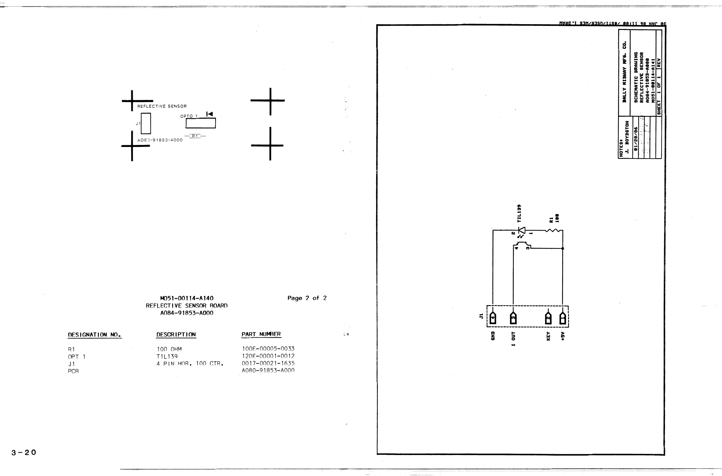
This page is a drawing, shown as the original scan.
C1 - C7
cP1 cp2
R1,R3, R2,R4,
ul U2
VRI = vR4
ua J2
PCMH1 = PCMH4
PCR DESIGNATION NO.
R6,RA,RIO R5,R7,R9,R11,R1 »RI2 yRI4 moO) 1986 BALLY MIDWAY MFG. CO LL RIGHTS RESERVED.
M051-00114-B142 REFLECTIVE SENSOR CONTROL BOARD A084-91854-R000
DESCRIPTION
1OOPF AX. CR.
-O1MF AX. CR. 1OMF AX. TANT.
100K OHM 10K OHM
ADCO0844 74HC244
50K POT.
13 PIN HDR. 100 CTR. 20 PIN HMR. 100 CTR.
SPACER #8 CONTROL PCB
0017- PART NUMBER
0639-00800-0003
0628-00800-0100 0986-00800-3400
100F-00005-0115 100£-00005-0088
0066-44 2BX-XXAX 0C75-00803-0001
9C75-00804-0001
0017-00021-1642 00021-1643
0017-00042-0320
A080-91854-R000 +5V
74HC244
ancess4 Slyrer vec {22
CHL cHe CHS CH4 2 AGND Ley Pale NOTES® J. BOYDSTON BALLY MIDWAY MFG. CO. SCHEMATIC DRAWING A084-91854-B000 MOS1-00114-B143
3-21
DESIGNATION LIST
DESIGNATION NO. DESCRIPTION
01,62 4.7 MF 25V RO TANT 3,04 22 MF 6V RD TANT c5,C6 470 MF 6V AX ELEC c7-c10 +1 MF SOV AX CER
cel 220 MF 25V AX ELEC CP2,cP3 +1 MF SOV AX CER
R1,R2 2.7K OHM 1/4 5% CRBN R3,R4 27 OHM 1/4W 5% CRBN RS=RB 1 OHM 1/20 5% CRBN
ut,U2 MB37 50
a 7 PIN Je 5 PIN
HSAT,2 HEATSINK ASSY
MH IMG 1/4" SPACER
UNLESS OTHERWISE SPEC. CONCENTRICITY T.1LR. . 002 FRACTIONAL +164 DECIMAL + .005 HOLE DIA. ANGLE ... + 12° DO NOT SCALE DWG. MCR/2 DUAL POWER AMP. Pc. A082-90910-Fo00
PROJECT ENG |C.MEDNICK Useyon TRON DIM. TOLERANCES CROSS REFERENCE LIST
| DESCRIPTION | ary | DESIGNATION NO. | PART NUMBER |
| «1 MF SOV AX CER | 6 | C7-C10, cP2, CP3 | 0986-00809-1190 |
| 4.7 MF 25V RD TANT | 2 | C1,C2 | 0986-00800- 3100 |
| 22 MF 6VY RD TANT | 2 | C3,C4 | 0986-008U0-1600 |
| 220 MF 25V AX ELEC | 1 | cP1 | 0986-00800-3200 |
| 470 MF 6V AX ELEC | 2 | c5,C6 | 0986-00809-1700 |
| 1 OHM 1/2W 5% | 4 | R5-RB | 0062-0260 3-1XXX |
| 27 OHM 1/4W 5% | 2 | R3,R4 | 9062-068B3~1XXx |
| 2.7K OHM 1/4W 5% | 2 | R1,R2 | 0062-19983-1XXX |
| B37 30 | é | U1,U2 | 11066-1 88XX-XX4X |
| TIN .045 SQ PINS | 12 | J1,J2 | 0017-00033-0439 |
| HEATSINK ASSY | 2 | HSA1,2 | A986-90010-E 000 |
| 1/4" SPACER | 4 | MH1-“H4 | 01 7-00042-0320 |
PC BOARD
DAN m7 SCALE
+ .002—.000 MECH CHK Cvilly THIS DWG 1S CONFIDENTIAL & PROPERTY OF BALLY/MIDWAY MFG CO [MIDWAY we FRANKLIN PARK, IL 60131
DUAL PWR AMP ASSEMBLY DRWNG A084 -90910-FO0O A080-909 10-F 090
REVISIONS PART NO. MO5 |-00986—FOIO
N.C. L. AUDIO
KEY V AUDIO
R. AUDIO ONoarnun — V AUDIO
DIM. TOLERANCES UNLESS OTHERWISE SPEC. CONCENTRICITY T.1.R. . 002 FRACTIONAL . £.1/64 Vv AUDIO
L. SHIELD
/2w RETURN
6V 23 cs c7 470 UF TUF R. SHIELD ‘ L.>— SHIELD
Vv AUDIO
R8 1 ! Vew \/2w
c10 i AUF
rR > SHIELD
V AUDIO a | + CPI Ts 220UF 25V F UF Vv AUDIO >> - PROJECT ENG: C.MEDNICK RETURN THIS DWG. IS CONFIDENTIAL 8 PROPERTY OF BALLY/MIDWAY MFG. CO. = = Cally (MIDWAY wee. co. . [ 6/14/84 se FRANKLIN PARK, It, 60131 DECIMAL ... .. *.005 HOLE DIA... +.002—.000 DUAL POWER AMP REVISIONS SCHEMATIC PART NO, ANGLE ...... 22° DO NOT SCALE DWG.
BRUNING:- 40-107 A080— 90910 FOOO MO5!1-00986-FOII
FOR ADDITIONAL ELECTRICAL INFORMATION, REFER TO MECH. DWG. NO. 0017-00003-0543. 3-24 — camaciron vawer Nn MicRoFABADS /VouTS. \, TESTOR VALUES ARE IN OUMS Yaw, S%, CF. NOTES: UNLESS OTMeRwise = SPEGIENED, CAMARILLO, CALIF. 93010 (005) 404-2851 eez 1 Al Ll J
| } | ‘tae! | | +izw Bia | ! |
qe) o% + 78
| tS aarz0os. | cos | + | MF |
ca >
| Pz | ‘ | mM. |
MF \2VAa arn 2 ™ ! ,™ \ 13h Ota I )HM ' OHI
| j | © | OK |
| © ' 5731
| ! | @) 45v @iza ~ | , |
| i | © | aa |
GI .
| i | @ | ATS |
| | | ©) | oe |
| | | © | ' |
| I : | Q | ' |
LO! com BO
| ! | @) | ® |
| | | 1 | nee2t |
©)
| - | a | I | * | ® | |
| | | 1 | coh oy | |||
| | | nine | PY 0° (ao 0} | a9 | ||
| 224 $ son | k | ' c. | ‘hw | os | |
| 470% | \/ico | cen | i | F | -BV@IA |
| coy | Ags | “ | e |
IN4934 @) cer ‘ = teB 10/50
| __ ILI | . | OPTOCOUPLER | cm | SZ |
+825] $7755 sm 2B 4 Low %, Bz re Ses : sm
| oe | f (0 i i | Loe % |
| ©) | ve | Seem ceenet |
moe Tas? 0-92. Rar n
| wPStTzt ae | wt | “ow | ~ sal |
0017-00003-0543 [ETE ie
DD NOT SCALE ORRAWING Schematic SP\O1o
sa Tce [owe mo, T= Dj 3\- SPIOIG Ix
This page reads as a drawing: its text was drawn rather than typeset, and comes out in fragments. See the original scan.
This page reads as a drawing: its text was drawn rather than typeset, and comes out in fragments. See the original scan.
BALLY/MIDWAY'S MAX RPM (2 PLYR) UR. #0075 ROM/EPROM PART NUMBERS
UNPROGRAMMED MONOBOARD A084~91787-C000 PROGRAMMED MONOBOARD A084~-91787~AC75
UNPROGRAMMED TURBO CHEAP SQUEAK A084-91779-B000 PROGRAMMED TURBO CHEAP SQUEAK A084-91779~AC75
M05 1-00C75-A008
2-28-86 RELEASE FOR PRODUCTION