Dominos TM-089 1st Printing Upright
Dominos (Atari, 1977) · Technical Manual · 60 pages · 16 sections · original scan
TM-089 1st printing
Operation Maintenance and Service Manual
WARRANTY
Seller warrants that its printed circuit boards and parts thereon are free from defects in material and workmanship under normal use and service for a period of ninety
- days from date of shipment. Seller warrants that its television monitors are free from defects in material and workmanship under normal use and service for a period of thirty (30) days from date of shipment. None of the Seller’s other products or parts thereof are warranted.
lf the products described in this manual fail to conform to this warranty, Sellers’ sole liability shall be, at its option, to repair, replace, or credit Buyer’s account for such products which are returned to Seller during said warranty period, provided:
- Seller is promptly notified in writing upon discovery by Buyer that said products are defective;
- Such products are returned prepaid to Sellers’ plant; and
- Seller's examination of said products discloses to Seller's satisfaction that such alleged defects existed and were not caused by accident, misuse, neglect, alteration, improper repair, installation or improper testing.
In no event shall Seller be liable for loss of profits, loss of use, incidental or consequential damages.
EXCEPT FOR ANY EXPRESS WARRANTY SET FORTH IN A WRITTEN CONTRACT BE- TWEEN SELLER AND BUYER WHICH CONTRACT SUPERSEDES THE TERMS OF THIS ORDER, THIS WARRANTY IS EXPRESSED IN LIEU OF ALL OTHER WARRANTIES EX- PRESSED OR IMPLIED, INCLUDING THE IMPLIED WARRANTIES OF MERCHANTA- BILITY AND FITNESS FOR A PARTICULAR PURPOSE, AND OF ALL OTHER OBLIGA- TIONS OR LIABILITIES ON THE SELLER’S PART, AND IT NEITHER ASSUMES NOR AUTHORIZES ANY OTHER PERSON TO ASSUME FOR THE SELLER ANY OTHER LIABILITIES IN CONNECTION WITH THE SALE OF PRODUCTS UNDER THIS OR- DER.
This document is and contains confidential trade secret information of Atari, Inc.
This document is loaned under confidential custody for the sole purpose of operation, maintenance or repair of Atari equipment and may not be used by or disclosed to any person for any other purpose whatever, and remains the property of Atari, Inc.
Neither it nor the information it contains may be reproduced, used, or disclosed to persons not having a need to know consistent with the purpose of the loan, without written consent of Atari, Inc.
DOMINOS
Operation, Maintenance and Service Manual
ATARI INC. 1265 BORREGAS AVENUE SUNNYVALE, CALIFORNIA 94086 408/745-2000 = TELEX 35-7488
By the Publications Group, Engineering Department AW
ATARI
Warner Communications Company fw)
All rights reserved. Copyright © 1977 by Atari, Inc. No part of this publication may be reproduced by any mechanical, photographic, or electronic process, or in the form of a phonographic recording, nor may it be stored in a retrieval system, transmitted, or otherwise copied for public or private use, without permission from the publisher.
For permission requests, write:
PUBLICATIONS GROUP ATARI INC. 1265 BORREGAS AVENUE SUNNYVALE, CA 94086
Lithographed in the U.S.A.
Subject INTRODUCTION 1.1 Physical Description of Game . 1.2 Summary of Game Play SPECIFICATIONS 2.1 General.... 2.2 Electrical... 2.3. Environmental .. 2.4 Owner/Operator Options for Structuring of Play . 2.5 Accessories Available on Separate Order . DESCRIPTION OF OPERATION .... 3.1 Functional Description of Game . 3.2 General Information ......... 3.2.1 3.2.2 3.2.3 3.3 Game Sequence 3.3.7 3.3.2 3.3.3 3.3.4 3.3.5 THEORY OF OPERATION .. 4.1 General Comments ...... 4.2 Components of the Microcomputer System TABLE OF CONTENTS
Page
Energizing the Game . TV Monitor ......+- TV Monitor Picture .
Operating Modes .. Attract Mode Ready-to-Play Mode Play Mode Operator Options .. DOVHHHnHubus VoBwWwYY BA
4.2.1 Program Memory ... 11 4.2.2 Read/Write Memory cai 4.2.3 Microprocessing Unii -13 4.2.4 Tri-State Devices . 13 4.3 The Microcomputer System .. +13 4.3.7 4.3.2 4.3.3 4.3.4 4,4 Microcomputer Watchdog .. 4.5 Components of Dominos Game Circuitry . 4.5.1 4.5.2 4.5.3 4.5.4 4.5.5 4.5.6 4.5.7 4.6 Self-Test Feature Program Memory Enable . RAM Enable Generation of Phase 1 and Phase 2 Signals ... RAM Output .......
System Clock and Sync Generator Playfield Generator . Video Output .. Manual Control Interface Tone Generator .... Topple Generator .. Audio Output. .
TABLE OF CONTENTS
Vi.
vil.
Vill. INSTALLATION INSTRUCTIONS ....................0.0 eee eee 19 5.1 Unpacking and Set-up Instructions . 5.1.1 Examination for Shipping Damage . 5.1.2 Mechanical Inspection 5.1.3 Setup of Light Box 5.2 Verifying Operation of Interlock Switch . 5.3 Operation of Game in Test Mode ..... 5.3.1 Putting the Game in Test Mode . 5.3.2. Game Responses in Test Mode .... MAINTENANCE AND ADJUSTMENTS ... 6.1 Routine Maintenance ....... 6.2 Adjustments of TV Monitor .. DISASSEMBLY AND ASSEMBLY ... 7.1. General Information ............ 7.2 Removing and Installing the Dominos PCB 7.3 Removing and Installing the TV Monitor . 7.4 Replacing the Fluorescent Tube TROUBLESHOOTING AND REPAIR ... 8.1 General Procedure............++++ 8.1.1 Identifying the Trouble Area . 8.1.2 Locating the Trouble Cause .. 8.1.3 Correcting the Trouble Cause . 8.1.4 Verifying Correct Game Operation ... 82 Test Equipment 8.2.1 Basic Test Equipment .. 8.2.2 Optional Test Equipment .. 8.3 Specific Troubleshooting Information . 8.3.1 Coin Mechanism .. 8.3.2. TV Monitor SCHEMATICS, DRAWINGS, AND PARTS LISTS .................- 31
LIST OF ILLUSTRATIONS
Figure 3-1 Functional Block Diagram Figure 3-2 Typical Picture During Attract Mode Figure 3-3 Typical Picture During Ready-to-Play Mode Figure 3-4 Typical Picture During Play Mode Figure 3-5 Locations of Switch Assembly SW 1 and Potentiometer Adjustments Figure 4-1 Dominos PCB Block Diagram Figure 4-2. Phase 1 and Phase 2 Signa! Shaping Figure 4-3 RAM Write Enable Signal Shaping Figure 4-4 TV Monitor Playfield Display Figure 4-5 Playfield Generator Character Trace for the Letter “’C” Figure 6-1 Location of Adjustments on TV Chassis Figure 6-1 Exploded Diagram
LIST OF TABLES
Table 3-1 Switch Settings for Operator Options Table 4-1 Operation of Multiplexer M8 With Given Input Address Table 4-2. Addresses of Switch Positions for MPU Data Line D6 D7 Input Table 4-3 Approximate Base Voltage of Transistor Q1 for Given Address Table 5-1 Numbers for ROM Test
This page carries no recoverable text. It is a drawing or a photograph. See the original scan.
|. INTRODUCTION
1.1 PHYSICAL DESCRIPTION OF GAME Atari’s Dominos is a one or two-player video action game packaged in its own distinctively styled upright cabinet that rests directly on the floor. A 23-inch TV monitor is mounted in the top front of the cabinet, with the monitor viewing screen tilted back from vertical. (Drawing number A007620-01, in Section IX of this manual, provides external and sectional views of the game cabinet.) The TV monitor viewing screen is covered with a plexiglas panel.
Player-operated controls are mounted side-byside on a panel directly below the TV monitor viewing screen on the front of the game cabinet. The consist of two sets of four pushbutton switches, (with one set on the left side of the panel and the other on the right), and two START pushbuttons (near the center of the panel). Indications of the effects on game play that result from depressing a pushbutton are depicted in the panel graphics that surround the two sets of pushbuttons. The START pushbuttons contain LEDs that will backlight these switches at various times during game operation.
Two identical coin mechanisms are mounted on the lower front center of the cabinet, below the player control panel. Either coin mechanisms can initiate play. The cash box is located behind a locked access door to the coin mechanisms.
Two speakers are also mounted on the front of the cabinet, on each side of the coin mechanisms. Both speakers produce identical sounds during game play.
1.2 SUMMARY OF GAME PLAY The player's objective is to have earned a higher point score than his opponent has when the game sequence ends. Dominos appear on the TV screen during play, and a player receives one score point each time the opponent's dominos fall down. The scores for each player are shown separately near the top of the TV screen. In a 1-player game the game’s internal circuitry automatically controls the opponent. The play sequence consists of individual “heats’’, and one point is awarded at the end of each heat. The play sequence ends as soon as one of the players achieves the maximum score.
At the start of each heat two arrows, one black and one white, appear first on the TV screen. These arrows then begin to move immediately at a rate automatically controlled by the game's internal circuitry. The arrows move alternately, one step at a time. Each time an arrow moves a step to a new position, a solid rectangular object is left behind in the arrow’s previous position. This object represents a domino, standing on edge. A trail of white dominos is left behind the white arrow, and black dominos behind the black arrow.
Players can control the directions of their arrow movement by depressing their pushbuttons on the player control panel, one at a time. The four buttons provided for each player govern arrow direction as follows: move straight up, straight down, to the right, or to the left. Depending upon the position of the player’s arrow at the moment a specific pushbutton is depressed, the game’s response will be to change the direction of that player's arrow by either 90 degress (to the right or to the left) or 180 degrees. However, a 180-degree change of direction will cause that player’s dominos to all fall down, one at a time, because the game's internal control circuitry interprets this situation as a collision between an arrow and the domino most recently placed behind that arrow. Collision situations also occur when an arrow moves against the solid boundary around the outside edge of the TV screen, against any domino (either one of its own or one of the opponent's) or against the other arrow. A heat ends a few moments after the dominos losing the heat have all fallen down. All dominos than disappear from the screen just before a new heat begins.
The movement of the arrows speeds up as the heat progresses, and as more and more dominos appear on the screen. This serves to increase the player's challenge because he or she must react faster and because more objects are appearing on the TV screen. The speed reaches a maximum value, however, after a given number of dominos have appeared on the screen.
During play various sounds are produced by the speakers whenever a new domino appears on the screen, when a collision occurs, and as each of the dominos fall at the end of a heat. These sounds provide an additional dimension to the game's animation and increase player appeal for the game.
The game has two options which the operator can adjust for maximum player appeal at a specific game site. One option provides three choices of game cost for a play sequence, and the other option provides four choices for the maximum score per play sequence. Paragraph 3.3.6 in Section III of this manual gives more information about these options. The game also has a speaker volume adjustment, and an adjustment for raising or lowering the pitch (frequency) of the sounds produced. Figure 3-5 shows the locations of these adjustments.
Whenever players are not using the game (the attract mode), the game’s internal circuitry causes game heats to be run automatically, one after another, with both arrows moving under control on the internal circuitry.
Section III of this manual gives additional information about the game’s design and describes the play sequence and scoring in more detail.
Il. SPECIFICATIONS
2.1 GENERAL
Cabinet Dimensions: Height 60% inches, Width 25% inches, Depth 23% inches.
TV Monitor: Black and white, 23-inch screen, with composite video input.
Coin Mechanisms: Two identical mechanisms accept only quarters.
Cash Box: Removable; located behind locked access door to coin mechanisms.
Power Cord: Approximately 6 feet long, extending from rear of game cabinet and having grounded threeprong plug for conventional wall outlets.
Power ON/OFF Switch: Toggle switch concealed on rear of cabinet near the top; intended for operator use only.
SELF TEST Switch: Located at the inside front of game cabinet, to the immediate left of coin box.
One 24-inch fluorescent tube for cabinet lighting. One GE #47 lamp for coin mechanism lighting. Lighting:
2.2 ELECTRICAL
Uses conventional grounded wall outlet providing 100 volts AC, 60 Hz, single phase. Power Requirement:
All fuses accessible from rear access door of game cabinet; TV monitor has two 3AG 1-amp slow blow, 250 volt fuses and remainder of game is protected by two 3AG 3-amp quick blow, Fusing: 250 volt fuses, mounted beneath the cover on the Electronics Tray Assembly.
This is a safety interlock switch located inside the game cabinet rear access door. It will cause removal of AC power to the game when the access door is opened. Power Interrupt Switch:
2.3. ENVIRONMENTAL
Operating From 32° Fahrenheit to 120° and Storage Fahrenheit (ambient tempera- Temperature Range: ture)
Maximum of 80% without condensation. Relative Humidity:
2.4 OPERATOR OPTIONS FOR STRUCTURING OF GAME PLAY
Cost: 25¢ for two players 25¢ per player 50¢ per player
Maximum Score: 3 points 4 points 5 points 6 points
2.5 ACCESSORIES AVAILABLE ON SEPARATE ORDER
Video Probe: Order from Atari Computer Test Order from Atari, catalog no. Fixture: CTF-1. Universal Test Fixture Buffer Board
Dominos Adaptors: Diagnostic Test Board (order
both from Atari; specify for Dominos game).
This page carries no recoverable text. It is a drawing or a photograph. See the original scan.
Il. DESCRIPTION OF OPERATION
3.1 FUNCTIONAL DESCRIPTION OF GAME The block diagram in Figure 3-1 illustrates the major functional parts of the Dominos game. Note that the game printed circuit board (hereafter referred to as PCB) sends a composite video signal to the TV monitor and two separate audio signals to the speakers.
3.2. GENERAL INFORMATION General information about the game in the following subparagraphs provides a background for the Installation Instructions in Section V of this manual, and the description of Game Sequence in paragraph 3.3 of this section.
3.2.1 Energizing the Game: The game is energized by inserting the AC power plug into an active AC wall outlet and placing the Power ON/OFF Switch in its ON position. The wall outlet must provide the AC power called out in the Specifications, Section II of this manual. The Power ON/OFF Switch is a toggle switch mounted in a concealed position on the rear side of the game cabinet, near the top right corner (when viewed from the rear).
3.2.2. TV Monitor: The game’s TV monitor is a self-contained transistorized television monitor. Because the composite video signal sent to the monitor by the control circuitry differs in many respects from the signal derived from commercial TV broadcasts, the picture appearing on the screen is unlike that of a home TV set and the monitor does not produce any sound.
3.2.3 TV Monitor Picture: The game’s composite video signal is constructed to produce only three video levels (white, gray, and black), instead of the more or less continuous shades of gray seen on a home TV screen. The background of the picture is gray video level. The main portion of the screen consists of a playfield which is surrounded by a wide boundary line. The left half of the boundary line is in black video, and right half in white video. The players’ scores appear near the top of the screen, just above the boundary. The score for the white arrow appears as a white numeral, and that for the black arrow as a black numeral. At various times during game operation, certain message lines appear on the screen. Some characters are written in black and some in white, and certain lines may be blinking on and off.
3.3. GAME SEQUENCE
3.3.1 Operating Modes: During use the Dominos game can be described as operating in one of four modes: attract, ready-toplay, play or test mode. Just after being energized the game starts out in the attract mode. It remains in attract until players deposit coins and these coins clear the coin mechanism, after which time the game changes over to ready-to-play mode. But it does not change over to the play mode until after the players have depressed the lighted START pushbuttons. The game remains in the play mode for as many heats as it takes for one of the players to earn the maximum score. After the last of these heats has ended, the game changes over to the ready-to-play mode if one or more game Credits are remaining, or else changes over to the attract mode if no game credits are remaining. The speakers do not produce sounds during the attract or ready-to-play modes.
The game's circuitry only recognizes the deposit of coins during the attract and ready-to-kplay modes. Therefore players should not deposit coins during the play mode, because the game will accept them but will neither give game credits nor return the coins.
The game is operated in the test mode for maintenance and troubleshooting purposes only. For a description of this mode and instructions for putting the game into this mode, refer to paragraph 5.3 in Section V of this manual.
3.3.2 Attract Mode: Figure 3-2 shows a typical picture that would appear on the TV screen at the completion of a play sequence in the play mode. The topmost line of words inside the playfield boundary tells the choice of game cost that has been selected in the operator
sovsce —|
wate anRow
mecca
seurresr Seruecnon a
Lis} wy tyme
eeu
composite
ign speaKen
Figure 3-1 Functional Block Diagram of Dominos Game
0 <> SCORECD> 6
1 COIN PER PLAYER
6 POINTS TO WIN GAME
Figure 3-2 Typical Picture During Attract Mode
option. The three choices for games cost will be displayed as follows: 1 COIN PER PLAYER 2 COINS PER PLAYER 1 COIN PER 2 PLAYERS The bottom line of words inside the playfield boundary tells the maximum score selected by that operator option. The four choices for maximum score are 3, 4, 5, or 6 points.
During the attract mode the game control circuitry will automatically move the arrows so that they appear to play game heats, one after another, continuously. However, no sounds are produced by the speakers and the score numerals do not change from what they had been when the previous play mode ended. Note that the topmost line on the TV screen, the words GAME OVER, will be blinking on and off.
3.3.3 Ready-to-Play Mode: Figure 3-3 shows a typical picture that would appear during the ready-to-play mode. A portion of the game’s internal circuitry functions as a game credit accumulator that can keep track of as many as 256 game credits. One game credit is subtracted from the accumulator at the beginning of a 1-player game sequence, and two credits are subtracted at the beginning of a 2-player game sequence. The only way that players can add credits into the game credit accumulator is by depositing money into the game. The number of coins required for one game credit is YOU HAVE CREDIT FOR 2 PLAYERS
a >
EACH PLAYERS PUSH YOUR START
Figure 3-3 Typical Picture During Ready-to-Play Mode
determined by the choice made in the operator game cost option.
After a play sequence ends, if no credit remains in the credit accumulator, the game changes over to the attract mode. Players must now deposit money in the game in order to add at least one credit into the credit accumulator.
As soon as the game has accepted enough money for one game credit, the game changes over from the attract to the ready-to-play mode. The picture on the TV screen changes as follows: the motion of the arrows freezes in the position that they had been at the moment that the game changed over to the ready-to-play mode. The top line of words inside the playfield boundary changes to one of the two following messages: YOU HAVE CREDIT FOR ONE PLAYER or YOU HAVE CREDIT FOR TWO PLAYERS. Also, the bottom line of words changes to the following: EACH PLAYER PUSH YOUR START which will be blinking on and off. The score numerals, however, will remain the same as they were before the game changed over to the ready-toplay mode.
Besides the changes in the picture just described, during the ready-to-play mode the LEDs inside the start pushbuttons will begin to blink on and off. Both LEDs will be blinking, even if only one game credit is remaining.
The game remains in the ready-to-play mode until the players depress the lighted START pushbuttons. If only one credit is remaining, as soon as either pushbutton is depressed, the game will change over to the play mode and both LEDs will go dark. Whichever START switch that has been depressed will determine the set of player controls to be used. The other arrow will be controlied automatically by the game's internal circuitry. If two or more credits are remaining in the credit accumulator, as soon as the first pushbutton is depressed, it will go dark, the second pushbutton will continue to blink on and off.
If the player wishes a 1-player game, then by merely waiting approximately 5 seconds, the game will automatically change over to the play mode, the other pushbutton will go dark, and a 1-player game sequence will begin. If two or more credits are remaining and players wish to have a 2-player game, then the second START pushbutton must be depressed within five seconds after the first START pushbutton has been depressed. The game changes over to the play mode as soon as the second lighted pushbutton goes dark. Both arrows will then be under player control.
Hf one or more game credits are still remaining in the credit accumulator after the last heat in the play mode has ended, then the game changes over to the ready-to-play mode instead. In this situation, the dominos are removed from the picture and only the two arrows remain.
3.3.4 Play Mode: Figure 3-4 shows a typical picture that would appear a few moments after a heat begins in the play mode.
2 SCORE 3
Figure 3-4 Typical Picture During Play Mode At the beginning of this mode, the score numerals are both reset to zero, all written messages are removed from the picture, and the two arrows begin to move. The black arrow always takes the first step, then the white arrow takes a step and so forth. After an arrow has moved to a new position, a domino is left behind in the old position, so that as time elapses, a trail of dominos is left behind each arrow. Both speakers produce a sound each time either arrow takes a step. The pitch of the sound is different for each arrow, so that the two sounds add to the players’ sensation of game animation. This first heat continues until one of the arrows strikes an object.
As time elapses during the heat, the speed at which the arrows take steps gradually increases until it reaches a maximum value. Of course, the step sounds also are made more frequently, increasing the players’ sensation of increased speed. The arrow blinks for a few moments when it hits an object, and the speakers produce a collision sound. Then the dominos behind that arrow topple over realistically, and the speakers produce a topple sound for each domino. The opponent receives one score point, and the heat ends after the last domino has toppled. The dominos are removed from the screen and only the two arrows remain for the start of the next heat, which begins immediately.
During a heat the player operates the four pushbuttons to alter the direction of his or her arrow's motion. The face of the control panel is labeled with arrows alongside each pushbutton to show players the type of response associated with depressing the pushbutton.
The play mode continues unti! one of the players earns the maximum score set up by the operator option. After the completion of the last heat in the play sequence, the game changes over to either the attract or ready-to-play mode, depending upon whether or not credits are remaining in the game's credit accumulator.
3.3.5 Operator Options: The game’s options (three choices of game cost and four choices for maximum score) are selected by setting the positions of four 2-position switches mounted on a game printed circuit board. The positions of these switches can be changed at any time at the game site.
To determine at any time how the switches have been set, simply note the game cost and POINTS TO WIN messages that appear on the TV screen during
Table 3-1 Switch Settings for Operator Options
Toggle Positions on Message on TV Screen Switch Assembly SW1 Option During Attract Mode 1] 27 37 4 J5,6, 7,8 | Description of Structuring _|
| Game | 1 COIN PER 2 PLAYERS | off| off] Always | Two game credits given for |
Cost on deposit of one coin.
| 2 COINS PER PLAYER | on | off | One game credit given for |
deposit of two coins.
| 1 COIN PER PLAYER | off} on | One game credit give for |
deposit of one coin.
| 2 COINS PER PLAYER | on}on | One game credit given for |
deposit of two coins.
Maximum] 6 POINTS TO WIN GAME | off| off Maximum score per play sequence is 6 points. 4 POINTS TO WIN GAME | on] off Maximum score per play sequence is 4 points. \5 POINTS TO WIN GAME | off] on Maximum score per play sequence is 5 points. 3 POINTS TO WIN GAME | on] on. Maximum score per play sequence is 3 points.
the attract mode. Table 3-1 shows these messages assembly, as described in Section VII, Disassembly and the corresponding switch settings for each mes- and Assembly, of this manual. Figure 3-5 shows the sage. In order to change the positions of the approximate location of the game structuring switch switches in the switch assembly, the printed circuit assembly, SW-1. board must be removed from the RF shield box
NOTES: For normal operation always leave SW2 in the “off” positions. Drawing not to scale.
—> increase
TONE 5 SPEAKER FREQUENCY 3 VOLUME Ss
Figure 3-5 Locations of Switch Assembly SW1 and Potentiometer Adjustments
This page carries no recoverable text. It is a drawing or a photograph. See the original scan.
IV. THEORY OF OPERATION
4.1 GENERAL COMMENTS This subsection provides a technical description of the Dominos electronic circuitry. Section IX of this manual contains schematic diagrams, assembly drawings, and parts lists referred to in the following subparagraphs of this section.
On the Dominos PCB schematic diagram, drawing number 007305, the symbol P (appearing at various inputs of the integrated circuits) indicates a connection to +5 VDC through one of the pull-up resisters R1, R2, R4, R33, or R38.
For easy reference, the Dominos PCB is divided into grid sections. These sections are identified by letters A through R (skipping letters G, 1, O, and Q because they may be easily confused with numbers 6, 1, and 0 respectively) for the short side of the PCB, and numbers 1 through 9 for the long side of the PCB. For example, sheet 1 of drawing number 007305 illustrates a NAND buffer R9 at the upper left-hand corner of the drawing. The component hardware of NAND buffer R9 will be found at coordinates R and 9 on the PCB.
The following circuitry discussion is separated into two sections; the microcomputer circuitry and the game circuitry. Figure 4-1 is a block diagram of the entire Dominos PCB.
4.2, COMPONENTS OF THE MICROCOM- PUTER SYSTEM
The microcomputer system carries out complex tasks of the game by performing a large number of simple tasks. Control of the system is the primary function of the Microprocessing Unit. This Unit causes the system to perform the desired operations by addressing the Program Memory for an instruction, reading that instruction, and then executing the simple task dictated by that instruction. Temporary storage of data necessary for the execution of future instructions, such as arithmetic operations, is stored into a Read/Write Memory. 4.2.1 Program Memory (Bottom Half of Schematic Sheet 2): Program Memory consists of read-only memories (ROMs), permanently programmed by Atari to execute the Dominos game. This memory has the capability of producing 8 bits of data for each of 4096 combinations of ones and zeros on the 13 address inputs. In computer terminology, this is stated as a memory size of 4k x 8.
The Dominos PCB is designed so that for the Program Memory two types of ROM devices can be used, mask-programmed ROMs or electrically-programmed ROMs (designated PROMs). The mask-programmed devices are programmed during manufacture of the device itself, and they have a memory capacity that is double that of the PROMs. The PROMs are electrically-programmed after their manufacture, but prior to being installed on the PCB.
At the factory all PROMs, all ROMs, or a combination of these device types may be installed for the Program Memory ona Dominos PCB. A table on PCB schematic sheet 1 shows the possible versions of the PCB, and lists device locations and device part numbers.
Since the data in the Program Memory is a permanent physical configuration of the ROM chips, the data is not lost when power is disconnected from the game or when the chip is removed from its socket. Since the Program consists of read-only memory, the result of an address input can only be the “‘reading” of data stored in the manufacturing process. It is not possible to “write” in more data.
4.2.2 Read/Write Memory (Top Half of Schematic Sheet 2): Read/Write Memory (RAM) consists of randomaccess memory, which actually contains eight random-access memories (2102-1s). Data may be stored in the RAM (called ‘‘writing” the RAM), then later recalled (called “reading” the RAM). Memory size of the Read/Write Memory is 1k x 8.
In order to read from the RAM, the R/W (pins 3) input of all random-access memories must be high to write into the RAM, R/W must be low.
Figure 4-1 Dominos PCB Block Diagram tow MONITOR
READ WaITE tone maewony . em GENERATOR
(ono 087) AUDIO AMLiER Yo SPEAKERS.
enocRan saemony ROM
ADDRESS artmact
smanuac "ADDRESS CONTROL DATA Inrenrace ——
As previously mentioned, data stored in the RAM is for the purpose of performing operations on data as instructed by the Program Memory. Since the RAM is a temporary storage area, removing power from the RAM chips will “erase’’ all stored data.
4.2.3. Microprocessing Unit (Left Side of Schematic Sheet 3): As mentioned earlier, the controller of the microcomputer is the microprocessor (MPU). From the MPU, a sixteen-bit address bus addresses Program Memory, RAM, and an Address Decoder. An eight-bit bidirectional data bus serves as a path for transferring data from Program Memory and to and from the RAM and other interfacing devices.
4.2.4 Tri-State Devices: Tri-state devices, such as E5 on schematic sheet 2, are capable of having normal logic output of ones and zeros when disable (pin 1) is low. When disable is high, the output becomes a high impedance. In other words, when disable is high, it is equivalent to completely removing device E5 from the circuit. ROMs and RAMs are also tri-state devices. Each ROM or RAM must be enabled by a certain logic level at its chip-enable input before the device is capable of outputting or inputting data.
4.3. THE MICROCOMPUTER SYSTEM The primary function of the Dominos Microcomputer is to instruct the game circuitry for the proper TV monitor display and audio outputs for corresponding manual inputs.
4.3.1 Program Memory Enable (Schematic Sheet 3): With initial power applied to the Dominos PCB, the MPU addresses Program Memory for an instruction by placing a 16-bit code at outputs ABO through AB15. The address decoder, consisting of ROM E2, one-of-ten decoders D2, F2, and £8, and addressable latch H8, receives the five most significant bits of this address code (address 9 through 13) as an instruction of which part of Program Memory to access. Outputs of one-of-ten decoder F2 enable only the individual ROMs of Program Memory required for the desired instruction.
4.3.2, RAM Enable (Schematic Sheets 2 and 3): Now, with the Address Decoder addressed for the enabling of the desired Program Memory ROMs, and Program Memory addressed for a data instruction, the MPU receives an 8-bit data instruction from Program Memory on the data bus. If this data instruction includes the storage of information, the MPU addresses the RAM and writes the data into the memory RAMs.
The procedure of writing into RAM is enabled by two signals; chip enable CE (pins 13) and R/W (read/write-pins 3) of the RAM must be low. The Address Decoder ROM (E2) receives an address (A9 through A13) and one-of-ten decoder D2 receives a high write signal from the MPU. The results of these signals is a low DISPLAY at the input of multiplexer K2 fora low chip enable CE at pins 13 of the RAM. The MPU also causes the R/W (pins 3) input to the RAM to be pulsed, via the WRITE signal. When this input is pulled low, MPU data on the data input to the RAM (pins 11) is stored into the RAM location determined by address inputs AO through A9.
4.3.3 Generation of Phase 1 and Phase 2 Signals (Schematic Sheet 3): Phase 1 (1) and phase 2 (62) are outputs of the MPU. Aphase 0 (60) signal is formed by shaping of horizontal synchronization pulse 4H by D-type flip-flop A7. The 4H input of A7 (pin 13) is fed twice through the flip-flop at a clock rate of 12.096 MHz. The output of the first flip-flop and the output of the second flip-flop are fed through an OR gate to produce the phase 0 (0) signal, as illustrated in figure 4-2. The MPU provides an output of 2 that is exactly like 0, except with a slight delay, and an output ®1 that is of an opposite phase of ©2. Signal 2 is fed through AND gate N3, which acts as a buffer.
When 1 is positive, the address and data lines of the MPU change and stabilize for the next output. When ®@2 is positive, the MPU addresses memory on the address bus and inputs or outputs data on the data bus. In order to guarantee that the MPU data is written to external devices at the proper time, write enable (WRITE, A7 pin 10) is shaped by NAND gate A8 and D-type flip-flop A7 as illustrated in figure 4-3.
Phase 2 is also used to control the output of RAM Address Multiplexer K2, J2, and H2. The multiplexer acts as a 12-pole double throw switch, switched at a rate of ©2. Again, as previously mentioned, the RAM is addressed by the MPU and data written into it when 2 is high. When ®2 is low, the RAM is addressed by horizontal and vertical synchronization and data is read out of the RAM.
4.3.4 RAM Output (Schematic Sheet 2): The RAM has a second data output latch that places the RAM data at the output of D-type flip-flop F5 and LS with the next rising edge of ®2 (clock input of F5 and L5).
4H
J8 pin 10
J8 pind
C3 pin 37
C3 pin 39
C3 pin 3
Figure 4-2 Phase 1 and Phase 2 Signal Shaping
4.4 MICROCOMPUTER WATCH DOG (Top Left Corner of Schematic Sheet 3): Watch dog is an external monitoring system that resets the Program Execution back to its initial instructions, if the program execution memory deviates from its intended sequence. This is acccomplished by a watch dog statement (address code) incorporated in Program Memory, that results in a TIMER RESET pulse at the output of the Address Decoder. This reset pulse must occur before decade counter C6 & 7 reaches the count of eight. Therefore if the Program Memory is functioning properly, a TIMER RESET pulse occurs within every eight frames of video. 4.5 COMPONENTS OF DOMINOS GAME CIRCUITRY The game circuitry receives game instructions from the microcomputer and responds with the proper video and audio outputs. Manual controls of the game circuitry provide control information as a data input to the microcomputer.
4.5.1 System Clock and Sync Generator (Top of Schematic Sheet 1): The crystal-controlled clock generates a 12,096 MHz clock frequency that is used to produce all of the operating frequencies of the game. Insert 1, supplied with the Sprint 2 manual, number TM-078, illus-
0 123 4°55 6 78 90 12 3 4 5 6
4H [Ld AB pin 2
2 | | A8 pin 5
Nac t ns ee A7 pin 10
330 1.120 NSEC NSEC I
Figure 4-3 RAM Write Enable Signal Shaping
: C
TO 1
HEH HHH
Figure 4-4 TV Monitor Playfield Display
trates the horizontal and vertical sync synchronization waveforms. Note that 9-bit binary counter (R8, P8, and N8) counts from 128 to 512, accomplished by tying bit 128H (pin 5 of N8) to a pull-up resistor. Also
The horizontal and vertical synchronization signals are used to produce a TV monitor raster made up of 262 horizontal lines at a horizontal frequency of 15,750 Hz (256H). Synchronized with line 224 is a vertical blanking pulse tht occurs for the duration of 38 more horizontal scans, resulting in the total number of 262 lines per frame. 4.5.2 Playfield Generator Left Bottom of Schematic Sheet 1): The Playfield Generator genertes both the playfield and all alphanumeric video for the TV monitor display. This is accomplished by the playfield ROM (consisting of ROMs P4 and R4 for a memory size of 512 x 8), shift register R3, and binary counter R2.
As illustrated in Figure 4-4, the TV monitor display is made up of thirty-two horizontal by twentyeight vertical grid sections. For each grid section, there is a byte of data (one byte equals eight bits DO through D7) in the microcomputer RAM. During the 2 cycle, the RAM is addressed by the MPU, at which time the desired byte of data is transferred from Pro-
gram Memory to the data input of the RAM. Then, during the 1 cycle, the horizontal and vertical synchronization signals can access each of these bytes of data as that particular grid is to be displayed. The RAM then outputs six bits of data (DISPLAY 0 through DISPLAY 5) that address any of the different alphanumerics and playfield characters stored in the Playfield ROM.
The Playfield ROM is programmed by Atari to provide eight bits of data for each of 512 addresses. The least significant addresses are from vertical synchronization 1V,2V, and 4V and the 504 most significant addresses are DISPLAY 0 through DISPLAY 5 from the microcomputer RAM. For each of the 512 addresses, there is one of sixty-four grid pictures, each being eight scan lines high.
The top of Figure 4-5 illustrates the letter “C’’ as it would be traced on the TV monitor display. The RAM would provide one six-bit address to the Playfield ROM for the letter, while vertical synchronization 1V, 2V, and 4V would complement the RAM address for each of the horizontal scan lines. The bottom of Figure 4-5 illustrates the output of shift register R3 for each horizontal scan.
Shift register R3 then loads the actual playfield or alphanumeric data from the playfield ROM and shifts it outin serial video (R3 pin 13).
Binary counter R2 latches data DISPLAY 7 from the microcomputer RAM. This results in the selection of white playfield video if DISPLAY 7 is high, or black playfield video if DISPLAY 7 is low. In actuality, only some alphanumerics, the left half of the playfield boundary, the black arrow and its dominos are represented in black video. The right half of the playfield boundary, the white arrow and its dominoes are represented in white video.
Binary counter R2 is also used to produce the COMP SYNC*, COMP BLANK", anid a 256H™* signal that are all delayed one character's width from their OH 1H 2H 3H 4H 5H 6H 7H
ov
Iv
2V
3V
av
5V
6V
7v
ov
3V
av LW
5V Le
wtJ LIL PL
Figure 4-5 Playfield Generator Character Trace for the Letter “C” 7V.
original timing. This delay is used to center the playfield onthe monitor's horizontal scan.
4.5.3 Video Output (Schematic Sheet 1): The Video Output circuit receives all video signals and gates them together through summing resistors R48, R49, and R50. The BLACK PLAYFIELD and WHITE PLAYFIELD signals are gated through a parallel path to produce a positive signal through resistor R50 and a negative signal through R49. The summed result is between a full ON condition (white) and a full OFF condition ( TV monitor display. hj, which is a grey jevei of the
Table 4-1 Operation of Multiplexer M8 with Given Input Address
Address Logic Level Output
| |ADR6 | ADR7 | 1Y (D7) | 2Y (D6)| |
| L | L | 1C0 | 2C0 |
| L | H | 1C1 | 2C1 |
4.5.4 Manual Control Interface (Left Side of Schematic Sheet 4): The main component of the Manual Control Interface is multiplexer M8. This component acts as a two-pole four position switch, operated by address lines ADR6 and ADR7 from the microcomputer MPU. Table 4-1 lists the input/output relationship of multiplexer M8 with the given Address inputs. Multiplexer M8 interfaces the information derived from the game’s various mechanically operated switches. These incluce: two coin switches, two sets of four pushbuttons for controlling directions of arrow movement, two START switches, the operator switches contained in miniature switch assembly SW1 (mounted in locations J8 and J9 on the PCB), and the Self Test Switch. All information is received by the microcomputer MPU when the MPU addresses the Address Decoderfor a low SWITCH signal that enables tri-state device K5 for a data output on the D6 and D7 data lines.
Coin information is a matter of storing in the microcomputer RAM the number of times a low logic level pulse appears on the data lines, when the appropriate address input of multiplexer M8 is being addressed. The microcomputer MPU only ‘looks’ for coin pulses during the attract mode and the readyto-play mode. Arrow direction information is “‘looked’’ for by the microcomputer MPU during the play mode.
Switch information is received by multiplexer M6 at inputs 1CO and 2CO. The microcomputer MPU addressed Decoders F9, H9, and J9 to determine if a switch is opened or closed. If closed, a low pulse will result for the given address as listed in Table 4-2.
5.5.5 Tone Generator (Top Right of Schematic Sheet 4): The key to the Tone Generator is the operation of transistor Q1 in conjunction with timer D7,8. Timer D7,8 operates as an oscillator with output frequency dependent upon the resistive charge path of capacitor C22.
Varying the collector-to-emitter resistive value of transistor Q1 varies the combined resistive charge path of capacitor C22 through transistor Q1 and resistors R21 and R23 in parallel with resistor R22. As the combined resistive value decreases, the output frequency of the timer increases. Variable resistor R23 makes it possible for the operator to manually adjust the frequency for a desirable tone at the game site.
The conductance of transistor Q1 is varied by grounding any combination of voltage divider resistors R5, R6, R7, and R8. The combinations of these resistors are determined by data from the microcomputer RAM, applied to the input of Latch D4. Table 4-3 lists the approximate voltages at the base of transistor Q1 for the sixteen different address inputs. These addresses cause a latch condition of Latch D4 only if a low FREQ signal enables Latch D4.
To derive a realistic tone, the output of Timer D7,8 is divided into separate frequencies by Divider Table 4-2 Addresses of Switch Positions for MPU Data Line D6 D7 Input
| o}/ | 1] | 2]3f4]5] | 6] | of | +] | 2) | 3] | 4] | 5) | 6} | of} | 1] | 2] | 3 | ||||
| ADRO | tL} | ui] | te} | aH} | ul | w]e | tc} | uw] | te] | wf} | ef | wry] | eu} | Hfetu | ||||
| ADR1 | cfu} | uf} | ar? | el} | ef | aw | foe} | ce} | wy | aw} | efef | ru] | eyeyuyiu | |||||
| ADR2 | t}oul | el] | uef | ul] | wf | ufe | c}ocfupyuyupu} | xf | xyxr | dx | ||||||||
| ADR3 | HH} | H] | Hi] | aH] | a] | aH] | WH] | WH] | WH] | HY] | HY] | HP | HP | a] | ep | eb] | eet | |
| ADRS | H} | H] | AH] | aA] | a] | aH] | Hw] | ef | ef | oe] | ef} | ef | eb | pe | |e] | HY | HW] | a |
| ADRS: | ete} | etut | ep | ute} | rt | utr} | ut | at | ulal | x} | x] | x} | x | |||||
| multiplexer | i | 2) |STARTSTART] SELF |HEAT] | $ | |||||||||||||||
| M6 input | 1 UP} 1 RT] 1 ON} LEFT | 2UP| 2RT}2DN| LEFT] | 1 | 2 | {TEST | #1 |MODE |
ACO (D7), 1 multiplexer HEAT] MB input #0 |MoDg 2CO (D6) 0
D8. A divide-by-three signal at QB (pin 11) output of D8 is applied to the four AND Gates C5. The four outputs from Latch C4 are also applied to these AND gates, and the gate outputs are summed through the resistor network R24-R27 to produce the TONE signal.
4.5.6 Topple Generator (Right Bottom of Schematic Sheet 4): The “topple” contribution to the game sounds, heard when dominos are falling, is produced at pin 11 of AND Gate A6. The inputs applied to this gate are the 4V timing signal and the TUMBLE signal derived from the MPU. Specifically, TUMBLE is produced at pin 5 of Addressable Latch H8 (shown on schematic sheet 3), whose inputs come from the MPU's Address Bus.
4.5.7 Audio Output (Bottom Center of Schematic Sheet 4): The summed signals of the Tone Generator and the Topple Generator are applied to one leg of a 5k-ohm potentiometer. Varying the wiper position of the potentiometer varies the signal input of Audio Amplifier D9. The output of the Audio Amplifier is connected to the game's speakers in parallel. By manually adjusting this potentiometer, the operator can increase or decrease the speaker volume at the game site.
4.6 SELF-TEST FEAURE Operation of the game in the test mode, as described in Paragraph 5.3 of Section V of this manual, provides on-the-spot testing of approximately 70% of the game. Circuitry tested includes the microcomputer MPU, RAM, motion circuitry Program Memory, game switches, and pushbutton lightemitting diodes (LEDs). Table 4-3 Approximate Base Voltage of Transistor Q1 for Given Address
Address
glolsl|g Base Voltage of $/S/3/% Transistor QI ELS/S]5 <x|<|=!l< cefat[ni[u
| of | efulule | 5.00 VDC | |
| rPHf | ul | ule | 4.25 VDC |
| atulul | cle | 4.08 VDC | |
| 3})H} | Hl | ete | 3.95 VDC |
a}clulalde 3.77 VDC
| s/H] | tl | H]e | 3.65 VDC | ||
| 6 | L | H | H | L | 3.52 VDC |
| 7 | H| | H | H | L | 3.42 VDC |
| 8 | L | L | L | H | 3.22 VDC |
| 9}H| | tl] | tl] | H | 3.13 VDC | |
| io} | L} Ht | a | 3.03 VDC | |||
| Ww) | H] | HL} | aH | 2.95 VDC | |
| 1} | ob | L | H|H | 2.84 VDC | |
| 13! | H | L | H|H | 2.77 VDC | |
| a4) | ob | H| | H]H | 2.69 VDC | |
| 15) | H|H | H|H | 2.62 VDC |
By addressing the RAM, writing the RAM with all possible combinations of data, then reading the RAM, the self-test thoroughly tests the individual random-access memory chips and the MPU itself.
By performing a check sum of all the data bits of the Program Memory, the self-test detects any error of the Program Memory.
Operation of all game switches is checked by the self-test operator, by listening for an audio output as each switch is activated manually.
V. INSTALLATION INSTRUCTIONS
5.1 UNPACKING AND SETUP INSTRUCTIONS
5.1.1 Examination for Shipping Damage: Before shipment from the factory, components and sub-assemblies of each game are carefully checked for proper operation. However, during shipment some adjustments may have changed or parts may have been damaged. Upon initial removal of the game from the shipping container, first examine the exterior of the cabinet. Then open the rear access panel and also examine the interior. Any shipping damage such as a dented, cracked or broken cabinet, sub-assemblies broken loose, etc., should be reported immediately to the shipper and to Atari, Inc.
5.1.2 Mechanical Inspection: After determining that the game has been received in good condition, carefully inspect the interior parts and verify the following:
- All plug-in connectors are firmly seated.
- The fuses are all seated in their holders
- No loose foreign objects are present (especially metal objects which could cause electrical short circuits)
- No harness wires have become disconnected or pulled loose. Be sure all major assemblies have been checked: game PCB, the transformer and other components on the electronics tray assembly, the two coin mechanisms, the speakers, all player controls, the TV Monitor chassis, and the light box assembly. (For shipment the latter item is left detached from the game cabinet.)
Do not go on to the remaining paragraphs in this section until the above mechanical inspection has been thoroughly performed.
5.1.3 SET-UP OF LIGHT BOX: Before putting the game into operation at the game site, the light box should be attached to the game cabinet. First insert the light box’s connector and wire harness through the hole provided in the top of the game cabinet. Then set the light box down into its final position on top of the cabinet. Next unlock and open the access door on the rear side of the cabinet, and inside the cabinet find the two threaded bolts that protrude from the light box into the cabinet interior, On each bolt attach a washer and a wing nut, and then tighten them down. Finally, attach the connector from the light box to its mating connector that forms part of the game’s wire harness, and then close and lock the access door.
5.2 VERIFYING OPERATION OF INTER- LOCK SWITCH The interlock switch is located inside the rear access door and is there to prevent accidental shock of anyone who has reason to stick a hand inside the cabinet. The function of this switch is to remove all power that goes into the game when the rear door is open. This switch is mechanically aligned by Atari, but it is important that it be checked to insure the proper operation after shipping.
After the completion of subparagraph 5.1.2 plug the AC Power Cord into the appropriate AC Power Source, set the Power On/Off switch to its on position. Within approximately 30 seconds, there will be a raster display on the TV monitor.
Verity operation of the interlock switch as follows. Unlock and slowly open the rear access door. The switch is operating correctly if, by the time the edge of the door has moved about 2 to 3 inches away from the cabinet, the disply on the TV monitor goes dark. While opening the panel do not insert fingers inside the cabinet and do not allow foreign objects to fall inside. If the raster display continues to appear on the TV monitor even after the door has been opened, immediately close and lock the door and unplug the power cord from the wail outlet. Then refer to Section VIil of this manual to replace and/or adjust the interlock switch.
Do not go on to the remaining subparagraphs in this section until the operation of the interlock switches has been satisfactorily veritied.
5.3. OPERATION OF GAME IN TEST MODE
PUTTING THE GAME IN TEST MODE: This game feature can speed up troubleshooting steps by quickly isolating many types of component troubles. In the test mode three types of tests are made: RAM, ROM, and Switch test.
Before the game can be changed over to the test mode, it must first be operating in the attract mode. When in attract, proceed as follows. Unlock and fully open the coin mechanism access door. Then find the Test Switch; it is mounted near the door’s hinge, about in the middle of the door opening. Placing this switch in its on position will change the game over to the test mode.
To change game operation back to the other modes, place the Test Switch in its off position.
5.3.2 GAME RESPONSES IN TEST MODE: As soon as it is put into the test mode, the game responds as follows. Immediately the first two tests, for RAMs and ROMs, are performed automatically. Afterwards the game is ready for the Switch test. In this case a person must, one at a time, manually activate whichever game switches are to be checked for correct operation. The three types of tests are described in detail below.
{a) RAM Test: The TV monitor will flash aphanumerics on the viewing screen.
If there is a RAM failure, the TV monitor display will freeze, with the alpha or numeric displayed on the TV monitor. You now know that this alpha or numeric is associated with the particular data code that failed the RAM test. The game will not go on to the other tests if there is a RAM failure.
If the RAM test determines that all RAMs are OK, the alphanumerics will automatically disappear after approximately 5 seconds, and the ROM test will begin.
- ROM Test: The ROM test will have no visual effect on the viewing screen, if all ROMs’ test results are satisfactory. If a ROM is not operating properly, a number will appear in the center of the TV monitor viewing screen, and will remain displayed there for the remainder of the test mode. The presence of a number means that a check sum error has been detected. Table 5-1 lists numbers that can appear and identifies which devices may be bad.
- Switch Test: Perform the following steps. For each step, the individual response will be a sound from the game cabinet speakers. Absence of the sound is an indication that the associated switch circuitry is not functioning properly.
Table 5-1 Numbers for ROM Test
Number Showing | Devices That May Be Bad
ROMD1, or PROMM1 or MO 1 ROM E17, or PROMN1 or NO 2 ROME1, or PROM P1 or PO
The LEDs inside the START pushbuttons will remain lighted continuously throughout the Switch Test.
- Depress each of the player pushbuttons for controlling direction of the arrows, one at a time (total of 8 pushbuttons).
- Depress each START pushbutton (total of 2).
- On the coin mechanism trip the left coin acceptor, and then trip the right coin acceptor.
VI. MAINTENANCE AND ADJUSTMENTS
6.1 ROUTINE MAINTENANCE NOTE
Due to its solid-state electronic circuitry, this The TV monitor is accessible only from in- Atari game should require very little maintenance side the game cabinet and these adjustand only occasional adjustment. ments have to be done while the game is . . energized. Therefore only persons famil- Game cabinets and glass may be cleaned with iar with safety measures and repair proceany non-abrasive household cleaner. If desired, dures on electrical equipment should perspecial coin machine cleaners which leave no re- form them. sidue can be obtained from distributors.
The monitor's adjustments function like those 6.2. ADJUSTMENTS ON TV MONITOR of a conventional commercial television set, except The TV monitor need be adjusted only when that the volume adjustment has no effect. Instead the picture is distorted, or if the contrast or bright- the game produces its sound in a speaker separate ness seem out of adjustment. from the TV monitor. Figure 6-1 shows the location
FUSES CONT BRITE VERT ~=HORIZ VOL HOLD HOLD
Figure 6-1 Location of Adjustments on TV Chassis
2 LIGHT BOX ASS’Y
FLUORESCENT TUBE
3 T.V. SHELF ASSEMBLY
4 CONTROL PANEL ASS'Y
15 CARD BOARD BEZEL
13 PLEXIGLAS RETAINER
14 PLEX DISPLAY SHIELD
Numbers refer to “Item” number used in parts list A007260-01, Section IX
Figure 6-1A Exploded Diagram, Front View
of the adjustments on the rear of the chassis. When making the adjustments follow these general guidelines:
BRITE (Brightness)—Perform this adjustment before the contrast. Adjust so that the white lines covering the screen just barely disappear, when the brightness is turned up. CONT (Contrast)—Adjust so that the images are as bright as possible against the dark background without being blurred. HORIZ HOLD (Horizontal Hold)—Adjust if the picture is slightly off-center horizontally, if the images appear warped, or if the picture is broken up into a series of diagonal lines. Adjust for a stable, centered picture.
VERT HOLD (Vertical Hold)—This needs adjustment only if the picture appears to be rolling up or down the screen. Adjust for a stable, centered picture.
9 DOMINOS PC BOARD ASSEMBLY
Numbers refer to “Item” number used in parts list A0O7260-01, Section IX 3 T.V. SHELF ASSEMBLY
Figure 6-1A_ Exploded Diagram, Rear View
This page carries no recoverable text. It is a drawing or a photograph. See the original scan.
Vil. DISASSEMBLY AND ASSEMBLY
7.1. GENERAL INFORMATION The following procedures are supplemented by Exploded Diagram, figure 6-1A and B, and by parts list and drawing A007260-01 located in Section IX of this manual. All capitalized component terms refer directly to the parts list.
When working inside the rear access door, always check to make sure that the interlock switch is not in the defeat position or stuck in the on position.
7.2. REMOVING AND INSTALLING THE DOMINOS PCB
- Unlock and open rear access door.
- Locate R.F. Shield Box Assembly immediately inside the rear access door. It is an aluminum box with many small holes. On one end of the box is a printed circuit board with an edge connector coming from the edge of the board. This printed circuit board is the R.F. Shield Assembly (PCB).
- Remove five pan-head Phillips screws from each of the long sides (total of ten screws) of the R.F. Shield Assembly. Carefully lift the R.F. Shield Assembly upward while pulling the Dominos PC Board Assembly straight out of the R.F. Shield Box Assembly. To install the Dominos PC Board Assembly, follow preceding steps (a) through (d) in the reverse order. DO NOT FORCE OR BEND THE PRINTED CIRCUIT BOARDS. BEFORE INSTALLING INTO THE R.F. SHIELD BOX ASSEMBLY, ALWAYS IN- SPECT THE TWO PRINTED CIRCUIT BOARDS FOR PHYSICAL DAMAGE. S
fe)
7.3. REMOVING AND INSTALLING THE TV MONITOR
- Unlock and open rear access door.
- Unplug the 12-pin Molex connector from the chassis of the TV monitor. z
id
(e
(f)
(gs
=
(i) Use a Phillips-head screwdriver to loosen and remove two #8 flat-head wood screws from the top side of the wood TV Shelf Assembly.
Remove the Control Panel Assembly by loosening and removing the four wing nuts that fasten the panel to the cabinet. Move the control panel aside far enough so that the TV Shelf Assembly is free to slide out of the cabinet.
With a Y-inch hex wrench, remove the two Button-Head Socket-Cap Screws that hold the Plexiglas Retainer.
Remove the black Plexiglas Retainer, then the plexiglas Display Light Shield.
Carefully remove the Card Board Bezel.
) Slowly and carefully, slide the TV Shelf Assembly up and out of the game cabinet.
To reinstall the TV Shelf Assembly into the game cabinet, follow the preceding steps
- through (h) in the reverse order. Before installing the TV Shelf Assembly, make sure the aluminum foil around the front edge of the wooden base of the TV Shelf Assembly is not damaged. \f damaged, replace.
REPLACING FLUORESCENT TUBE (a)
(b)
(c)
(d)
(e) With a %-inch hex wrench, remove two 1-inch #10-32 Button Head Socket Cap Screws from the top front edge of the light box assembly.
Remove the black Plexiglas Retainer, then remove the Plexiglas Display Light Shield.
Remove fluorescent tube.
Replace Plexiglas Display Light Shield.
Attach plexiglas screen with plexiglas retainer and two button-head screws.
This page carries no recoverable text. It is a drawing or a photograph. See the original scan.
VII.
8.1 GENERAL PROCEDURE
This section describes troubleshooting procedures in detail sufficient for a person with moderate technical ability to understand. However, for those interested in gaining more information on video game technology, especially the electronics, we recommend reading the Video Game Operator’s Handbook, manual no. TM-043. This book is available from Atari, Inc., attn. Customer Service Dept., 2175 Martin Avenue, Santa Clara, CA 95050 for $5.00 each, or from your distributor.
8.1.1 Identifying the Trouble Area: The first troubleshooting step should be to note all observable trouble symptoms. Examples of symptoms are: depositing a coin produces no game response, no sound coming out of the speaker at any time, no picture on the TV screen. At the same time also note the game features that still work. A systematic way of checking game operation is to perform the functional check given in Section V of this manual. Carefully train your eye to pick up all clues; by doing this an experienced troubleshooter can often spot the cause of a trouble even before he opens the cabinet.
Keeping these observations in mind, use the understanding of game operation gained from Section Ill, Description of Operation and Section IX, Schematics. Next narrow down the suspected cause of the trouble to a specific area or areas of the game: coin mechanism, TV monitor, harness or front panel controls (switches, lamps, speakers), electronics tray, printed circuit board or power cord. Be careful not to overlook possible trouble areas that may seem too obvious: a power cord plug that has worked loose from the wall outlet and is no longer fully seated in the receptacle, power ON/OFF set to the OFF position, or a rear panel access door that is not fully closed (thus causing the interrupt switch to block the AC power path to the game).
TROUBLESHOOTING AND REPAIR
8.1.2 Locating the Trouble Cause: Once a problem has been narrowed down to one or more areas, the next step is to perform various tests and measurements to isolate a specific cause of the trouble. Remember that sometimes a very complicated problem, such as erratic game operation, can be traced to a simple cause—the printed circuit board not being properly seated in its edge connector. Start with the most suspect area and trace backwards from the point where the trouble is first observable, using a process of elimination to eventually locate the faulty component, connection, etc. For example, if no sound is audible during game play, first check for a signal at the speaker leads. If no signal is present there, go back to the printed circuit board. If there is still no signal, then systematically check back through the various components of the sound generation circuit.
Substitution of parts is a legitimate and easy way to isolate the cause. For instance, if the PCB is the suspected trouble area, remove it and substitute a know-to-be-good PCB. Then check for correct game operation. Similarly, to check the TV monitor, connect the game to a known-to-be-good monitor. The harness can often be checked by substitution also. Substitute both a known-to-be-good PCB and TV monitor. If the trouble still persists, the harness must be at fault.
The test equipment for use in troubleshooting is discussed in paragraph 8.2.
8.1.3 Correcting the Trouble Cause: In practice, the steps required to correct troubles can range from simple adjustments (correctly seating the PCB in its edge connector, changing the setting on a potentiometer, adjusting the picture controls on the TV monitor) to repair of loose connections and replacement of defective parts. Extreme care should be exercised when removing integrated circuit devices and discrete components. Use a 40-watt maximum soldering iron with a small tip designed especially for IC work. To remove an IC device, follow this procedure:
Clip all leads and lift the IC package out, leaving two rows of leads. Then remove
leads individually with a soldering iron and needie-nose pliers. Finally, evacuate the holes with a solder sucker. Afterwards clean the area thoroughly, using an approved PCB cleaning solution to remove any traces of flux and dirt. Alcohol will do in a pinch, if necessary.
The microprocessor, read-only memories, and random-access memories are removed by simply pulling them out of their sockets. When placing them into their sockets, make certain they are placed in the correct socket.
Insert the new IC device using an IC insertion tool, making sure that the reference notch is oriented correctly and that the device’s leads are not bent during insertion into the board. Afterwards, be sure to solder each lead on both sides of the PCB, using as little solder as possible. After soldering, clean the area thoroughly to remove the flux.
Observe the same removal and insertion procedures when replacing discrete components. Trim the leads as close as possible and be sure to orient diodes and capacitors correctly.
8.1.4 Verifying Correct Game Operation: After locating and correcting the cause of a trouble, re-energize the game and perform a final check by placing the game in the self-test function, then check for correct operation during game play. Doing this will verify that your troubleshooting was correct. If the game operation is still not correct, go back and double-check your work, Make sure that any replaced components were installed correctly. If this was done properly, then start the troubleshooting steps over again. Keep in mind that there may be more than one trouble at a time, and that correcting one trouble can sometimes bring previously undetectable troubles to light.
This verification is especially important when the original trouble had been intermittent, that is, was not happening all the time.
8.2 TEST EQUIPMENT Electronic troubleshooting of a video game essentially consists of checking for the presence of various signals and of examining their condition. A signal can be thought of as acting like a ‘’messenger”’ that carries instructions from one unit or circuit to another. Many different types of signals aié produced in a video gamc, and for this reason several unusual and perhaps unfamiliar types of test instruments are used during troubleshooting. Each instrument has its own set of advantages and disadvantages for examining a given type of signal, and both the depth of the intended troubleshooting capability and budget will determine what instruments wil! be needed. Some instruments are basic and essential, no matter what size of service facility, while other optional instruments are desirable because they make troubleshooting easier and quicker.
8.2.1 Basic Test Equipment:
- The Video Probe. This is a simple but invaluable instrument having two leads—a test-clip lead and a test-probe lead. During troubleshooting of video signals the test-clip lead is left connected to the game side of the video coupling capacitor. On the Dominos this point is the junction of summing resistors R48 through R50 on the PCB. When the test-probe lead is then connected to any video developmental signal, that signal will be coupled to the video signal going to the TV monitor and a video probe picture will appear on the TV screen. The shape and other characteristics of this picture will give information about the signal being probed. The video probe is suited for troubleshooting synchronization and image signals, but will not be useful for extremely fast signals (such as the clock) or for very slow analog or digital signals.
A video probe can be constructed in a few minutes from these common electrical components: a length of 20 AWG (American Wire Gauge) rubbercoated wire, a 4.7K-ohm, ¥s-watt carbon resistor, and two test leads. For the leads, use a single Mouser test clip (Mouser #131C301 or 302) attached to one end of the wire, and a test prod containing the resistor on the other.
To assemble the video probe, proceed as follows: Remove the cap from the test clip and strip 3/16 inch off each end of the wire. Solder one end to the post in the test clip, thread the other end through the hole in the cap, and snap on the cap. Next unscrew the plastic body of the test prod from the point and trim both leads of the resistor to a 3/16-inch length. Solder one resistor lead to the inside of the point. Thread the other end of the wire through the hole in the body and solder it to the other resistor lead; screw the body back onto the point.
- The Logic Probe. This is a test instrument designed for fast verification of digital 1C outputs. {t is small, convenient to carry, easy to read, and rela-
tively inexpensive. The logic probe derives its power from the system under test; it has two power leads, one for connection to ground and the other to +5 volts DC. When the logic probe's tip is held against a digital signal point, three colored lamps in the tip will indicate the signal’s condition or state, as follows:
© The red lamp lit indicates a high or logic level 1 (for TTL components, this is +2.4 to +5 volts) @ The white lamp lit indicates a low or logic level 0 (for TTL components, this is 0 to +0.8 volt) @ The blue lamp lit indicates that the signal is changing states ® No lamps lit indicate the grey region between 0 and 1 (for TTL this is between +0.8 and +2.4 volts)
A circuit shorted to ground will illuminate the white lamp and an open circuit will illuminate the red lamp.
The logic probe is readily available from electronic supply sources; a commercial model found satisfactory is the Kurz-Kasch model LP 520.
- The Logic Pulser. This test instrument is similar in size and shape to the logic probe, and it also derives its power from the system under test. When the logic pulser’s tip is held against a digital signal point, the source and sink capabilities of the pulser override any {C output and the point is driven to the opposite logic level. If the point that the logic pulser is held against is low, pressing the switch on the side of the pulser will introduce a high pulse. Conversely, pulsing a high line will pull that line low momentarily.
During troubleshooting the logic pulser allows stimulation of in-circuit ICs with a shaped digital pulse. For example, a certain feature of the game may not be working and you suspect that a circuit is not receiving the necessary signal. Use the pulser to imitate that signal: if the circuit begins working, you have proved that the signal was in fact missing and you can begin tracking it down, This technique is very similar to jumping coils in electromechanical games such as pinball machines.
In addition to the regular “pulse” button, there is another switch mounted on the logic pulser. When this switch is set in the “rep” mode, the instrument pulses the digital signal point at a 5-Hz rate or 5 times per second. This extremely low rate is slow enough to allow watching events initiated by the pulser. Counter outputs, for example, are more easily observed when the counter is pulsed or clocked at this rate.
The logic pulser is also readily available from electronic supply sources; a commercial model found satisfactory is the Kurz-Kasch model HL 583.
- Oscilloscope. The most versatile test instrument, and also the most expensive, is the oscilloscope. The high-speed TTL integrated circuits used in video games produce fast-rise-time signals. The oscilloscope should have a 50-MHz bandwidth, dual trace and dual time base capability. These latter features allow examination of both input and output signals simultaneously, so that precise timing relationships can be checked. The oscilloscope should also have provision for internal or external sync.
Of the newer, solid-state oscilloscopes, a satisfactory model is the Tektronix 465.
- VOM or Volt-Ohmmeter. This common measuring instrument is extremely useful in video game troubleshooting. It can be used to check line voltage, transformer secondary windings, continuity, resistance, power supply voltages, and to some extent used for measurements in the analog circuitry.
One commercial model found satisfactory is the Simpson 260.
8.2.2 Optional Test Equipment:
- The Logic Comparator. This test instrument's main benefit is that it can be used to check the functioning of an integrated circuit device while the device is still in place on the printed circuit board. The logic comparator performs the check by comparing the suspect ICs functioning with that of an identical-type reference |C mounted in the instrument itself. Suppose that the functioning of a type- 74195 device on the PCB is suspected to be defective. First insert a program card with a known-tobe-good 74195 into the logic comparator, and then clip the comparator test leads onto the leads of the suspect device. If there are any logic state differences between the reference IC and the suspect IC under test, then an LED on the logic comparator will light up to indicate which output is not functioning correctly. Once a defective !C has been located, it should be replaced.
Logic comparators are readily available from electronic supply sources.
- Atari Universal Test Fixture. \n situations where a large number of video games are being serviced, investment in the Universal Test Fixture will be justified. This item of test equipment forms a test station for troubleshooting printed circuit boards after they have been removed from the game cabinet. The Universal Test Fixture has a full set of controls for operating the game and also has its own TV monitor. The game’s PCB is plugged into an edge connector mounted on the side of the Fixture; with this arrangement the PCB is positioned in a convenient way for connecting probes and other test instruments.
A program card inserted into a receptacle in the top of Fixture takes the place of the game’s interconnect wires. The program card thus sets up the Fixture for each particular game; the game’s name is clearly printed on the program card itself.
With the Universal Test Fixture the method of troubleshooting via substitution of known-to-begood parts is made fast and convenient. For example, suppose that the TV picture in a game is completely broken up and you want to determine whether the game or monitor is causing the problem. Remove the PCB and plug it into the Fixture’s edge connector, and also insert the correct program card for that game. If the picture on the Fixture’s monitor is correct, then you know that the problem lies in the game's monitor.
8.3 SPECIFIC TROUBLESHOOTING INFORMATION The following subparagraphs give additional troubleshooting information about certain areas of the Flyball game.
8.3.1 Coin Mechanism: If a player inserts a coin and the game does not respond, first check the coin mechanism. If pressing the coin rejector button forces the rejector mechanism to return the coin, then examine the coin to make sure that it is genuine. If it is, then use a set of your own test coins (which should include both very new and very old, worn coins) to determine whether or not the player's coin is undersize or underweight. If your test coins are also returned, this indicates that servicing of the coin acceptor portion of the coin mechanism is called for. Generally the cause of this particular problem is an improperly adjusted magnet gate. Inside the coin mechanism a magnet is used to test the metallic composition of the coin. Highiy magnetic coins, such as those made of steel or iron, will be retained by the magnet and can be returned by actuating the wiper operating lever. Coins having comparatively high magnetic properties will be slowed down by the magnet, and will drop off the end of the rail short of the “accept” entrance and be returned. Coins having little or no magnetic properties, such as brass or zinc coins, will pass through the magnetic field so fast that they will overshoot the “accept” entrance and be returned.
A magnetic gate adjusted with too large a gap may pass both genuine and counterfeit coins. An adjustment with too small a gap can lead to rejection of some or even all coins. Over a period of time, the screw that adjusts the magnet gate has a tendency to work loose, resulting in a gradual narrowing of the gate. At first, only the thickest (i.e., newest) coins are rejected. As time passes, more and more coins are rejected until finally player complaints lead to the calling of the game repairman.
If pressing the coin rejector button does not cause the coin to be returned, and if the game still does not respond, then check the coin mechanism to see if the coin is jammed inside.
If you are certain that the coin is genuine, and that the coin passes through the coin mechanism and into the cash box, then the lack of game response is probably due to some kind of electrical trouble. Check for signals at the electrical contacts of the coin mechanism before moving on to the harness and other parts of the circuitry.
8.3.2. TV Monitor: The TV monitor is a self-contained unit housed in its own chassis. A trouble’s cause may be narrowed down to the monitor—either by the substitution method using a known-to-be-good monitor, or by verifying presence of AC power to the monitor power supply and presence of the correct composite video signal. The entire monitor can then be removed from the game cabinet. Doing this facilitates troubleshooting steps, because all monitor components will then be accessible.
A schematic diagram of the monitor circuitry is included in Section IX of this manual. After disconnecting and removing the monitor from the game, standard TV troubleshooting techniques are adequate for locating causes of trouble. Additional servicing information is available from the monitor manufacturer (Motorola).
IX. SCHEMATICS, DRAWINGS, AND PARTS LISTS
NUMBER TITLE
A007260-01 Parts List and Drawing Final Assembly A007296-01 Parts List and Drawing Light Box Assembly A007292-01 Parts List and Drawing Control Panel Assembly A007287-01 Parts List and Drawing Electronics Tray Assembly A007310-61 Schematic Harness A007305-01 Parts List, Drawing, and Schematic Dominos PC Board Assembly (none) Schematic, Motorola Model XM 501/701 TV Monitor
DOMINOS.
PARTS LIST SPECIFICATION Page lof 1
ta Drawn ATARI & (sii Mech, Eng, Innovative Kee Games| Proj, Eng. Elec. Eng. Rev.
| leisure | ong bu | Mfg. Eng. | A |
Description | |Apprv4 Rev. | Description
—<——=—4
| Item | ___ Part Number | Qty. | Description | |
| 1 | A007261-02 | 1 | Cabinet Assembly with Graphics |
| 2 | A007296-01 | 1 | Light Box Assembly |
| 3 | A007268-01 | 1 | T.V. Shelf Assembly |
| 4 | A007292-01 | 1 | Control Panel Assembly |
| 5 | A007287-01 | 1. | Electronics Tray Assembly |
| 6 | A007299-01 | 1. | Rear Door with Lock Assembly |
| 7 | A003637-11 | 1 | Coin Door Assembly |
| 8 | A005912-01 | 1 | R.F. Shield Box Assembly |
| 9 | A007305-01 | 1 | P.C. Bd Assy, Dominos |
| 10 | A007307-01 | A | R.F. Shield Assy (PCB) |
| 11 | A003887-XX | 1 | Shipping Container |
| 12 | 007310-01 | 1 | Harness Schematic |
| 13 | 007290-01 | 1 | Plexiglas Retainer |
| 14 | 007289-02 | 1 | Plex Display Shield,Smoked |
| 15 | 007280-01 | 1 | Cardboard Bezel, Black |
| 16 | 000869-01 | 2 | Speaker, Alum. Cover |
| 17 | 48-002 | 2 | Speaker, 4" Motorola |
| 18 | 005233-01 | 1 | Rear Door Seal |
| ig | 006319-01 | 1 | Copyright Decal |
| 20 | 006305-01 | 1 | Printed Poly Bag |
| 21 | TM-089 | 1 | Tech nical Manual |
| 22 | 75-5124B | 12 | Bolt, Carriage, #10-24 x 1.50 Lg. |
| 23 | 75-010S | 12 | Washer, Flat #10 |
| 24 | 75-040 | 12 | Washer, Split Lock, #10 |
| 25 | 75-911S | 6 | Hex Nut, #10-24 |
| 26 | 75-931S | 7 | Wing Nut, #10-24 |
| 27 | 73-77004 | 8 | Rivets, 3/16" 0.D. x .68 Lg (.250 - .500 Grip) |
| 28 | 72-6612 | 4 | Screws, SM Pan Hd Phil. #6 x 3/4" Lg. |
| 29 | 82-1824 | 6 | Wood Screw, #8 x 14" Lg. Flat Hd. Phil. |
| 30 | 72-6610 | 13 | Screws, SM Pan Hd Phil. #6 x 5/8" Lg. |
| 31 | 78-25001 | 1 | Screw Down Tie Wrap |
| 32 | A006449-01 | 1 | On-Off Switch Assy |
| 33 | A007193-02 | ae | Harness, Power Switch |
| 34 | 72-6608 | 12 | Screws, SM Pan Hd Phil. #6 x 4" Long |
| 35 | 72-6808 | 1 | Screw, SM Pan Hd Phil. #6 » %" Long |
| 36 | 007103-01 | 1 | On~Off Switch Cover |
| 37 | 78-6601216 | 1 | Alum. Foil, 1" Wide x (Approx 8" Long) |
2 ene SECTION =e
“EINAL ASSEMBLY,
DOMINOS
| aSc7260-01 [A a oc
(ues i
se t )
wires omttns)
A072 92- OF z Zz cal f a YL < po 7900.
TO “s $ @
SECURE To RE BOX IN FINAL AY
J og
] L, (22.
® Oz les Rean VT ax
| Bice | OF | i | 7 |
Reqo Vee Bic /W in SN i] w @ +—) WIP TEST SWITCH BR @) & SKETCH A exw REQD ee (
To e ON-OFF SW
| OR Y BUW W | YONI OY | 1 |
ono | am
| [ASSEMBLY TITLE | /AUscTONTCS War ASSEMBLY PJ Larose?) | TES | TT |
‘PARTS LIST SPECIFICATION Pagel of 2 7 Draws” wun ASS_ANOTZODCOT
| ATARI | Checked | Mech, Ege | | | 45666 | 16143 |
| Pal | ay | Te | a | ||
| Mig. Eng. | iB | Qe BK YE Gu! | GN” BN BN | ||
| Deseription | Date Parpre] Reve | Description | Date [Apert | PRIMARY | SECONDARY |
Pros 3 [rer fer Soo TTT
ten | bat Nonber [8-] Deseription
L ‘Tray, Eluctronies
Label former, C0135 Cover transformer
ame
/ Tatecloee
Plu, Pouer Lae, = awe
Phil we 8 us ten yeas 3/4 a PANEL , COUN DOOR, & SPEAKERS
3 aw MH SOLDER TO TEST SwiTCH Set SKETCH A
ATARI. INCORFORATED Neo onc (os'Guton
re 5330
DOMINOS ELECTRONICS TRAY ASSEMBLY
Narre
SCHEMATIC HARNESS: Anse ONTLBOHS,
a,
SRST ISEISS
This page carries no recoverable text. It is a drawing or a photograph. See the original scan.
=le]e
318/83) ans [et ifnolan fuolesfeot } [Assespiy HALE — PUL corravso: | [ASSEMRIY TLE pou Pil Tai CT SPECIFICATION ce Tans HRT SPECTATOR nes | Beam oe cH Dacron
| ed s L na 1 — : ™ ASSEMBLY,
- oe sn i DOMINO B.C. BD.
ID] Ao072065-1x a Ce Ce
This page carries no recoverable text. It is a drawing or a photograph. See the original scan.
This page reads as a drawing: its text was drawn rather than typeset, and comes out in fragments. See the original scan.
NOTES: UNLESS OTHERWISE SPECIFIED
- RESISTANCE VALUES AEE IN onMs. 2 CAPAC\TANCE VALUES ARE IM MICRO FARARDS. eR33
s_|o fo | 22 Ps GE NB chs Xo Dae >a
203 MR itd wy Pay
VOLANEK VeCANK x j—— YRESET
-- VBLANK
————vsne,
e
R2,4,33,38, ic
yov— - \ 46y ev ©,13-19,20,21,26, 27,29, 31 95,4193, 48,1015 omy @ [VIGED OUT
sw VIDED GND
AS —2[6S)*-* Bos wait PLAY rie SYNC PLAYFIELD AND POWER CREWIT 2 AS 7 S)24 See ER PAV ETS
ATARI
SCHEMATIC . BOMINOS
HGMALS 22 PIN NO. PIs, SEXCEPT WHERE
Dass
© PLACES. EXCEPT WHESE SHOWN
SS Rou
SPUN 2 pha ae
MEMORY
ATARL INCORPORATED
SCHEMATIC DOMINDS
TIMER, REDET (TEST) Logs a8.
yf ev aauee
alte .
ey i a3, a 7 : AO eset
rename
Bw ——4, Vr. Es §2—§ op 2lany an a i _— ere a
Write
an
Iw. VAC. D7 o3
20-6009
JK) UB2 OBS 6 CHS 6% Car 45/4 AGIA
ARIS
ARIZ AGI
ABIO ABO
ABS
AB7
Syne
ABG
ABs ft
ARe
ge
ca
136129 123
De
os
D3
D2-—.
ot
op —
+5
cel Ine
Rie ATTRACT
VRESET
VBLANK A Ris
piers eek
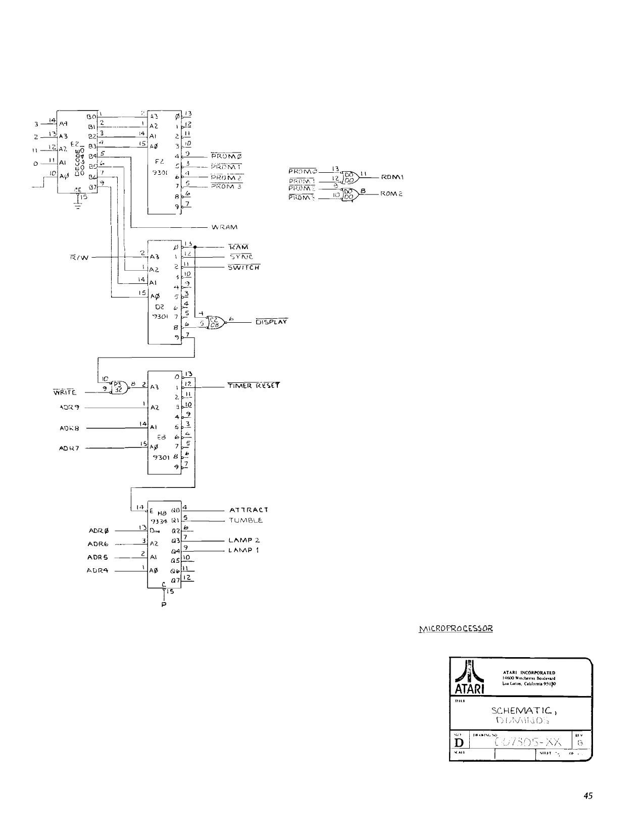
This page is a drawing, shown as the original scan.
This page reads as a drawing: its text was drawn rather than typeset, and comes out in fragments. See the original scan.
ju
P p—* DISPLAYS ——+ +4 ”
DISPLAY |
DISPLAY +
DISPLAY 3 + ATTRACT
z
FRea
Ree TOPPLE 33K Reo TONE tor D>: [5B — ree Jao Rar ROE Sh3p KPA DB
cra Sey 2 nav ac ep eM Ewe 220K Tew ys 18 e FRE Lass PPE ea, 2a? aro =
sv
| 5 | - | 10 |
tT css *
| valle | Aes | TONE, |
| 2h | wal! | 4. |
ca BE tie 7 lap aS: ary ale |
| ely | vat? | 268 |
3 m Or easN i
| ri | 2al'S | velee |
| eo | Sha | cw |
2a}
te0v
vou Abs flo | fa fis hey
| Reed CSF | be | H— 21] Aupio |
sedi} rox ioss — [| oso ay — 2 23v ted ALDIO TUMBLE 2} ond
RP
FREa
A ATARI [ATARI INCORPORATED Tae Winchester Boers Vernon, Calfrnia 95030
SCHEMATICS y DOMINOS
007305 -xx [6 |
a7
BWA Sa
Mung MIDWNOD 3003 25
This page carries no recoverable text. It is a drawing or a photograph. See the original scan.
This page carries no recoverable text. It is a drawing or a photograph. See the original scan.
This page carries no recoverable text. It is a drawing or a photograph. See the original scan.
ATART Innovative leisure
ATARI INC. 1265 BORREGAS AVENUE SUNNYVALE, CA 94086 408/745-2000 e TELEX 35-7488