Pepper II Operation and Service Manual 2nd Edition
Pepper II (version 8) (Exidy, 1982) · Manual · 73 pages · 25 sections · original scan
Pepper I
Operation and Service
Manual 2° Edition
PEPPER II™
Operation and Service Manual 2nd Edition
© 1982 Exidy, Inc. Exidy Ireland 390 Java Drive, Sunnyvale, CGortlandroe Industrial Estate California 94086-1271 Nenagh, County Tipperary Telephone: (408) 734-9410 Ireland Toll-free: (800) 538-8402 Telephone: (067) 32555 Telex: 357-499 (EXIDY MNTV) Telex: 70009 (EXDY El)
COPYRIGHT
Copyright © 1982 by Exidy Inc. All rights reserved. No part of this publication may be reproduced, transmitted, transcribed, stored in a retrieval system, or translated into any language in any form, or by any means without the prior written permission of Exidy, Inc. 390 Java Drive, Sunnyvale, California 94086.
DISCLAIMER
Exidy Inc. makes no representations or warranties with respect to the contents hereof and specifically disclaims any implied warranties of merchantibility or fitness for any particular purpose. Further, Exidy Inc. reserves the right to revise this publication from time to time in the content hereof without obligation of Exidy Inc. to notify any person of such revision or changes.
TRADEMARKS
PEPPER 11” is a trademark of Exidy Inc.
This equipment generates, uses and can radiate radio frequency energy and if not installed and used in accordance with the instruction manuals, may cause interference to radio communications. As temporarily permitted by regulation, it has not been tested for compliance with the limits for Class A computing devices pursuant to Subpart J of Part 15 of FCC Rules, which are designed to provide reasonable protection against such interference. Operation of this equipment in a residential area is likely to cause interference in which case the user at his own expense will be required to take whatever measures may be required to correct the interference.
EXIDY PEPPER II™ OPERATION AND SERVICE MANUAL
TABLE OF CONTENTS
PRELIMINARY PROCEDURES ...sccesccscevecevceccscer I
A.
Be
cory
De GAME INSPECTION .eeseeee
- Filing a Claim ..s...00e
- Visual Inspection crcccccccccescccccecsees 7 ee eeceeeee T eeeeeeree 1
INSTALLATION sececccccecccescecscecccceescees 2
PRELIMINARY CHECKOUT PROCEDURE .. eereerree 2
ADJUSTMENTS cocsesccccccccccccrecccccssesnces
- Power Supply Information and Adjustments .
- Audio Board Adjustments «sss.
- Operator Selectable Options wecceecscssece a. Coinage b. Number of Turns c. Bonus Turns a ewececeeeee 3
MODES OF OPERATION .cescesccoeecece 6
A. AUTOMATIC SELF-TEST MODE .... 6
- Logic Diagnostic Tests .. 6 a. The RAM Test. b. The ROM Test
- Audio Diagnostic Tests ...
- Control and Color Diangostic Tests...eeees 8 eee cree eeeneee 7
THE ATTRACT MODE cecececccccccssecccrcescecee 9
INTRODUCTION MODE .sceccecscccsccccccrsceeeee F
GAME PLAY MODE .eceeeees eee 10
- Obstacles and Hazards eee 10 Ze SCOTING cesececccecccerccccccssercessceee 10
VANITY MODE .eseeescccccsrcccseveccncseesece 10
APPENDIX A: SCHEMATICS
MEMORY MAP cooccccsccececcccscccssccvccssccees And
Page
Page
Page
Page
Page
Page
Page
Page 1: GAME LOGIC cececesccccecevevccsevesses An2
Master Oscillator, Element (Horizontal) Counters, Line (Vertical) Counters, Screen RAM Addresses, Coin Input Decoding, Hardware Generated Line Positioning Proms, Blanking and Video Clocking, Black and White Composite Video Output
2: LOQiC ceeveeccrccvevevecccccseeveecese Aq3 Screen Controller PROM, Screen RAM Character Image Storage, PROM Power and_ Signal Selection, Character Generator Output Shift Register
3: Plane Interface Board .seseseeceseeees An4 Character Generator Image Storage RAM
4: LOZIC cececccesececceccccsescsveseesees AWS The 6502 Microprocessor, Power-on Reset circuit, Processor Workspace RAM, Main Address Decoding
Bi LOZIC evecccceveacccevecsevesseeeeeses AMG Program Memory, PROM Address Selection, Memory Device "Personality" Selection
6: LOQIC seccecccvvcccccscevvcccccscesees An7Z Moving Object Horizontal Position, Moving Object Vertical Position Counters, “Write Moving Object" Decoding, Color Interface Qutput
7 LOBIC cecccccccvececesvccccvceccsceses AWB Moving Object Multiplexing, Moving Objects Image PROM, Moving Object Video Output Shift Registers, Moving Objects Shift Register Load Logic, Moving Object Shift Register Control Logic, Memory Device Personality Configuration
B Of B: LOGIC covesccccvecccvcccceeceseee AWD Interrupt Status Latch , Option Switch Port, Control Inputs Port, Moving Image Latch, Audio Board Port, Control Port Latch, 1/0 Decoding
AUDIO/COLOR PCB-GENERAL DESCRIPTION ..eeeeeees AH10
Page
Page
Page
Page
Page Logic and Power Interface, Communications and Address Decoding
6502 Microprocessor, Peripheral Interface Adapters, Address Decoding, Music Generator, Master Oscillator, Program Memory, Output Filter
Clock Manipulation and Noise Generation Circuit, Amplitude Modulation Control, Output Summation and Volume Control
Summing Amplifier, Integrator and Audio Power Amplifier
Pattern Character Color Division, Priority Encoder, Color Data Latches, Color Selection Multiplexers, Video and Sync Signal Polarity Selection, Final Video Output Re-sychronization
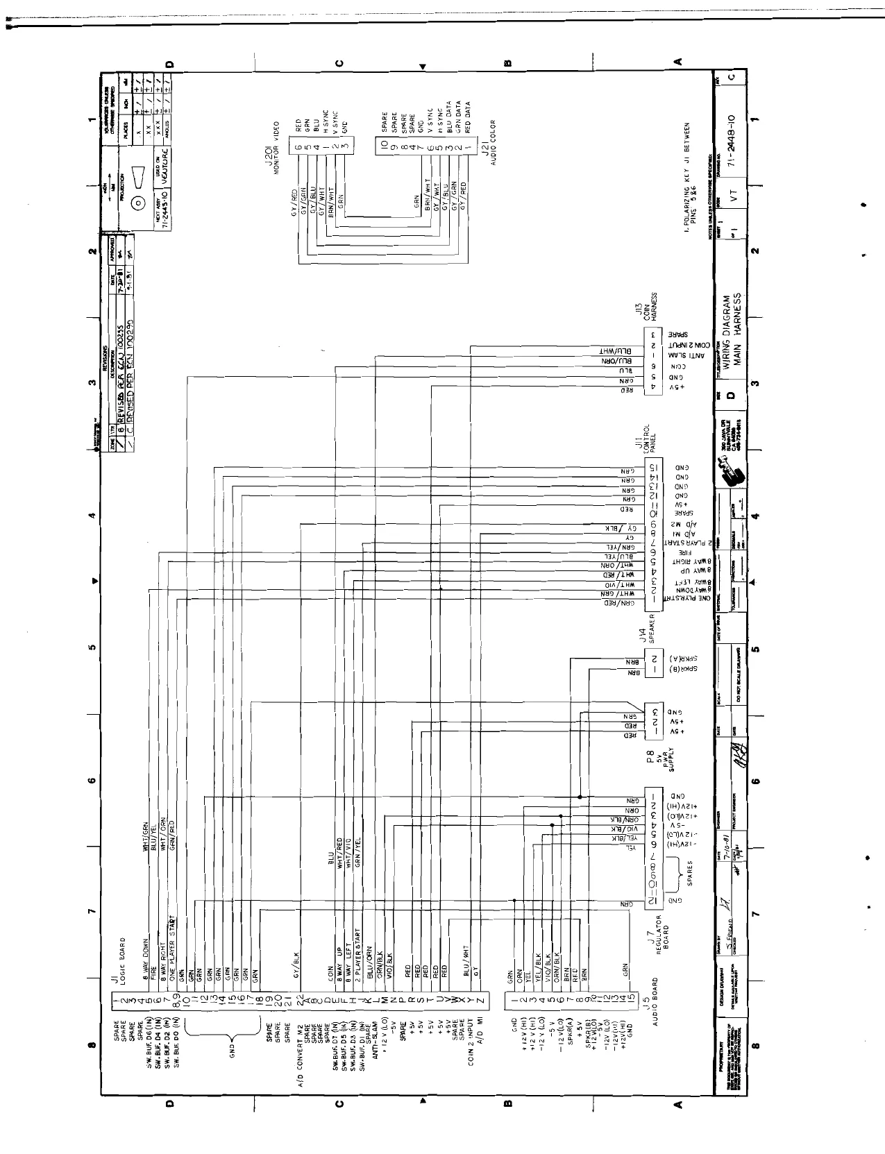
Wiring Harness Diagrams Main Harness, Control Panel Harness, Coin Door Harness, Electrical Schematic for Universal Power Supply
APPENDIX B: ILLUSTRATED PARTS LIST
Ae
B.
c.
dD.
Ee FINAL ASSEMBLY «ssssoee
CONTROL PANEL ASSEMBLY .ccscccvscecsccceccccece
JOYSTICK ceccececccccccecsssccceensseesssnceees
UNIVERSAL POWER SUPPLY .ecesesscccccceccerenees
ISOLATION TRANSFORMER ASSEMBLY seseccceseoccres
COIN DOOR ASSEMBLY sessscccecsssccccesccsosssee
LOGIC AND AUDIO BOARD ASSEMBLY ssssseeeesescens
PRINTED CIRCUIT, UNIVERSAL POWER SUPPLY «esesee 1: AUdiO/COlOrecevececssccesesseseceseecs AT
5B: AUdiO/COlOrseesecesceeececccssserecees AWTS 2: Audio/ColOr sesecccevecsccececcesesecs Ant2
3: AUGiO/COLOL sscccecesesececserececsees An13
4: Audio/Coloressccssccecessereccessecees An14
B-6
B-8
B-9
LOGIC BOARD .eccecccecccccccccrecccccseceeeves Br10
AUDIO/COLOR BOARD ASSEMBLY ceescevecceseeeeeee B-11
PLANE INTERFACE BOARD ...+. peace eeceeeseees B13
FOREWORD
Part One of this manual is on Preliminary Procedures, describing game inspection, installation, and checkout. Also, adjustment procedures are given for power supply, audio volume, and Selectable Options.
Part Two, Modes of Operation, describes the four PEPPER I!| modes: Automatic Self-Diagnostic Test Mode, Attract Mode, Game Play Mode, and Vanity Mode.
Appendix A contains game schematics, with a circuit description on the page opposite them.
Appendix B is the Illustrated Parts List. Parts are pointed out in the drawings and listed opposite each drawing. .
PRELIMINARY PROCEDURES
A. GAME INSPECTION
All Exidy equipment is carefully packaged in well-padded cardboard containers to prevent damage during shipment. Before signing the delivery receipt, you should follow this procedure:
1.
2.
3.
1. Check for obvious damage and make certain that the physical piece count of the shipment matches the piece count on the bill of lading. These two procedures should always be done before signing the delivery receipt.
Shortages and/or obvious damage to the packaging on any given shipment should be noted in writing on the delivery receipt before signing for the delivery.
If concealed damage is suspected on any shipment, those packages believed to contain the damaged goods should be opened in the presence of the delivery driver. If the goods have sustained concealed damage, a description of said damage should be noted in writing on the delivery receipt before signing for the delivery.
Never apply power to any game with noticeable damage.
Filing a Claim
To file a claim, follow this procedure:
1.
2.
3.
2.
2.
3. Any and all damaged freight, including packaging, should be retained by the consignee until a physical inspection of said freight can be made by a representative of the carrier involved.
The Claims Manager for the carrier involved should be notified as soon as possible, after the damaged goods are received. Preferably, the carrier's Claims Manager should be notified within forty-eight (48) hours of receipt of the goods by the consignee.
If warranted, a written claim should be filed with the carrier involved. A detailed description of the damage(s) should be provided and copies of all supporting documents, including bill of lading and/or delivery receipt, inspection report, and invoice, should be attached.
The sooner a claim is filed, the better for all parties concerned. The carrier against which a claim is filed is required, by law, to respond to (acknowledge) that claim within thirty (30) days of receiving same and must reach a final disposition in the matter within one hundred twenty (120) days.
Visual Inspection
Remove the rear access door with the appropriate packaged key.
Examine each major and electrical component thoroughly for scrapes, dents, broken or missing parts and loose or missing screws.
Check for loose cable connectors.
- - Visually verify that all the integrated circuit devices ({C's) plugged into sockets are properly seated and that no IC pins are bent or misaligned.
If you find any damage during this inspection, file a claim with the carrier. Send a complete report of the damage to Exidy Inc.
B. INSTALLATION
Planning the location of the game should involve both physical and electrical considerations. Such physical considerations concern the placement of the equipment with respect to these clearances:
Height: 72.50 inches, 184.2 cm. Width: 25.50 inches, 64.8 cm. Depth: 31.00 inches, 78.7 cm.
An indoor, relatively dust-free environment is necessary, with proper conditions required of any electrical component. Electrical considerations include availability of an AC outlet with the correct voltage and frequency. You should consider the working space required for technicians and operators incuding access to the rear of the game.
C. PRELIMINARY CHECKOUT PROCEDURE
After properly installing PEPPER {1™, we suggest following this procedure to check its operation:
- Plug the AC jack into the AC outlet.
2 Once powered up, after five seconds of silence, a quick beep sounding like an organ chord, is heard. This is part of the Exidy Audio Diagnostic Test. Asingle beep indicates all is well with the audio board. If more than one beep is heard, consult Part (1, Automatic Diagnostic Test Mode.
- Allow 8-10 seconds to pass for the CRT to warm up.
- Observe the TV monitor display to assure the correct attract mode is present on the screen, as described in Part 11 B, Attract Mode. If the PEPPER II” display is incorrect, contact Exidy Customer Service Department.
- Insert the appropriate coin or token into either of the coin slots. All the messages in the attract mode will flash the following line:
PRESS PLAYER ONE START or PRESS ONE OR TWO PLAYER START
depending on the number of coins dropped into the coin slot.
6 Press one or two player start and play the game to verify that all screen images are displayed as described in Part 11 D, Game Play Mode.
Screen colors may possibly be affected by the relative position of the game with respect to the earth's magnetic field. If this condition occurs on your game we suggest rotating the game to the RIGHT or LEFT. Also, by powering the game ON and OFF, the internal degaussing unit should eliminate any color deficiencies. In the event that this does not correct the monitor colors, externally degaussing the game will eliminate the affected colors.
If assistance or repairs are necessary, contact the Exidy Customer Service Depart ment, (800) 538-8402.
D. ADJUSTMENTS
- Power Supply Information and Adjustments
All DC Power required to operate PEPPER II” is supplied in the Exidy Power Supply Module. These supply outputs are as follows:
| +5v DC | @ | 6 amps | |
| -5v DC | . | 2 | 1 amp |
| +12v DC (HI) | @ | 3 amps | |
| +12v DC (HI)*” | @ | 1 amp | |
| -12v DC (HI)” | @ | 3 amps | |
| -12v DC (LO)” | @ | 1 amp |
- (HI) refers to ‘high current*
- (LO) refers to "low current"
+5.00v DC +/- .25v
as measured on the PCB near the microprocessor (location 2A).
- Audio Board Adjustments
The following drawing points out the three individual audio adjustments and the location of the DIPswitch. The audio board rides piggyback on the logic board, mounted on the right wall of the game, when viewed from the rear service door.
a MASTER VOLUME
SPECIAL EFFECTS VOLUME
in} fo} tot co oo = a ALI mom oo!
i Uh L_. i) ——] Oo TI
B POSITION DIP SWITCH
- Operator Selectable Options
PEPPER tI™ has several switch selectable options controlled by an 8-position DIP switch located on the main logic board at position 16A. This switch is accessible through the back door of the game.
PEPPER II™ is shipped with the dip switch already set for optimum dollar return. Should you decide to change the settings, you may select any of the following options by setting the proper switch accordingly:
a. COINAGE Switch Switch Switch
| 4 | 5 | 8 | |
| 1 Coin - 1 Credit | OFF | OFF | OFF |
| 2 Coins - 1 Credit | OFF | ON | OFF |
| 1 Coin - 2 Credits | ON | OFF | OFF |
| 1 Coin - 4 Credits | ON | ON | OFF |
| 1 Coin - 3 Credits | OFF | ON | ON |
OR 2 Coins - 7 Credits
ae COINAGE (continued) Switch Switch Switch
| 4 | 5 | 8 | |
| 1 Coin in Left Slot~ | OFF | OFF | ON |
1 Credit, 1 Coin in Right Slot- 5 Credits
| 1 Coin in Left Slot- | ON | OFF | ON |
1 Credit, 1 Coin in Right Slot- 4 Credits
| 2 Coins in Left Slot- | ON | ON | ON |
1 Credit,1 Coin in Right Slot- 3 Credits
| b. NUMBER OF TURNS | Switch | Switch |
6 7
| 2 Turns | OFF | OFF |
| 3 Turns | ON | OFF |
| 4 Turns | OFF | ON |
| 5 Turns | ON | ON |
| ce. BONUS TURNS | Switch | Switch |
| (Extra turn awarded | 2 | 3 |
when selectable number of points are made. Maximum of 2).
| 40,000 | OFF | OFF |
| 50,000 | ON | OFF |
| 70,000 | OFF | ON |
| 90,000 | ON | ON |
NEW!! 2 Distinct Options
The following two features have been added to facilitate the many different needs of Exidy game operators. if either of these are chosen, the game is set for three turns, 1 coin 1 credit, and 70,000 bonus.
FREEPLAY: For those wishing to demonstrate PEPPER II, a freeplay mode may be achieved by turning switches 2 through 8 ON.
STRIPPED MUSIC: For those locations desiring limited audio effects, this option plays limited selections of game music and effects. Turn switch 2 OFF, and switches 3 through 8 ON.
ll. MODES OF OPERATION
A. AUTOMATIC SELF-TEST MODE e
PEPPER I1™ automatically tests the logic and audio boards on power up. To run the Control and Color Test, activate the coin switch while powering up.
You may bypass both diagnostic modes by depressing either the one or two player start button while powering up. After 8 seconds of the message "STAND BY VERSION X", (where X is a number representing the software version) the Attract Mode appears.
- LOGIC DIAGNOSTIC TESTS
a. The RAM Test
When PEPPER II™ is first turned on, a processor and video RAM test is done. If the RAM passes, it goes immediately into the ROM test, without a message indicating it passed the RAM test.
If a RAM chip fails, an attempt is made to indicate the RAM chip where a failure was detected. Since the screen depends on a properly functioning RAM, this indication may not be displayed. A failed RAM may be indicated by a digit from 0 to 7 in every position on the screen using four colors. The code for these digits is as follows:
| Number — RAM chip | Number | Location | |
| on | to check | on | on Plane |
| Screen | Screen | Interface |
Board
| 0 | 5A | Processor RAM | 8 | ul | Off Logic |
| 1 | 4A | failure | 9 | ul | failure |
| 2 | 8B = Screen RAM | A | ul | RAM | |
| 3 | 7B | failure | B | ul | failure |
4 9C
| 5 | 9C | Video RAM |
| 6 | 9C | failure |
7 9c
The RAM test cycles if the failure is persistent.
b. The ROM Test
If the RAM test passes, the ROM test begins. The message STAND BY VERSION N appears on the screen (where N is anumber). One by one, "X"'s appear on the screen. Each X indicates half (2K) of a ROM board chip, numbered 6A through 13A, has passed the diagnostic test. After all marks appear, the game then goes into the Attract Mode, indicating all is well.
lf any failure is detected during the ROM test, a hex digit appears instead of an exclamation point with a "BAD ROM" message at the top of the screen. The test repeats indefinately if a bad ROM is encountered. The key for which chip to check is as follows:
Message: ROM Chip to check:
MESSAGE: CHIP TO CHECK:
| 8 prom | 7 prom | 6 prom |
0 lower 2K of 13A 1 upper 2K of 13A
2 lower 2K of 12A
| 3 | 1 | upper 2K of 12A | |
| 4 | 2 | 0 | lower 2K of 11A |
| 5 | 3 | 1 | upper 2K of 11A |
| 6 | 4 | 2 | lower 2K of 10A |
| 7 | 5 | 3 | upper 2K of 10A |
| 8 | 6 | 4 | lower 2K of 9A |
| 9 | 7 | 5 | upper 2K of 9A |
| A | 8 | 6 | lower 2K of 8A |
| B | 9 | 7 | upper 2K of 8A |
| c | A | 8 | lower 2K of 7A |
| D | B | 9 | upper 2K of 7A |
| E | Cc | A | lower 2K of 6A |
| F | D | B | upper 2K of 6A |
- AUDIO DIAGNOSTIC TESTS
While the Logic tests are underway, the Audio board is also being checked.
Five seconds after power on, one or more quick beeps, like an organ chord, are heard. This is part of the Exidy Audio Diagnostic Test. The number of beeps that sound indicate different conditions of the Audio board. The following code is an indication only, of where to first check the Audio Board. Because this diagnostic test only evaluates certain components, other circuitry is relied upon for the test. Should this other circuitry fail, the diagnostic test may not, then, point directly to the failure. Please use the results of this test as a guideline for further troubleshooting.
The code is as follows:
0 beep: If no beeps are heard, along with a hum or random notes, this may indicate a failure in 3A and/or 7A.
1 beep: All audio hardware is OK. However, be sure to check the Attract Mode Cycle anyway for a possible message to check the Audio Board. In occasional instances, this can occur. The message will further direct you.
2 beeps: ZERO PAGE RAM failure. Check 6532 RAM 1.0. Timer Array at location 7B on the board.
3 beeps: (will not occur)
4 beeps: ROM failure
5 beeps: INTERRUPT failure. Check 6532 at location 78.
In addition, this message appears during the Attract Mode only if the Audio Board needs to be checked:
“CHECK AUDIO BOARD*
XX YY
XX and YY in the message are code characters defined as follows:
XX= 01 = ZERO PAGE RAM FAILURE, check 6532
02 = (will not occur)
n3 ROM FAILURE. Any number in the XX position ending with a 3 (for example, 23, 33, etc.) indicates a ROM failure. The first digit (2 and 3 in the previous example) points you to the appropriate chip that needs to be checked. The code for the any number ending with 3 in the XX position is as follows:
XX= Chip to Check
03 3A 13 4A 23 5A 33 6A 43 7A
04 = INTERRUPT FAILURE, check 6532.
72 = FAULTY COMMUNICATIONS, Check 6520 at 9B.
Here is the code for the second two numbers in the YY position.
YY= 40 = Communication from Logic Board to Audio failed. Check 6520, both locations 8B and 9B,
80 = Communication to Logic Board from Audio failed. Check 6520, at locations 9B and especially 8B.
<0 = Communication between Logic and Audio failed. Check 6520, both locations 8B and 9B. .
Also, the symbol <0 in both the XX and YY position, along with a hum or random notes and no beep after power on, may indicate a failure in 3A and/or 7A.
- CONTROL AND COLOR DIAGNOSTIC TESTS
If desired, you may test all player controls andscreen colors. To do so, activate either
coin switch at power-up. The game then enters the Control/Color Test Mode. This mode lasts for seven minutes to give you time to test and make adjustments. After that, the Attract Mode begins.
In the Control/Color Test Mode, the screen shows this pattern:
The grid pattern tests your screen for any distortion or convergence.
The solid blocks of color (red, white, green, and blue) allow you to adjust the color. When any player control (player 1 start, player 2 start, or Fire) or coin switch (coin 1 or coin 2) is activated, its name appears below the white box. This shows that the switch connection is proper. When the joystick is activated, the message Joystick appears below the red box. Also, in the middle of the screen, a square indicates the joystick direction,
B. THE ATTRACT MODE
After PEPPER 11 goes through its automatic self-diagnostic test mode on power-up, a series of screen displays are shown repeatedly. One screen gives instructions to the player, another shows a brief demonstration of game play, and a third shows the High Score Table, reset to factory scores each time PEPPER II is powered up.
Cc. INTRODUCTION MODE
After depositing a coin, this message blinks on the screen while the Attract Mode COIN 1 COIN 2 PLAYER 1 PLAYER 2
continues:
PRESS PLAYER ONE START
lf enough coins for two plays are deposited, this message appears:
PRESS ONE OR TWO PLAYER START
After one of the two play buttons are pressed, this message appears on the screen:
GET READY PLAYER 1
D. GAME PLAY MODE
Each play screen of PEPPER II shows a maze with exits leading to 3 other mazes. All four mazes must be filled to advance to the next level. To fill in a maze, the player guides "Pepper' around a floorplans As Pepper travels, he leaves a track or zipper. Once he encloses an area, it fills in and points are awarded.
The floorplan is flashed during the first four mazes to help the beginning player learn the game field quickly. After the first four mazes (level 1), the player must find his way around with only square markers giving clues. ~
- Obstacles and Hazards
Pepper, the angel, must avoid two enemies: Roaming Eyes, and the pink "“WHIPPERSNAPPER® who unzips all "freestanding" lines (those not enclosing an area). Pepper's one defense is to enclose an area containing a pitchfork, which turns him into a devil for a few seconds. At that time he can go after all Roaming Eyes for points. At the same time, the Whippersnapper freezes.
If Pepper backtracks on a freestanding line, it unzips. The player soon learns to maneuver Pepper around on the lines enclosing areas, to avoid losing freestanding lines to the WHIPPERSNAPPER.
The player goes to different mazes by going out any of four exits, located in the middle of each side of the screen. As each maze is filled in, the box which represents it on the screen (marked 1, 2, 3, and 4) fills in. When all four mazes are filled in, a "Super Bonus" is awarded, a new level is given, and a cube appears on the bottom of the screen.
- Scoring
Points are made for enclosing a space (the larger the room, the more points earned), hitting a pair of roaming eyes when energized, obtaining prizes, completing a maze, and completing 4 mazes (one level). A bonus turn is awarded at the operator selectable score of 40,000, 50,000, 70,000 or 90,000.
ae Prizes
A prize appears on each maze for a brief period. The player must enclose the area it appears in to gain the prize and points, and then the prize is shown beneath the maze. If the player does not get the prize while it appears, it appears again on a different maze. Only the most recent prize obtained appears at the bottom of the screen.
b. Energizers
Energizers are seen in different areas as a pitchfork and halo symbol. When PEPPER encloses a room containing this symbol, he turns into a devil for four seconds and may then go after all roaming eyes for points. A deluxe energizer occaisionally appears in the area at the center of the maze. Here, the pitchfork/halo symbol alternates with the deluxe energizer symbol every few seconds. If PEPPER encloses the middle area when the deluxe energizer appears, the Whippersnapper disappears for a few seconds, while PEPPER may pursue Roaming Eyes for points.
After four mazes (level 1) is complete, subsequent deluxe bonuses make the Whippersnapper disappear for a few seconds, while the Roaming eyes disappear for 2 seconds, The PEPPER is a devil for four seconds.
E. VANITY MODE
Anytime a player's score exceeds one of the five current high scores, he is eligible to enter his initials in the Vanity Table. If both players of a two player game are record high scorers, the highest of the two is first invited to enter his initials. To do so, he directs a character through the alphabet with the joystick. Once on the letter desired, he hits either of the Start buttons. After either logging his initials, or after about 45 seconds, the game returns to the Attract Mode.
APPENDIX A: SCHEMATICS
MEMORY MAP
Hex Address Function or Device
FFFA-FFFF 8000-FFF9 52XX 5103 5101 5101
5100 5100 50CO 5080 5040 5000 4800-4F FF 4000-43FF 0200-03FF 0100-01F F 0000-00F F 6000-67FF 6800-6F FF Interrupt and Reset Vectors Program memory space Audio board communications Interrupt Condition Latch (read) Control Inputs Port (read) Output Control Latch (write) (Not used in PEPPER I1™ upright) Moving Objects Image Latch (write) Option Dipswitch Port (read) Moving Object 2 Vertical Position Latch (write) Moving Object 2 Horizontal Position Latch (write) Moving Object 1 Vertical Position Latch (write) Moving Object 1 Horizontal Position Latch (write) Character Generator RAM Screen RAM Scratchpad RAM Stack RAM Zero Page RAM Character Generator RAM Character Generator RAM for multicolors
PAGE 1, GAME LOGIC PCB
1, Master Oscillator (1D)
From this oscillator all dynamic operations are derived, such as the processor clock, the main element and line counters, the shift register clocks, as well as all other forms of timing signals.
- Element (Horizontal) Counters (1C, 1E, 2E)
These components form the final stages of horizontal timing. All operations in this game requiring horizontal positioning or timing have their origin here. Note that, beginning with signal HCLK (from Clock Divide Counter 2D), there are 256 counts prior to setting signal E256 high. When this signal goes high, it indicates that the horizontal blanking period is in progress. At this time the final counter (1E) is preloaded with a higher number than previously loaded. This creates a shorter count the second time around. The shorter count measures the retrace interval. When the retrace count is finished, the counter preloads with a lower number, establishing a longer count sequence again for "real time" sweep of the electron beam across the face of the CRT.
- Line (Vertical) Counters (4F, 5F, 6E)
These components form the entire vertical timing operation starting with a clock derived from horizontal timing. These counters count 256 times and then preload with a higher number, causing a shorter count the second time. This shorter count measures the vertical retrace interval.
- Screen RAM Addresses (7D)
During the time the screen RAM is examined by the logic for output to the monitor screen, addresses must be applied to the screen RAM to count up at a rate
A-2 corresponding to the image cells conceptually arranged on the screen in a 32 x 32 matrix. The counts used here, 4 from the element counters, and 4 from the line counters, fulfill this timing requirement. The least significant element count used (E8) represents an interval exactly eight times that of one element. The least significant line count used represents an interval exactly eight times that of one horizontal line, or eight times a single line count. Dividing a 256 element line by 8
yields 32, and fikewise dividing a 256 line
vertical sweep by 8 yields 32. Thus the screen RAM address lines (RAM@ through RAM9) count at a rate that creates 32 horizontal counts and 32 vertical counts as the electron beam sweeps the face of the CRT. This makes 1024 conceptual "image cells" into which can then be inserted images of 8 elements by 8 lines. For more information concerning these images, refer to the text for pages 2 and 3 of the Logic Schematics.
- Coin Input Decoding (1H)
Some models of PEPPER I1™ contain two separate coin inputs for special coinage applications. NOR gate 1H combines these separate inputs, making signal 5COINT, which sets the interrupt flip-flop (6E on page 8) when either coin input becomes active, thus forcing the microprocessor to jump to the interrupt service routine. This interrupt driven operation prevents ever missing a coin when inserted. However, this also means that when a game is first powered up, the coin input must be inactive, If for some reason the coin input switch is enabled at the time of power up, the game does not properly initialize until the switch is disabled.
- Hardware Generated Line Positioning Proms (3E, 4E)
These PROMs are not used for PEPPER II™.
- Blanking and Video Clocking (5H)
Flip-flop 5H merely combines blanking and all other video.
- Black and White Output (1H) Composite Video
This circuit is not used for PEPPER II". If desired, however, these components may be installed to aid troubleshooting, by acting as a "video probe".
ccd oo Lae eae Z ou 3| owe G a zon i em F pum ae 33 Ga r ]
PAGE 2, GAME LOGIC PCB
- Screen Controller PROM (6D)
This PROM controls the direction of data flow into and out of the screen RAM and character generator RAM. It prevents timing errors and buss conflicts, assuring that the microprocessor can write to either the screen or character generator RAM, or tead back from either.
- Screen RAM (7B, 8B)
The screen RAM is comprised of two 1024 x 4 static RAMs, configured to act as a single 1024 x 8 RAM. This creates a screen matrix of 32 horizontal by 32 vertical positions. A single byte code is stored in each of these positions to represent a particular character. During “real time" (the time the CRT is being swept by the electron beam) these character codes address the character generator RAM.
These character codes, when used as addresses, are combined with the three least significant line counts (L1, L2, L4) to present to the character generator output shift register all the necessary data to form an 8 element wide by 8 line high character on the CRT, located within one of the 1024 positions mentioned immediately above; that is, the 32 horizontal by 32 vertical positions.
The screen, then, is a storage place for single byte codes that call up an 8 x 8 character and place it into the corresponding character cell. This character is stored in the character generator RAM, shown on page 3 of the schematic.
- Character Image Storage
Shown on this page are two PROMs (9C, 10C). They could be used as a permanent set of characters. However, PEPPER II™ uses RAM instead, to increase the flexibility in character manipulation. This portion of RAM appears on page 3 of the Logic schematics.
This Dip Shunt configures the logic for different types of PROM devices. For PEPPER I1™, however, this Dip Shunt is unnecessary due to the fact that RAM has been used rather than PROM.
- Character Generator Register (12B) Output Shift
Video from the character generator memory devices (RAM in the case of PEPPER II”) is formed by this shift register as a byte of data that displays one line at a time from left to right on the CRT. This ultimately forms an 8 line high by 8 element wide character positioned on the screen according to the time it is presented to the shift register.
Output from this shift register are all the images seen on the screen except the player image and the player missile image.
REETION DECODING PROM ]
Igo ja_csse SE [Ter le cscee iS ses80 a SecaeD 220 3 bene — ir
aw pot scsan % eoswr 7s, T 33 SCREEN RAWG) i VESED Gib 12[ sooo Gone, cove Toraee) 30 a.
kama ory Ra T ars Tans cog eam Ram 2S AMG 7enuo
mano 7 eamea 89 oe |
Gewno. vo7aio =r cr CHARACTER GENERATR i wDEo OUTPUT. j
Swer REGISTER
A
PE
ale
A
A ale | PF) 15]"1 i
fo le ule veezs_2i i
‘wRPzo 26) VaPis 19) i
i Ei [eweRACTER image STORAGE aaoie 14 See Page 3 fr fas Attenuates RAM used, j
For PROGRAM gesercbed cluageatle tag ery.
Peon Power ¢ SISHAL | seuecrion, 6502 GAMELOGIC PCB i
DIP SHUNT
PAGE 3, PLANE INTERFACE BOARD
Image Storage RAM
- Character Generator Image Storage RAM and Plane Interface Board (9C, U1)
These two RAMs, when used in_ this configuration, act as a 4096 x 8 bit RAM. The two color images placed on the screen are stored in this RAM by the microprocessor, according to the game program. In this RAM _ images are established, altered, shifted slightly, and even replaced with a new set, if required by the program. When called by the logic to do so, the RAM presents, to the character generator shift register, a single byte, representing one line of a particular image. Each image is composed of 8 lines of data, each line is one byte-wide. Thus, 256 images of 8 x 8 bits can be stored here simultaneously and “called up" by the screen RAM to be displayed on the CRT in any of the 1024 character cell positions. A single byte code, stored in the screen RAM, calls up a character. The character may change or move by replacing the single byte code in the screen RAM, or by altering the data in the character generator RAM which forms the image.
This page carries no recoverable text. It is a drawing or a photograph. See the original scan.
PAGE 4, GAME LOGIC PCB
- The 6502 Microprocessor (2A)
For detailed information concerning this microprocessor, refer to the MOSTEK publication, 6500-10A, MCS Microcomputer Family Hardware Manual.
One feature that should be mentioned here, however, is that this microprocessor has "memory-mapped 1/0". This means that all ports interfacing to peripherals of any type must be located within the normal memory map, with no duplication of addresses, since no_ instructions are specifically oriented toward I/O operations.
- Power-on Reset circuit (connected to 2A pin 40)
When power is first applied to a game, a particular sequence of events must occur to set up all logic conditions. If this sequence is broken for whatever reason, the microprocessor may become confused, and the game will not start and run.
This sequence is accomplished when the reset line to the microprocessor is the last line allowed to reach a “high" logic level. The Power-on reset circuit makes sure this occurs by utilizing the charge time of an RC network as a delay.
\f any kind of power interruption occurs during normal game play, the power-on reset circuit insures that the microprocessor is reset. This alleviates confusing the microprocessor, while it also recreates the original power-on sequence.
- Processor Workspace RAM (4A, 5A)
The RAM, or workspace, consists of the lowest 1024 bytes of memory and can be divided into three separate sections due to distinctly different functions.
The lowest 256 bytes (0 to FF Hexadecimal) is reserved for special software register operations, and is called "zero page’. The processor uses this area to store dynamic variables. For details of this type of operation, refer to 6502 technical literature regarding “Zero Page Addressing".
The next higher 256 bytes (100 to 1F F Hex) is reserved for the 6502 stack. The processor stores return addresses in the stack when interrupted or called to execute a subroutine. The game program may also request the processor to store other kinds of information here for later retrieval.
The next higher 512 bytes (200 to 3FF Hex) are used as a scratchpad area. Miscellaneous calculations and their results are temporarily stored here.
- Main Address Decoding (5C, 5D, 5E)
This circuit is the first stage of the address line decoding necessary to organize the memory map; that is, it places specific functions or devices within generalized blocks of the memory map, grouped by function.
For details on the addressing scheme, see MEMORY MAP, Figure 1.
This page reads as a drawing: its text was drawn rather than typeset, and comes out in fragments. See the original scan.
PAGE 5, GAME LOGIC PCB
- Program Memory (6A through 13A)
These memory devices may be 2516, 2716 (5 volt only), or 2732 EPROMS. If 2516 or 2716 EPROMS are used, there will also be an additional memory expansion PCB in use to create more memory space. This PCB is simply an extension of the address, data and control lines present at the memory devices situated on the logic PCB.
- PROM Address Selection (4B, 5B)
This is a second stage of address decoding, used to select each individual memory device when addressed. Signal ROMSEL (from page 4 Main Address Decoding) selects the Program Memory devices in general, and jumper 4B, together with decoder 5B further defines an address to a particular memory device.
- Memory Device “Personality” Selection (11B)
The dip shunt, or jumpers block, alters control signal configuration to the program memory devices. This allows the use of alternate size EPROMS and/or those created by different manufacturers whose control signal pinouts may not be identical to one another.
PROGRAM MEMORY
See —ECHMCAL MAMUAL For Procram 7s,
07 age Ec nme FOS = n
Ros ke Roe co DO. ¥
al R07
702 s = a2 ie « ROH = s we ot ROS
RDO ra ry n %
13h ress od! 24 aa ena mapa a rarer an =]fe] el] sl=]a
DAT, BUSS
TERMINETION.
Ringing Suppression
4¢0. a1P
De wos Roe Ro3 R07 as az 17 ror AD RG. tees Te moe.
ROS a co S Roe rc ROY & ‘ROG z ROSAS woe 351 as ROO ROS, oF Roe a tI
e0r am Iho bok g. sip ’ oA tee
2s Roe AD z
vir Show
PROM ADDRESS Sauec Genfigundion Showe V8 WEmRY DEVICE PERSONALITY for +BV ont 2732 EFROMS. Se.ecTion -, EXIDY INC. Configuration shown 15 — Gorsav ety 2732 efRais, =—— BE Sa [0068-61
PAGE 6, GAME LOGIC PCB
- Moving Object Horizontal Position (13F, PROM to specify which line of the image is 15F, 14F, 16F) presently being displayed. The AND'ed outputs of the second counter give rise to Counters 13F and 15F form a byte-wide signal M1VW, the Vertical Position Window counter which horizontally positions Moving for Moving Object 1. Counters 11E and13E Object 1 on the screen. These counters are are the equivalent circuit for Moving Object preloaded to a certain value by the 2. microprocessor during Vertical Retrace time. Then, after each occurrence of the Horizontal Sync, they begin to count. The 3. "Write Moving Object" Decoding (6F, count outputs AND'‘ed through 15E give rise 16H, SE, 3F) to signal M1HW, the Horizontal Position Window for Moving Object 1. Counters 14F Consists of two distinctly different and 16F are the equivalent circuit for functions. 6F and 16H form the circuit Moving Object 2. that generates the load pulses for the moving object position counters, while 5E and 3F simply prevent the counters from
- Moving Object Vertical Position Counters counting during blanking. (16E, 12E, 1£, 136)
Counters 16E and 12E form a byte-wide 4. Color Interface Output (16B) counter which positions Moving Object 1 vertically on the screen. These counters This is a 14 pin DIP socket used as the are preloaded to a certain value by the connector interface to the color selection microprocessor during Vertical Retrace circuitry, located on the audio PCB. The time. Then, after each occurrence of signals and their functions are listed below: Vertical sync, they begin counting. The four count outputs of the least significant of these two counters (M1L1, M1L2, M1L3, M1L4) are sent to the moving object image
Pin #
1 5SRLOAD = Shift Register Load Pulse (Neg. True)
| 2 | CBLB | = Composite Blanking |
| 3 | CSYNC | = Composite Sync |
| 4 | 5CVID | Composite Video (Neg. True) |
| 5 | 5SCLK | = Shift Register CLock (Neg. True) |
| 6 | HSYNC | = Horizontal Sync |
7 GND
| - | 8 | VSYNC | = Vertical Sync |
9 5MO2VID = Moving Object 2 Video (Neg. True)
| 10 | 5MO1VID | Moving Object 1 Video (Neg. True) |
| 11 | DBDIR | = Character Generator Address Line 9 |
| 12 | CSSR | = NOT USED ON PEPPER II |
13 VD7A10 = Character Generator Address Line 10 +5V
This page carries no recoverable text. It is a drawing or a photograph. See the original scan.
PAGE 7, GAME LOGIC PCB
- Moving Object Multiplexing (14A, 14E)
These two multiplexers pass information to the moving objects image PROM. They contain two codes: one determines which image should appear, and the other specifies which line of that image is to be displayed.
The data passed alternates between data for Moving Object 1 and Moving Object 2, depending on the state of element count E32.
The upper multiplexer (14A) passes the "which image" code, and the lower multiplexer (14E) passes the “which line of that image" code.
- Moving Objects Image PROM (11D)
This EPROM accepts as an address the image and line codes of moving objects 1 and 2 (see “Moving Object Multiplexing’ above). It then presents the appropriate data for one line of the image to the output shift registers.
The timing of the logic insures that the correct pair of shift registers are loaded with the data, then shifted out at the correct time to become, one line at a time, the 16 lines of video for that character (Moving Object 1 or 2).
- Moving Object Video Output Shift Shift registers 14D and 15D together form this same type of circuit, identical in function, for Moving Object 2.
- Moving Objects Shift Register load Logic (2F, 16H)
This circuit sends properly timed load signals to the Moving Object Video Shift Registers. These load signals are needed to load the image data into the shift registers at locations 12D, 13D, 14D, and 15D.
- Moving Object Shift Register Control Logic (15H, 14H)
The input signals to the upper two gates (15H) represent horizontal and vertical position ‘windows" for the two moving objects (for example, M1HW = Moving Object 1 Horizontal Window, M2VW = Moving Object 2 Vertical Window). These windows allow the Moving Object shift registers to shift only at the right time. This insures the image is generated at the correct position on the screen.
The lower 2 gates of 15H are, in PEPPER II, used for later decoding in the color selection circuitry, located on the audio PCB.
- Memory Device Personality Con- Registers (12D, 13D, 14D, 15D)
Shift registers 12D and 13D together forma 16 bit shift register whose task is to accept, as data, 16 bits (2 bytes) representing a single line of the image for Moving Object 1, then shift these 16 parallel bits out serially to become video. This operation is repeated for 16 consecutive lines, resulting in a video image that is 16 bits wide by 16 lines high on the monitor screen. figuration (10D)
This is another Dip Shunt which reconfigures the PC board in order to use an EPROM (11D) of another type or manufacturer.
ms Mav or
ane evn
oxen vor
L “lepRom
mew is [FstQ) usp
EMORY DEVIC PORSONPLITY Seveeria} usr Se10K0 Ms 1 seat Uses eu 3] 246% [2 sesre care mw Ese) [sess stot pues
Morne oBgecTs ET REGISTER 7502 GAME LOGIE PCE Soe|” ae ESS MOVING O&JECT VIDEO GENERATION zor lr6G08-O1
PAGE 8, GAME LOGIC PCB
- Interrupt Status Latch (8E)
This latch is set when a coin is dropped or vertical sync occurs. When the latch is set, the CPU is interrupted; that is, signal IRQ goes low. This forces the CPU to jump to the interrupt service routine. The interrupt service routine instructs the CPU to check for a coin input, and then run a debounce routine on the coin bits of ports 9E or 15A, depending on which coin input bit was set at 8E.
\f the CPU finds no coin input bit set at latch 8E, it will assume the Interrupt condition was caused by vertical sync. This tells the CPU that it should now jump to the routine that services the normal game play, and that the screen can now be updated with new datas The screen can only be updated during the vertical retrace interval.
Also on this latch is the signal named TABLE. This signal, tied to a _ pullup resistor and switch, determines whether the program operates as a table model or in the upright game configuration. Please check with the Exidy Marketing Department and the Operator's Manual for more details, since table models may or may not be available.
- Option Switch Port (15A)
This port provides input from the option dipswitch, at location 16A. Data from the dipswitch is gated onto the data buss and read by the CPU at game start. This allows such options as number of turns, coins per game, additional game versus extra turn, etc.
- Control Inputs Port (9E)
This port provides input from the controls located on the control panel, such as the joystick, fire button, one player start, and two player start. Data from these controls are gated onto the data buss for examination by the CPU during the regular service routine (which is synchronized to the vertical interval).
- Moving Image Latch
Only the CPU can write to the moving image latch. This latch contains the code that specifies which image or images are presently being displayed by the hardware moving object circuitry.
- Audio Board Port
This latch is written to and read by the CPU, and transmits instructions to the audio board when any sounds are enabled, disabled, or the game is initialized. In addition, this port passes data sent to select colors for screen images. For the functions of these instructions, see the audio board schematic and/or description of operation.
- Control Port Latch (9D)
This latch, used only in table versions, is written to only by the CPU and keeps track of which player is "up", in order to select which controls are active, that is, player one or player two.
- 1/0 Decoding (7E)
The upper half of this decoder generates the chip selects for those !/O devices written to by the CPU, and the lower half generates the chip selects for those I/O devices which are read by the CPU. See the detailed memory map for more precise information.
reer @502 GARE BS TO Pow #-G008-01
AUDIO/COLOR PCB-GENERAL DESCRIPTION
The Audio/Color PCB is so named because it contains not only the circuitry required to generate all sounds, but also the color selection decoding circuitry and video output connector.
This PCB contains a dedicated 6502 microprocessor and circuitry to support the simultaneous generation of many types of sound, including three channel music. The Logic PCB simply sends commands to the Audio/Color PCB via a bi-directional communications port and the Audio/Color PCB takes it from there. In some cases this PCB even aids the Logic PCB in some of it's calculations when there is not enough processing time available on the Logic PCB.
As a result of this structure, the actual program to generate sounds or music resides on the Audio/Color PCB. There is also a handshake required between the two PCB's in order for the system to power up correctly, and of course, there is no video output without the Audio/Color PCB connected.
PAGE 1 OF 5, AUDIO/COLOR PCB
- Logic and Power Interface (P5,J2,J3)
Connector P5 provides the audio/color PCB with all the power it requires to operate. Also fed through this connector are the two speaker output leads. P5 interfaces only to the power supply module and the speaker, through the main harness.
Connectors J2 and J3 are the most significant path of communication between the Logic and Audio/Color PCB's. Address lines, Bi-directional Data lines, processor control lines, and the Audio/Color PCB Select line are all passed through these two connectorse
- Communications and Adar. -.ecoding (9B,13D)
Peripheral Interface Adapter.(PIA) 32 in concert with 8B (another PIA ,she*e G. page two) serves as a_ bi-directionai communications path between th’ Logic PCB and the Audio/Color PL: Di: 1g information transfer between the two 4 & both PIA's are in use. Informa. % froin the Logic PCB microprocessor paises through the PIA at 9B to the PIA at 8B, then to the microprocessor on the Audin/<-ior PCB. When information is passed the ther direction, the path is the same, but the direction is reversed.
During the time that no informition transfer is occurring between the two PCB's, both microprocessors can continue to operate independently.
Also shown on page one is 130, a 3-line 1 8line decoder, used to generate the write signals for the Color Data Latches. These Latches will be covered in the text for page five of the Audio/Color PCB.
PAGE 2 OF 5: AUDIO/COLOR PCB
1, 6502 Microprocessor (3B)
This microprocessor is the same as that used on the Logic PCB, but is exclusively dedicated to the generation of sound. It can communicate with the Logic PCB microprocessor, and receives it's instructions thereby. Once it has received it's instructions, however, it asserts complete control over all Audio/Color PCB circuitry and ignores the Logic PCB microprocessor until such time as it is informed that another command is ready. Some commands are of a type that must be processed immediately, irregardless of other operations in progress, and some commands can wait until the operations in progress are completed. The program on the Audio/- Color PCB handles all these eventualities appropriately.
- Peripheral Interface Adapters (8B, 7B)
The PIA at 8B, as mentioned in the text for page one, is used in_ bi-directional communications between the micro- Processors on the Logic PCB and the Audio/Color PCB.
The PIA at 7B is used for two fundamental purposes on this PCB. The first, and most
The second use of this device is that of a programmable interval timer, used for various purposes unique to the specific sounds being generated on this game. The ability of this device to generate interrupts at time out is utilized here.
- Address Decoding (4B)
Keyboard Encoder (4B) is used here to generate the chip selects of all devices located in the memory map of the Audio/Color PCB.
- Music Generator (2B)
Another Programmable Counter/Timer device is used here to generate music (and sometimes other special effects) in up to three channels (or voices) simultaneously. The music is created by a special software operating system, and all but the counter/timer chip is therefore invisible.
- Master Oscillator (A1,B1)
This oscillator is the source of all timing on the Audio/Color PCB. If this clock stops running, so does everything else on the Audio/Color PCB. It is, however, completely independent of the clock and other timing signals generated by the Master Oscillator located on the Logic PCB.
- Program Memory (3A,4A,5A,6A,7A)
The memory devices used here are 2716 (2048 x 8) EPROMS. The DIP shunt located at 8A is used to reconfigure the control and power supply lines, if mecessary, for equivalent devices from different manufacturers, whose pinouts may not h= the same.
- Output Filter Latch (1C)
This latch is used simply to switch different output filter capacitors in or out of the circuit to soften or shade the sound, according to program requirements, or to change the volume.
PAGE 3 OF 5: AUDIO/COLOR PCB
- Ciock Manipulation and Noise Generation Circuit (3D,4D,6D,5E)
The timers inside Programmabie Timer Module 3D can be incremented or decremented either internally by the Phase Two clock input, or externally from the *C* inputs (C1,C2,C3). Both options are used by the program. When the counters are being controlled by the Phase Two clock, the "C" inputs have no effect, and the noise generation circuit is therefore inoperative. In order to generate sounds that are classified as noise, or contain some kind of noise within them, the counters are programmed to decrement in accordance with the input on the "C' inputs. While in this mode, the combination of 6D (Dual ‘D* Flip-Flop) and 5€ (128 Bit Shift Register), are used to "randomize" the clock inputs to the Programmable Timer Module (3D), The *randomizer’ can be clocked with either the Phase Two clock or counter output Q1.
- Amplitude Modulation Control (2D, 7D, 8D, 9D)
Counter (3D) outputs Q1,Q2, and Q3 are already highly complex sounds, but in order to create much more specialized audio they must be modulated in amplitude. Each channel is separately controllable in amplitude by associated Digital-to-Analog converters comprised of analog multiplexers and a resistive ladder network. Three control bits on each multiplexer select a voltage to output, according to which input pin is addressed (since each input pin is tied to a different point, and therefore voltage, in the resistive ladder). The voltage thus selected is applied to one of the two inputs to each segment of 2D (another triple analog switch). The other input is tied to ground. Note that the control bit to each analog switch segment is one of the previously mentioned count outputs (Q1,Q2,Q3). in this manner, each output can be controlled for frequency and amplitude individually.
- Output Summation and Special Effects Volume Control (2£)
The three segments of Operational Amplifier 2& are configured as voltage followers (for impedance considerations), and their outputs are summed together at the top of a 10K POT, R31. The output volume, therefore is determined by the voltage applied at each input and the adjustment of the POT. Note that the resistors used to sum these three outputs together are large in value, so that each channel will have minimal effect on the others when conflicting signals arrive simultaneously (except, of course, that their sum will appear at the output).
This summed output is then again summed with all other sounds generated by this PCB at the input to the final Power Amplifier.
PAGE 4 OF 5: AUDIO/COLOR PCB
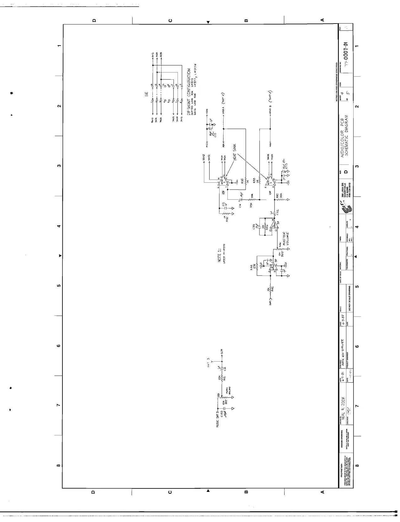
- Summing Amplifier and Master Volume Control (3F, R46)
One segment of Operational Amplifier 3F is used here as a point at which all the various sounds generated on this PCB are brought together. Note that the output goes immediately to a 10K POT (R46) which has ground on the other end. The wiper, therefore, varies the final output volume of all sounds together.
- Integrator and Audio Power Amplifier (3F,10F)
Another segment of Operational Amplifier 3F is used here as an integrator; that is, it is used to “roll off‘ the higher frequency sounds in order to prevent the power amplifier from going into unwanted oscillation.
A-14 The Audio Power Amplifier (10F) is 'a Dual Audio Amplifier IC configured as a “Bridge Amplifier" and may be either a LM377 or LM378 for Revision A, Audio/Color PCB. Revision letters are located at position 11C. {n later versions of PEPPER II it may possibly use a LM379 with a reconfigured DIP shunt. Information regarding this is available in the operators manual for this game, or contact the Exidy Customer Service Department for assistance if you must use an alternate device.
Volume Controls
Master Volume R46, see the fourth page of Audio/Color PCB schematics.
Music Volume R9, see the fourth page of Audio/Color PCB schematics.
Special Effects Volume R3, see the fourth page of Audio/Color PCB schematics.
PAGE 5 OF
: AUDIO/COLOR PCB
- Pattern Character Color Division (10A,9A)
The two segments of Flip-Flop 10A, using the upper two address lines from the character generator circuit, divide the character generator RAM space into four (4) conceptual groups (or quadrants) according to address. This is done in order to assign different colors to different characters.
Using this method, any character stored ina particular quadrant will be the same color as any other character stored in that same quadrant. If the same character is stored in a different quadrant, it will be displayed with a different color. The output of 9A (Two-line to Four-line decoder) applies the separated video lines of these quadrants to Priority encoder 10B, whose task is to determine which image is to take visual preference when two or more coincide on the TV screen; that is, which image is to appear to be in the "foreground", and which is to appear to be in the ‘background’.
- Priority Encoder (10B)
All the video signals generated by the logic PCB are applied to the priority encoder. The signals assigned the higher priority are shown at the top, and the lower priority are shown on the bottom. The output of this device is a 3 Bit code representing the highest priority video line active at that instant. This output code is then sent to the color multiplexers as an address which will select the appropriate color for the imagery generated on that video line. Note that the lowest priority input to the encoder is tied permanently low (active). This insures that when no other video is being generated, there is a background color present, unless of course, the program has selected a background color of black at that time.
- Color Data Latches (11C,12C,13C)
These latches are addressed directly by the Logic PCB microprocessor. Here the microprocessor stores the data that determines which character is what color. This data is then passed to the color selection multiplexers.
- Color Selection Multiplexers (11B, 12B, 13B)
Each of the three multiplexers controls the video output to a different color gun in the CRT. One turns the red gun on or off, one turns the green gun on or off, and the third does the same for the blue gun. The output combination of the three multiplexers provides for one of eight possible colors to be displayed at any given instant. The color displayed is determined by two things: what type of video is present (e.g. which character), and what color the microprocessor has currently assigned to that type of video. As mentioned above, the color assignations are stored in the color data latches. The priority encoder (10B) issues the code representing the type of video currently displayed. Using these two pieces of information, the multiplexers look at the appropriate bits in the color latches and send the data directly to the TV to turn the color guns on or off.
- Video and Sync Signal Polarity Selection (11A,12A)
Before being reclocked one last time, all video outputs are passed through an Exclusive-Or gate (11A), so that one input of each segment can be used to invert the video (make it 180 degrees out of phase with respect to the input to the gate). This feature insures compatibility with TV monitors made by several different manufacturers.
The TV Sync signals are also routed through Exclusive-Or gate segments (12A) for the same purpose.
- Final Video Output Re-synchronization (13A)
To insure that all video signals and sync signals are accurately synchronized in time, they are all re-clocked one last time together by a HEX ‘"D"Flip-Flop. It “cleans up" any spurious irregularities or propagation delays that may have crept into any of the video or sync signals.
PART II: ILLUSTRATED PARTS LIST FOR PEPPER II™
The following is an illustrated parts list to aid you, should you ever need to order new parts for PEPPER II". The drawings have all parts labeled by a number within a circle. This number refers to the item number on the Parts List directly across from the drawing. in the case of the Final Assembly list, the second drawing has numbers referring to the Final Assembly list found opposite the first drawing.
Following the illustrated Parts List is a list of parts for the Logic, Audio and Plane Interface boards.
A. PEPPER I1™ FINAL ASSEMBLY
Item Part Number
1 D38-5137-10 2 D90-0002-00 3 C38-5148-10 4 D38-5134-10 5 C38-5136-10 6 90-0035-00
11 38-5152-10
- 90-0005-00 13 C76-1225-20 14 £71-2443-10 15 71-2250-10 16 C71-2442-10 17 €38-5133-10 18 C71-2440-10 19 B68-0035~11 20 B68-0131-10 21 C80-0003-00
- C75-5185-11 23 €80-0002-00 24 C68-6050-20 25 C68-0124-10 26 B68-0142-10 27° C68-0141-10 28 83-0001-00 29 BB9-1019-10 30 B89-1020-10 31 B89-1021-10 32 80-0004-00 33 80-0005-00 34-70-6053 35 72-3000 36 68-6050-10 37-74-6524 38 74-8532 39-74-4601 40 74-4606 41-74-5464 42-74-8534 43-74-8544 44 74-5468 45 74-6513 46-74-6506 47 63-7061 48 88-4002 49 87-1001 50 87~1062 51 00-0001-00
53 33-5040 54 89-1009-10 55 74-4603 56 75-5198 57 74-8549 58 89-1023-10 59 82-1019-10 60 36-0006-00 61 36-0005-00 62 77-0006-00 63 51-6047-01 64 58-6070-65 65 55-6000-01 Description
Assy, Cabinet Assy, Control Panel Assy, monitor Assy, Universal Power Supply Assy, !solation transformer Assy, Coin Door 25 cents
Assy, Flourescent Light Assy, Logic and Audio Color Board Assy, Door Assy, Main Harness Assy, Isolation Transformer Harness Assy, Speaker Harness Assy, Power Cord Ground Cable Oblong Speaker Grille lamp bracket Logo Plex Ambient shieid Display Plex Coin box lid Mounting Bracket, Logo Plex Panel Hasp, Coin Box Interlock Switch Bracket Labe!, Serial No. Chrome/Mylar Label, Fuse Label, Voltage, 110V Label, Voltage, 220V Decal, Side art, left Decal, Side art, right Light, Flourescent bulb Switch, Interlock Coin Box, Universal #10-24 x 1 1/2" large carriage black #10-32 x 1° Ig. soc. button head black #8 x 5/8" Ig. pan hd, x-recessed type AB #8 x 1° Ig. flat head x-recessed type AB #8 x 1/2" |g, sheet metal, type AB, pan head, square drive, Black #10-24 x 2" Ig. hex hd. mach #10-24 x 1° Ig, carriage, Blk #10 fender washer, 7/32" ID x 1 1/4*OD #10-32 kep nut #10-24 kep nut speaker small! tywrap, 4" minature packing list envelope plastic bag, 10" x 12* Pepper Op and Service Manual
TV Manual, Wells-Gardner #19K 4605 FCC Warning Label #8 X 3/4" |g, pan hd, x-rec, type AB zinc pit Retainer clip (flour.) #10-24 x 1 1/4, carriage bolt black Static Display Seal, Strain Relief Plate Plane Interface Ribbon Cable Assy Plane Interface Ribbon Cable Assy PCB Plane Interface #6 3/4", wood screw spacer, nylon 1/8" lg washer #6 flat
B-2
B. CONTROL PANEL ASSEMBLY 90-0002-00
Item Part Number Description
1 65~-0001-00 2 80-0001-00 3 90-0001-01 4 B68-0140-10 5 94-0001-00 7 74-0203 8 72-3062-11 9 72~-3061-11 10 74-5247 1 53-0042-01 12 74-8548
European Version: 90-0001-02 94-0002-00 CONTROL PANEL FAB POLYCARBONATE OVERLAY . JOYSTICK ASSY LATCH BRACKET CONTROL PANEL HARNESS ASSY PAL-NUT PUSH BUTTON SWITCH ASSY 10-24 X 5/8" CARRIAGE BOLT, BLK.ZN 10-24 NYLOCK NUT #6-32 X 3/8" LARGE FLAT HEAD, X-REC., MACHINE ZINC PLATE
JOYSTICK ASSY CONTROL PANEL HARNESS ASSEMBLY
C. JOYSTICK (90-0001-00)
(Part Numbers included on drawing, opposite this page)
D. UNIVERSAL POWER SUPPLY ASSEMBLY, 90-0006-00
Item Part Number
CON AUK
= ° €76-1258-10 74-3503 74-2516 74-5198 74-3500 74-3502 78-3001 63-4028 77-0009-05 C71-2389-10 71-2255-10 80-4004 88-4002 Description POWER SUPPLY MOUNTING BOARD SCREW, PAN HD, #6 X 1/2" LG. TYPE AB SPACER, #6 x .125 NON-METALLIC SCREW, PAN HD. #6-32 x 3/4" LG. . WASHER, FLAT, #6 NUT, KEP, 46-32 POWER SUPPLY, 5V @ 6.0 AMPS TRANSFORMER, FILAMENT, 24V @ 4.0 AMPS . PRINTED CIRCUIT ASSEMBLY UNIVERSAL POWER SUPPLY HARNESS, POWER SUPPLY HARNESS, POWER SUPPLY FLOURESCENT 1/4" SHRINK TUBING TYRAP
E.
Item Part Number
CeENauawna aaa wNad Description
63-4029 B76-1259-10 74-5463 74-5468 74-6402 74-6506 61-8058 61-8055 61-8357
74-8536 61-8072 61-8054 TRANSFORMER, | SOLATION ISOLATION TRANSFORMER ASSEMBLY, C38-5136-10
BOARD MTG. TRANS SCREW, PAN HD. WASHER, FENDER, #10-24 X 1.00" LG #10 WASHER, FLAT, #10 NUT, KEP, #10-24 3 PIN MOLEX PLUG FEMALE MOLEX PINS 2 PIN MOLEX RECEPTACLE WIRE, COPPER, STRANDED #18 AWG #10 STUD TERMINAL, RING SPLICE, BUTT MALE MOLEX PIN
F. COIN DOOR ASSEMBLY, 90-0003-00
Item Part Number Description
90-0032-00 COIN DOOR, MODIFIED 90-0031-00 COIN ACCEPTOR- MODIFIED 74-3502 NUT-KEP #6-32 71-2444-10 UNIVERSAL COIN HARNESS ASSY RW
G.
ONAUVAWNA LOGIC AND AUDIO BOARD ASSEMBLY 90-0005-00
77-0008-05 77-0007-05 74-8552 74-5182 36-0006-00 74-5173 36-0005-00 77-0006-05 PWA LOGIC PWA AUDIO COLOR SPACER NON-METALLIC #6-32 X 7/8 LONG SCREW, PAN HD, PHIL #6-32 x 1/4 LG CABLE ASSY, RIBBON, 14 PIN WASHER, FLAT, NYLON #6 PLANE INTERFACE RIBBON CABLE PLANE INTERFACE PCB ASSEMBLY
H. PRINTED CIRCUIT ASSEMBLY-UNIVERSAL POWER SUPPLY, 77-0009-05
1 77-0009-04 2 13-4085-00 3 13-3364-00 4 13-6844-0 5 20-0003-00 6 20-0005-00 7 21-0003-00 8 ~ 21-0004-00 9 21-0005-00 10 21-0006-00 11 84-0012-00 12 84-0013-00 13 40-0002-00 14 50~-4027-00 15 53-4011-01 16 37-0001-00 UNIVERSAL POWER SUPPLY BOARD CAP, ELECT. 4000MF, 50V AXIAL LEAD CAP, ELECT. DIP 33MF 25V + 20% CAP, ELECT. DIP 6.8MF 25V + 20% DIODE 6051 or UT4010 RECTIFIER, BRIDGE MDA-970~1 TRANSISTOR, 2N3055 TRANSISTOR, 2N6246 REGULATOR 7905 REGULATOR 7912 HEATS INK HEATS INK CONNECTOR 12 PIN (WAFER HEADER) SCREW, PAN HD #4-40 x 3/8 LG (PHIL) NUT, KEP #4-40 TYRAP 5 1/2"
- LOGIC BOARD, 77-0008-05
[tem Part Number
77-0008-04 22-0001-02 22-0002-02 22-0003-02 22-0004-00 22-0005-02 22-0006-02 22-0007-02 22-0008-02 10 22-0009-02 1 22-0010-02 12 22-0011-02 13 22-0012-02 14 22-0013-02 15 22-0014-02 16 22-0015-02 17 22-0016-02 18 22-0017-02 19 22-0018-02 20 22-0019-02 21 22-0020-02 22 22-0021-02 23 25-0004-00 24 28-0004-00 25 24-0011-00 C@OVNAUAWNA
26 24-0012-00
27 24-0013-00
28 20-0001-01 29 02-4712-00 30 02-1222-00 31 02-1822-00 32 02-2222-00 33 02-2722-00 34 09-0007 -00
35 09-0004-00
36 09-0008-00
37 09-0009-00
38 23-0045-00
39 10-1034-1 Description
PCB LOGIC 1.C. 74LS00 1.C. 74LS02 1.C. 74LS04 1.C. 7407 1.C. 74LS08 1.C. 741811 {.C. 74LS20 1.C. 74LS21 1.C. 74LS27 1.C. 74LS32 1.C. 74874 1.C. 7418112 1.C. 74LS138 #.C. 7418139 (.C. 7418157 1.C. 74LS161 1.C. 7418166 \.C. 7418193 1.C. 74LS241 1.C. 7418245 1.C. 7418374 MICROPROCESSOR 6502 2114 RAM (1K x 4) 6301 PROM (256x4) P2L5C-1 6331 PROM (32x8) P2L6D~-1 6331 PROM (32x8) HRL14H-1 1N4002 DIODE RES. 470 OHM 1/4W 5% RES. 1.2K 1/4W 5% RES. 1.8K 1/4W 5% RES. 2.2K 1/4W 5% RES. 2.7K 1/4W 5% RES. 220 OHM 1/8W 5% 10 Pin Sip RES. 2.2K 1/8W 5% 10 Pin Sip RES. 4.7K 1/8 5% 10 Pin Sip RES. 6.8K 1/8W 5% 10 Pin Sip CAP. .O1uf CERAMIC DISC CAP. Disc «luf CERAMIC Location
3D, 15C, 15H 4H, 6H, 8F 1D, 4D, 3F, 10F, 11F . 2c 5E 3H ' 2F 12F, 15 7F, 2H 6F 1c 2E, 6E 5B, 5D 7E, 16H 14A, 14E 1E, 2D, 4F, 5F 12B, 12D, 13D, 14D, 150 10E, 12E, 13F, 15F, 14FM 16F, 11£ 13E 1A, 3A, t5A, 3B, 6B, 9B, 8C, 7D, 9E, 4H 3C, 4C, 6C, 13B, 15B 1F, 14B, 7C, 9D, 8E 2A 4A, 5A, 7B, 8B 5C
6D
44H
BE, 9F, 2H 1D, 2H 2c 1c, 2c 7E, 2A 1C, 2C 9E
14A
1D
A/R
- LOGIC BOARD, continued
Item Part Number Description
40 10-1044-1 41 13-6844-1
42 13-3365~-0
43 13-4775-0
44 47-0001-00 45 49-5002-00
46 29-0001-00 47 40-0061-00
48 44-1601-00
49 44-2401-00
50 44-4001-00
51 44-1401-00
52 44-1801-00 53 11-1053-00 54 02-2212-00 55 02-1802-00 56 23-0050-03 57 23-0051-03 58 23-0052-03 59 23-0053-03 60 10-2214-4 61 23-0054-03 62 23-0055-03 63 23-0056-03 64 23-0049-00 CAP. 6.8uf 25v DIPTANT 1C, CAP. 33uf 25V ELECTROLYTIC CAP. 470uf 10V ELECTROLYTIC DIPSHUNT JUMPER PAKS 16 PIN DIP SWITCH 8 POS. CRYSTAL 11.289mhz (SERIES) 10 PIN MALE MOLEX HOR DIP SOCKETS 16 PIN LOW PROFILE DIP SOCKETS LOW PROF ILE DIP SOCKETS 40 PIN LOW PROFILE DIP SOCKETS LOW PROFILE DIP SOCKETS 18 PIN LOW PROFLE CAP 1uf DIPTANT RES. 220 OKM 1/4W 5% RES. 18 OHM 1/4W 5% CAP. 330 pf CER. DISC E PROM, 2732 P2L6A=1 £ PROM, 2732 P2L7A-1 E PROM, 2732 P2L8A~1 E PROM, 2732 P2L9A-1 CAP 220 E PROM, E PROM, E PROM, E PROM, 24 PIN
14 PIN
2732 P2L10A-1 2732 P2L11A-1 2732 P2L12A-1 2716 P2L11D-1
J AUDIO/COLOR BOARD ASSEMBLY 77-0007~-05
77-0007-04 22-0013-02 26-0003-00 25-0002-00 25-0004-00 27-0001-00 22-0022-02 27-0002-00 22-0023-00 Qo 22-0055-00 POON OUFUYN A PRINTED CIRCUIT BOARD 1.C. 74LS138 1.C. 6520 (.C. 6532 1.C. 6502 1.C. 6840 1.C. 74LS154 {.C. 8253 1.C. 4069 1.C. 4013B Location
15D, 1c, 2c 6E, 13F
10H
4B, 11B, 10D
16A 1D
16C, 16F 4B, 11B, 14H, 10D 6A thru 13A, 11D 5C, 6D
2A
4A, 5A, 7B, 8B, 11C 12C, 13C, 14€ C45 thru C52, 5D, 2H R200, R311 R300 thru R302 5D 6A 7A BA 9A pf CERAMIC DISC 10A WA 12A 11D
13D 8B, 9B 7B 3B 3D 4B
1A 1B
J- AUDIO/COLOR BOARD ASSEMBLY, continued
Item Part Number Description
1 22-0003-02 12 22-0001-02 13 22-0021-02 14 22-0024-00 15 22-0025-00 16 22-0056-00 17 22-0011-02 18 22-0026-00 19 22-0054-00 20 22-0027-02 21 22-0028-00 22 22-0014-02 23 22-0057-00 24 22-0029-02 25 22-0030-02 26 22-0031-02 27 10-1044-1
28 10-2204-1 29 10-1034-1 30 13-3365-1
31 13-1075-00
32 13-4755-00
33 13-1055-00
34 02-1822-00 35 02-3322-00 36 02-1022-00 37 02-1062-00 38 02-3012-00 39 02-1042-00
40 02-2232-00 41 02-1052-00 42 02-3332-00 43 02-2722-00 44 02-2732-00 45 02-1322-00 46 02-6812-00 47 02-3312-00 48 02-1612-00 1.c. 1.C. 1.c. 1.c. 1.C. 1.C. i.c. men 1.C. 1.C. 1.c. {.C. men 1.C. 1.C. 1.c. 74LS04 74LS00 7418374 4053 4175 4562 7ALS74 1M324 7406 74LS86 4051 74LS139 M377 74LS148 74LS151 74LS174 Location
5D 6B 1C, 11C, 12C, 13€ e 2D, 4D 6E, 73, 8E, 9E 5E ‘ 10A, 6D 3F, 2E
11A, 12A, 4E 7D, 8D, 9D 9A 10E 10B 11B, 12B, 13B 13A +1 uf. CERAMIC CAP 25V 1A thru 7A, 9A, 11A, 13A, 1B, 6B, 9B, 118, 1C, 11C,
22pf CERAMIC CAP 16V. 01 uf CERAMIC CAP 16V 33uf CAP, 25V, ELECTROLYTIC W/AX1AL LEADS 100uf CAP ELECTRO- LYTIC 16V 4.7uf CAP ELECTRO- LYTIC 16V 1.0uf CAP ELECTRO- LYTIC 16V 1.8K RES. 1/4W 5% 3.3K RES. 1/4W 5% 1K RES. 1/4W 5% 10M RES. 1/4W 5% 300 OHM RES. 1/4W 5% 100K RES. 1/4W 5%
22K RES. 1/4W 5% IM RES. 1/4W 5% 33K RES. 1/4W 5% 2.7K RES. 1/4W 5% 27K RES. 1/4W 5% 1.3K RES. 1/4W 5% 680 OHM RES. 1/4W 5% 330 OHM RES. 1/4W 5% 160 OHM RES. 1/4W 5% 13C, 1D 3D, 5D, 7D, 9D, 11D, 13D, 1£, 2E, C7, C9, C10, 3E, 5E, 7E, 9E, C12, 136, 2F, 4F, 12F, 9E, 2E, 3F C1 C6, C8, C11, C33, 1C C13, C15, C17 thru c21
C16
C3, C4, C5
C27, C32, C2
R3, R4, RS R6 R14 R2 R1 R10, R11, R12, R27 R47, 428, R29 R15, R30 R32 R33, R35 R34 « R21 RA4 R26 R19 R7, R25 RB, R24
J. AUDIO/COLOR BOARD ASSEMBLY, continued
ttem Part Number Description
49 02-8202-00 50 02-3902-00 51 07-1032-00 82 OW RES. 1/4W 5% 39 OK RES. 1/4W 5% 10K RES. 1/4W 5%
| 52 | 07-0004-00 | 10K POT |
| 53 | 09-0008-00 | 4.7K RES. PAC 10 PIN |
SIP
| 54 | 29-0002-00 | 3.579545 MHZ CRYSTAL |
| 55 | 47-0001-00 | 16 PIN DIP SHUNT |
| 56 | 44-1401-00 | 14 PIN DIP SOCKET |
| 57 | 44-2401-00 | 24 PIN DIP SOCKET |
| 58 | 44-2801-00 | 28 PIN DIP SOCKET |
| 59 | 44-4001-00 | 40 PIN DIP SOCKET |
| 60 | 44-1601-00 | 16 PIN DIP SOCKET |
| 61 | 13-4735-00 | +47 uf CAP ELECTRO- |
LYTIC 16V 10 PIN MALE CONNECTOR 10 PIN FLAT CABLE ASSEMBLY 62 40-0005-10 63 37-0009-00
| 64 | 75-0006-00 | HEATSINK STAVER V7-1 |
| 65 | 23-0048-00 | E PROM 2716, P2A3A=1 |
| 66 | 23-0047-00 | E PROM 2716, P2A4A-1 |
67 23-0046-00 68 41-0003-00 E PROM 2716, P2A5A~-1 FEMALE 10 PIN
K. PLANE INTERFACE BOARD 77-0006-05
Part Number Description
77-0006-04 PLANE INTERFACE BOARD 10-1044-1 +1UF CAP., 25 VOLT 22-0001-02 1.C. 74LS00 22-0017-02 1.C., 74LS166 22-0020-02 1.C. 74LS245 23-0045-00 1.C., 6116 44-1401-00 14 PIN SOCKET 44-2401-00 24 PIN SOCKET Location
R20 R22, R23 R16, R17, R18, R42, R45 R9, R31, R46 4D
2A 8A, 11E J20, 1A, 1B, 5E 3A, 4A, 5A, 6A, 7A, 2B 3D 3B, 2D, C14 7B, 8B, 9B 4D, 8A, 11E, 6E- 9E, 7D-9D
P21 J2, J3
ONLY W/ M277, LM278 5A 6A 7A
mae
i]
marl WARNES, Je Poa
ro. Logie Boarts ores UNLESS Ormamace sreCrED 13
=F
AVDiej/couoR Pee SCHEMATIC. CIAGRAM es | I 2 I 1 | 717-0007-01
This page is a drawing, shown as the original scan.
a a as 5A 7
we sae fon
PROGRAM MEMORY
ea L T F-09071 ] 1
‘DESCRIPTION ‘Ae REVISED PER ECN 100235 17-30-61
lor +12V (HI)
1, ALL CAPACITOR VALUES ARE IN MICROFARADS
NOTES UNLESS OTHERWISE SPECIFIED:
ELECTRICAL SCHEMATIC, [DIDIUERSAL POWER SUPPLY ZA SHOWN FOR REFERENCE ONLY +12V (Lo) —12V (Lo) —12V (HI) tow
TOLERANCES
a | z | £ | v . §
wyadyid OLLWW3HOS ad _YOT02/oIGNv 10-4000 -«e
ow 508 sey von ry BO. by 50" any 1 rey HE
| sy a
Le oa
G07-CBO) 00-4147204
This page is a drawing, shown as the original scan.
14 Pit DIP SOCKET CouvECTER ABD: ts ye vives marry AT So" e = D
r
g EGeonel h we alg]
c ween Gh ath Bm a> _esywen ——~Te aw scsynic A LI
RA ° syne _T) 2 HSYNCA
ist 7 vewe__Ta})
PATTERN) CIRRACIER CoLar DIVISION
yDyAto weco y
a ECRERORUSaEE!
ry PRIORITY ERcaDER
10 FIN WAFER HEADER
ourpur Te
TV mOMtTOR Cmey mat
HARNESS )
REDA
cRNA ELUA csvNcn HSWACA VSYNCA RED our, SN Our BLO our csyic_6oF SYNC ovr VEYNC QUT
fsa amenuser
sscux I
FUDIO/@LoR PCB ScheMATIC. DAGeAm
This page reads as a drawing: its text was drawn rather than typeset, and comes out in fragments. See the original scan.
BLU (xn) 2 NIOD. UNLESS TOLERANCES OTHERWISE SPECIFED
races.
x wor | wm
xx USED ON) XXX LT: 2444 Jo [VENTURE [Tincies
a
GRN 1 HOSW ais J peat GRN NOD ON WOD ON
2 HORN 2s
¥ALNNOO NIOO > ec OX Q? ZO ae Dz gay LHM/8 nyo/nna
wE {° ie)
¢s HOLIMS WTS
INDOOR” HARNESS WIRING? 91 DIAGRAM - UNIV. eco 71-2449 40 !
B
DO NOT SCALE DRAWING
240) 9402. 2403, RED OUT GREEN OUT BLE SUT. AAA
mw DEFLYOKE WELLS GARDNER
ld «we K4901B, K4906B, K49518 5833
- K4956
WS/2 OF Cons Done © iimay tous D002 exe 0)
z Wore > &
ae
ae hers lsr Sze 7H. 98-000!-00
*
z | | zahow ananigze © ny eeaes (E) wgeiey © @
aaa Se SA QUIBER TWN } io} ‘
Ie)
- G0) ® J L.
vs onto eon) . Gey (or) Lawes 4, _| = eupeee vow foes FE, Fised Airis siren on Mime Riu Derbere wun Cee, Eeadteete Sie Kaations OC onee Genes “ooes
Dele Chse ea eerie OF er ie Bie Berpareys Liem ay, erm Dues, Sire Ae Ae ype fete BOGS ails init be saeieee Avene” Meee oy: Benton sien cheup Coane bute able curhiniints, Coieeh Bivbtes tabueies tb BE. Jee Rebhee Cage RE mci oe Fae BEEBE Bly RAED OLB EAB CRE Sole CEES So Cieeee oo fee eas CS aioe sorters, Sine Be ceene ¢ tie Oe Bs Benda. reer, O8 ee 3 2 ] 1
4 3 y 2 1
VEESION MCEO SWITCH USED nevesrone -Ol Guia 48-5013 00 miekoswirth -MmooiFiet) on aa one — D -02 nm1eTAE /0(3)A 250v (Eoperin) D Vv
CHner| MCEO SUNTAN %-01-00| JOr STICK (TEM | PART NUMBER ‘DESCRIPTION ir
oo: ee 2. py 390 JAVA DR thy ee ee 300 JAVA DR sons
° 2 & Y
/ ~
7a oie ag A 2 | NOTES UNLESS OTHERWISE SPECIFIED THIRD ANGLE | MACHINE PROJECTION | FINGH TE ASSEMBLY - TBY STICK. A Bl" | 4o-0c01-xx SCALE mT HT
4 3 a
$¢200] N29 ue. a9SINIY
a
S) “9isa0 43u 1s LNANOdWOO
“ON WALI
APPLY HEAT TRANSFER COMPOUND FOR PARTS LIST SEE 77-3365 ~- 15 TO ITEMS 7 THRU It
NOTES UNLESS OTHERWISE SPECIFIED:
[UNIVERSAL POWER SUR PCB _BSSY eee a I timo 77-3365-15 Paar as rom eas, DO NOT SCALE DRAWING onan ry
REVISONS ESERIPTION DAE 1 _7 |B [RevseD PERECN 100235 (8/4/81
C [REVISED PER ECN 100240
230 VAC 3 (3)
5 ) (3x)
MLMBER, REFERS TO (ISOLATION TRANS FORMER ASSY PARTS CIST (TEM
BLK/GAN RED busied —
= | i BLK a t GAN Sa = Wit BLK/RED 5.00 5.00 370 Min —————>»} | —<— 27.0 MIN-————>|
14.50 __ | 368,30 INCH TOLERANCES UNLESS. iced crrenoe seed ST wees | ven [ @) a] x EYE
xx [#50 [ben pésivisio fyentuRe |}
1S VAC
NOTES UNLESS OTHERWISE SPECIFIED. FOR PARTS LIST 38-5136-XK peerscnre" TRANSFORMER || ASSY, ISOLATION
DO NOT SCALE DRAWING le] c vr if hfe
DESIGN DRAWING. WinreNnecuse A TOLERANCES
This page reads as a drawing: its text was drawn rather than typeset, and comes out in fragments. See the original scan.
i #
’ .
: ¢
REORDER NUMBER: 00-0002-00