Black Widow SP-234 2nd Printing
Black Widow (Atari, 1982) · Schematic Package · 23 pages · 79 sections · original scan
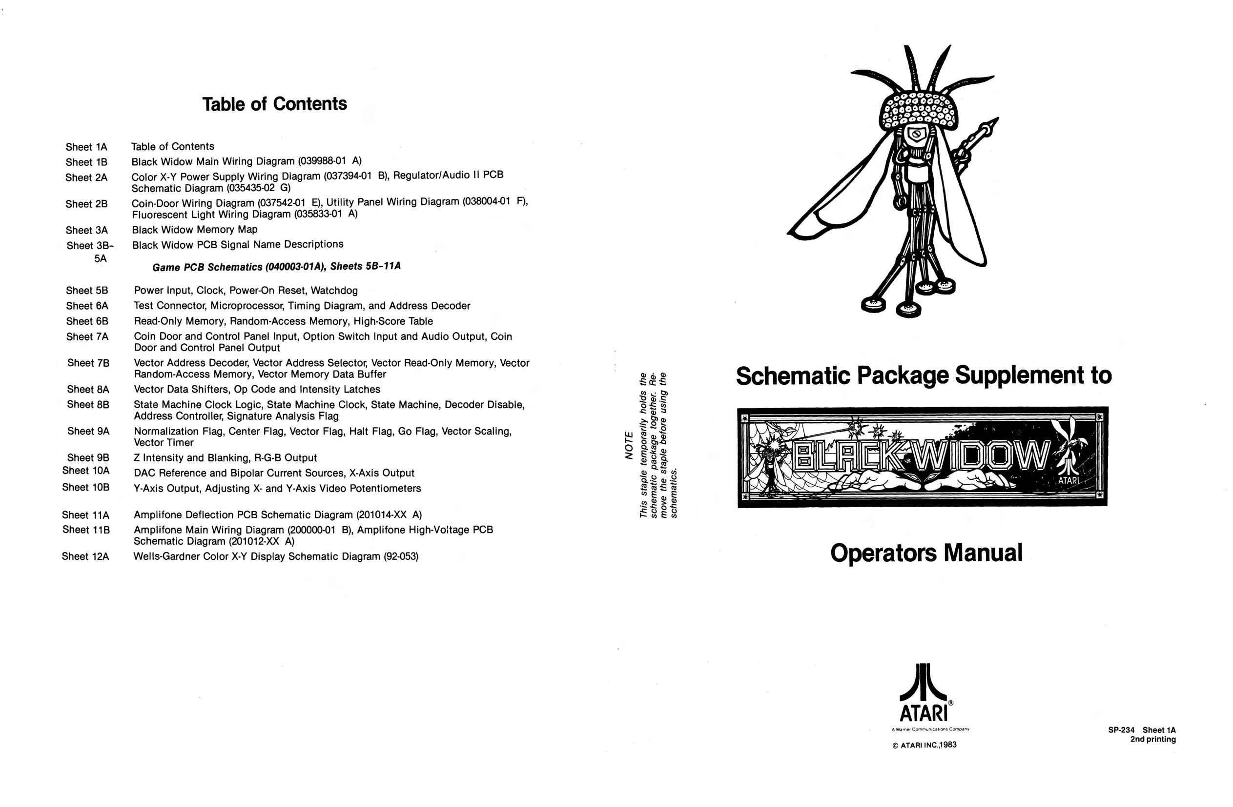
Sheet 1A Sheet 1B Sheet 2A
Sheet 2B
Sheet 3A Sheet 3B- 5A
Sheet 5B Sheet 6A Sheet 6B Sheet 7A
Sheet 7B
Sheet 8A Sheet 8B
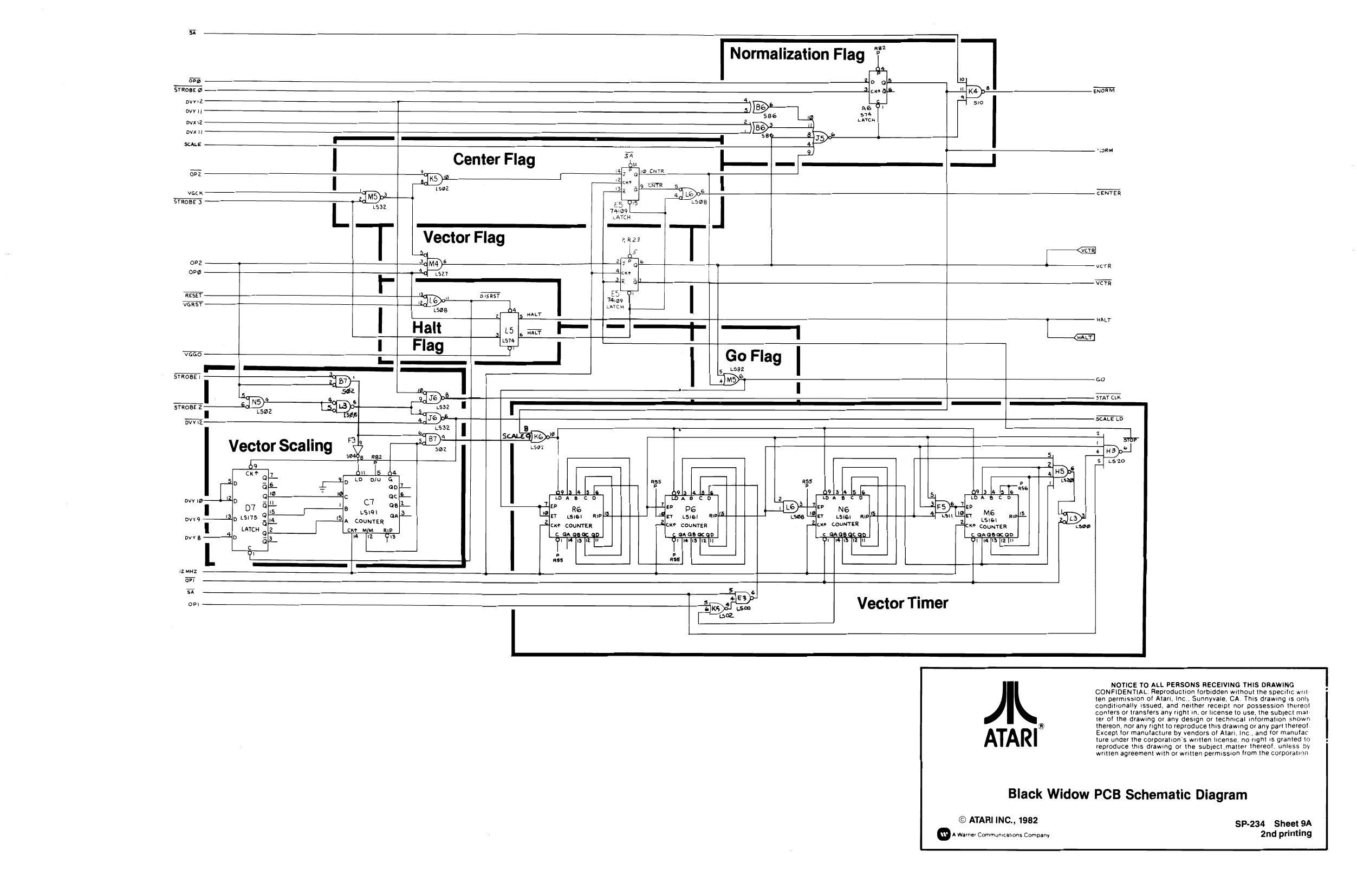
Sheet 9A
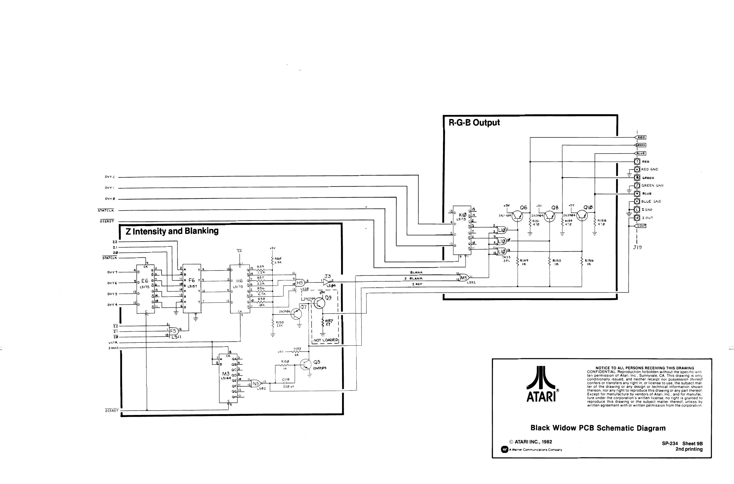
Sheet 9B Sheet 10A
Sheet 10B
Sheet 11A Sheet 11B
Sheet 12A Table of Contents
Table of Contents Black Widow Main Wiring Diagram (039988-01 A) Color X-Y Power Supply Wiring Diagram (037394-01 B), Regulator/Audio || PCB Schematic Diagram (035435-02 G) Coin-Door Wiring Diagram (037542-01 ), Utility Panel Wiring Diagram (038004-01 F), Fluorescent Light Wiring Diagram (035833-01 A) Black Widow Memory Map Black Widow PCB Signal Name Descriptions
Game PCB Schematics (040003-01A), Sheets 5B-11A
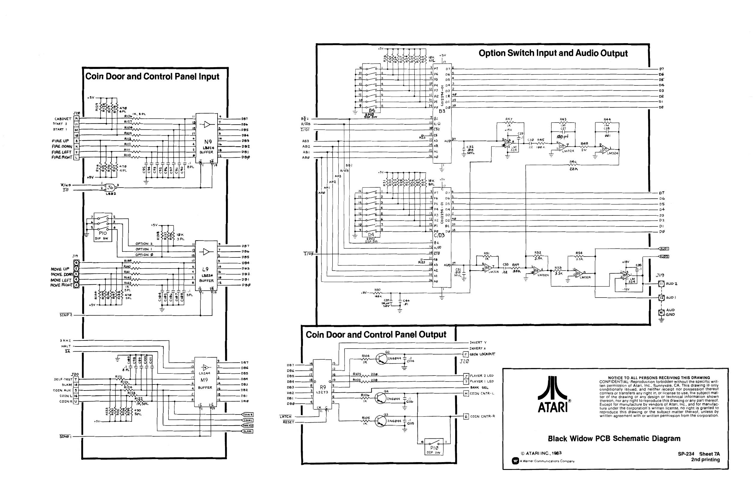
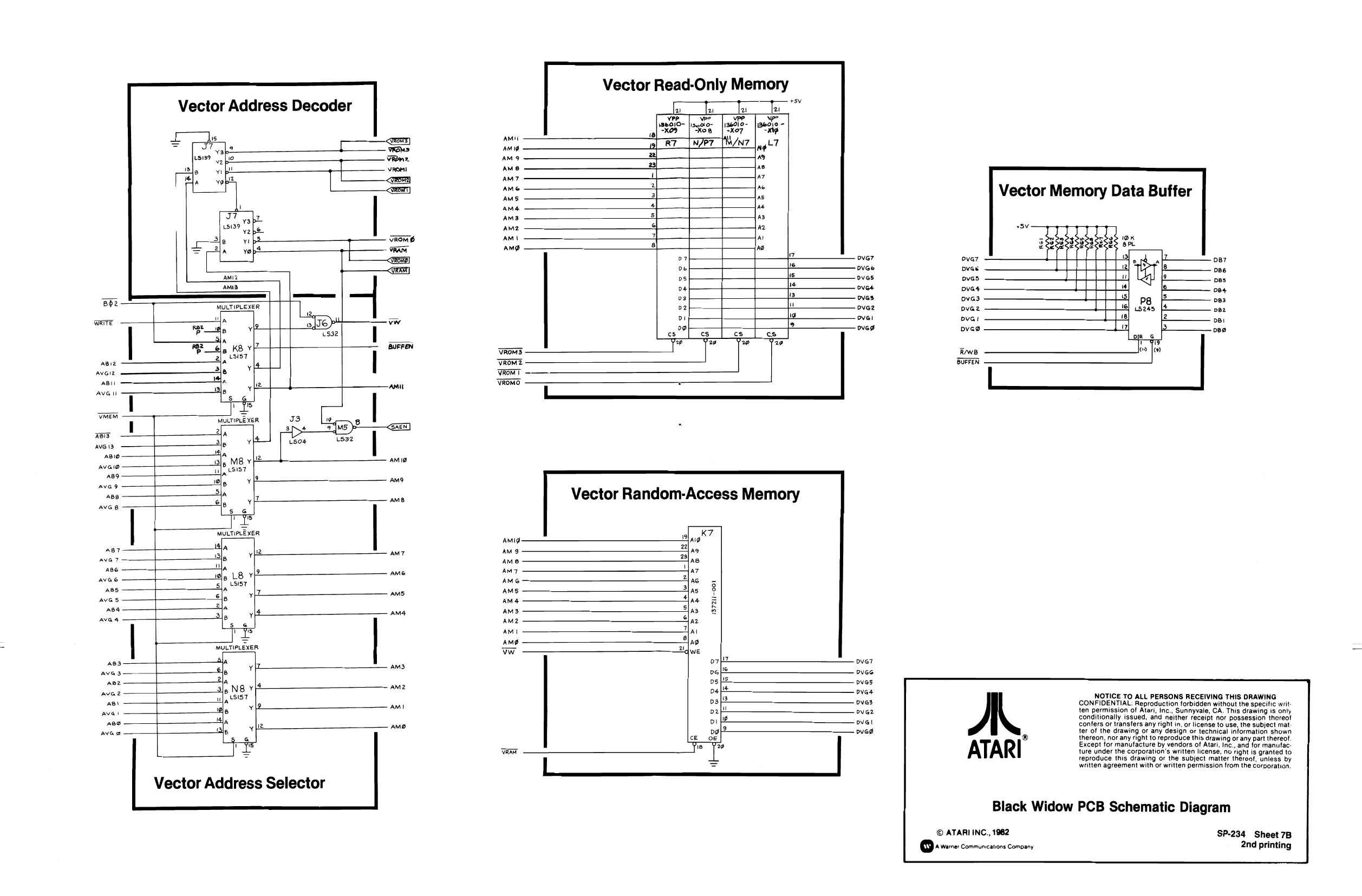
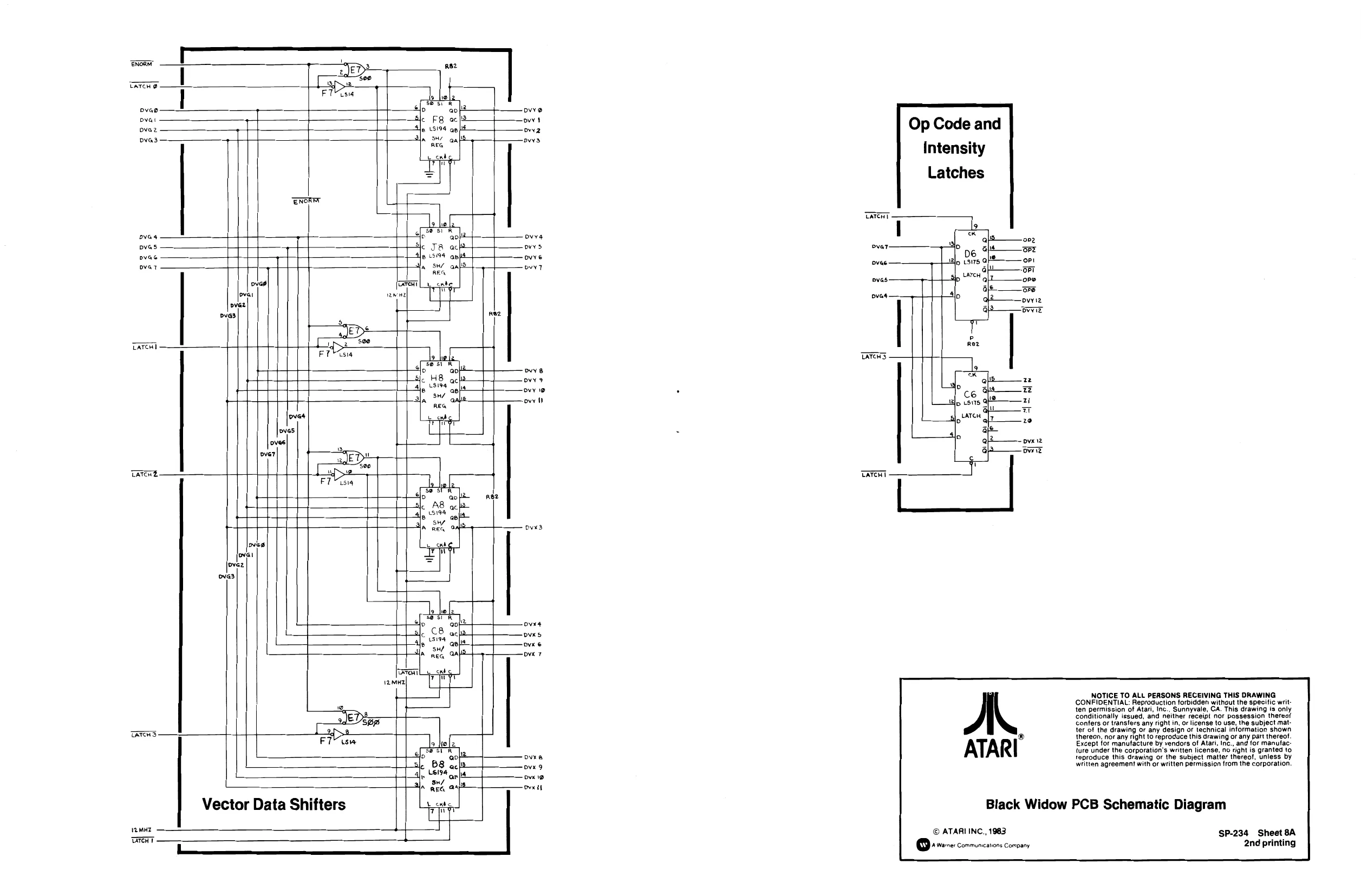
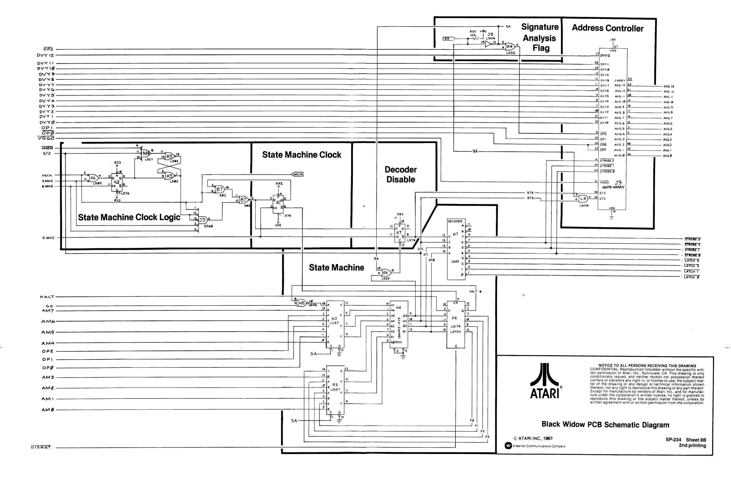
Power Input, Clock, Power-On Reset, Watchdog Test Connector, Microprocessor, Timing Diagram, and Address Decoder Read-Only Memory, Random-Access Memory, High-Score Table Coin Door and Control Panel Input, Option Switch Input and Audio Output, Coin Door and Control Panel Output Vector Address Decoder, Vector Address Selector, Vector Read-Only Memory, Vector Random-Access Memory, Vector Memory Data Buffer Vector Data Shifters, Op Code and Intensity Latches State Machine Clock Logic, State Machine Clock, State Machine, Decoder Disable, Address Controller, Signature Analysis Flag Normalization Flag, Center Flag, Vector Flag, Halt Flag, Go Flag, Vector Scaling, Vector Timer Z Intensity and Blanking, R-G-B Output DAC Reference and Bipolar Current Sources, X-Axis Output Y-Axis Output, Adjusting X- and Y-Axis Video Potentiometers
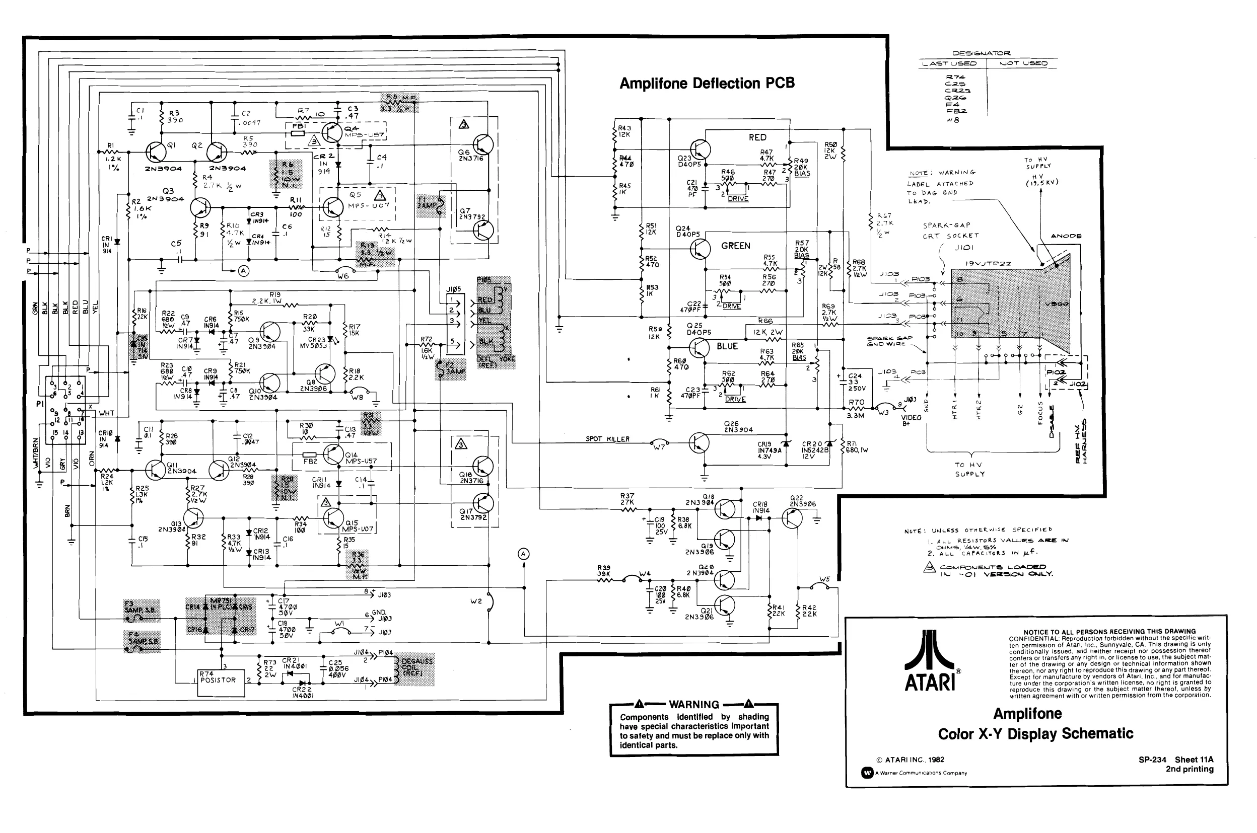
Amplifone Deflection PCB Schematic Diagram (201014-XX A) Amplifone Main Wiring Diagram (200000-01 B), Amplifone High-Voitage PCB Schematic Diagram (201012-XX A) Wells-Gardner Color X-Y Display Schematic Diagram (92-053)
schematics.
Operators Manual
AL ATARI ‘A Warner Communications Company © ATARI INC.1983 SP-234 Sheet 1A
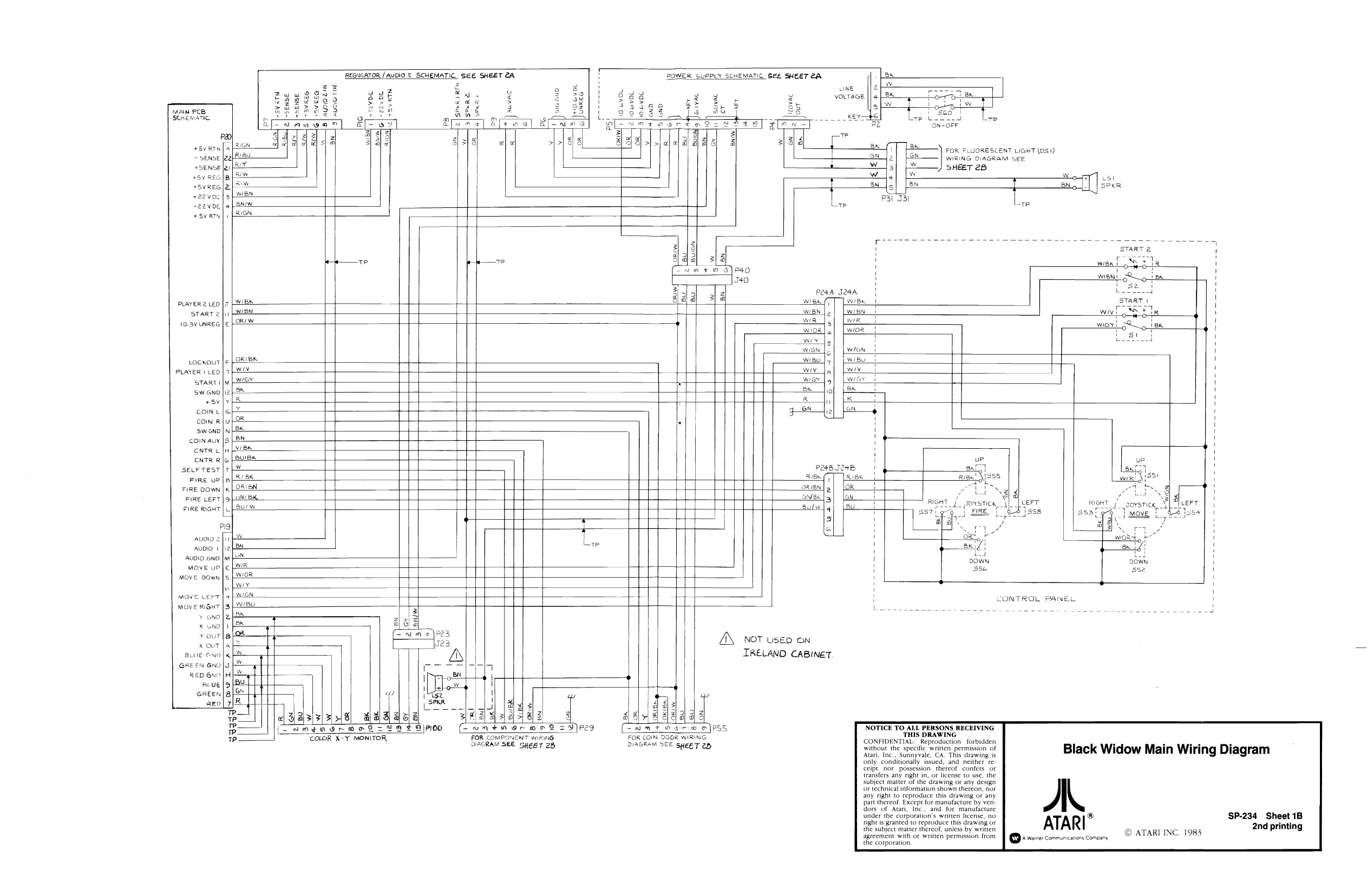
This page is a drawing, shown as the original scan.
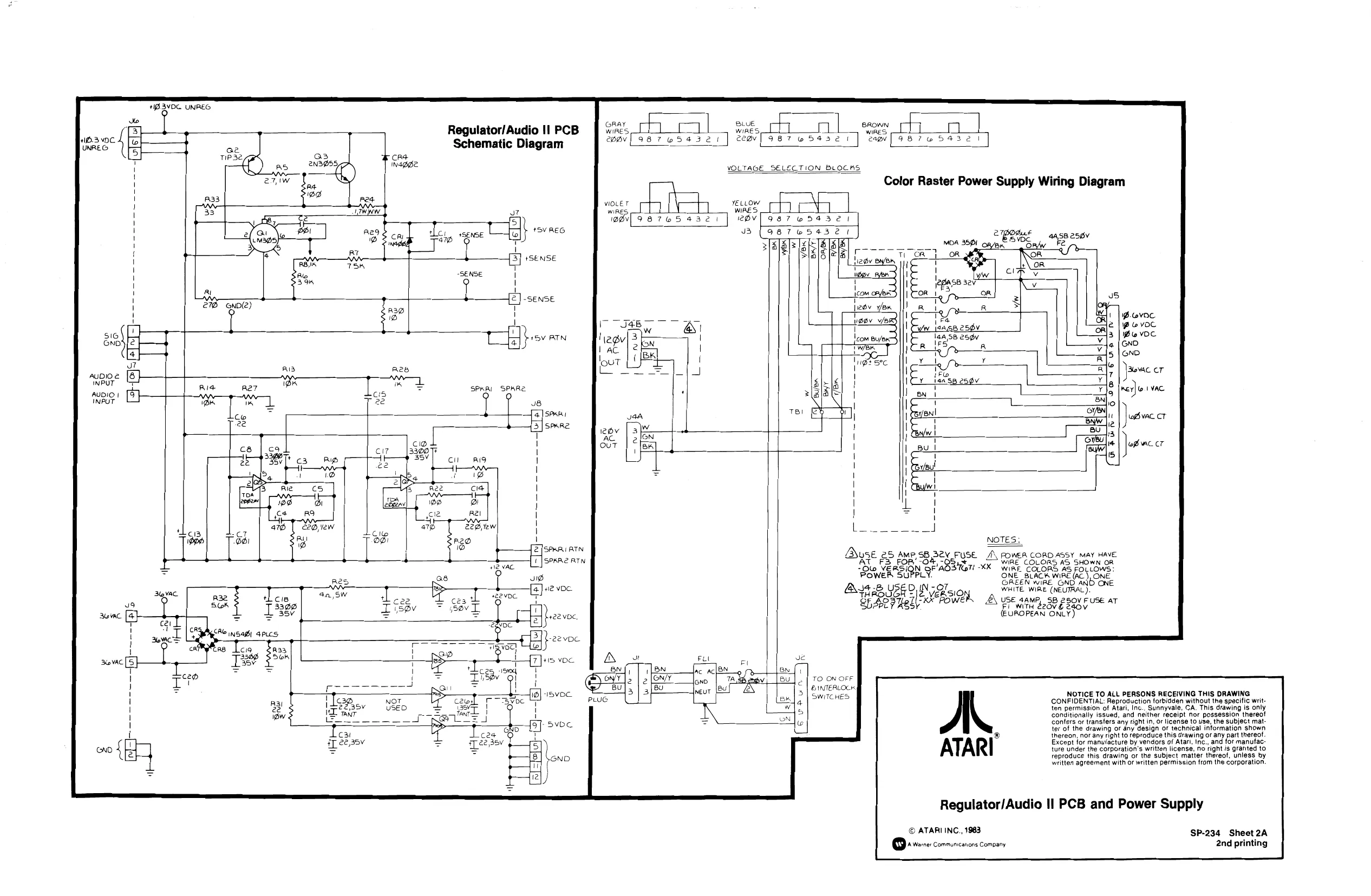
This page is a drawing, shown as the original scan.
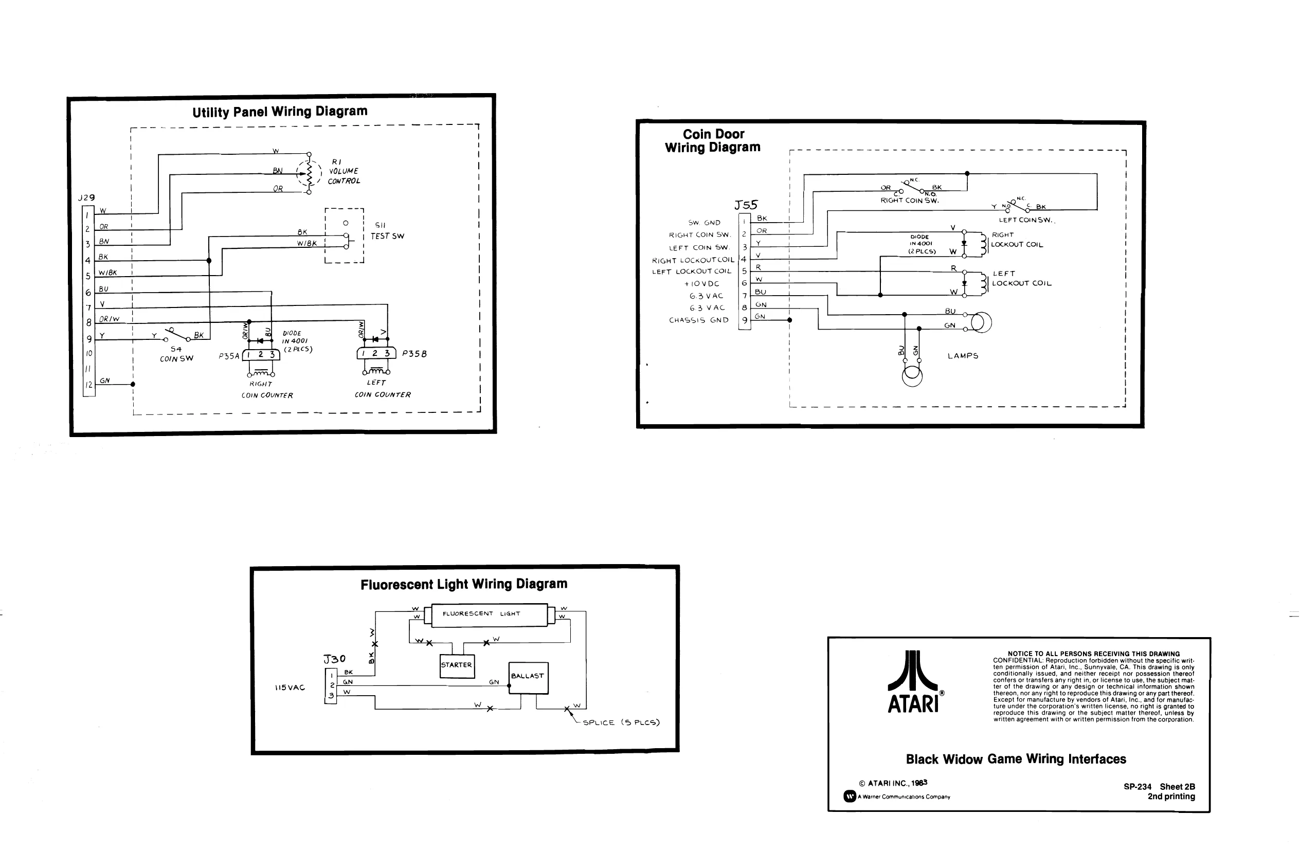
Utility Panel Wiring Diagram
Coin Door
Wiring Diagram
as
Jss " ss , Bk LEFT COINSW. TEST Sw RIGHT COIN SW OR an RIGHT a ¥ 'N 4001 [tocxour co LEFT COIN SW Coes, RIGHT LOCKOUT COIL R LEFT LOCKOUT COIL R Teer a 3 Ww. a S re)
si Sw. GND
+1OVDC LOCKOUT COIL
G3vac
63 VAC
CHASSIS GND aa een]
3| F3 >| im 4001 te =? 358
RIGHT Lerr
COIN COUNTER COIN COUNTER
Fluorescent Light Wiring Diagram
FLUORESCENT
confers or transfers any right in, or license to use, the subject mat- NOTICE TO ALL PERSONS RECEIVING THIS DRAWING CONFIDENTIAL: Reproduction forbidden without the specitic written permission of Atari, Inc., Sunnyvale, CA. This drawing is only conditionally issued, and neither receipt nor possession thereot
ter of the drawing or any design or technical information shown 5 VAC. thereon. nor any right to reproduce this drawing or any part thereof. ® Except for manufacture by vendors of Atari, Inc., and for manufac: ture under the corporation's written license, no right is granted to reproduce this drawing or the subject matter thereof, unless by written agreement with or written permission from the corporation.
Black Widow Game Wiring Interfaces
© ATARI INC., 1983 SP-234 Sheet 2B QA waive: Commumcations Company 2nd printing
=.
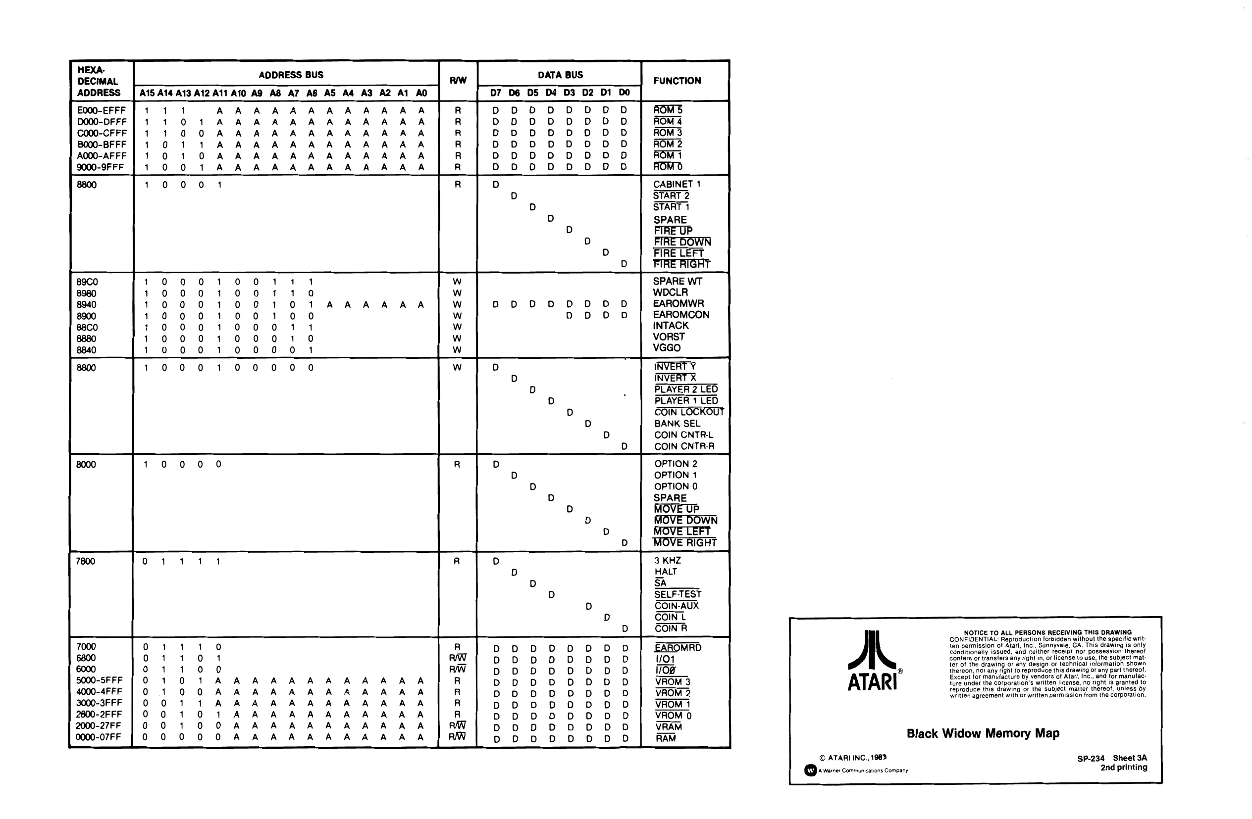
DECIMAL ADDRESS BUS
ADDRESS | A15 A14.A13 A12A11 A10 AQ AB A7 AG AS A4 A3 A2 Al AO E000-EFFF D000-DFFF C000-CFFF B000-BFFF A000-AFFF 9000-9F FF DATA BUS FUNCTION
D7 D6 D5 D4 D3 D2 D1 DO
CABINET 1 START 2 START 1 SPARE FIRE UP
FIRE DOWN FIRE RIGHT
FIRE LEFT
SPARE WT WDCLR EAROMWR EAROMCON INTACK VORST VGGO
INVERT Y
INVERT X PLAYER 2 LED PLAYER 1 LED COIN LOCKOUT BANK SEL COIN CNTR-L COIN CNTR-R
OPTION 2 OPTION 1 OPTION 0 SPARE efoccc0c0n0 eloccc0an0 eloccon00 °
SELF-TEST COIN-AUX COIN L COIN R NOTICE TO ALL PERSONS RECEIVING THIS DRAWING CONFIDENTIAL: Reproduction forbidden without the specific writ: ten permission of Atari, Inc., Sunnyvale, CA. This drawing is only conditionally issued, and neither receipt nor possession thereof confers or transfers any right in, or license to use, the subject matter of the drawing or any design or technical information shown
® thereon, nor any right to reproduce this drawing or any part thereof,
Except ior manufacture by vendors of Atari, Inc., and for manufacture under the Corporation's written license, no right is granted to reproduce this drawing or the subject matter thereof, unless by written agreement with or written permission from the corporation, R R R R R R
w w w w w w w
R RW RW R R R R RW RW escccoc00 o0000cg000 go0000000 ou0000000 ogo00000000 o00000000 o00000000 ogo00000000 vov000000]0
Black Widow Memory Map
© ATARI INC., 1983 SP-234 Sheet 3A Qt warre: commanzations Comoany 2nd printing
Descriptions of Black Widow Printed Circuit Board Names
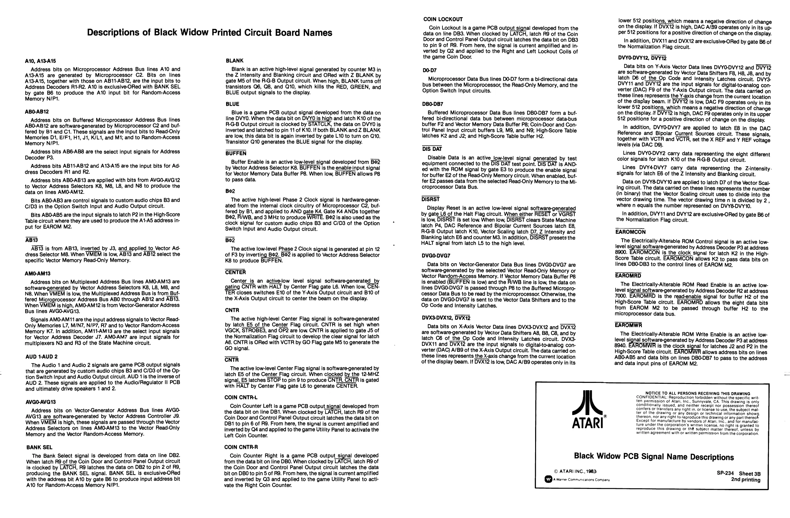
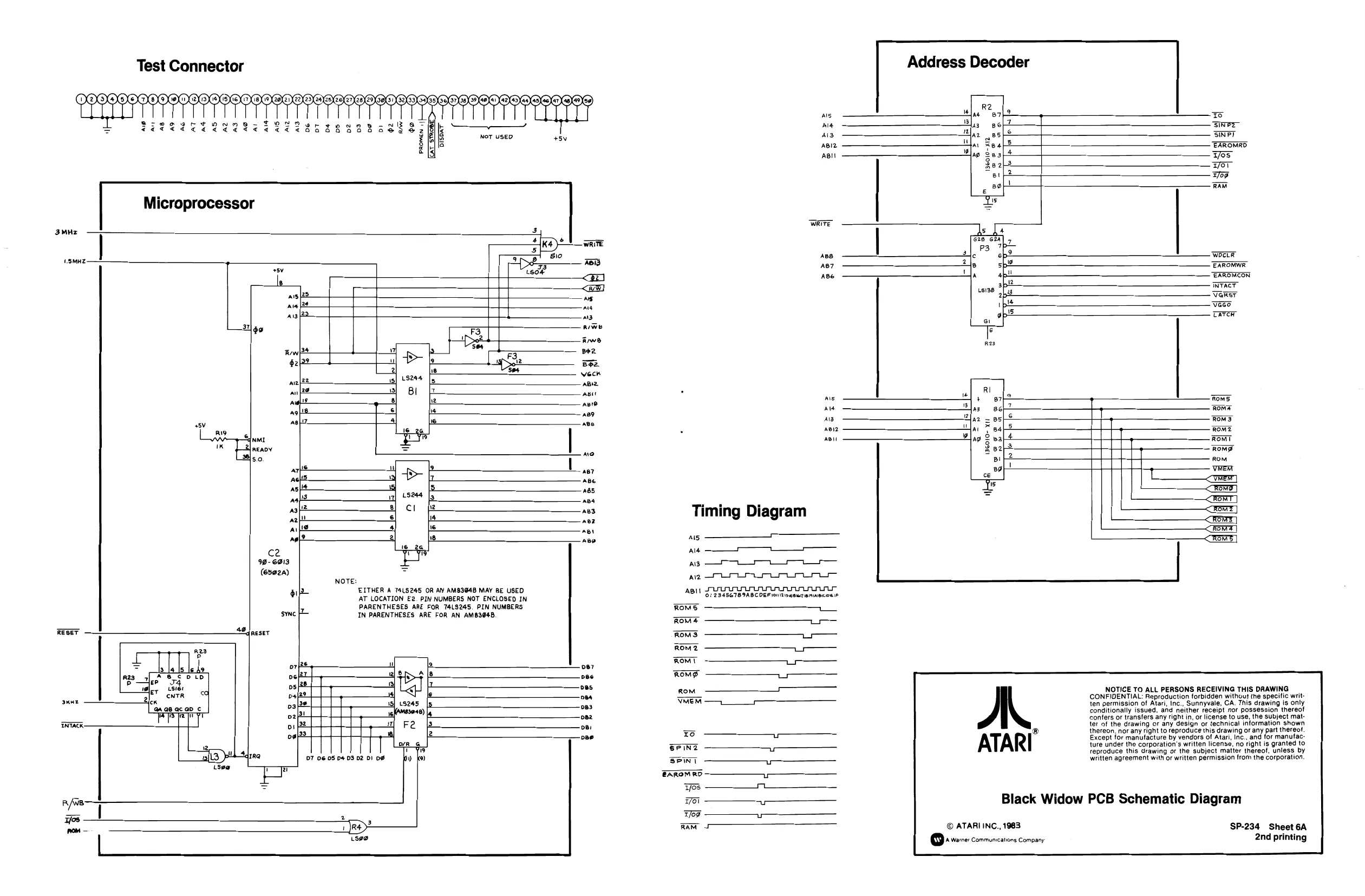
A10, A13-A15 Address bits on Microprocessor Address Bus lines A10 and A13-A15 are generated by Microprocessor C2. Bits on lines A13-A15, together with those on AB11-AB12, are the input bits to Address Decoders R1-R2. A10 is exclusive-ORed with BANK SEL by gate B6 to produce the A10 input bit for Random-Access Memory N/P1.
ABO-AB12 Address bits on Buffered Microprocessor Address Bus lines ABO-AB12 are software-generated by Microprocessor C2 and buffered by B1 and C1. These signals are the input bits to Read-Only Memories D1, E/F1, H1, J1, K/L1, and M1; and to Random-Access Memory N/P1. Address bits AB6-AB8 are the select input signals for Address Decoder P3. Address bits AB11-AB12 anc A13-A15 are the input bits for Address Decoders R1 and R2. Address bits ABO-AB13 are applied with bits from AVGO-AVG12 to Vector Address Selectors K8, M8, L8, and N8 to produce the data on lines AMO-AM12. Bits ABO-AB3 are control signals to custom audio chips B3 and C/D3 in the Option Switch Input and Audio Output circuit. Bits ABO-ABS5 are the input signals to latch P2 in the High-Score Table circuit where they are used to produce the A1-A5 address input for EAROM M2.
ABI3 ABTS is from AB13, inverted by J3, and applied to Vector Address Selector M8. When VMEM is low, AB13 and AB12 select the ‘specific Vector Memory Read-Only Memory.
AMO-AM13 Address bits on Multiplexed Address Bus lines AMO-AM13 are software-generated by Vector Address Selectors K8, L8, M8, and 8, When VMEM is low, the Multiplexed Address Bus is from Buffered Microprocessor Address Bus ABO through AB12 and AB13. When VMEN is high, AMO-AM12 is from Vector-Generator Address Bus lines AVGO-AVG13. Signals AMO-AM11 are the input address signals to Vector Read- Only Memories L7, M/N7, N/P7, R7 and to Vector Random-Access Memory K7. In addition, AM11-AM13 are the select input signals for Vector Address Decoder J7. AMO-AM7 are input signals for multiplexers N3 and R3 of the State Machine circuit.
AUD 1-AUD 2 The Audio 1 and Audio 2 signals are game PCB output signals that are generated by custom audio chips B3 and C/D3 of the Option Switch Input and Audio Output circuit. AUD 1 is the inverse of AUD 2. These signals are applied to the Audio/Reguiator Il PCB and ultimately drive speakers 1 and 2.
AVGO-AVG13 Address bits on Vector-Generator Address Bus lines AVGO- AVG13 are software-generated by Vector Address Controller J9. When VMEN is high, these signals are passed through the Vector Address Selectors on lines AMO-AM13 to the Vector Read-Only Memory and the Vector Random-Access Memory.
BANK SEL The Bank Select signal is developed from data on line DB2. When latch R9 of the Coin Door and Control Panel Output circuit is clocked by LATCH, R9 latches the data on DB2 to pin 2 of R9, producing the BANK SEL signal. BANK SEL is exclusive-ORed with the address bit A10 by gate B6 to produce input address bit A10 for Random-Access Memory N/P1. BLANK Blank is an active high-level signal generated by counter M3 in the Z Intensity and Blanking circuit and ORed with Z BLANK by gate M5 of the R-G-B Output circuit. When high, BLANK turns off transistors Q6, Q8, and Q10, which kills the RED, GREEN, and BLUE output signals to the display.
BLUE Blue is a game PCB output signal developed from the data on line DVYO. When the data bit on DVY0 Is high and latch K10 of the R-G-B Output circuit is clocked by STATCLK, the data on DVYO is inverted and latched to pin 11 of K10. If both BLANK and Z BLANK are low, this data bit is again inverted by gate L10 to turn on Q10. Transistor Q10 generates the BLUE signal for the display.
BUFFEN Buffer Enable is an active low-level signal developed from B&2 by Vector Address Selector K8. BUFFEN is the enable input signal for Vector Memory Data Buffer P8. When low, BUFFEN allows P8 to pass data.
Bo2 The active high-level Phase 2 Clock signal is hardware-generated from the internal clock circuitry of Microprocessor C2, buffered by B1, and applied to AND gate K4. Gate K4 ANDs together Bo2, R/WB, and 3 MHz to produce WRITE. B¢2 is also used as the clock signal for custom audio chips B3 and C/D3 of the Option Switch Input and Audio Output circuit.
Bo2 The active low-level Phase 2 Clock signal is generated at pin 12 of F3 by inverting B¢2. B02 is applied to Vector Address Selector K8 to produce BUFFEN.
CENTER Center_is an active-low level signal software-generated_by gating CNTR with HALT by Center Flag gate L6. When low, CEN- TER closes switches E10 of the Y-Axis Output circuit and B10 of the X-Axis Output circuit to center the beam on the display.
CNTR The active high-level Center Flag signal is software-generated by latch E5 of the Center Flag circuit. CNTR is set high when VGCK, STROBES, and OP2 are low CNTR is applied to gate J5 of the Normalization Flag circuit to develop the clear signal for latch AG. CNTR is ORed with VCTR by GO Flag gate M5 to generate the GO signal.
CNTR The active low-level Center Flag signal is software-generated by latch E5 of the Center Flag circuit. When clocked by the 12-MHZ signal, E5 latches STOP to pin 9 to produce CNTR. CNTR is gated with HALT by Center Flag gate L6 to generate CENTER.
COIN CNTR-L Coin Counter Left is a game PCB output signal developed from the data bit on line DB1. When clocked by LATCH, latch R9 of the Coin Door and Control Panel Output circuit latches the data bit on DB1 to pin 6 of R9. From here, the signal is current amplified and inverted by Q4 and applied to the game Utility Panel to activate the Left Coin Counter.
COIN CNTR-R Coin Counter Right is a game PCB output_signal developed from the data bit on line DBO. When clocked by LATCH, latch R9 of the Coin Door and Control Panel Output circuit latches the data bit on DBO to pin 5 of R9. From here, the signal is current amplified and inverted by Q3 and applied to the game Utility Panel to activate the Right Coin Counter. COIN LOCKOUT Coin Lockout is a game PCB output signal developed from the data on line DB3. When clocked by LATCH, latch R9 of the Coin Door and Control Panel Output circuit latches the data bit on DB3 to pin 9 of R9. From here, the signal is current amplified and inverted by Q2 and applied to the Right and Left Lockout Coils of the game Coin Door.
DO-D7 Microprocessor Data Bus lines D0-D7 form a bi-directional data bus between the Microprocessor, the Read-Only Memory, and the Option Switch Input circuits.
DBO-DB7 Buffered Microprocessor Data Bus lines DBO-DB7 form a buffered bi-directional data bus between microprocessor data-bus buffer F2 and Vector Memory Data Buffer P8; Coin-Door and Control Panel Input circuit buffers L9, M9, and N9; High-Score Table latches K2 and J2; and High-Score Table buffer H2.
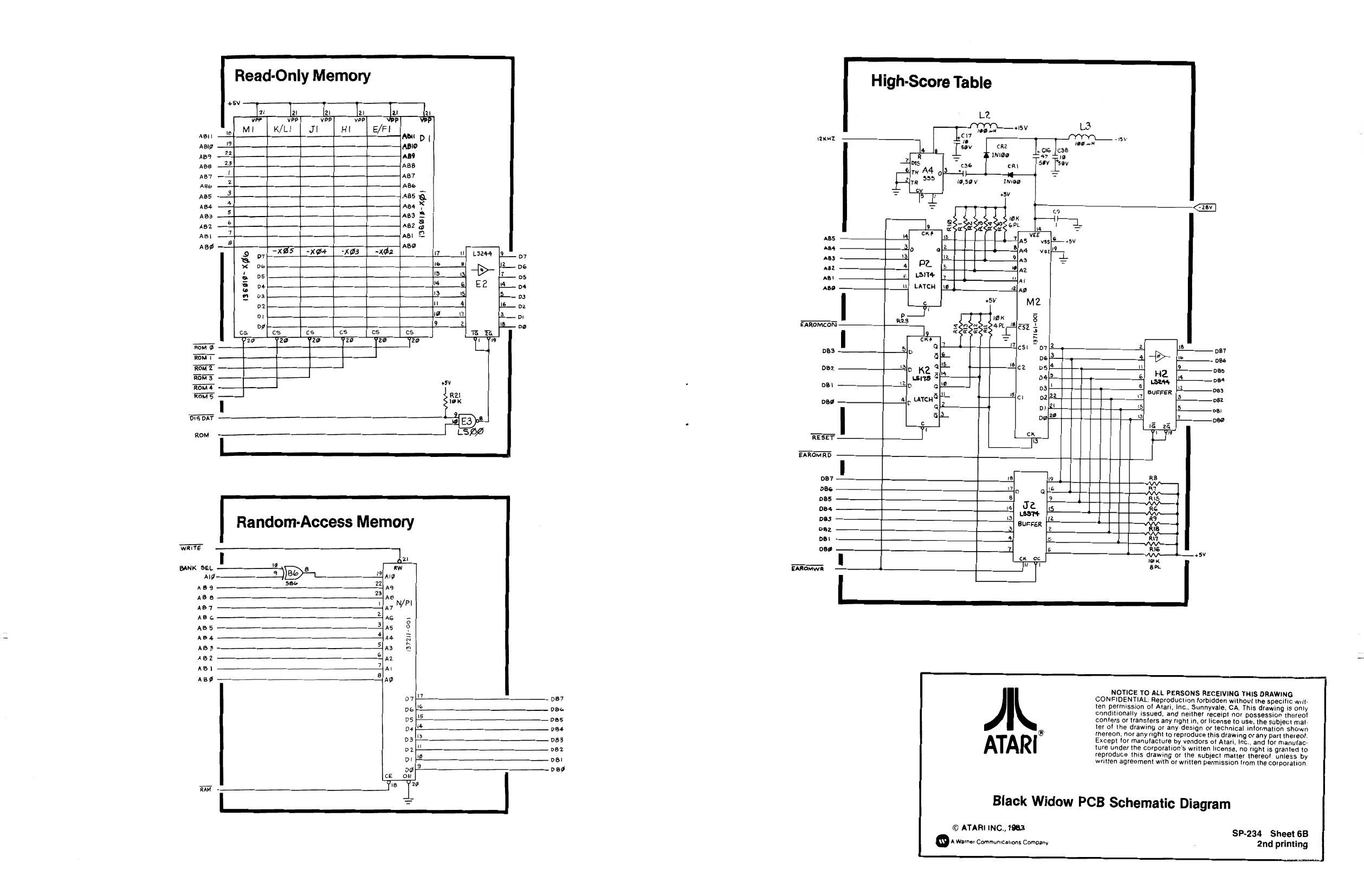
DIS DAT Disable Data is an active_low-level signal generated by test equipment connected to the DIS DAT test point. DIS DAT is ANDed with the ROM signal by gate E3 to produce the enable signal for buffer E2 of the Read-Only Memory circuit. When enabled, buffer E2 passes data from the selected Read-Only Memory to the Microprocessor Data Bus.
DISRST Display Reset is an active low-level signal software-generated by gate L6 of the Halt Flag circuit. When either RESET or VGRST is low, DISRST i8 set low When low, DISRST clears State Machine latch P4, DAC Reference and Bipolar Current Sources latch E8, R-G-B Output latch K10, Vector Scaling latch D7, Z Intensity and Blanking latch E6 and counter M3. In addition, DISRST presets the HALT signal from latch L5 to the high level.
DVGO-DVG7 Data bits on Vector-Generator Data Bus lines DVGO-DVG7 are software-generated by the selected Vector Read-Only Memory or Vector Random-Access Memory. If Vector Memory Data Buffer P8 is enabled (BUFFEN is low) and the R/WB line is low, the data on lines DVGO-DVG7 is passed through P8 to the Buffered Microprocessor Data Bus to be read by the microprocessor. Otherwise, the data on DVGO-DVG7 is sent to the Vector Data Shifters and to the Op Code and Intensity Latches.
DVX3-DVX12, DVX12 Data bits on X-Axis Vector Data lines DVX3-DVX12 and DVX12 are software-generated by Vector Data Shifters A8, B8, C8, and by latch C6 of the Op Code and Intensity Latches circuit. DVX3- DVX11 and DVX12 are the input signals to digital-to-analog converter (DAC) A/B9 of the X-Axis Output circuit. The data carried on these lines represents the X-axis change from the current location of the display beam. If DVX12 is low, DAC A/B9 operates only in its
AL ATARI
lower 512 positions, which means a negative direction of change
on the display. If DVX12 is high, DAC A/B9 operates only in its upper 512 positions for a positive direction of change on the display.
In addition, DVX11 and DVX12 are exclusive-ORed by gate B6 of
the Normalization Flag circuit.
DVYO-DVY12, DVY12 Data bits on Y-Axis Vector Data lines DVYO-DVY12 and DVYi2 are software-generated by Vector Data Shifters F8, H8, J8, and by latch D6 of the Op Code and Intensity Latches circuit. DVY- DVY11 and DVY12 are the input signals for digital-to-analog converter (DAC) F9 of the Y-Axis Output circuit. The data carried on these lines represents the Y-axis change from the current location of the display beam. If DVY72 is low, DAC F9 operates only in its
‘on the display. if DVY12 is high, DAC F9 operates only in its upper 512 positions for a positive direction of change on the display. In addition, DVYO-DVY7 are applied to latch E8 in the DAG Reference and Bipolar Current Sources circuit. These signals, together with VCTR and VCTR, set the X REF and Y REF voltage levels (via DAC D9), Lines DVYO-DVY2 carry data representing the eight different color signals for latch K10 of the R-G-B Output circuit. Lines DVY4-DVY7 carry data representing the Zintensity. signals for latch E6 of the Z Intensity and Blanking circuit. Data on DVY8-DVY10 are applied to latch D7 of the Vector Scaling circuit. The data carried on these lines represents the number (in binary) that the Vector Scaling circuit uses to divide into the
vector drawing time. The vector drawing time n is divided by 2,
where n equals the number represented on DVY8-DVY10. In addition, DVY11 and DVY12 are exclusive-ORed by gate B6 of the Normalization Flag circuit.
EAROMCON The Electrically-Alterable ROM Control signal is an active lowlevel signal software-generated by Address Decoder P3 at address 8900. EAROMCON is the clock signal for latch K2 in the High- Score Table circuit. EAROMCON allows K2 to pass data bits on lines DBO-DB3 to the control lines of EAROM M2.
EAROMRD The Electrically-Alterable ROM Read Enable is an active lowlevel signal software-generated by Address Decoder R2 at address 7000. EAROMRD is the read-enable signal for buffer H2 of the High-Score Table circuit. EAROMRD allows the eight data bits from EAROM M2 to be passed through buffer H2 to the microprocessor data bus.
EAROMWR The Electrically-Alterable ROM Write Enable is an active lowlevel signal software-generated by Address Decoder P3 at address
8940. is the clock signal for latches J2 and P2 in the
High-Score Table circuit. AROMA allows address bits on lines ‘ABO-AB5 and data bits on lines DBO-DB7 to pass to the address and data input pins of EAROM M2.
NOTICE TO ALL PERSONS RECEIVING THIS DRAWING CONFIDENTIAL: Reproduction forbidden without the specie wit ten permission of Atan, Inc. Sunnyvale, CA‘this orawing s Only Conditionally ssued, and neither receIpt nor possession thereot Confers or transfers any right nor license fo se, the subject matter of the drawing or any Gesign or technical information show thereon, nor any right to veproduce this drawing or any pat thereo Except for manufacture by vendors of Aten, Ine. and for manufac ture under the corporation's written license, no ight is granted fo reproduce this drawing or the subject matter thereot, unless by twhtten agreement with or written permission rom ine Corporation
Black Widow PCB Signal Name Descriptions
© ATARI INC., 1983 SP-234 Sheet 3B
Black Widow PCB Signal Name Descriptions, cont.
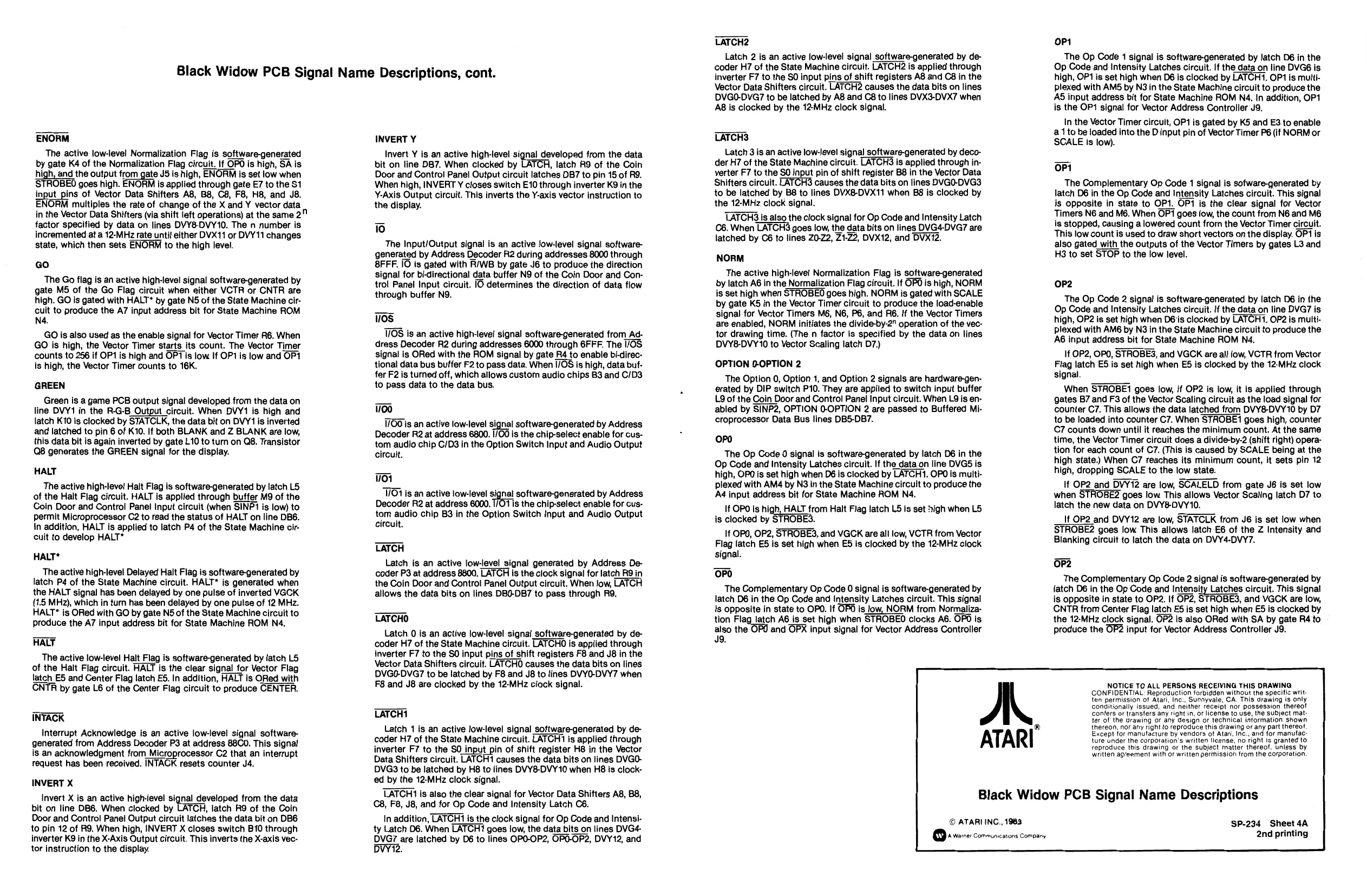
ENORM The active low-level Normalization Flag is software-generated by gate K4 of the Normalization Flag circuit. If OPO is high, SA is high, and the output from gate J5 is high, ENORM is set low when
STROBED goes high. ENORM is applied through gate E7 to the S1
input_pins of Vector Data Shifters A8, B8, C8, F8, H8, and J8. ENORM multiples the rate of change of the X and Y vector data in the Vector Data Shifters (via shift left operations) at the same 2" factor specified by data on lines DVY8-DVY10. The n number is incremented at a 12-MHz rate unti! either DVX11 or DVY11 changes state, which then sets ENORM to the high level.
Go The Go flag is an active high-level signal software-generated by gate M5 of the Go Flag circuit when either VCTR or CNTR are high. GO is gated with HALT* by gate N5 of the State Machine circuit to produce the A7 input address bit for State Machine ROM N4. GO is also used as the enable signal for Vector Timer R6. When GO is high, the Vector Timer starts its count. The Vector Timer
counts to 256 if OP1 is high and OPTis low If OP1 is low and OP1
is high, the Vector Timer counts to 16K.
GREEN Green is a game PCB output signal developed from the data on line DVY1 in the R-G-B Output circuit. When DVY1 is high and latch K10 is clocked by STATCLK, the data bit on DVY1 is inverted and latched to pin 6 of K10. If both BLANK and Z BLANK are low, this data bit is again inverted by gate L10 to turn on Q8. Transistor Q8 generates the GREEN signal for the display.
HALT The active high-leve! Halt Flag is software-generated by latch L5 of the Halt Flag circuit. HALT is applied through buffer M9 of the Coin Door and Control Panel Input circuit (when SINP1 is low) to permit Microprocessor C2 to read the status of HALT on line DB6. In addition, HALT is applied to latch P4 of the State Machine circuit to develop HALT*
HALT* The active high-level Delayed Halt Flag is software-generated by latch P4 of the State Machine circuit. HALT* is generated when the HALT signal has been delayed by one pulse of inverted VGCK (1.5 MHz), which in turn has been delayed by one pulse of 12 MHz. HALT* is ORed with GO by gate N5 of the State Machine circuit to Produce the A7 input address bit for State Machine ROM N4.
HALT The active low-level Halt Flag is software-generated by iatch L5 of the Halt Flag circuit. HALT is the clear signal for Vector Flag latch ES and Center Flag latch E5. In addition, HALT is ORed with CNTR by gate L6 of the Center Flag circuit to produce CENTER.
INTACK Interrupt Acknowledge is an active low-level signal softwaregenerated from Address Decoder P3 at address 88C0. This signal is an acknowledgment from Microprocessor C2 that an interrupt request has been received. INTACK resets counter J4.
INVERT X Invert X is an active high-level signal developed from the data bit on line DB6. When clocked by H, latch R9 of the Coin Door and Control Panel Output circuit latches the data bit on DB6 to pin 12 of R9. When high, INVERT X closes switch B10 through inverter K9 in the X-Axis Output circuit. This inverts the X-axis vector instruction to the display. INVERT Y Invert Y is an active high-level signal developed from the data bit on line DB7. When clocked by |, latch R9 of the Coin Door and Control Panel Output circuit latches DB7 to pin 15 of R9. When high, INVERT Y closes switch E10 through inverter K9 in the Y-Axis Output circuit. This inverts the Y-axis vector instruction to the display.
The Input/Output signal is an active low-level signal softwaregenerated by Address Decoder R2 during addresses 8000 through 8FFF. IO is gated with R/WB by gate J6 to produce the direction ‘signal for bi-directional data buffer N9 of the Coin Door and Control Panel Input circuit. IO determines the direction of data flow through buffer N9.
IOS is an active high-level signal software-generated from Address Decoder R2 during addresses 6000 through 6FFF. The I/OS signal is ORed with the ROM signal by gate Ré4 to enable bi-directional data bus buffer F2 to pass data. When 1/08 is high, data buffer F2 is turned off, which allows custom audio chips 83 and C/D3 to pass data to the data bus.
\/00 is an active low-level signal software-generated by Address Decoder R2 at address 6800. 1/00 is the chip-select enable for custom audio chip C/D3 in the Option Switch Input and Audio Output circult.
(/01 is an active low-level signal software-generated by Address Decoder R2 at address 6000. 1/O1is the chip-select enable for custom audio chip B3 in the Option Switch input and Audio Output circuit.
LATCH Latch is an active low-level signal generated by Address Decoder P3 at address 8800. LATCH is the clock signal for latch R9 in the Coin Door and Control Panel Output circuit. When low, LATCH allows the data bits on lines DBO-DB7 to pass through R9.
LATCHO Latch 0 is an active low-level signai_software-generated by decoder H7 of the State Machine circuit. LATCHO is appiied through inverter F7 to the SO input pins of shift registers F8 and J8 in the Vector Data Shifters circuit. LATCHO causes the data bits on lines DVG0-DVG7 to be latched by F8 and J8 to tines DVY0-DVY7 when F8 and J8 are clocked by the 12-MHz ciock signal.
LATCHi Latch 1 is an active low-level signal software-generated by decoder H7 of the State Machine circuit. LATCH1 is applied through inverter F7 to the SO input pin of shift register H8 in the Vector Data Shifters circuit. LATCH causes the data bits on lines DVGO- DVG3 to be latched by H8 to lines DVY8-DVY 10 when H8 is clocked by the 12-MHz clock signal. LATCH1 is also the clear signal for Vector Data Shifters A8, B8, C8, F8, J8, and for Op Code and Intensity Latch C6. In addition, LATCH is the clock signal for Op Code and Intensity Latch 06. When LATCH? goes low, the data bits on lines DVG4- DVG7 are latched by D6 to lines OPO-OP2, OPO-OP2, DVY12, and DVY72. LATCH2 Latch 2 is an active low-level signal _software-generated by decoder H7 of the State Machine circuit. LATCH2 is applied through inverter F7 to the SO input pins of shift registers A8 and C8 in the Vector Data Shifters circuit. LATCH2 causes the data bits on lines DVG0-DVG7 to be latched by A8 and C8 to lines DVX3-DVX7 when A8 is clocked by the 12-MHz clock signal.
LATCH3 Latch 3 is an active low-level signal software-generated by decoder H7 of the State Machine circuit. LATCHG is applied through inverter F7 to the SO input pin of shift register B8 in the Vector Data
Shifters circuit. LAI causes the data bits on lines DVGO-DVG3
to be latched by B8 to lines DVX8-DVX11 when B8 is clocked by the 12-MHz clock signal. LATCH is also the clock signal for Op Code and Intensity Latch C6. When LATCH3 goes low, the data bits on lines DVG4-DVG7 are latched by C6 to lines Z0-22, 21-22, DVX12, and DVX72.
NORM The active high-level Normalization Flag is software-generated by latch A6 in the Normalization Flag circuit. If OPO is high, NORM is set high when STROBEO goes high. NORM is gated with SCALE by gate K5 in the Vector Timer circuit to produce the load-enable signal-for Vector Timers M6, N6, P6, and R6. If the Vector Timers are enabled, NORM initiates the divide-by-2" operation of the vector drawing time. (The n factor is specified by the data on lines DVY8-DVY10 to Vector Scaling latch D7.)
OPTION G-OPTION 2 The Option 0, Option 1, and Option 2 signals are hardware-generated by DIP switch P10. They are applied to switch input buffer L9 of the Coin Door and Control Panel Input circuit. When L9 is enabled by SINP2, OPTION 0-OPTION 2 are passed to Buffered Microprocessor Data Bus lines DB5-DB7.
OPO The Op Code 0 signal is software-generated by latch D6 in the Op Code and Intensity Latches circuit. If the data on line DVGS5 is high, OP9 is set high when D6 is clocked by LATCH1. OPO is multiplexed with AM4 by N@ in the State Machine circuit to produce the A4 input address bit for State Machine ROM N4. If OPO is high, HALT from Halt Flag latch L5 Is set nigh when L5 is clocked by STROBES. \f OPO, OP2, STROBES, and VGCK are all low, VCTR from Vector Flag latch E5 is set high when E65 is clocked by the 12-MHz clock signal.
‘OPO The Complementary Op Code 0 signal is software-generated by latch D6 in the Op Code and Intensity Latches circuit. This signal ts opposite in state to OPO. If OPO is low, NORM from Normalization Flag_latch A6 is set high when STROBEO clocks A6. OPO is also the OPO and OPX input signal for Vector Address Controller J9.
A, ATARI ‘OP1 The Op Code 1 signal is software-generated by /atch D6 in the Op Code and Intensity Latches circuit. If the data on line DVG6 is high, OP1 is set high when D6 is clocked by LATCH1, OP1 is muttiplexed with AM5 by N3 in the State Machine circuit to produce the AS input address bit for State Machine ROM N4. In addition, OP1 is the OP1 signal for Vector Address Controller J9, In the Vector Timer circuit, OP1 is gated by K5 and E3 to enable a1 to be loaded into the D input pin of Vector Timer P6 (if NORM or SCALE is low).
OPi The Complementary Op Code 1 signal is sofware-generated by latch D6 in the Op Code and Intensity Latches circuit. This signal is opposite in state to OP1. OP1 is the clear signal for Vector Timers N6 and M6. When OP1 goes fow, the count from N6 and M6 is stopped, causing a lowered count from the Vector Timer circuit. This low count is used to draw short vectors on the display. OP1 is also gated with the outputs of the Vector Timers by gates L3 and H3 to set STOP to the low level.
OPp2 The Op Code 2 signa! is software-generated by latch D6 in the Op Code and Intensity Latches circuit. If the data on line DVG7 is high, OP2 is set high when D6'is clocked by LATCH1, OP2 is multiplexed with AM6 by NG in the State Machine circuit to produce the A6 input address bit for State Machine ROM N4. If OP2, OPO, STROBES, and VGCK are all iow, VCTR from Vector Flag latch ES is set high when E65 is clocked by the 12-MHz clock signal. When STROBE1 goes low, if OP2 is low, it is applied through gates B7 and F3 of the Vector Scaling circuit as the load signal for counter C7. This allows the data latched from DVY8-DVY10 by D7 to be loaded into counter C7. When STROBE1 goes high, counter C7 counts down until it reaches the minimum count. At the same time, the Vector Timer circuit does a divide-by-2 (shift right) operation for each count of C7. (This is caused by SCALE being at the high state.) When C7 reaches its minimum count, it sets pin 12 high, dropping SCALE to the low state. \f OP2 and DVY12 are low, SCALELD from gate Jé6 is set low
when STROBEZ2 goes low This allows Vector Scaling latch D7 to
latch the new data on DVY8-DVY10. If OP2 and DVY12 are low, STATCLK from J6 is set low when STROBE2 goes low This allows latch E6 of the Z Intensity and Blanking circuit to latch the data on DVY4-DVY7.
oF2 The Complementary Op Code 2 signal is software-generated by latch D6 in the Op Code and Intensity Latches circuit. This signal is opposite in state to OP2. If OPZ, STROBES, and VGCK are low, CNTR from Center Flag latch £5 is set high when E5 is clocked by the 12-MHz clock signal. OP2 is also ORed with SA by gate Ré4 to produce the OP2 input for Vector Address Controller J9.
NOTICE TO ALL PERSONS RECEIVING THIS DRAWING CONFIDENTIAL: Reproduction forbidden without the specific writ. ten permission of Atari, Inc., Sunnyvale, CA. This drawing is only conditionally issued, and neither receipt nor possession thereot confers or transfers any right in, or license to use, the subject matter of the drawing or any design or technical injormation shown
thereon, nor any right to reproduce this drawing or any part thereot
Except for manutacture by vendors of Atari, Inc., and for manufac ture Under the corporation's written license, no right is granted to reproduce this drawing or the subject matter thereof. unless by written agreement with or written permission from the corporation.
Black Widow PCB Signal Name Descriptions
© ATARIINC., 1983 ‘SP-234 Sheet 4A
Black Widow PCB Signal Name Descriptions, cont.
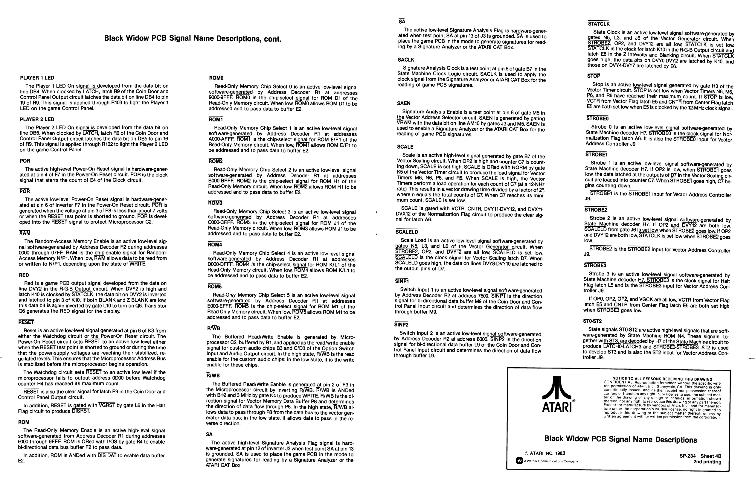
PLAYER 1 LED The Player 1 LED On signal is developed from the data bit on line DB4. When clocked by LATCH, latch R9 of the Coin Door and Control Panel Output circuit latches the data bit on line DB4 to pin 19 of R9. This signal is applied through R103 to light the Player 1 LED on the game Control Panel.
PLAYER 2 LED The Player 2 LED On signai is developed from the data bit on line DB5. When clocked by LATCH, latch R9 of the Coin Door and Control Panel Output circuit latches the data bit on DBS to pin 16
of R9. This signal is applied through R102 to light the Player 2 LED
on the game Control Panel.
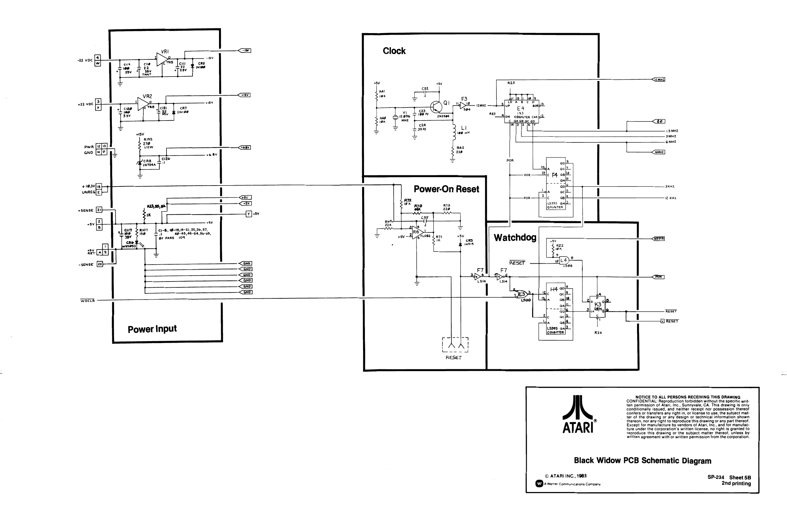
POR The active high-level Power-On Reset signal is hardware-generated at pin 4 of F7 in the Power-On Reset circuit. POR is the clock signal that starts the count of E4 of the Clock circuit.
POR The active low-level Power-On Reset signal is hardware-generated at pin 6 of inverter F7 in the Power-On Reset circuit. POR is generated when the voltage at pin 3 of R8 is less than about 7 volts or when the RESET test point is shorted to ground. POR is developed into the RESET signal to protect Microprocessor C2.
RAM The Random-Access Memory Enable is an active low-level signal software-generated by Address Decoder R2 during addresses 0000 through 07FF. RAM is the chip-enable signal for Random- Access Memory N/P1. When low, RAM allows data to be read from or written to N/P1, depending upon the state of WRITE.
Red is a game PCB output signal developed from the data on line DVY2 in the R-G-B Output circuit. When DVY2 is high and latch K10 is clocked by STATCLK, the data bit on DVY2 is inverted and latched to pin 3 of K10. If both BLANK and Z BLANK are low, this data bit is again inverted by gate L10 to turn on Q6. Transistor Q6 generates the RED signal for the display.
RESET Reset is an active low-level signal generated at pin 6 of K3 from either the Watchdog circuit or the Power-On Reset circuit. The Power-On Reset circuit sets RESET to an active low level either when the RESET test point is shorted to ground or during the time that the power-supply voltages are reaching their stabilized, regu-lated levels. This ensures that the Microprocessor Address Bus is stabilized before the microprocessor begins operation. The Watchdog circuit sets RESET to an active low level if the microprocessor fails to output address 0D00 before Watchdog counter H4 has reached its maximum count. RESET is also the clear signal for latch R9 in the Coin Door and Control Panel Output circuit.
In addition, RESET is gates with VGRST by gate L6 in the Halt
Flag circuit to produce RST.
ROM The Read-Only Memory Enable is an active high-level signal software-generated from Address Decoder R1 during addresses 9000 through 9FFF. ROM is ORed with I/OS by gate Ré to enable bi-directional data bus buffer F2 to pass data. In addition, ROM is ANDed with DIS DAT to enable data buffer ROMO Read-Only Memory Chip Select 0 is an active low-level signal
| software-generated | by | Address | Decoder | R1 | at | addresses |
9000-9FFF. ROMO is the chip-select signal for ROM D1 of the Read-Only Memory circuit. When low, ROMO allows ROM D1 to be addressed and to pass data to buffer E2.
ROM1 Read-Only Memory Chip Select 1 is an active low-level signal
| software-generated | by | Address | Decoder | R1 | at | addresses |
A000-AFFF. ROM1 is the chip-select signal for ROM E/F1 of the Read-Only Memory circuit. When low, ROM1 allows ROM E/F1 to be addressed and to pass data to buffer E2.
ROM2 Read-Only Memory Chip Select 2 is an active low-level signal
| software-generated | by | Address | Decoder | R1 | at | addresses |
B000-BFFF. RON2 is the chip-select signal for ROM H1 of the Read-Only Memory circuit. When low, allows ROM H1 to be addressed and to pass data to buffer E2.
ROM3 Read-Only Memory Chip Select 3 is an active low-level signal
| software-generated | by | Address | Decoder | R1 | at | addresses |
CO00-CFFF. ROMS is the chip-select_signal for ROM J1 of the Read-Only Memory circuit. When low, 13 allows ROM J1 to be addressed and to pass data to buffer E2.
ROM4 Read-Only Memory Chip Select 4 is an active low-level signal
| software-generated | by | Address | Decoder | R1 | at | addresses |
D000-DFFF. ROM4 is the chip-select signal for ROM K/L1 of the Read-Only Memory circuit. When low, 4 allows ROM K/L1 to be addressed and to pass data to buffer E2.
ROMS Read-Only Memory Chip Select 5 is an active low-level signal
| software-generated | by | Address | Decoder | R1 | at | addresses |
E000-EFFF. ROMS is the chip-select_signal for ROM M1 of the Read-Only Memory circuit. When low, ROMS allows ROM M1 to be addressed and to pass data to buffer E2.
RWB The Buffered Read/Write Enable is generated by Microprocessor C2, buffered by B1, and applied as the read/write enable signal for custom audio chips B3 and C/D3 of the Option Switch Input and Audio Output circuit. In the high state, R/WB is the read enable for the custom audio chips; in the low state, it is the write enable for these chips.
RWB The Buffered Read/Write Eanble is generated at pin 2 of F3 in the Microprocessor circuit by inverting R/WB. R/WB is ANDed with B¢2 and 3 MHz by gate K4 to produce WRITE. R/WB is the direction signal for Vector Memory Data Buffer P8 and determines the direction of data flow through P8. In the high state, R/WB allows data to pass through P8 from the data bus to the vector generator data bus; in the low state, it allows data to pass in the reverse direction.
SA The active high-level Signature Analysis Flag signal is hardware-generated at pin 12 of inverter J3 when test point SA at pin 13 is grounded. SA is used to place the game PCB in the mode to generate signatures for reading by a Signature Analyzer or the ATARI CAT Box. SA The active low-level Signature Analysis Flag is hardware-generated when test point SA at pin 13 of J3 is grounded. SA is used to place the game PCB in the mode to generate signatures for reading by a Signature Analyzer or the ATARI CAT Box.
SACLK Signature Analysis Clock is a test point at pin 8 of gate B7 in the State Machine Clock Logic circuit. SACLK is used to apply the clock signal from the Signature Analyzer or ATARI CAT Box for the reading of game PCB signatures.
SAEN Signature Analysis Enable is a test point at pin 8 of gate M5 in the Vector Address Selector circuit. SAEN is generated by gating VRAM with the data bit on line AM10 by gates J3 and M5. SAEN is used to enable a Signature Analyzer or the ATARI CAT Box for the reading of game PCB signatures.
SCALE Scale is an active high-level signal generated by gate B7 of the Vector Scaling circuit. When OP2 is high and counter G7 is counting down, SCALE is set high. SCALE is ORed with NORM by gate KS of the Vector Timer circuit to produce the load signal tor Vector Timers M6, N6, P6, and R6. When SCALE is high, the Vector Timers perform a load operation for each count of C7 (at a 12-NHz rate). This results in a vector drawing time divided by a factor of 2", where n equals the total counts of C7. When C7 reaches its minimum count, SCALE is set low. SCALE is gated with VCTR, CNTR, DVY11-DVY12, and DVX11- DVX12 of the Normalization Flag circuit to produce the clear signal for latch A6.
SCALELD ‘Scale Load is an active low-level signal software-generated by gates_N5, L3, and L6 of the Vector Generator circuit. When STROBE2, OP2, and DVY12 are all low, SCALELD is set low SCALELD is the clock signal for Vector Scaling latch D7. When SCALELD goes high, the data on lines DVY8-DVY10 are latched to the output pins of D7.
‘SINP1 Switch Input 1 is an active low-level signal software-generated by Address Decoder R2 at address 7800. SINP1 is the direction signal for bi-directional data buffer M9 of the Coin Door and Control Panel Input circuit and determines the direction of data flow through buffer M9.
‘SINP2 Switch Input 2 is an active low-level signal software-generated by Address Decoder R2 at address 8000. SINP2 is the direction signal for bi-directional data buffer L9 of the Coin Door and Control Panel Input circuit and determines the direction of data flow through buffer L9.
A
ATARI
© ATARI INC., 1983, STATCLK State Clock is an active low-level signal software-generated by jates_N5, L3, and J6 of the Vector Generator circuit. When » OP2, and DVY12 are all low, STATCLK is set low STATCLK is the clock for latch K10 in the R-G-B Output circuit and latch E6 in the Z Intensity and Blanking circuit. When STATCLK goes high, the data bits on DVYO-DVY2 are latched by K10, and those on DVY4-DVY7 are latched by E6.
STOP Stop is an active low-level signal generated by gate H3 of the
Vector Timer circuit. STOP is set low when Vector Timers N6, M6, ES are both set low when ES is clocked by the 12-MHz clock signal
P6,and R6 have reached their maximum count. If STOP is low, VCTR from Vector Flag latch E5 and CNTR from Center Flag latch ES are both set low when ES is clocked by the 12-MHz clock signal.
STROBEO Strobe 0 is an active low-level signal software-generated by State Machine decoder H7. STROBEO is the clock signal for Nor- Mmalization Flag latch A6. It is also the STROBEO input for Vector Address Controller J9.
STROBE1 Strobe 1 is an active low-level signal software-generated by State Machine decoder H7. If OP2 is low, when STROBE1 goes low, the data latched at the outputs of D7 in the Vector Scaling circuit are loaded into counter C7. When STROBE? goes high, C7 begins counting down. STROBE1 is the STROBE1 input for Vector Address Controller J9.
STROBE2 Strobe 2 is an active low-level signal software-generated by State Machine decoder H7. If OP2 and DVY72 are both low, SCALELD from gate Jé6 is set low when STROBE2 goes low If OP2 and DVY 12 are both low, STATCLK is set low when STROBE2 goes low. STROBE2 is the STROBE2 input for Vector Address Controller J9.
STROBE3 Strobe 3 is an active low-level_signal software-generated by State Machine decoder H7. STROBES is the clock signal for Halt Flag latch L5 and is the STROBES input for Vector Address Controller J9. If OPO, OP2, OP2, and VGCK are all low, VCTR from Vector Flag latch E5_and CNTR from Center Flag latch E5 are both set high when STROBE3 goes low
STO-ST2 State signals STO-ST2 are active high-level signals that are software-generated by State Machine ROM N4. These signals, together with ST3, are decoded by H7 of the State Machine circuit to Produce LATCHO-LATCH3 and STROBEO-STROBES. ST2 is used to develop ST3 and is also the ST2 input for Vector Address Controller J9.
NOTICE TO ALL PERSONS RECEIVING THIS DRAWING CONFIDENTIAL: Reproduction forbidden without the specific written permission of Atari, inc.. Sunnyvale, CA. This drawing is only Conditionally issued, and neither receipt nor possession thereof confers or transfers any right in, or license to use, the subject mat: ter of the drawing or any design or technical information shown thereon, nor any right to reproduce this drawing or any part thereof. Except for manufacture by vendors of Atari, Inc., and for manufac. ture under the corporation's written license, no right is granted to feproduce this drawing or the subject matter thereof, unless by written agreement with or written permission from the corporation
Black Widow PCB Signal Name Descriptions
SP-234 Sheet 4B
Black Widow PCB Signal Name Descriptions, cont.
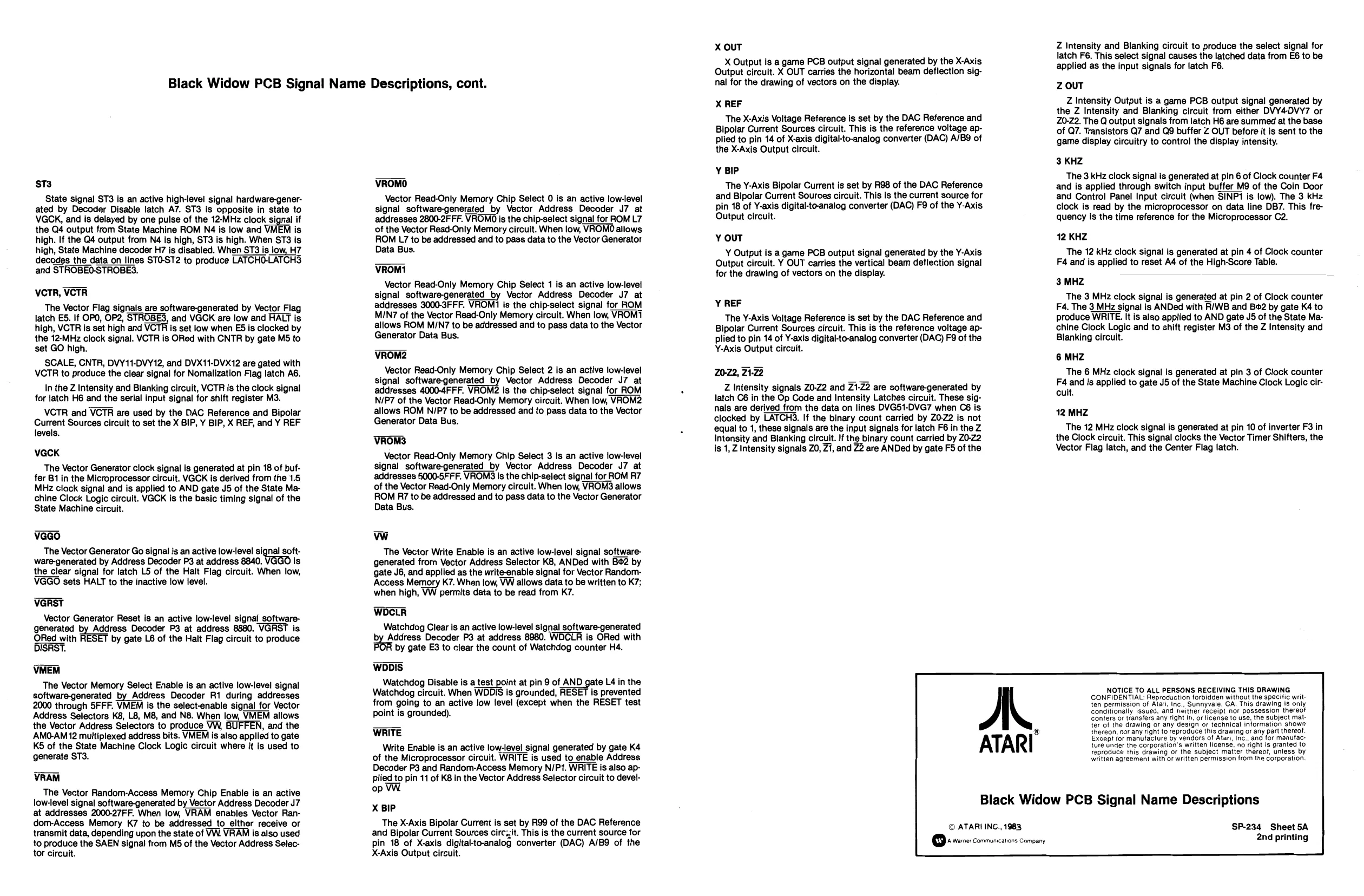
ST3 State signal ST3 is an active high-level signal hardware-generated by Decoder Disable latch A7. ST3 is opposite in state to VGCK, and is delayed by one pulse of the 12-MHz clock signal if the Q4 output from State Machine ROM N4 is low and VMEM is high. If the Q4 output from N4 is high, ST3 is high. When ST3 is high, State Machine decoder H7 is disabled. When ST3 is low, H7 decodes the data on lines STO-ST2 to produce LATCHO-LATCH3 and STROBEO-STROBES.
VCTR, VCTR The Vector Flag signals are software-generated by Vector Flag latch E5. If OPO, OP2, STROBES, and VGCK are low and HALT is high, VCTR is set high and VCTR is set low when E5 is clocked by the 12-MHz clock signal. VCTR is ORed with CNTR by gate M5 to set GO high. SCALE, CNTR, DVY11-DVY12, and DVX11-DVX12 are gated with VCTR to produce the clear signal for Nomalization Flag latch A6. In the Z Intensity and Blanking circuit, VCTR is the clock signal for latch H6 and the serial input signal for shift register M3. VCTR and VCTR are used by the DAC Reference and Bipolar Current Sources circuit to set the X BIP, Y BIP, X REF, and Y REF levels.
VGCK The Vector Generator clock signal is generated at pin 18 of buffer B1 in the Microprocessor circuit. VGCK is derived from the 1.5 MHz clock signal and is applied to AND gate J5 of the State Machine Clock Logic circuit. VGCK is the basic timing signal of the State Machine circuit.
VGGO The Vector Generator Go signal is an active low-level signal Software-generated by Address Decoder P3 at address 8840. is the clear signal for latch L5 of the Halt Flag circuit. When low, VGGO sets HALT to the inactive low level.
VGRST Vector Generator Reset is an active low-level signal software-
generated Ps Address Decoder P3 at address 8880. VGRST is
preawith RESET by gate L6 of the Halt Flag circuit to produce
VMEM The Vector Memory Select Enable is an active low-level signal software-generated by Address Decoder R1 during addresses 2000 through 5FFF. VMEM is the select-enable signal for Vector Address Selectors K8, L8, M8, and N8. When low, VMEM allows the Vector Address Selectors to produce VW, BUFFEN, and the AM0-AM12 multiplexed address bits. VMEM is also applied to gate K5 of the State Machine Clock Logic circuit where it is used to generate ST3.
VRAM The Vector Random-Access Memory Chip Enable is an active low-level signal software-generated by Vector Address Decoder J7 at addresses 2000-27FF. When low, VRAM enables Vector Random-Access Memory K7 to be addressed _to either receive or transmit data, depending upon the state of VW. VRAM is also used to produce the SAEN signal from M5 of the Vector Address Selector circuit. VROMO Vector Read-Only Memory Chip Select 0 is an active low-level signal software-generated by Vector Address Decoder J7 at addresses 2800-2FFF. VROMO is the chip-select signal for ROM L7 of the Vector Read-Only Memory circuit. When low, VROMO allows ROM L7 to be addressed and to pass data to the Vector Generator Data Bus.
VROM1 Vector Read-Only Memory Chip Select 1 is an active low-level signal software-generated_by Vector Address Decoder J7 at addresses 3000-3FFF. VROM1 is the chip-select signal for ROM MIN7 of the Vector Read-Only Memory circuit. When low, VROM1 allows ROM MI/N7 to be addressed and to pass data to the Vector Generator Data Bus.
VROM2 Vector Read-Only Memory Chip Select 2 is an active low-level signal software-generated by Vector Address Decoder J7 at addresses 4000-4FFF. VROM2 is the chip-select signal for ROM N/P7 of the Vector Read-Only Memory circuit. When low, VROM2 allows ROM N/P7 to be addressed and to pass data to the Vector Generator Data Bus.
VROM3 Vector Read-Only Memory Chip Select 3 is an active low-level signal software-generated_by Vector Address Decoder J7 at addresses 5000-5FFF. VROM3 is the chip-select signal for ROM R7 of the Vector Read-Only Memory circuit. When low, VROM3 allows ROM R7 to be addressed and to pass data to the Vector Generator Data Bus.
Ww The Vector Write Enable is an active low-level signal softwaregenerated from Vector Address Selector K8, ANDed with Bo2 by gate J6, and applied as the write-enable signal for Vector Random- Access Memory K7. When low, VW allows data to be written to K7; when high, VW permits data to be read from K7.
WOCLR Watchdog Clear is an active low-level signal software-generated by Address Decoder P3 at address 8980. WOCLR is ORed with by gate E3 to clear the count of Watchdog counter H4.
WDDIS
Watchdog Disable is a test point at pin 9 of AND pate L4 inthe
Watchdog circuit. When WDDIS is grounded, RE is prevented from going to an active Jow level (except when the RESET test point is grounded).
WRITE Write Enable is an active low-level signal generated by gate K4 of the Microprocessor circuit. WRITE is used to enable Address Decoder P3 and Random-Access Memory N/Pt. WRITE is also applied to pin 11 of K8 in the Vector Address Selector circuit to develop WW.
X BIP The X-Axis Bipolar Current is set by R99 of the DAC Reference and Bipolar Current Sources cir This is the current source for pin 18 of X-axis digital-to-analog converter (DAC) A/B9 of the X-Axis Output circuit. X OUT X Output is a game PCB output signal generated by the X-Axis Output circuit. X OUT carries the horizontal beam deflection signal for the drawing of vectors on the display.
X REF The X-Axis Voltage Reference is set by the DAC Reference and Bipolar Current Sources circuit. This is the reference voltage ap- Plied to pin 14 of X-axis digital-to-analog converter (DAC) A/B9 of the X-Axis Output circuit.
Y BIP The Y-Axis Bipolar Current is set by R98 of the DAC Reference and Bipolar Current Sources circuit. This is the current source for pin 18 of Y-axis digital-to-analog converter (DAC) F9 of the Y-Axis Output circuit.
Y OUT Y Output is a game PCB output signal generated by the Y-Axis Output circuit. Y OUT carries the vertical beam deflection signal for the drawing of vectors on the display.
Y REF The Y-Axis Voltage Reference is set by the DAC Reference and Bipolar Current Sources circuit. This is the reference voltage applied to pin 14 of Y-axis digital-to-analog converter (DAC) F9 of the Y-Axis Output circuit.
20-22, 21-22 Z Intensity signals Z0-22 and Z1-Z2 are software-generated by latch C6 in the Op Code and Intensity Latches circuit. These signals are derived from the data on lines DVG51-DVG7 when C6 is clocked by LATCH3. If the binary count carried by Z0-Z2 is not equal to 1, these signals are the input signals for latch F6 in the Z Intensity and Blanking circuit. If the binary count carried by Z0-22 is 1, Z Intensity signals ZO, Z1, and 22 are ANDed by gate F5 of the
ATARI
Z Intensity and Blanking circuit to produce the select signal for latch F6. This select signal causes the latched data from E6 to be applied as the input signals for latch F6.
Z OUT Z Intensity Output is a game PCB output signal generated by the Z Intensity and Blanking circuit from either DVY4-DVY7 or Z0-Z2. The Q output signals from latch H6 are summed at the base of Q7. Transistors Q7 and Q9 buffer Z OUT before it is sent to the game display circuitry to control the display intensity.
3 KHZ The 3 kHz clock signal is generated at pin 6 of Clock counter F4 and is applied through switch input buffer M9 of the Coin Door and Control Panel Input circuit (when SINP1 is low). The 3 kHz clock is read by the microprocessor on data line DB7. This frequency is the time reference for the Microprocessor C2.
12 KHZ The 12 kHz clock signal is generated at pin 4 of Clock counter F4 and is applied to reset A4 of the High-Score Table.
3 MHZ The 3 MHz clock signal is generated at pin 2 of Clock counter F4. The 3 MHz signal is ANDed with R/WB and B¢2 by gate K4 to produce WRITE. It is also applied to AND gate J5 of the State Machine Clock Logic and to shift register M3 of the Z Intensity and Blanking circuit.
6 MHZ The 6 MHz clock signal is generated at pin 3 of Clock counter F4 and Is applied to gate J5 of the State Machine Clock Logic circuit.
12 MHZ The 12 MHz clock signal is generated at pin 10 of inverter F3 in the Clock circuit. This signal clocks the Vector Timer Shifters, the Vector Flag latch, and the Center Flag latch.
NOTICE TO ALL PERSONS RECEIVING THIS DRAWING
CONFIDENTIAL: Reproduction forbidden without the specitic writ: confers or transfers any right in, or license to use, the subject mat
ten permission of Atari, Inc., Sunnyvale, CA. This drawing is only conditionally issued, and neither receipt nor possession thereot confers or transfers any right in, or license to use, the subject matter of the drawing or any design or technical information shown thereon, nor any right to reproduce this drawing or any part thereof. Except for manufacture by vendors of Atari, Inc., and for manufac: ture under the corporation's written license. no right is granted to reproduce this drawing or the subject matter thereof, unless by written agreement with or written permission from the corporation.
Black Widow PCB Signal Name Descriptions
© ATARI ING., 1983, SP-234 Sheet 5A
This page is a drawing, shown as the original scan.
This page is a drawing, shown as the original scan.
This page is a drawing, shown as the original scan.
This page is a drawing, shown as the original scan.
This page is a drawing, shown as the original scan.
This page is a drawing, shown as the original scan.
This page is a drawing, shown as the original scan.
This page is a drawing, shown as the original scan.
This page is a drawing, shown as the original scan.
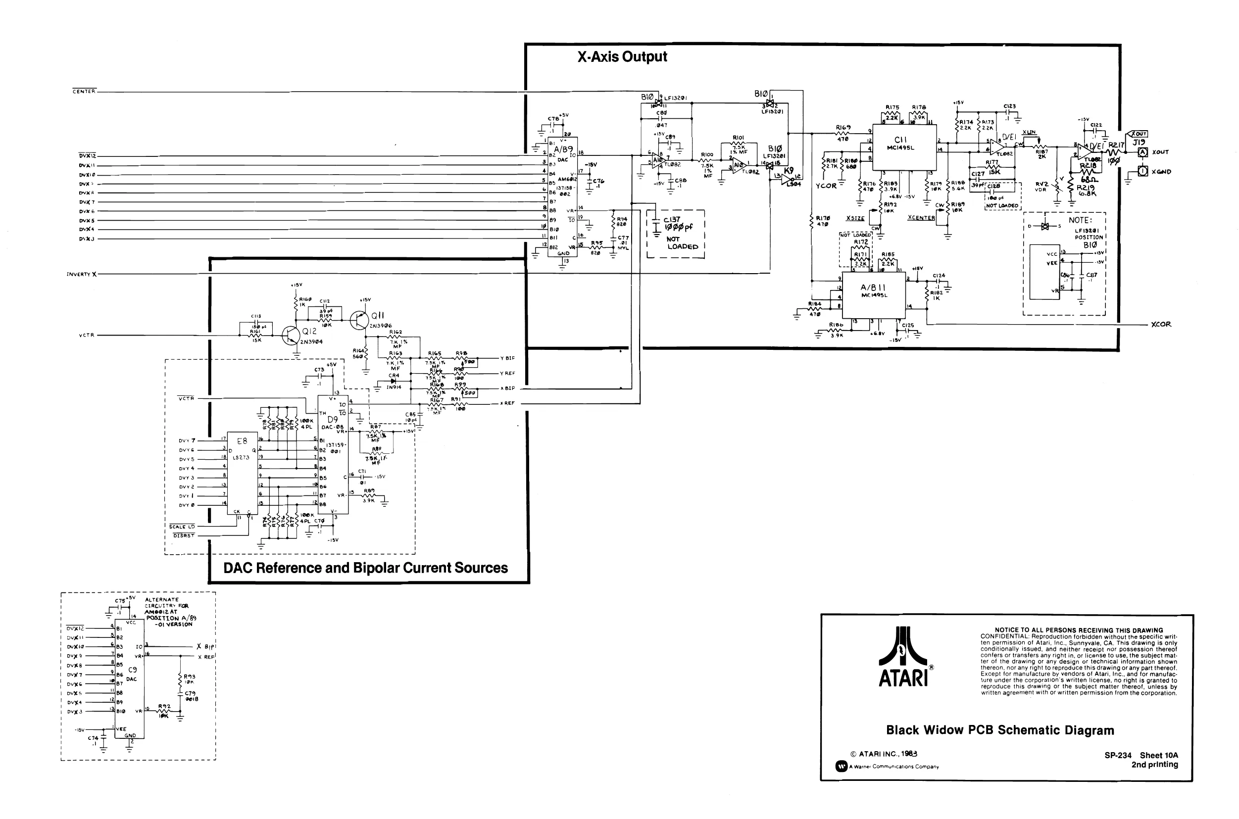
X-Axis Output
CENTER. 9 uFis201
RI75 R78 teiszay
ci Mci49se wee.
ovxit
wx
wx
DvxT
pve
ox: Dns
Dvxs
INVERTY X:
A/B I MC ra95L
‘a18 7 ase |
39K verR
ver . wReF
ove?
ove.
pws.
ovr
ows
ove
ove
rear) ' '
'
' '
'
H
i Hl i i { DIsRET
fl
ALTERNATE CIRCUITRY FOR Ameoiz AT POSITION A/89 ~01 VERSION
confers or transfers any right in, or license to use, the subject mat- NOTICE TO ALL PERSONS RECEIVING THIS DRAWING CONFIDENTIAL: Reproduction forbidden without the specific written permission of Atari, Inc., Sunnyvale, CA. This drawing is only
() conditionally issued, and neither receipt nor possession thereof
. ter of the drawing or any design or technical information shown thereon, nor any right to reproduce this drawing or any part thereof. Except for manufacture by vendors of Atari, Inc., and for manufac: ture under the corporation's written license, no right is granted to eproduce this drawing or the subject matter thereof, unless by written agreement with or written permission from the corporation,
Black Widow PCB Schematic Diagram
© ATARI INC., 1983 SP-234 Sheet 10A ware: Communcanons Company 2nd printing
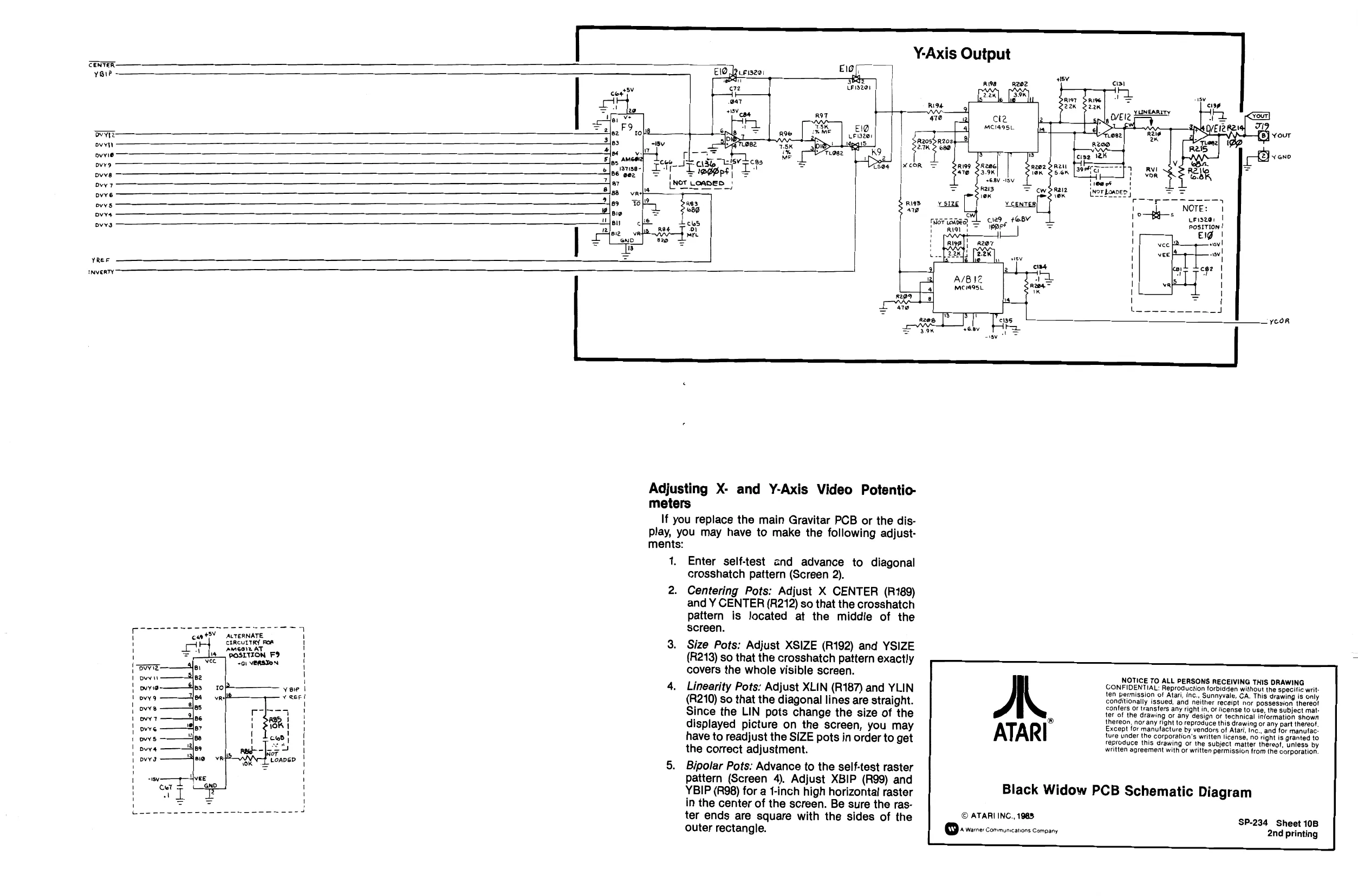
Y-Axis Output
CENTER: yeu
Drie ov ovvie pyro
bw? ovve ows ovys bys ee GS
ceisza: | POSITION! ENg | vee f asv! vee av!
yt tees aT 78 a
yRee INVERTY
yeoR
Adjusting X- and Y-Axis Video Potentiometers If you replace the main Gravitar PCB or the dis- Play, you may have to make the following adjustments: 1, Enter self-test and advance to diagonal crosshatch pattern (Screen 2).
- Centering Pots: Adjust X CENTER (R189) and Y CENTER (R212) so that the crosshatch pattern is located at the middie of the ee 7 screen. v
| ' | yall | Siesta | \ | 3. | Size Pots: Adjust XSIZE (R192) and YSIZE |
| H | + he “OStTHON ro | ' | (R213) so that the crosshatch pattern exactly |
fe Oe ease hat
| {owie——4fa | | | overs the whole visible screen. | oy | NOTICE TO ALL PERSONS RECEIVING THIS DRAWING |
| \ | 4. | Linearity Pots: Adjust XLIN (R187) and YLIN | ten permisslon-ot Ahan Ine Buryede Sa pee SpeCIC wrt |
(R210) so that the diagonal lines are straight. anters 0 anetoss sty ight nor necro oS eae eet Since the LIN pots change the size of the fs Jeol ihe degieng oF any aesign or technical intormation shown displayed picture on the screen, you may ATARI Excoot viovmanulaclur ty vendors Of Atarl Ine. and for manufac: have to readjust the SIZE pots in order to get reproduce this arawing or ine subject matter ingreot ware ts
weitten agreement with or written permission trom tne corporation
the correct adjustment. rien agreement wittror writ from th ti
- Bipolar Pots: Advance to the self-test raster pattern (Screen 4). Adjust XBIP (R99) and . . .
YBIP (R98) for a f-inch high horizontal raster Black Widow PCB Schematic Diagram ter ends are square with the sides of the © ATARI ING., 1985 SP-234 Sheet 10B
in the center of the screen. Be sure the ras-
outer rectangle. + v2r26: Communications Company 2nd printing
This page is a drawing, shown as the original scan.
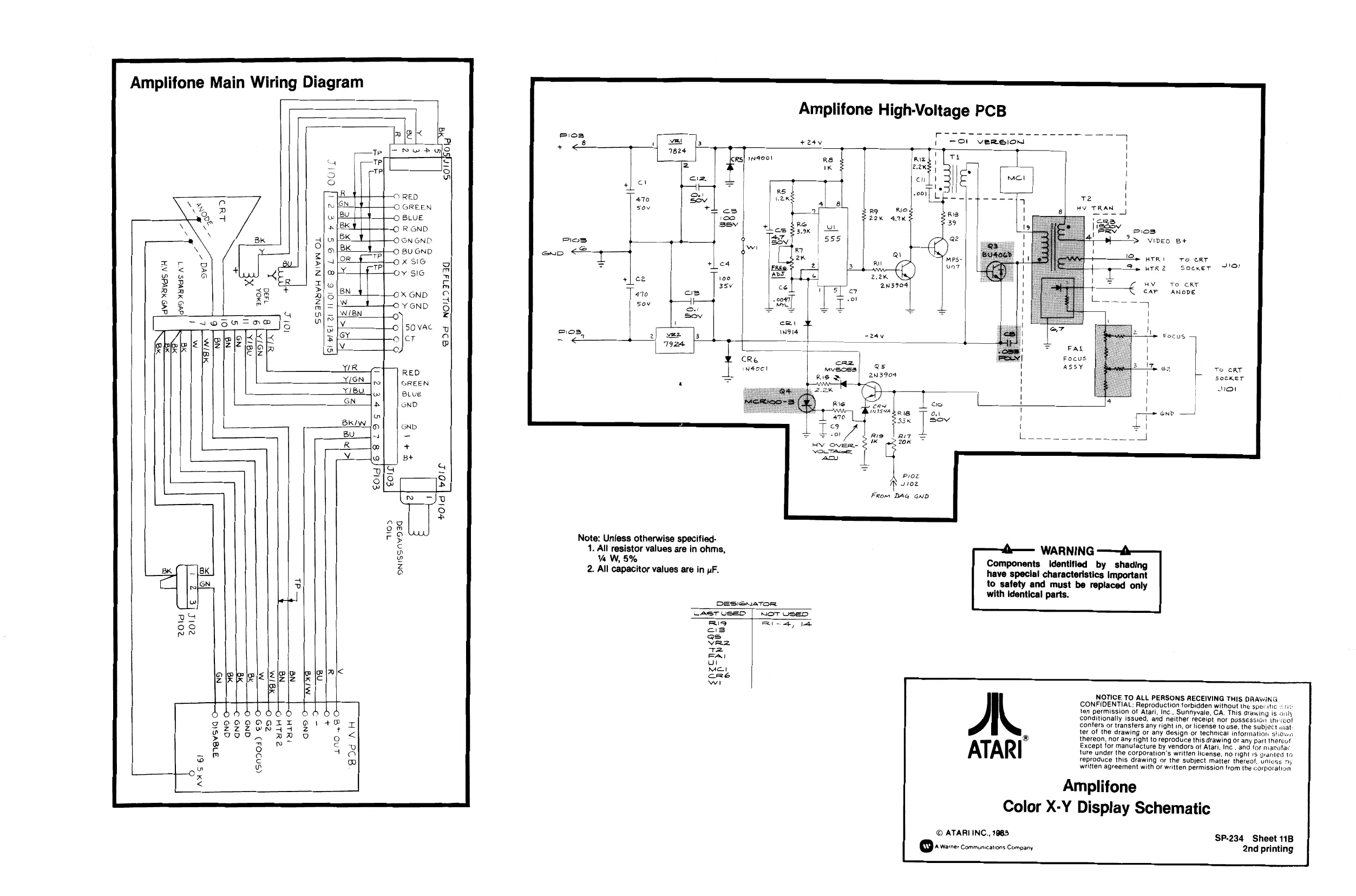
Amplifone Main Wiring Diagram
Amplifone High-Voltage PCB
poe-eseee Cl VERSION cl Pics 7 +e4y SOI SOld
CO! i re 1 e] HY TRAM |
A HTRI oro ert a8 2 2 Socker vier glosere = og uv oro cer ———* car anope. Lin dVO HSS AH Javo YvaS AT
SSANSWH NIVW OL
Gg [sivrer arto) dd NOILDINIII
socker
cay cio WISASRIB T 0.) 53x | SOV BT 9G +e 2
ld(6 8 iL| +0id| voir €Ol €01.
- All resistor values are in ohms, Ve W, 5%
- All capacitor values are in uF.
DESIcUATOR Ast useD [Not USED RID Rat, ie as as vR2 Te FAI ul Met ore wr mil WET
confers or transfers any right in, of license touse, the subject mat NOTICE TO ALL PERSONS AECEIVING THIS DRAWING CONFIDENTIAL: Reproduction forbidden without the sper tie «i: ten permission of Atari, inc., Sunnyvale, CA. This drawing is onl) conditionally issued, and neither receipt nor possession inv ico! ter of the drawing or any design or technical information shown zs 2uLH
® thereon, nor any right to reproduce this drawing or any part thereat
Except for manutacture by vendors of Atari, Inc , and for manutac
ture under the corporation's written license, no right 1s granted to reproduce this drawing or the subject matter thereo!. unless. ny written agreement with or written permission from the corporation ano No ano 1YLH Owevsia «snd04) €9
Amplifone
Color X-Y Display Schematic
© ATARIING., 1083 SP.234 Sheet 1B Qa warre: commumcations Company 2nd printing
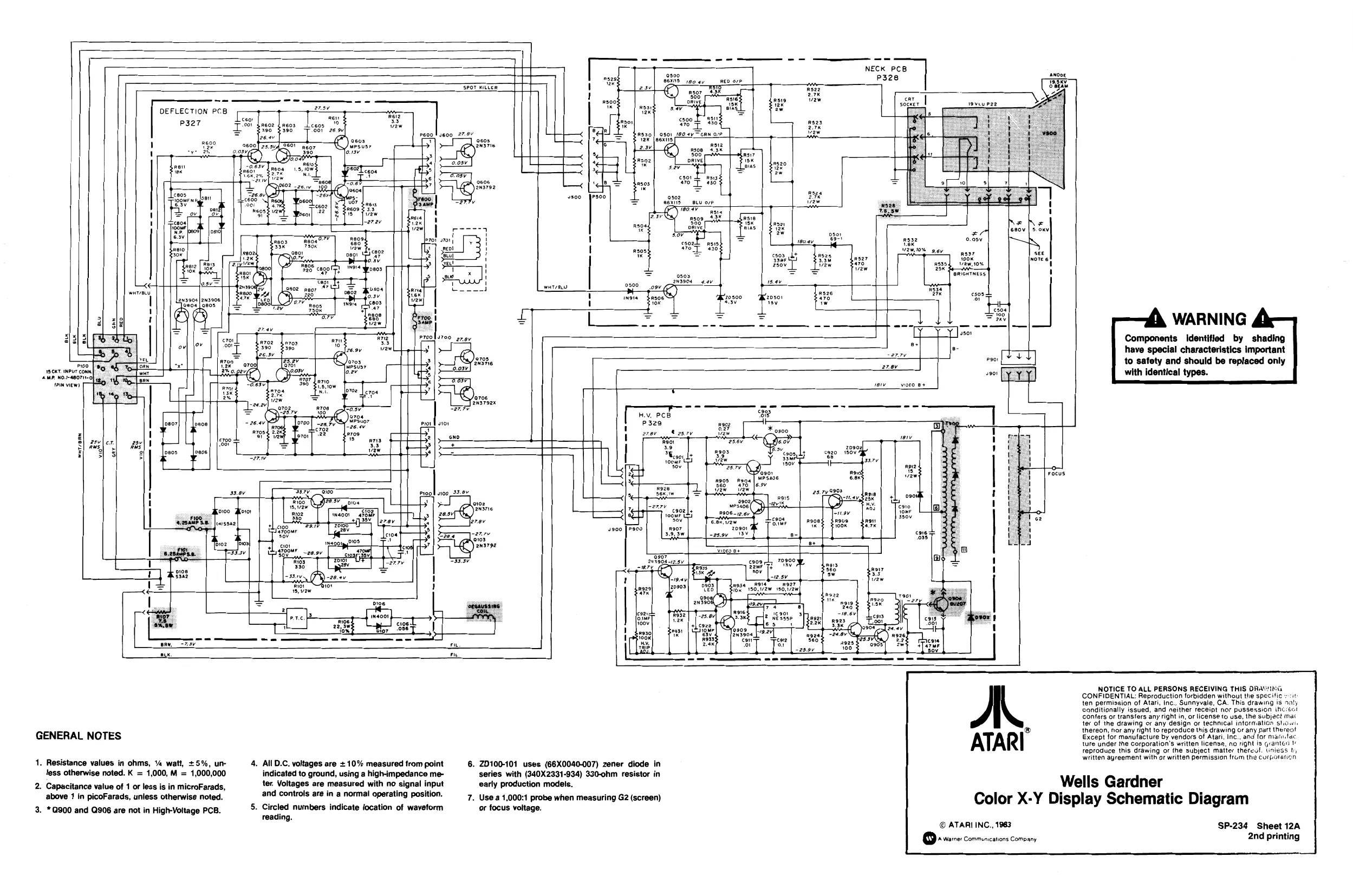
NECK PCB P3268 SPOT MLLER, nize
DEFLECTION PCB P327 eases ae 600! s6oo_27.0v
| | A r” 4 2.054
! wee oa y = oe oe + ‘) hl Apne 2.60 Rs37 see | Be notes
aqadg ot s wy tt UR WARNING
| 32} 8 | | | el | vet | Components Identified by shading | ||
| santy | e | T | have special characteristics important | |||
| 7a[re | ode | fe | sai | a | ro [+] | to safety and should be replaced only |
| “tee nmi | 2.080; | = | aver yy) 7. | with identical types. | ||
| reece | r8tv. | vik B+ |
T
re =
&| no
3 blue lt
e909; 70300, a Seo 5517 ses aa fi jasse 8514, noaT T 47 Se ssOcvew 180,724]
NOTICE TO ALL PERSONS RECEIVING THIS ORAY CONFIDENTIAL: Reproduction forbidden without the specific vit ten permission of Atari, inc., Sunnyvale, CA. This drawing is saly Conditionally rseued, and neither receipt nor pussession nt bet Contats of transfers any right in, orlicense to use, he Subject rat ferof the drawing cr any design of technica nication Sh.
thereon, nor any "ght to reproduce this drawing or any part tn
GENERAL NOTES Except for manviacture by vendors of Atari, Inc., and ior Mari.tac
ture under the corporation's written license, no right Is granten reproduce this drawing oF the subject matier theteut nies by atten agreement with or written permission from the Curparauicn
- Resistance values in ohms, % watt, 5%, un 4. A.C. voltages are +10% measured frompoint 6. ZD100-101 uses (66X0040-007) zener diode in
| Jess otherwise noted. K = 1,000, M = 1,000,000 | indicated to ground, using a high-impedance me- | series with (240X2331-934) 330-ohm resistor in | |||
| 2. Capacitance value of 1 or less is in microFarads, | ter Voltages are measured with no signal input | early production models. | Wells Gardner | ||
| above 1 in picoFarads, unless otherwise noted. | and controls are in a normal operating position. | 7. Use a 1,000:1 probe when measuring G2 (screen) | i: | i | i |
- #900 and Q906 are not in High-Voltage PCB. 5. Chola numbers indicate location of waveform or focus voltage. Color X-Y Display Schematic Diagram ing. © ATARI INC., 1983 SP-234 Sheet 12A Qe ware: communications Company 2nd printing