Missile Command Cocktail DP-152-1st-02A
Missile Command (rev 3, A035467-02/04 PCBs) (Atari, 1980) · Drawing Package · 1 pages · original scan
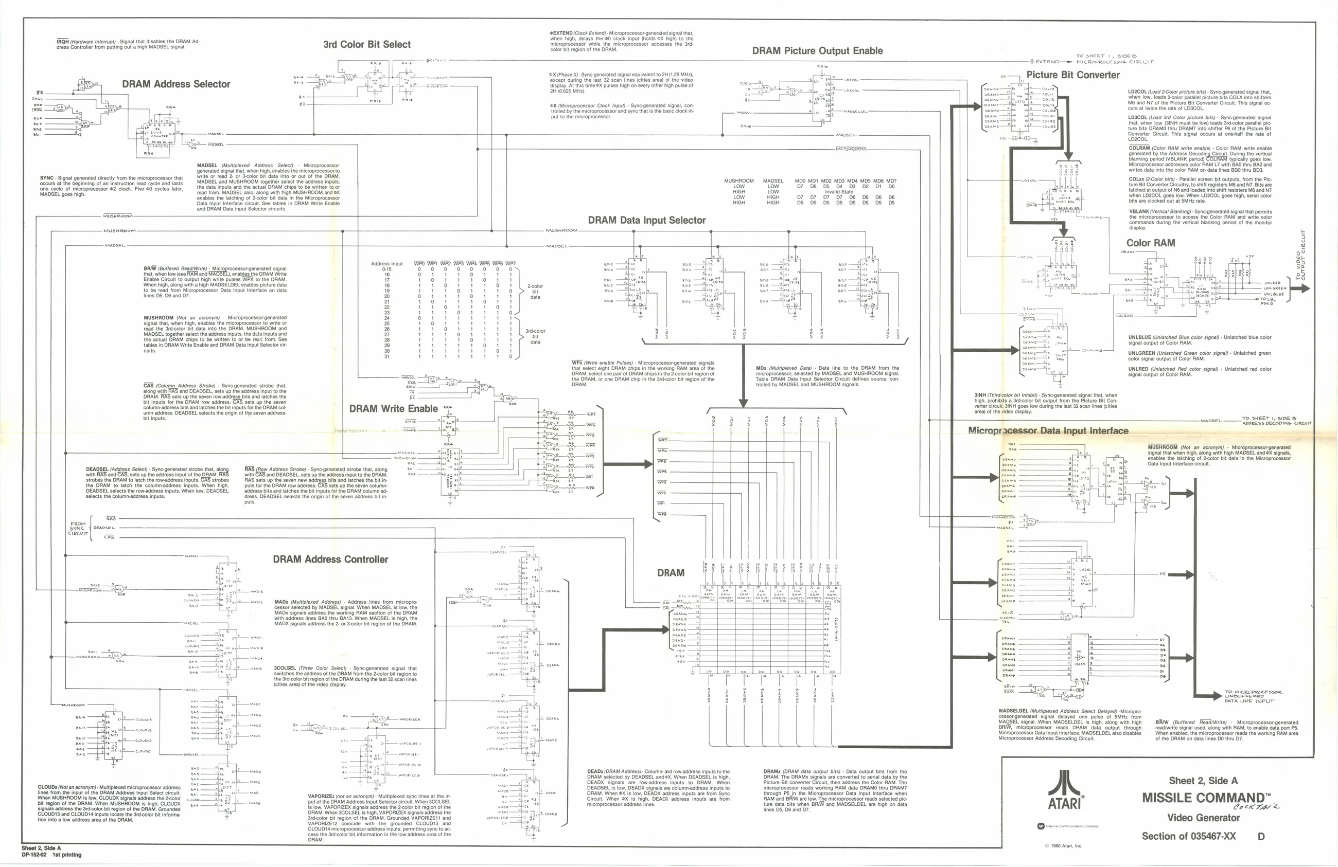
‘@EXTEND (Clock Extond)- Microprocessor generated signal that, lwhen. high, delays the 60 clock Input fnolds 60 hgh) to the Iicroprocessor while the microprocessor accesses the 3rd olor Bit region of the DRAM, TRH (Haraware nterupt) - Signal that dsables the DRAM Ad ‘ress Controller from putting out a high MADSEL signal 3rd Color Bit Select DRAM Picture Output Enable yo SHEET 1, sioce : BEXTEND—e MicROPRoCE'ssoR CIRCUIT ‘9X (Phase X)-Syne generate signal equivalent to 2H(1.25 Mia, a Picture Bit Converter ‘xcept during the last 32 sean lines (ees area of the vdeo coten. =] DRAM Address Selector ‘spay. ths time X pulses high on every ther high pulse of ee
| oefouss uta | oen. | 02604 Lowa 2Coter picture bts) - Syne generates signal hat |
when low, lds 2colr paral lture Bes COLX at shes 1s and 7 ofthe Pitre Bt Converter Ceut. This signal oc 20 (aieoprocessor Clock input) - Syne generate signal, con- a a of ere ‘trolled by the microprocessor and sync that is the basic clock in- hata tasgaening pul to the microprocessor LDSCOL Load a Color picture bits) - Syne-gonerated signa that when low GINH must be low loads Sre-olor paral ple swe {ure ite DRAM thru DRAM int shifter PB ofthe Picture i
| one | + | soe. | ‘Converter Crcut. This signal oocurs at Onehall the rate of |
5 toacor’
| eal | } | USSR | ZOTRAM (Color RAM write enable) - Cole RAM write enable |
gonerated by the Adcrose Decoding Creu. During the vertical Sinking period (VBLANK period) tical 908 on, IMADSSL. jlckGieied Adaned” sukey)-— reensoeebe Mcroproseasor adresses color RAM L? oh G0 ts Baa ‘generated signal that, when high, enables the microprocessor to ‘wattes cata Into the color RAM on dete nes GOO Rieu BO,
| SYNC - | Signal generated directly from the microprocessor that | ‘ite of reed :2. or S-cokot WR date Into or out of the ORAM. | ‘COLxx (2-Color bits) - Paraliel screen bit outputs, from the Pic | ||||||||||
| Staur a re Sepang ot'av atten ead se ane ats__-MADSEL and MUSHROOM together select the adress Imus, | MUSHROOM | —MADSEL | MOO MDX MD2 MOS MOS MOS MDB MO? | {ere Bt Gonvertr Crt, to suitrogiotors Band W?, Bis ae | |||||||||
| ne cyclo of microprocessor @2 clock Five 60 cycles later, | Re data inputs and the actual ORAM chips o be written to oF | A | a tone | pe ot os | latched at eutpu of NO and loaded into shit esstre Mand N? | ||||||||
| MARBET eo hy | tables the attng of bel tds the Mcroprosessr | tow | HIGH | Oy | oy | 7" | Oy | De | Ds | D8 | oe | Uis'ae docked ou ar sure | oN oer |
| Data Input Intertace circuit. See tables in ORAM Weite Enable | HIGH | HIGH | 05 | D5 | D5 | 05 | 05 | 05 | 05 | 05 | chee eos | ee |
‘nd DRAM Data nput Selector creat BLANK (Vortica! Blanking) Syne generated signal tat permits mameao, the micropecassor to aceese the Color RAM and wife color DRAM Data Input Selector Gemrande during the vertical Banking peed of the monitor
| mustimpon: | sausi@oom | " | * | . | ay. | 7 |
| nace | ‘ | panos. | Color RAM | a |
mane s
| Adceess input | PD WP VOPR (OPS WPA WPS PS WP? | ove | von | if | 2 | |||||||||
| RAW (Bfored ReglWrite)- Microprocessor generated signal | O18 | o | 0 | 0 | 0 | 0 | 0 | 0 | 0 | sd | I | woe | ||
| {hat when ow (68 PAM and | “enables the ORAM Wine | 6 | 03 | 330% | 4 | $ | qe | F | ||||||
| Enable Circuit to output high write pulses WRX to tho DRAM. | 7 | 10 | 1 | 4 | 404 | 4 | ee | vos —ten 3s, | ~ | |||||
| ‘When high, slong sith high MADSELDEL enables plture cata | % | +30 | 4 | 4 | 4 | 0 | tL | cece | we | wee | ah | i | ||
| to'be rand from hroprocessr Data pt Inert on data | Hy | Sn | ee | be | wt | |||||||||
| tines 05, Ds and OY. | 2 | re | ar | bes 3h | E | |||||||||
| Fy | tory | $ | O44 | woe | we | we | dj | |||||||
| 2 | Yor | 4 | 3 | OG | tts | ts | ||||||||
| a | yi | Soot | 4 | 30 | + | |||||||||
| MUSHROOM (ot an acronym) - Microprocessor generated | a | ora | trad | s | + | + | ||||||||
| Signal that, when high, enables the microprocessor to wie or | Fs | ,oy | tt | ad | ||||||||||
| toad the ecole | data info the DRAM. MUSHAOOM and | Fy | 130 | 4 | 4 | 4 | tt | | secoter | ine | ee | ty | aie | ||
| MADSEL together sloct the address inputs the data inputs and | Fa | ee | ee | ee | 33 | 3 | 33 | Reon | tohed | blue | color | |||
| the actual DRAM chips to be written to or be ree from. See | Ey | 444 | 4 | 014 | 407 | oy | v*? | S | il | 7 | Reais | Be | oer aaned = Urnced Cive | ox |
| {abies DRAM Wite Enable and DRAM Data Input Selector et | Fy | yaya | Fogg | |||||||||||
| cults. | = | erunupyrs | ys | mar | UNLGREEN (Uniatched Green color signal) - Unlatched green | |||||||||
| on | yor | pp | ao | toto | color signal output of Color RAM. |
[WE (ete enable Pulses) - Microprocessor generate signals
| that slet eight ORAM chips Inthe working RAM area of the | MDs (Multiplexed Data) - Data line '0 the ORAM rom the | LUNLRED (Unietched fed color signal - Uniatched red color | ||
| DRAW, solect one pairof DRAM chip inthe color bit region of | microprocessor, selected by MADSEL | and MUSHROOM signa. | Sina output of Color RAM: | |
| = | tho DRAM, of one DRAM chip Inthe Soir Bt rgion ofthe | ‘able DRAM Data input Select Grcult tines source, Con | ||
| ERS (Column Aairess Strobe) - Syne-genaated strobe that, | ki | 2 | ORAM. | troled by MADSEL and MUSHROOM signals. |
oats RAS and DEADSEL ets up te acre inp ote INH (Tol Bt In - Sy genes sgn tat, whan Bit inputs for tha BRAM row adress. CAS ste up te seven ig, prohits a Scolar bit output rom the Pte Bit Concolumnar is and itches the bit input or he ORAM co- seer goes lo rn wn 2s rien ‘umn address, DEADSEL selects the origin of the seven address: . .
| Ditinput. | 205 | 3 | 3 | 8 | 8 | Bos | t+ | saose.—— | TO, SHEET | SIPEG. | | |
| 253 | fF | tee | sg | Roomass oedopnue | emeor |
co ‘USAROOM (Wor an acronym) - Microprocessor generated
| 4 | mansen. | = | signal that when high, along with high MADSEL and OX signals, | |||
| nto: | bie | rabies the latching of 2colr it data in the Microprocessor | ||||
| pre | + | [ | pei | 2 | Bata input Interface chet | |
| DEADSEL (Adgass Select -Syne-gonarates sttobe that, | IS oy Assos Srobe- | Sy ginaated srbe that, slong | tes sla“ | tae} | =e | a |
| with RAS and CAS, sets up the address input of the DRAM. | with CAS and DEADSEL, sets up the address input to the DRAM. | w—- | _————_} | Fy | ||
| ‘oboe the DRAM to atch the rowadérse inputs CAS strobes | RAS sete up the soven haw adaae bie and etches the Bt i | i | a | a | ||
| {he DRAM to latch tho columadaross Inputs. When high, | puts forthe DRAM row address. GAS ses p the sven column | Rae | ||||
| DEADSEL soecs the rowaddress Input | When low, DEADSEL | address Bits and latches the itinputs forthe DRAM column 8 | rat) | wz |
‘soiects the columaddress input. ress. DEADSEL seocs the origin ofthe seven adress it puts e as EB FARE | oeaoser. Eton |
| DRAM Address Controller | he | 23 | |||||
| DRAM | He | tf | |||||
| a) | oon | “ | Kn | ||||
| }i—wana | MADx (Multiplexed Address) - Address lines trom micropro- | fm | —8 | i | a | Bre | S| |
| ‘cessor selected by MADSEL signal When MADSEL Is low, ho | ape | l= | |||||
| WMADx signals adress the working RAM section o he ORAM | asco | | | |||||
| L | ‘with adotoss lines BAO thu BAYS. When MADSEL i high the | sess | rar | ||||
| ‘MADX signals address the 2 or ol: roion ofthe ORAM. | Ponca | = | keg |
+ > |
| SCOLSEL (Tiree Color Select) Syne generated signal that | = | = |
Stones the assess ofthe DRAM fom the ol bt region to a {ho Secor Bi rogion of he ORAM during the ast 32 can ines
| {oties ara) of thewdeo dpay. | | | tol |
| i | pd | meee |
| 3 | é | BR Uwe IeUT |
NADSELDEL (Multiplexed Address Solect Delayed) Micropro: C2ssorgenerated. signal delayed one pulse of SMHZ trom MADSEL signa. Witen MADSELDEL is high, along with high BRIW (Buffered Read/Write) - Microprocessor-generated |, tictoprocessor reads ORAM: dala’ output through _readwrite signal used, along with RAM, to enable data port PS. Microprocessor Data Input Interface. MADSELDEL also dsables When enabled, the microprocessor reads the working RAM area Microprocessor Address Decoding Creu. ‘of the DRAM on data lines DO the D7 Peon
CLOUDx (Not an acronym) - Multiplexed microprocessor adress lines trom the input of the DRAM Addross Input Selct clcult. ‘When MUSHROOM is iow, CLOUDX signals adress the 2color Dit region of the ORAM. When MUSHROOM high, CLOUOX: Signals address the 3r-color bit region of the DRAM, Grounded ‘CLOUDIS and CLOUDI4 inputs locate the Sedcoler bit information into alow address aren of the DRAM. \VAPORIZEs (not an acronym) - Multiploxed syne lines atthe in puto! the DRAM Address Input Selector circult When SCOLSEL. Is low, VAFORIZEX signals adaress the 2coler it region ofthe DRAW. Whon 3COLSEL is high, VAPORIZEX signals address the Srdcolor Bit region of the DRAM. Grounded VAPORIZE'Y and VAPORIZE'2" coincide ‘with the. grounded CLOUD'3. and CLOUD 14 microprocessor adaress inputs, permiting sync to ac- {eee the Seal bit information inthe low adress area ofthe RAM: ‘Sheet 2, Side A DP-15202 tt printing DDEADx (ORAM Address): Column and row address inputs to the DRAM selected by DEADSEL andX. When DEADSEL 1s high, DEAOX signals ate. rowaddress inputs to. DRAM. When DEADSEL is low, DEADX signals we columeaddress inputs to DRAM. When @X is low, OEADX aairess Inputs are trom Syne Gircuit_ When @X is igh, DEADX address Inputs are fom ‘microprocessor adress lines, DRAMx (ORAM data output bits) - Data output bits fom the DRAM The ORAM signals are converted to serial data by the Picture Bit converter Cirult, then address the Color RAM. The ‘microprocessor reads working RAM data ORAMO thru ORAM? {hough 5, In the Microprocessor Data Input interface when RAM and BAIW are low. The microprocessor eads solectd pi ture data bits when BRUW and MADSELDEL are high on data lines 05, D6 and O7 ATARI"
© 1660 Ata, ne. Sheet 2, Side A MISSILE COMMAND™ Coen Ta & Video Generator Section of 035467-XX D