Red Baron Sit-Down DP-171-1st-02B
Red Baron (revised hardware) (Atari, 1980) · Drawing Package · 1 pages · original scan
Option Switch Inputs
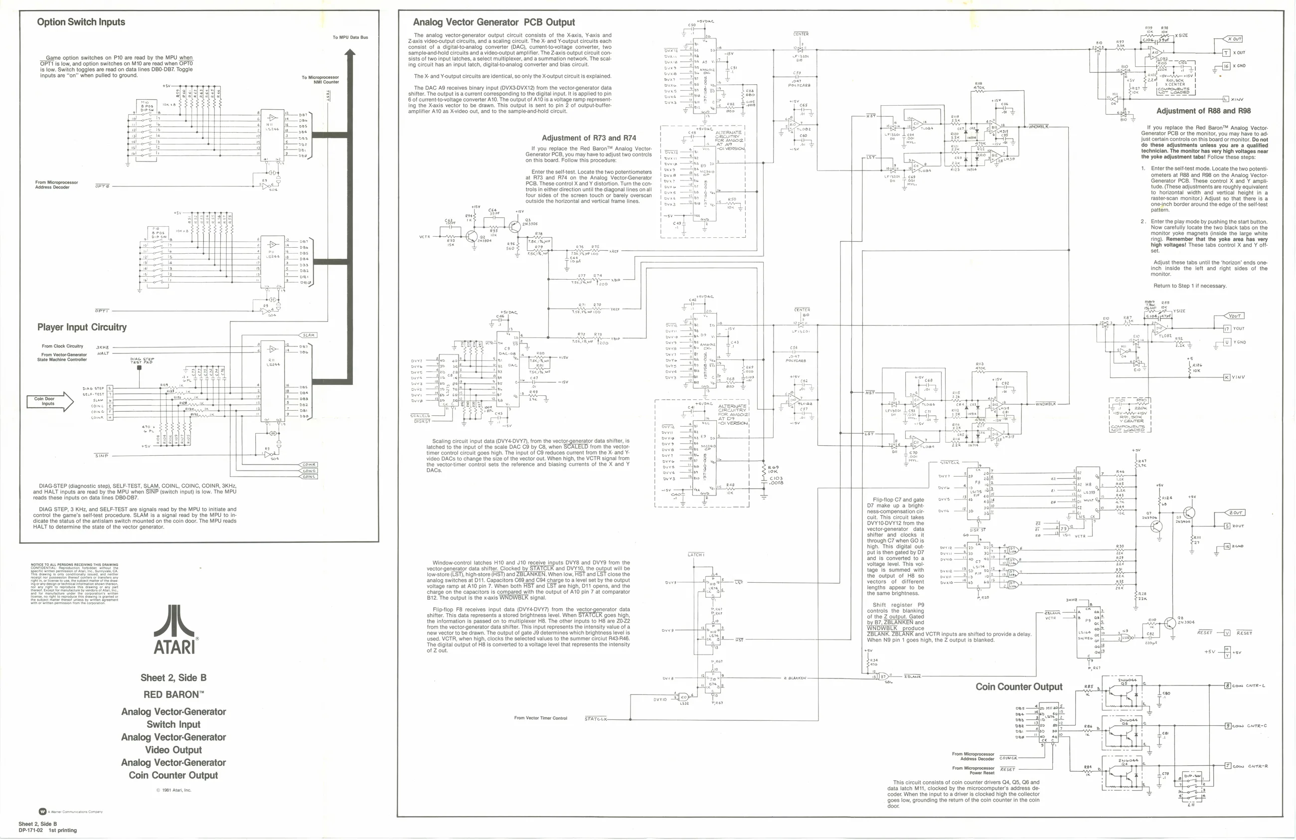
Game option switches on P10 are read by the MPU when. PTT 1s fow, and option switches on MTO are read when OPTO is low. Switch toggles ae read on data lines DB0-DBY. Toggle inputs are “on” when pulled to ground. Analog Vector Generator PCB Output ‘The analog vectorgenerator output circuit consists of the Xaxis, Yaxis and Zaxis video-output circuits, and a scaling circuit. The X: and Y-output circuits each ‘consist of a digitarto-anaiog converter (DAC), current-tovoltage converter, two sample-and-hold circuits and a video-output amplifier. The Z-axis output circuit consists of two input latches, a select multiplexer, and a summation network. The scaling circuit has an input latch, digitalto-analog converter and bias circuit. ‘The X-and Y.output circuits are identical, o only the Xoutputcircult is explained. ‘The DAC AS rec shifter. The output (es binary input (OVX3-DVX12) from the vector-generator data ‘a current corresponding to the digital input. tis applied to pin EB) xn Sot currentsovotage converte At0.The ouput of AIO is a watage ramp present ing the Xaxls vector to be dawn. This output fs sent to pin 2 of outputbutfer. amplifier 0 as Xvideo out, and tothe sample-andholdelreut Adjustment of R88 and R98
Sa IY you replace the Red Baron"™ Analog Vector. cae prema | Generator PCB or the monitor, you may have to 8d-
| Adjustment of R73 and R74 | Sere | just certain controls on this board ox moniter Da not |
' do these adjustments unless you are a qualified lhaaumpiac the Red Baron™ Analog Voce technician. Te monitor has very high voltages near enerator PCB, you may have to adjust two contrls the yoko adjustment tabs! Folow these stops ‘on this board. Follow this procedure: ae fa
| nor | in | sitet Locate he wo | potentometes | 1 | 1. | Enter the sottest mode, Locate the two potent |
| nter the elftest. | Loca | a | H | ‘meters at Ra and R96 on the Analog Vector | ||
| at RTS. and R74 on the Analog VectorGenerabor | i | Gonortor PCB, These contol X ana omplh | ||||
| From Wseposesor | PCB. These control X and | distortion, Turn the cen | H | Hae | iien cauteoninaetacian | anions |
| ‘rons Oneoer | trols in either dection unt the diagonal lines onal | | S"2 aN | fk L| | Eat een cde omen me uahiy canter | ||
| {our sides of the screen touch or barely overscan | | 2°75 ats | § | f= | rastorscan monitor) Adjust a0 that tere fo @ | ||
| outside | the horizontal and vertical frame lines. | 525 | ‘neinch border around the edge ofthe selttest |
oH one
| ' | 2. | Enter the play mode by pushing the stat button. |
\ Now carefully locate the two Black tabs on the ! monitor yoke magnets (inside the large white vera fing). Remember that the yoke area has. very high voltages! These tabs Control X and Y off ner set
- ‘Adjust these tabs until the ‘horizon’ ends oneinch inside the left"and right sides of the a ‘monitor ‘roo ™ Retum to Step 1 if necessary.
Paes oPrT Tak wr co YE
| Player Input Circuitry | ° | Ly | ~ |
fe Tae ios OP Leas
| From Glock Creuity — sxnz | fp | [> | i | ||
| From VectorGenerstor | HALT | Wp | le | ey | |
| i | any | 4 | Se a | ||
| conc | [E | ‘s | H | a | ATR |
| come [F | : | ! | Bepconl | ||
| peed! | — | \ | ac | eeat | |
| ms | al | Hl | “Verse! | ||
| ue | ! | ' | car. |
Scaling circuit input data (OVY4DVY7, from the vectorgenerator data shitr, is 1
| “ | fe | latched | te nput ofthe seale DAC C8 by GB | non SEALELD from the vector. | | | i |
| — | cars | video DACs to change the size of the vector out. When high, the VCTR signal from | 1 | |||
| em | {he vectortimer control sets the reference and Basing currents of the X and Y | ' | in | cee | ||
| Dace. | ' | od | > | |||
| Soa] | ! | 1 | Bio | ew | Ie | 5 |
| m | So | a | ||||
| DIAG-STEP (diagnostic step), SELF-TEST, SLAM, COINL, COINC, COINR, KHz | I | set | + | pe | AN | 7 |
| and HALT inputs are read by the MPU when SINP (switch input) is low. The MPU | 1 | 0x | T | is | ||
| teads these inputs on data ines DBO.DEY,. | ' | l= | Fliptiop C7 and gate | ‘ | = | |
| L | J | ‘07 make up a bright | lo | |||
| DIAG STEP, 9 KHz, and SELF-TEST are signals ead by the MPU to initate and | nese compensetion ait: | Ir |
contol the game's self-test procedure. SLAM Is a signal read by the MPU to ult This circuit takes
| Gicate the status ofthe antistam switch mounted on the coln door, The MPU toad | SiODYYEd tom the | z—4 |
| HALT to determine the state of the vector generator. | Yectorgenerator “data | hs |
Shiter and clocks. it {trough 7 when GOs high. This digital out putis then gated by 07 Band is converted to. ee ee Window-contrl laches H10 and J10 receive inputs OVY8 and OVY9 from the Yoltage level. This vol
| seorgcnate eamenermn enters | : | vectorgenerator data shite, Clocked by SYATCLK and DVY10, the output will be | lage ts summed with |
| ow-store (LST), high-store (HST) and | ZBLANKEN. When low, HST and LST close the | the output of H8 so | |
| analog switches at D1, Capacitors O89 and C94 charge to aleve set by the output | ows | ew | vectors of different |
| voltage ramp at A10 pin 7. When both HST and LST are high, 11 opens, and the | ele | lengths appear to be |
‘charge on the capacitors is compared with the output of A16 pin 7 at comparator res the same brightness. B42, The output le the axis WNOWELK signal Shift register, Po Fliptop F8 receives input data (OVY4OVY7) from the vectorgenerator data be controls the Blanking
| shifter. This data represents a stored brightness level. When | goes high, | a | of the Z output, Gated |
| the information is passed on to multiplexer HB. The other inputs to HB are 2023 | le | BY, ZSCANKER and | |
| {rom the vector generator data shifter. This Input represents the intensity value ofa | cos | WADWBLE | produce |
| new vector tobe drawn. The output | of gate J9 determines which brightness level is | BLANK | and VCTR inputs are shifted to provide a delay |
ls Used: VCTR, when high, clocks the selected values to the summer eciut RASA ‘When NS pin 1 goes high, the 2 output is blanked ATARI ‘The digital output of H8 is converted toa voltage level that represents the intensity of Zout oa
| Sheet 2, Side B | aoa | a | al |
Coin Counter Output RED BARON™ ons — Af na Analog Vector-Generator so he el
| log Vector-Generato! | Femail | SFE | geste |
| Switch Input | see | ot | Tian cvre-e |
Analog Vector-Generator oe Video Output From Microprocessor —__ “Asse Cocose SOTVER- Analog Vector-Generator rem cor ZT com enra-e m r Out F ‘This circuit consists of coin counter drivers Q4, Q5, Q6 and data latch Mii, clocked by the microcomputers address de- © 1061 Ata, ne Coder. When the input to a driver is clocked high the collector, {9028 low, grounding the return of the coin counter in the coin door
‘Sheet 2, Side B DP-171.02 ‘st printing