Asteroids DP-143-7th-01B
Asteroids (rev 4) (Atari, 1979) · Drawing Package · 1 pages · original scan
POWER INPUT
Sheet 1, Side B DP-143.01 7th printing CLOCK CIRCUIT
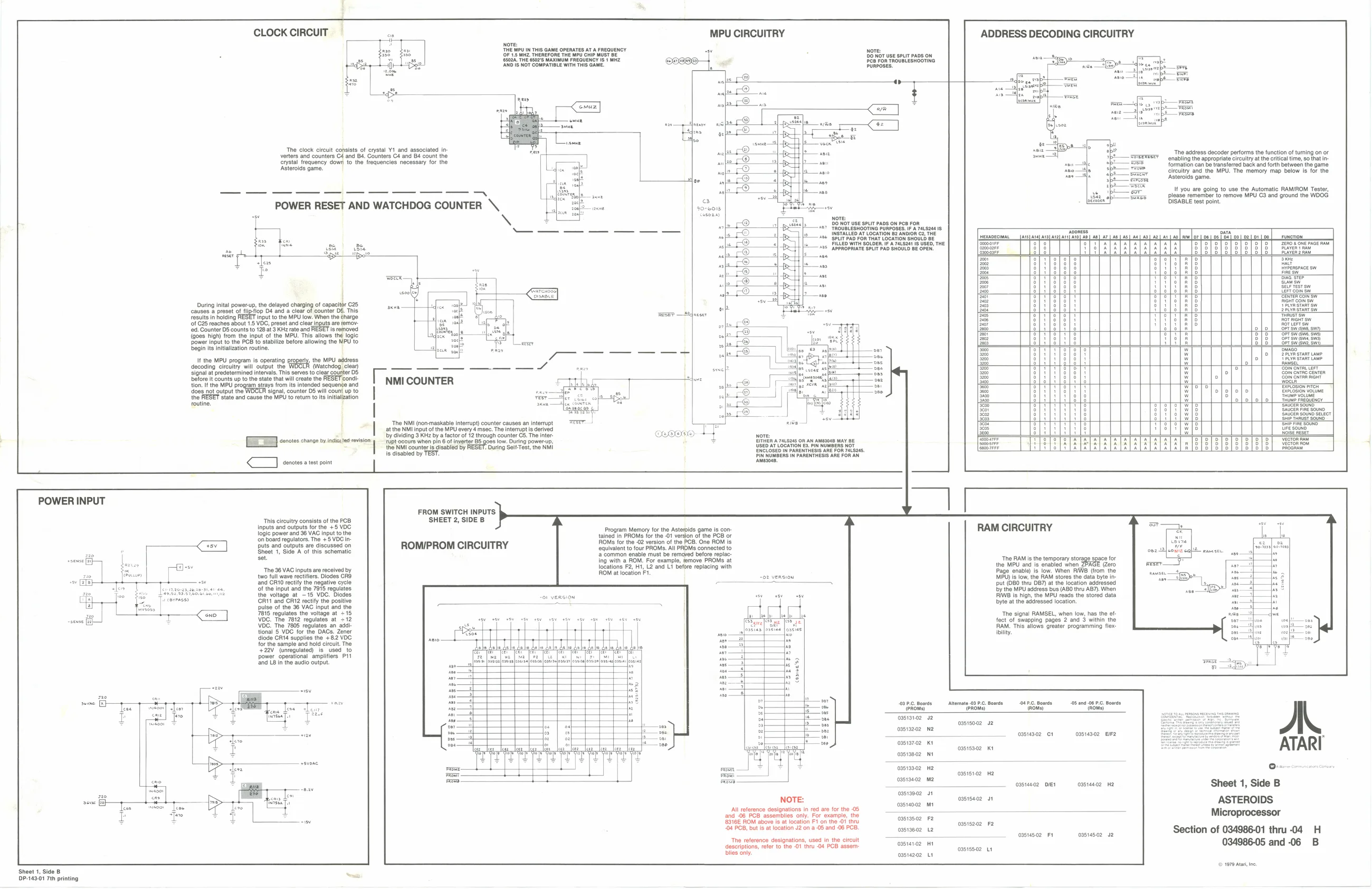
‘The clock circuit consists of crystal Y1_and associated inverters and counters C4 and 4. Counters C4 and 84 count the frequencies necessary for the
ee POWER RESET AND WATCHDOG COUNTER \, Nore
wel fia Sha, a Spe pte
is
During inital power-up, the delayed charging of capacitor C25 causes a preset of flipiop D4 and a clear of counter DE. This, fesults in holding RESET input othe MPU low. When the charge ‘of ©25 reaches about 1.5 VOC, preset and clear inputs are temov- ‘ed. Counter DS counts to 128 at 3 KHz rate and RESET Is removed (goes high) from the input of the MPU. This allows the logic ower input to the PCB to stabilize before allowing the MPU to begin its initialization routine.
the MPU address (Watchdog clear) It the MPU program is operating decoding circuitry will output the signal at predetermined intervals. This serves to clear counter D5 betoreit counts up to the state that will create th "cond tion. If the MPU program strays from its intended sequence and ‘does not output the: ‘signal, counter D5 will count up to the ‘state and cause the MPU to retum to its initialization routine,
donotes a test point
This circuitry consists of the PCB. Inputs and outputs for the +5 VDC logic power and 36 VAC input to the (on board regulators. The +5 VDC in puts and outputs are discussed on Sheet 1, Side A of this schematic set ‘The 36 VAC inputs are received by two full wave rectifiers. Diodes CRO and CR10 rectify the negative cycl Of the input and the 7915 regulates the voltage at —15 VDC. Diodes CRIT and CRI2 rectify the positive pulse of the 36 VAC input and the 7815 regulates the voltage at + 15 VDC. The 7812 regulates at +12 VOC. The 7805 regulates an additional 5 VDC for the DACs. Zener diode CR14 supplies the +82 VDC for the sample and hold circuit. The +22V (unregulated) is used to power operational amplifiers P11 and LB in the audio output Tt COUNTER
onotes change by indicted revision | Se — ee
‘The NMI (non-maskable interrupt) counter causes an interrupt at the NMI input of the MPU every 4 msec. The interrupt is derived by dividing 3 KHz by a factor of 12 through counter C5, The inter- ‘apt eccure when pin of verte BS gors iow. During power, the NMI countor is disabled by ‘During Self-Test, the NM Is disabled by TEST.
FROM SWITCH INPUTS SHEET 2, SIDE B
ROMIPROM CIRCUITRY OD MPU CIRCUITRY THE MPU IN THIS GAME OPERATES AT A FREQUENCY a OF 1's MHZ. THEREFORE THE MPU CMP MUST BE. Ssa2A, THE 6602S MAXIMUM FREQUENCY IS 1 MHZ SANDS NoT COMPATIBLE WITH THIS GAME.
ee 20-6018,
FEST —A%decaer
Nove: EXHER A 7416245 OR AN AMG04B MAY BE USED AT LOCATION E®: PIN NUMBERS NOT [ENCLOSED IN PARENTHESIS ARE FOR TauS2e6. PIN NUMBERS IN PARENTHESIS ARE FOR AN INSTALLED AT LOCATION B2 ANDIOR C2, THE. #8 SPLIT PAD FOR THAY LOCATION SHOULD BE FILLED wirl SOLDER IF A S24 5 USED, THE +35 PPROPRIATE SPLIT PAD SHOULD BE OPEN: ‘The address decoder performs the function of tuning on or ‘enabling the appropriate circuitry at the critica time, so that in- {formation can be transferred back and forth between the game girly and the MPU. The memory map below Is forthe steroids game.
If you are going to use the Automatic RAMIROM Tester, please remember to remove MPU C3 and ground the WOOG DISABLE test point
Eee
tee con ow
BRLIRSTAnT SW rormanr sw Ser Sse SH) ‘Spr swig Sw
gue ERouENer SSSRESCESSSIGEESIESES|EESIS Nose RESET leze|zezeleese|eazaleeze[>oz|>222|z222]2200]2225|
i H : vector ow
Program Memory for the Asteroids game is con tained in PROMs for the -01 version of the PCB or OMS for the -02 version of the PCB. One ROM is ‘equivalent to four PROMS. All PROMS connected to ‘a common enable must be removed before replac- 19 with a ROM. For example, remove PROMS at locations F2, H1, L2 and Lt before replacing with FIOM at location Ft RAM CIRCUITRY
‘The RAM is the temporary st 2 for the MPU and is enabled when Zero, Page enable) is low. When RIWB (from the MPU) is low, the RAM stores the data byte input (DBO thru DB7) at the location addressed by the MPU address bus (ABO thru AB7). When IMB Is high, the MPU reads the stored data byte at the addressed location.
The signal RAMSEL, when low, has the effect of swapping pages 2 and within the RAM. This allows greater programming flex. ibiity
0 Pc Bosse 047.6. Boards 05 and.06 PC. Boards (enoM. (mows) {Ronis}
ossista2 v2 ossisoa2 J ossis202 Na oa5149.02 ct ossiaso2 eIF2
‘The reference designations, used in the circuit descriptions, refer to the -01 thru -04 PCB assem: bilies only 036197.02
oasie02 Ki
nt
03513802 Ha oasist02 2 oasige02 m2 ossie02 Diet osstaco2 He 03519002 Jt 0515402 st oasao02 mt
ossias02 F2 oasiszoz F2 ossis602 2 oast45-02 FI osi4sc2 42 oapist02 Ht 0515802 U1 oasi4z02 Lt Sheet 1, Side B
ASTEROIDS Microprocessor
Section of 034986-01 thru 04 H 034986-05 and -06 B
(© 1979 Ata, ne