Gauntlet SP-284 1st Printing
Gauntlet (rev 14) (Atari Games, 1985) · Schematic Package · 26 pages · 23 sections · original scan
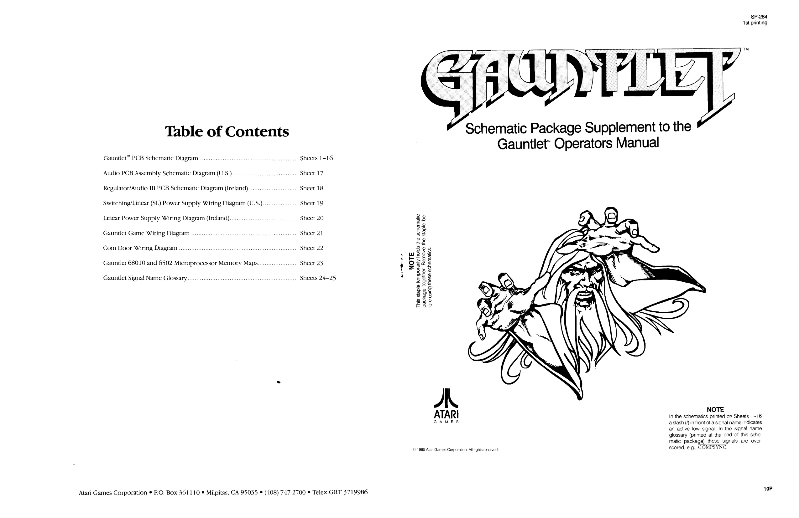
This page is a drawing, shown as the original scan.
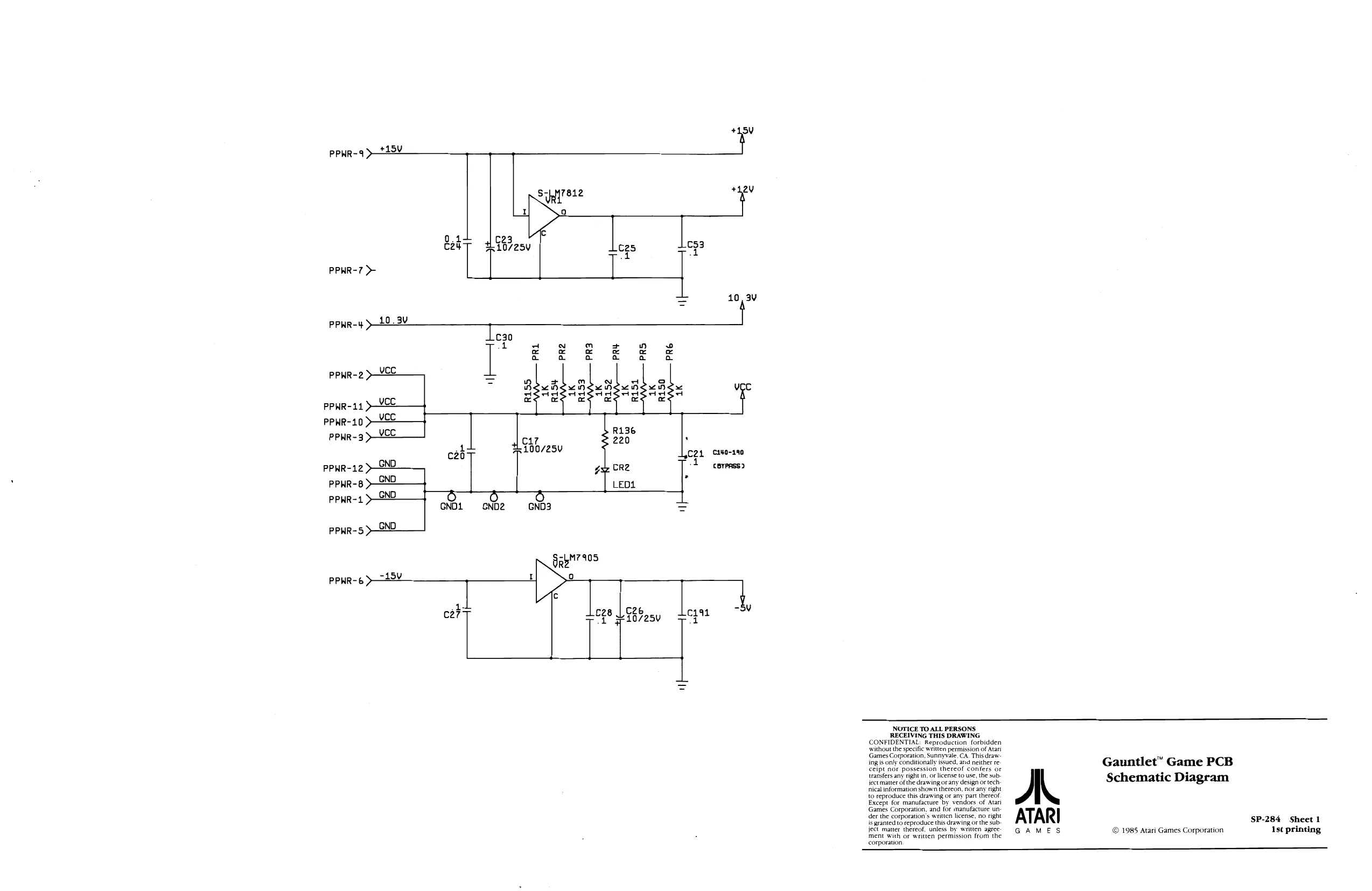
This page is a drawing, shown as the original scan.
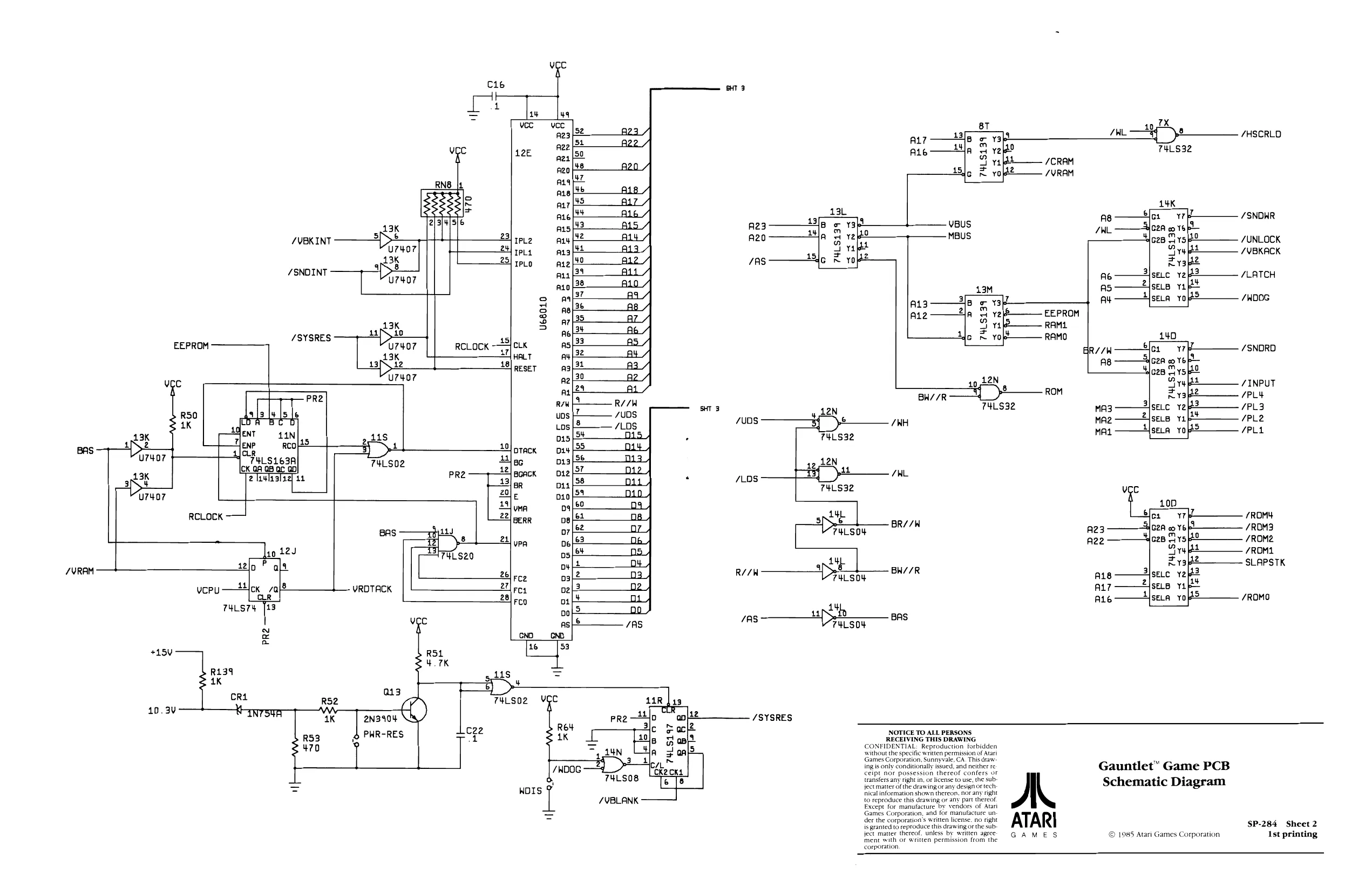
This page is a drawing, shown as the original scan.
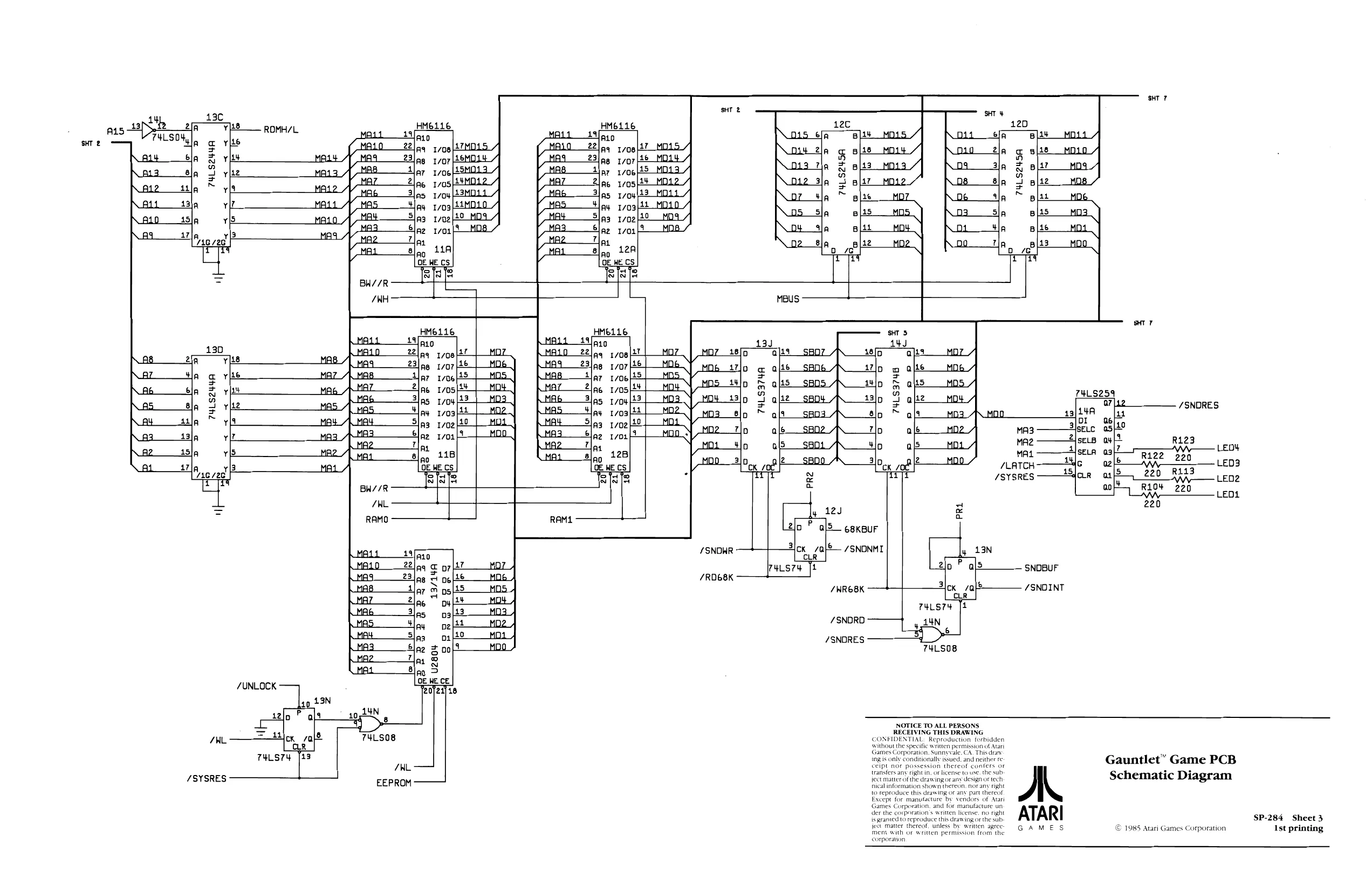
This page is a drawing, shown as the original scan.
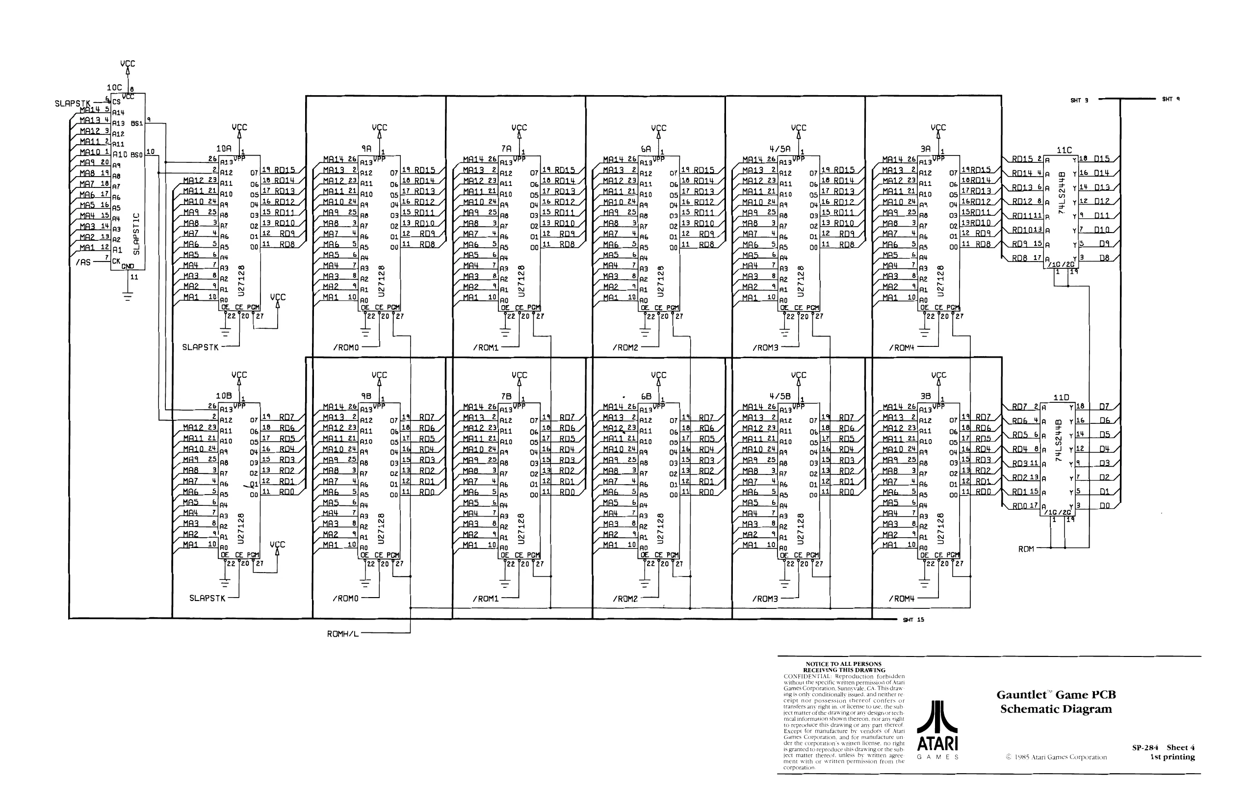
This page is a drawing, shown as the original scan.
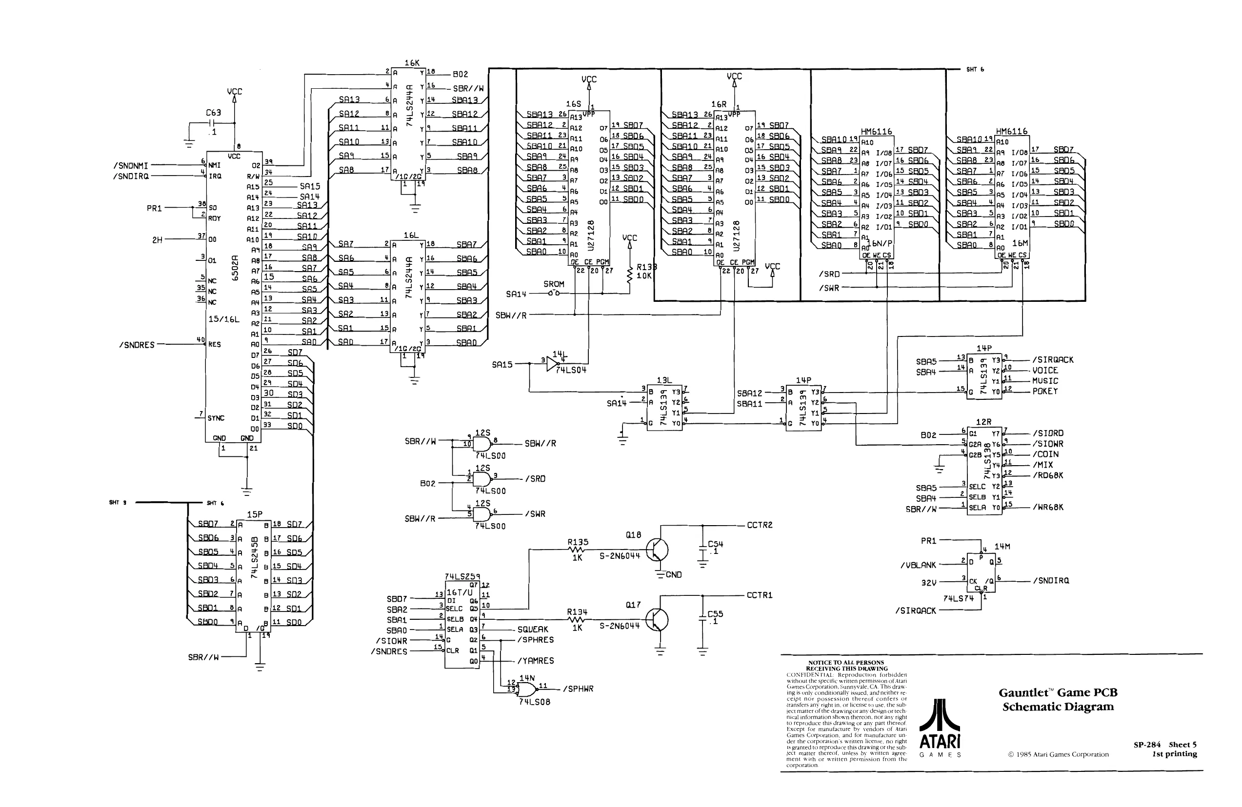
This page is a drawing, shown as the original scan.
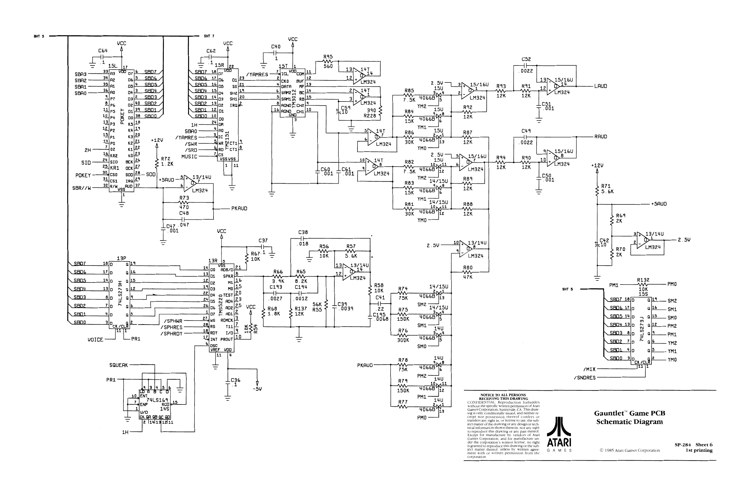
This page is a drawing, shown as the original scan.
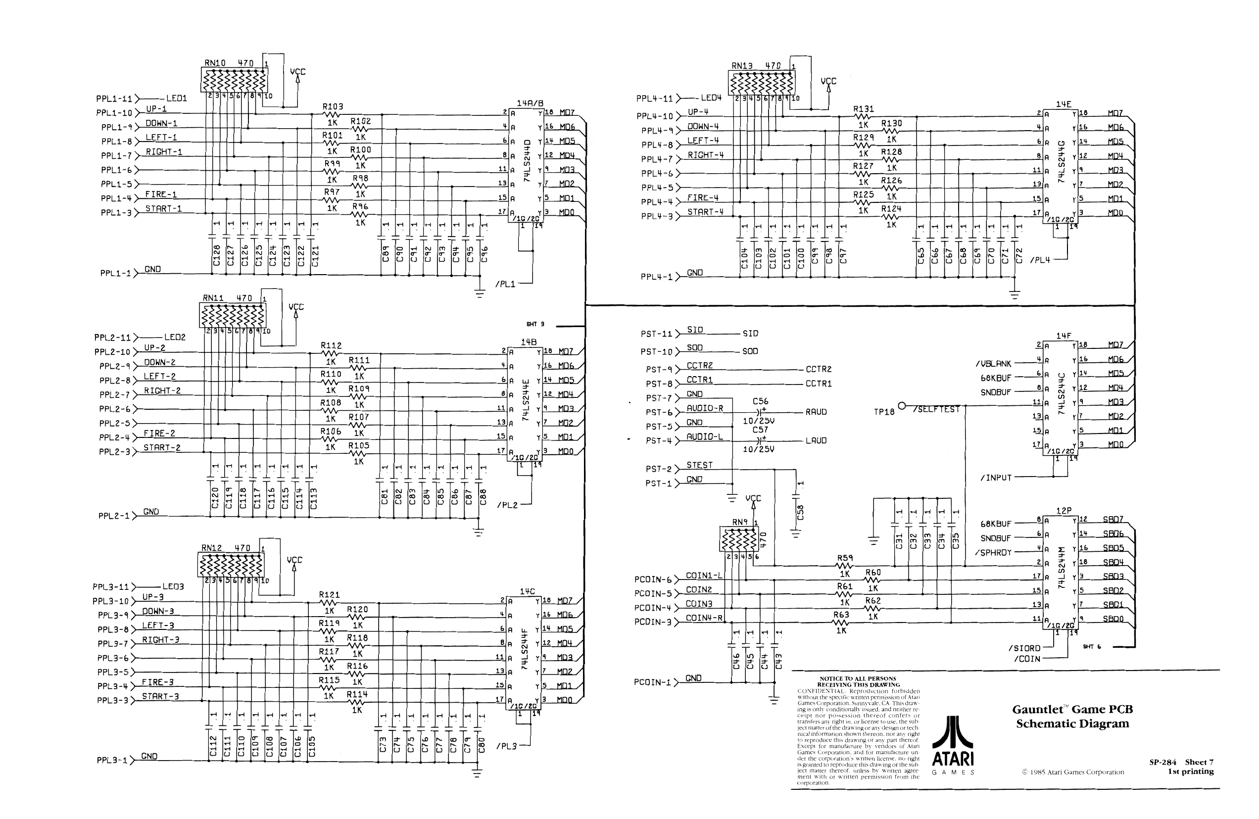
This page is a drawing, shown as the original scan.
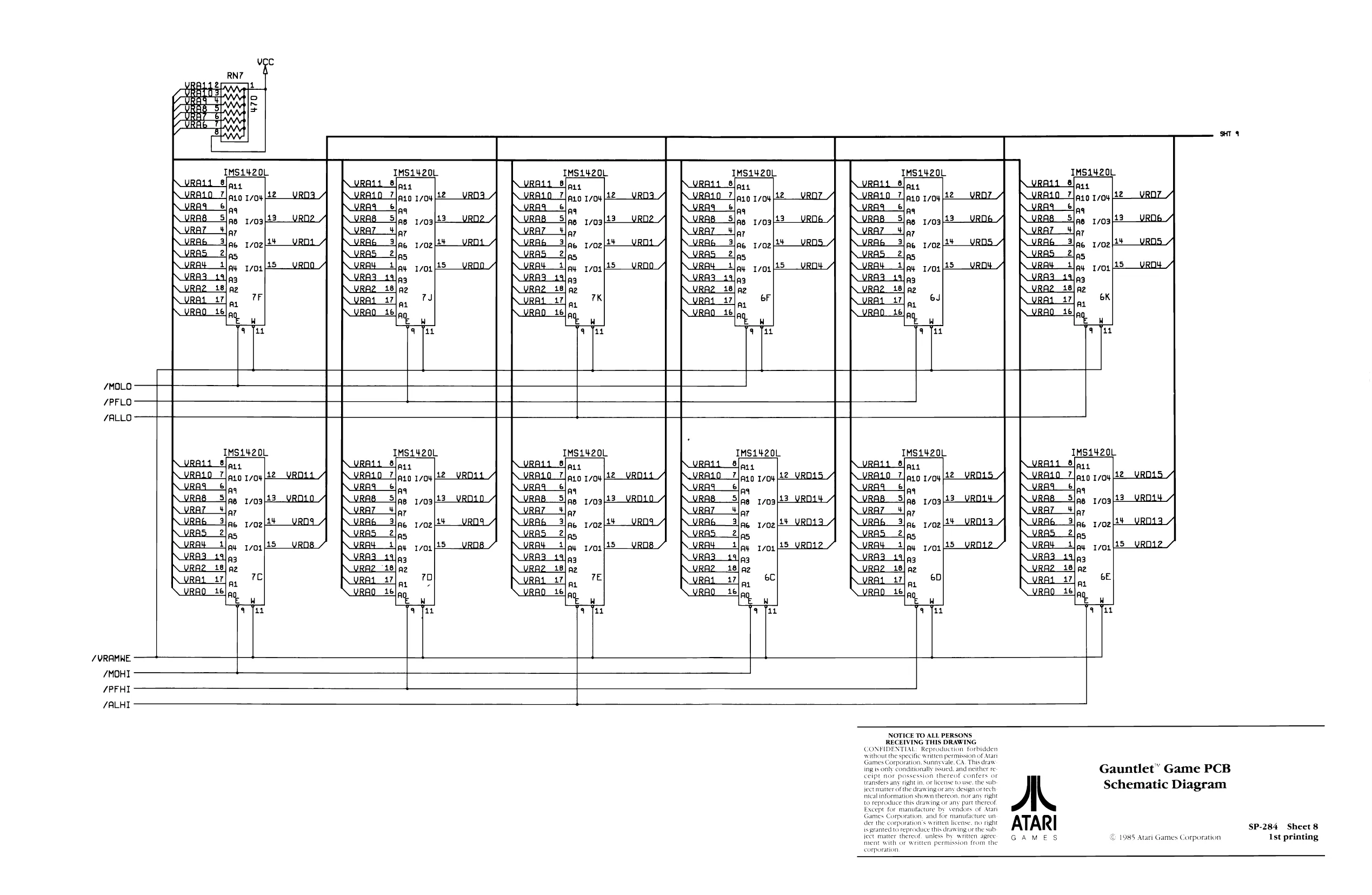
This page is a drawing, shown as the original scan.
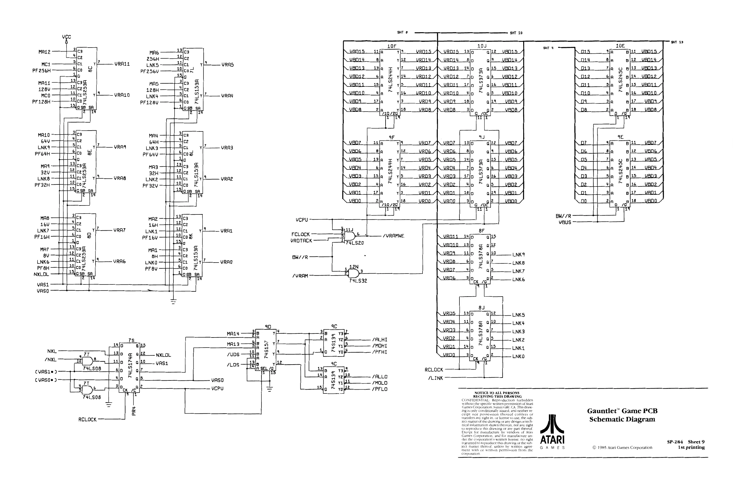
This page is a drawing, shown as the original scan.
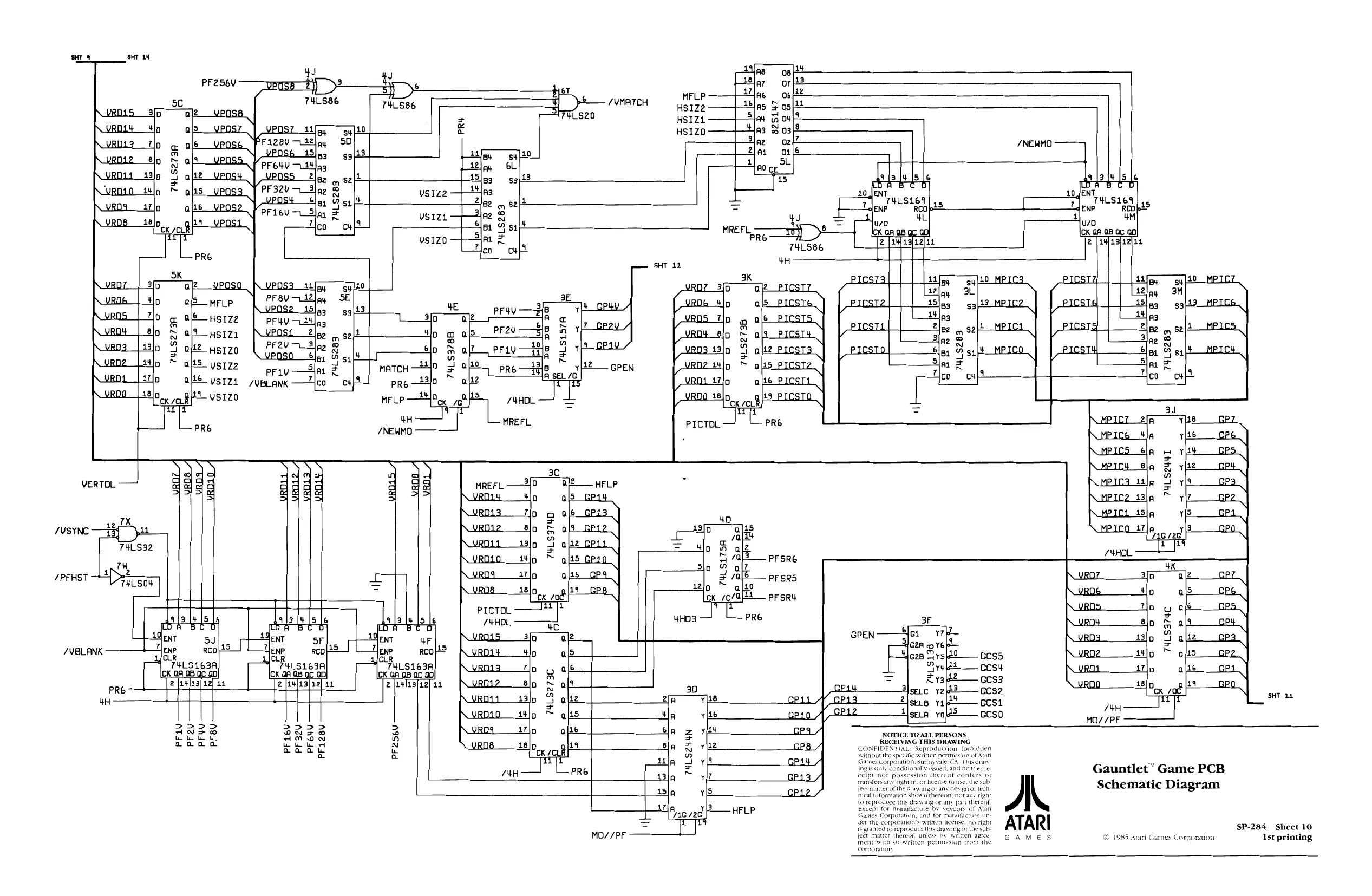
This page is a drawing, shown as the original scan.
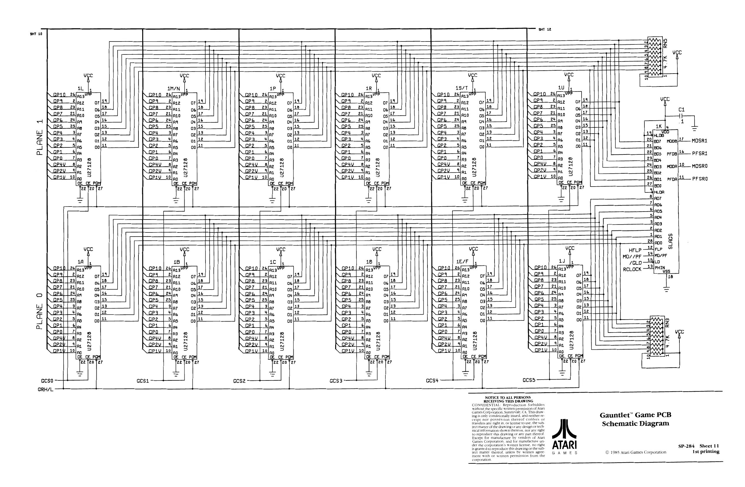
This page is a drawing, shown as the original scan.
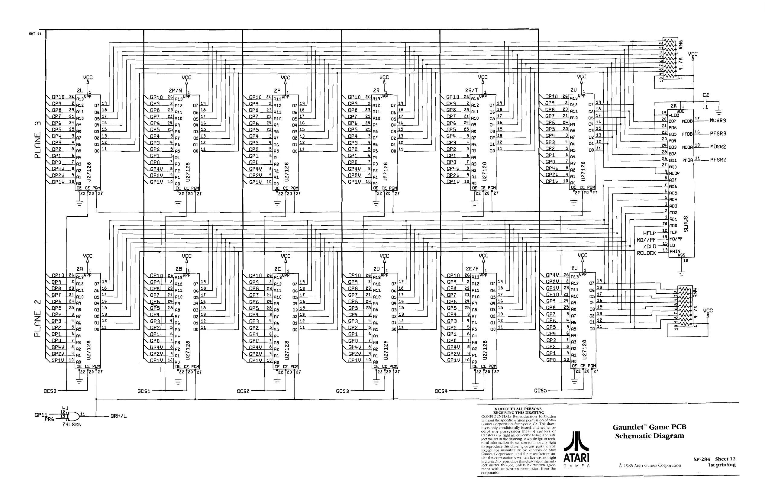
This page is a drawing, shown as the original scan.
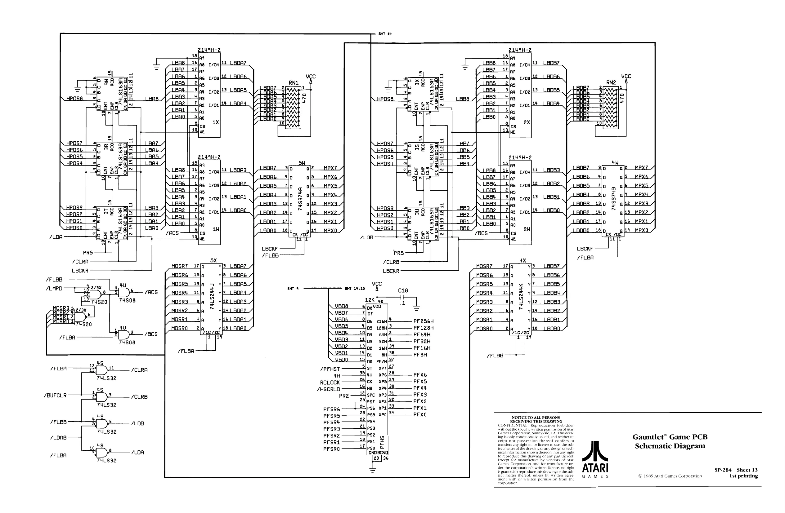
This page is a drawing, shown as the original scan.
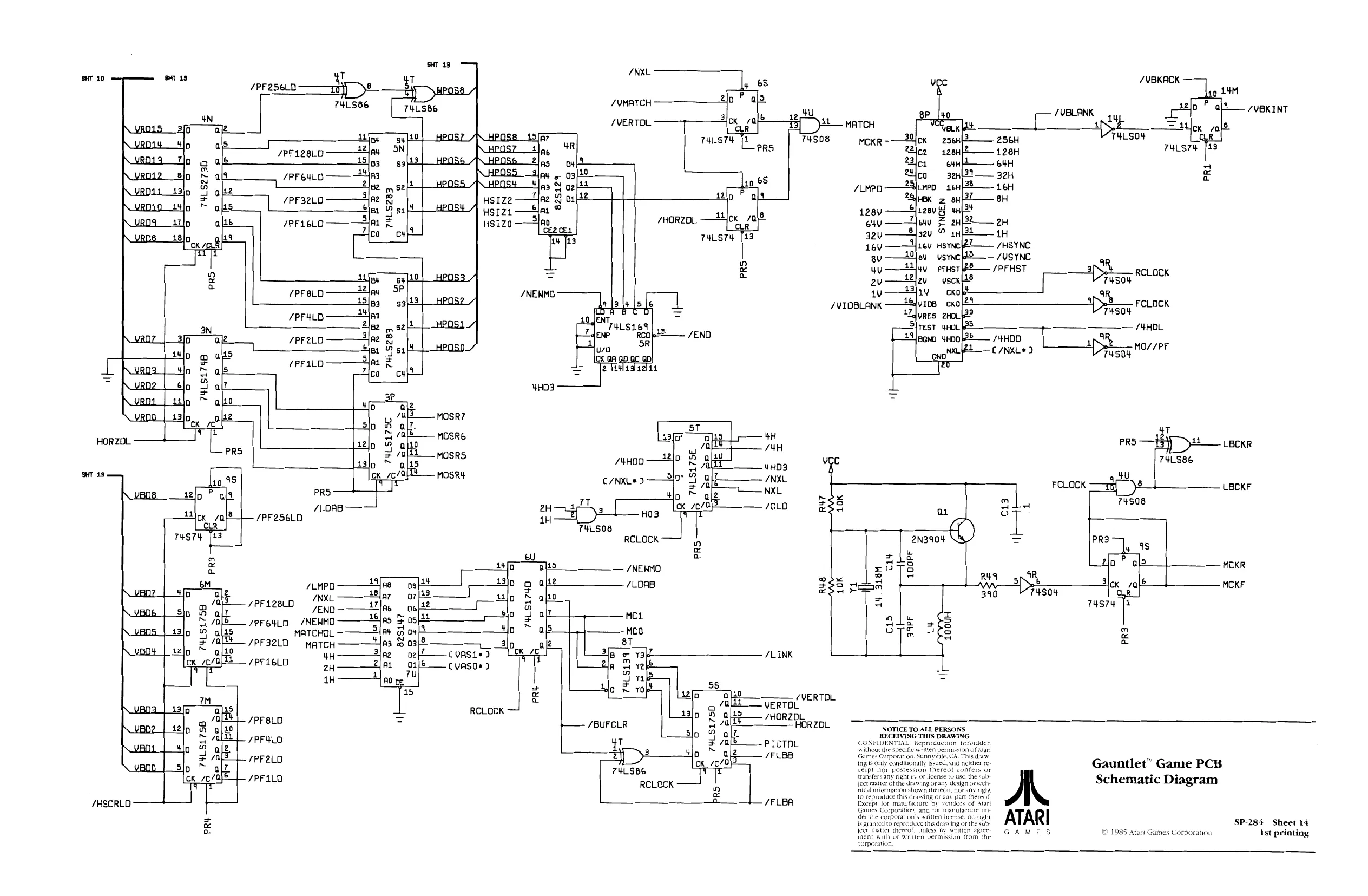
This page is a drawing, shown as the original scan.
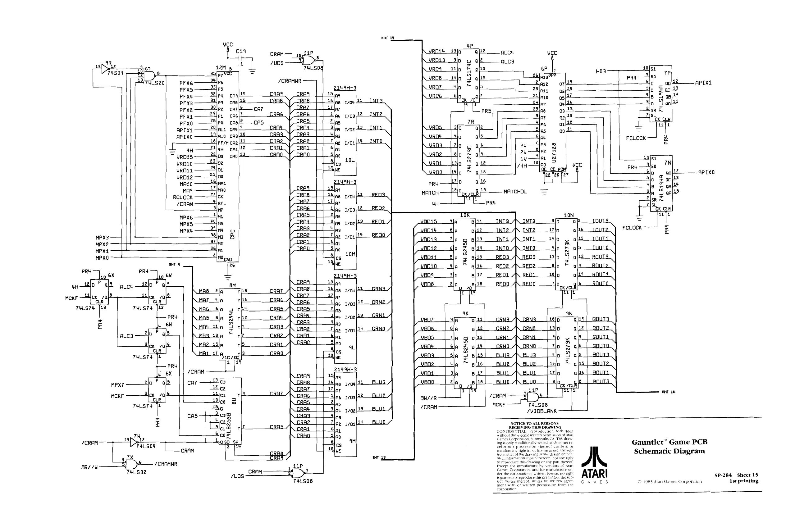
This page is a drawing, shown as the original scan.
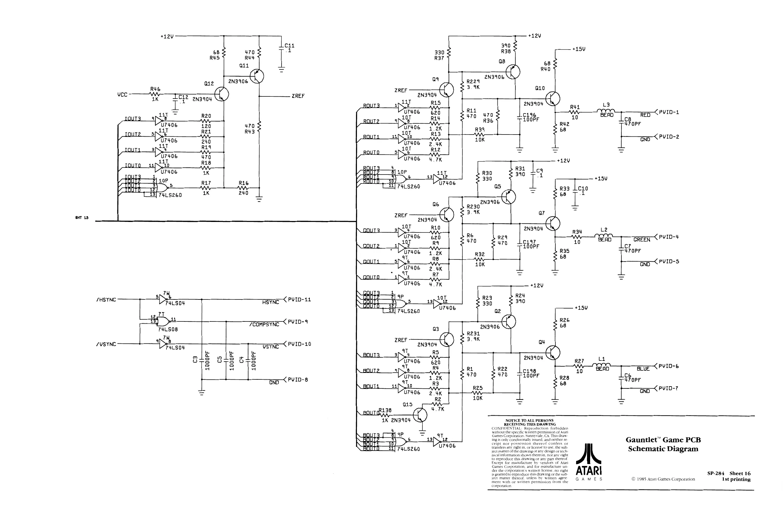
This page is a drawing, shown as the original scan.
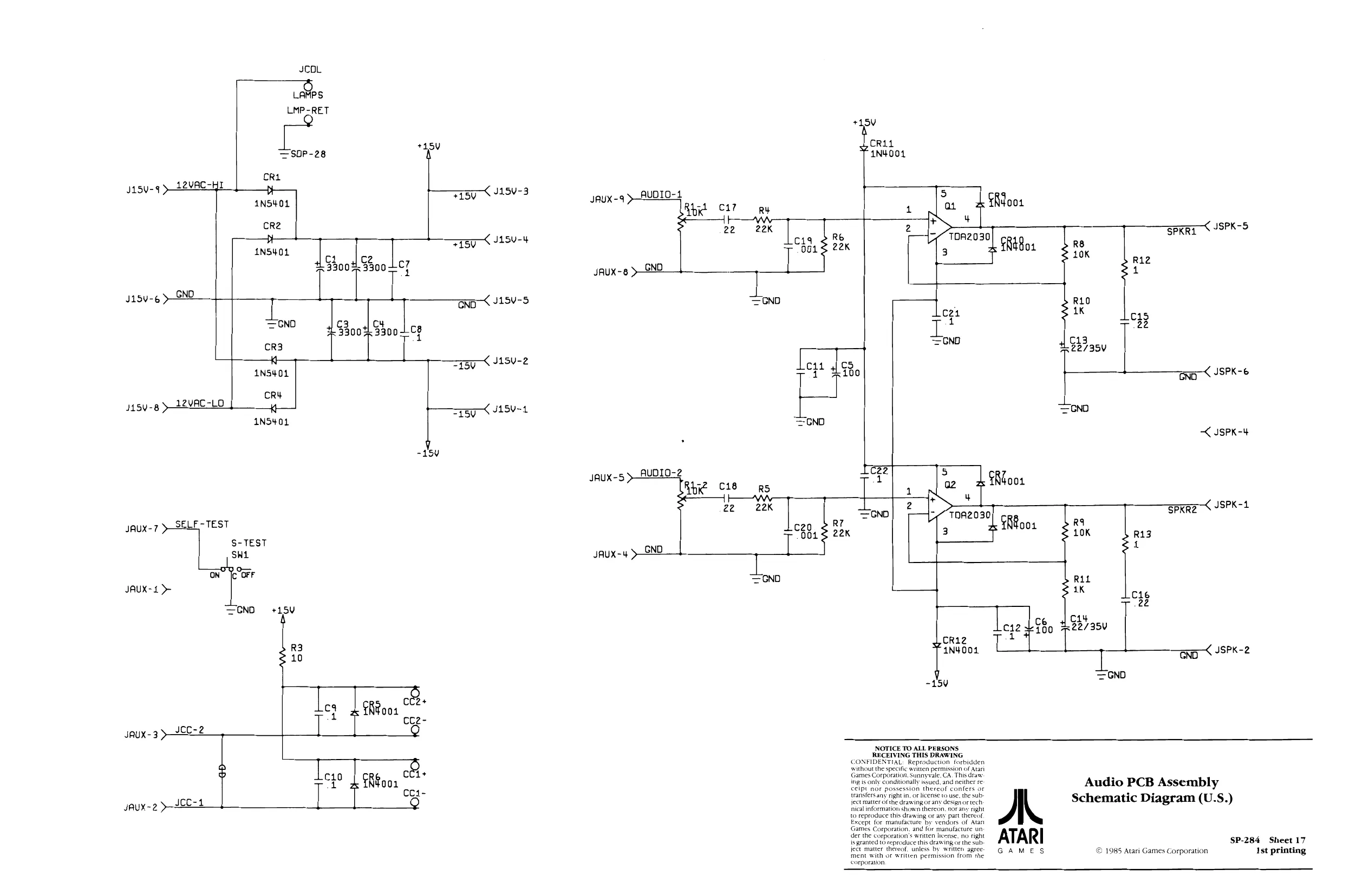
This page is a drawing, shown as the original scan.
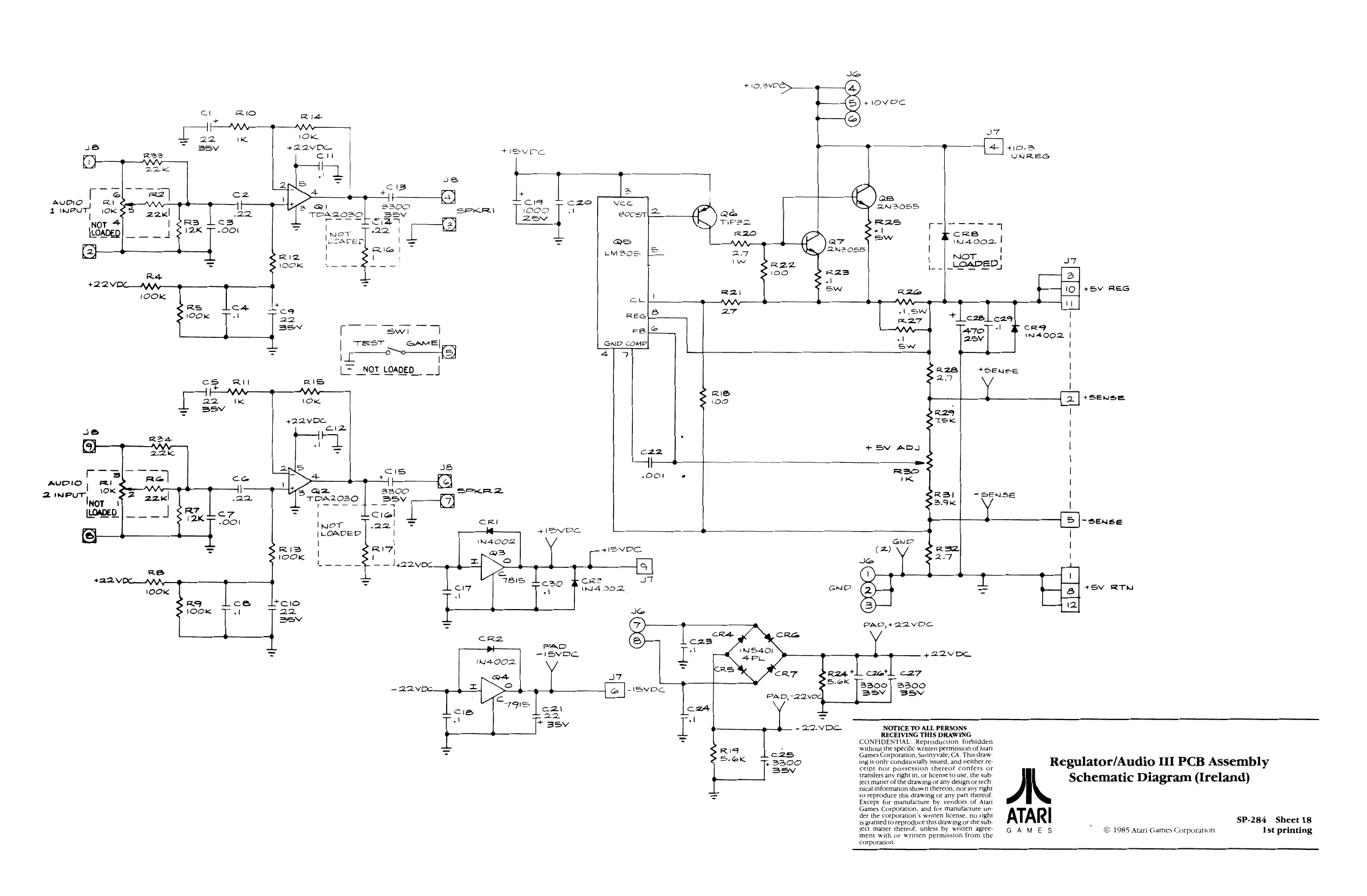
This page is a drawing, shown as the original scan.
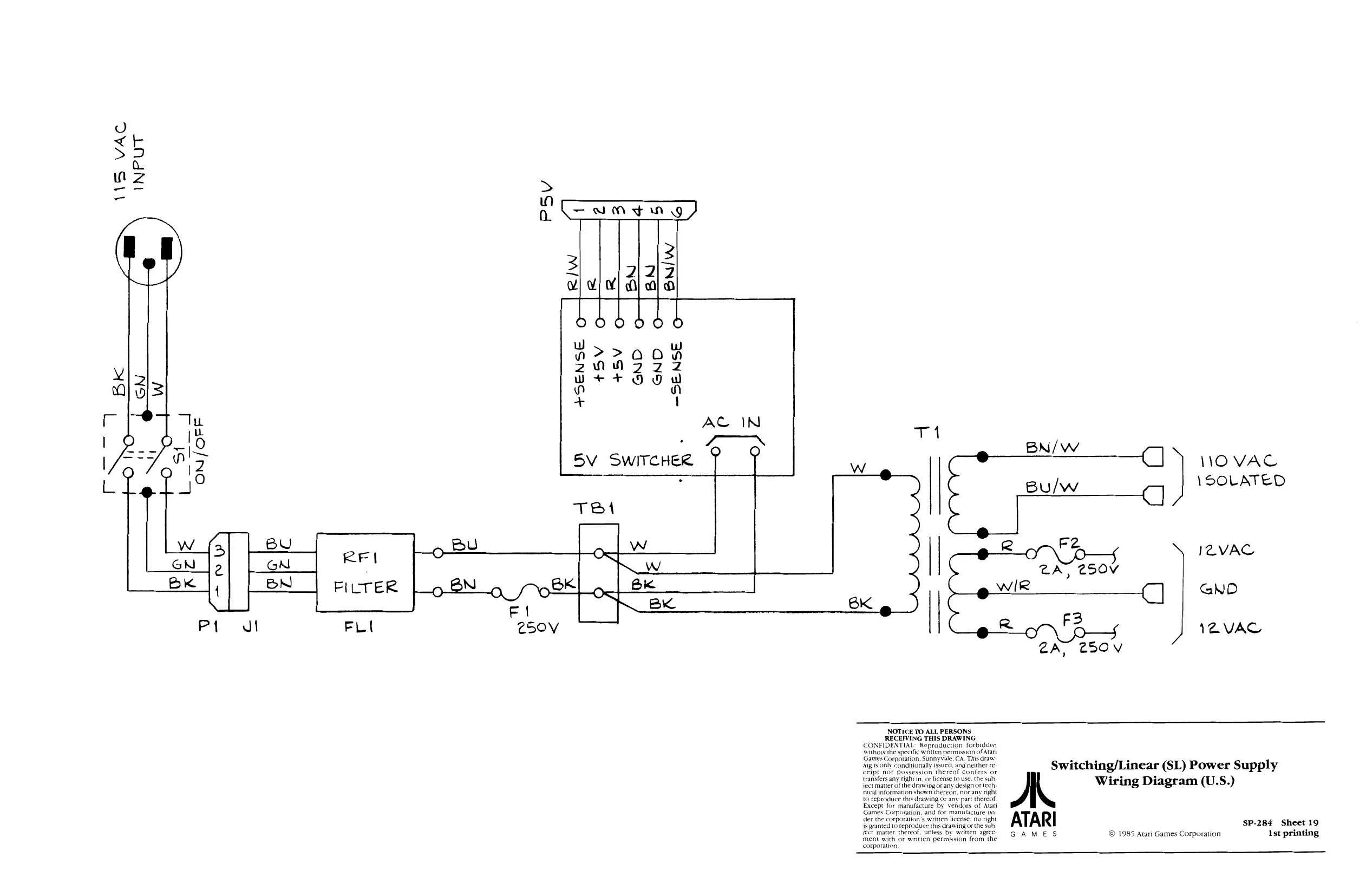
This page is a drawing, shown as the original scan.
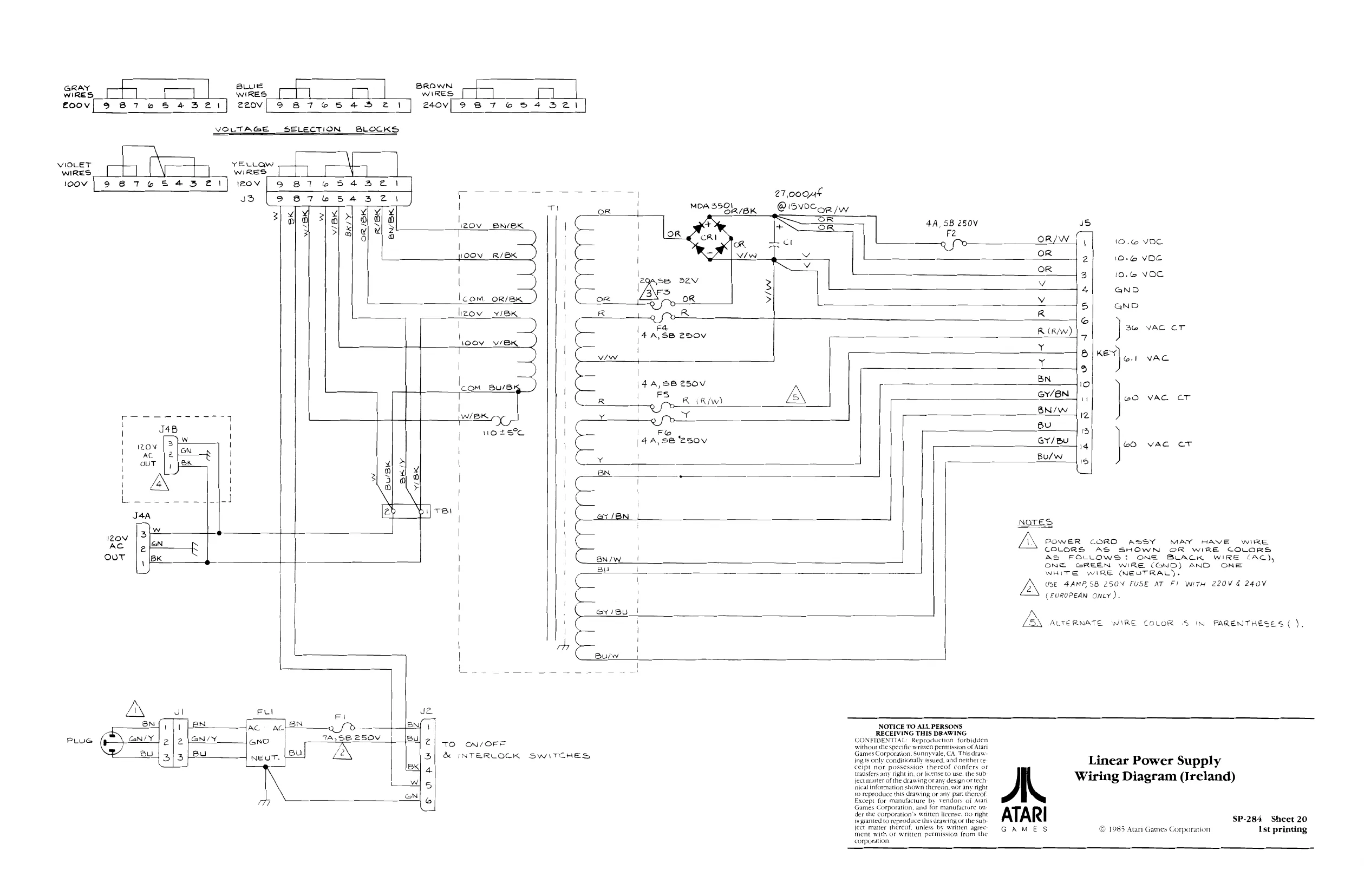
This page is a drawing, shown as the original scan.
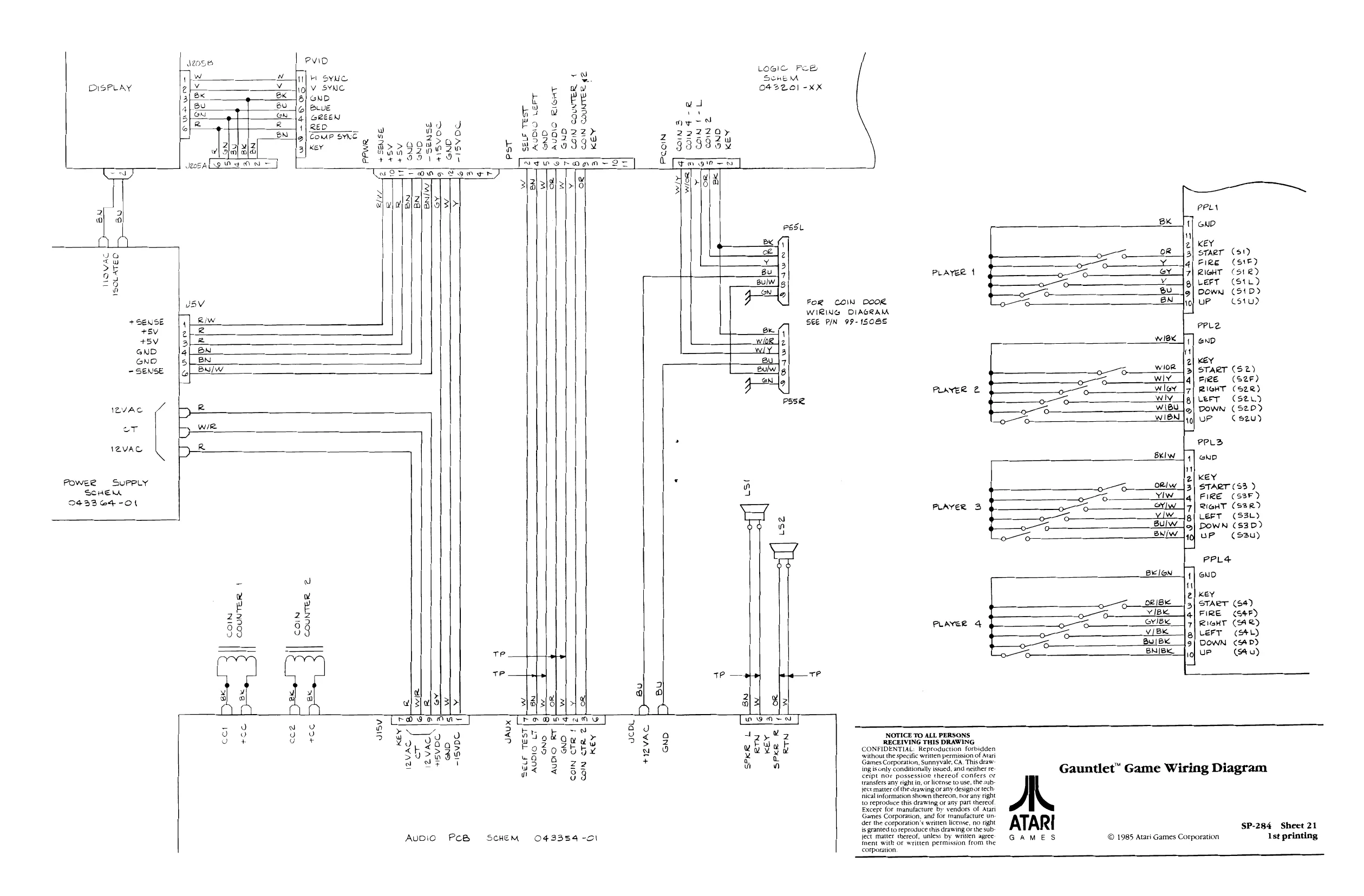
This page is a drawing, shown as the original scan.
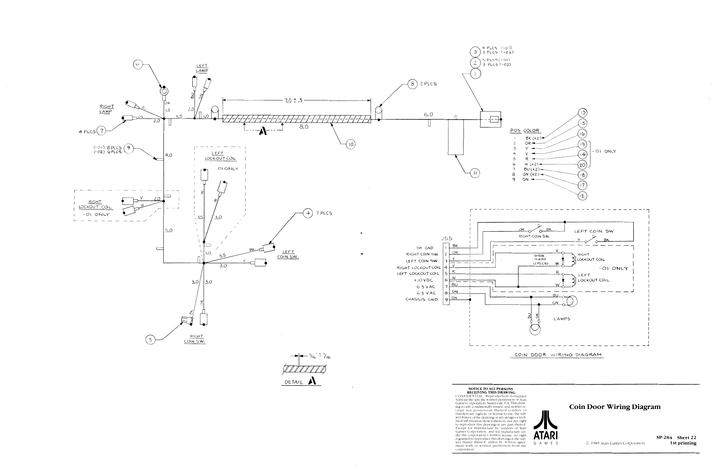
This page is a drawing, shown as the original scan.
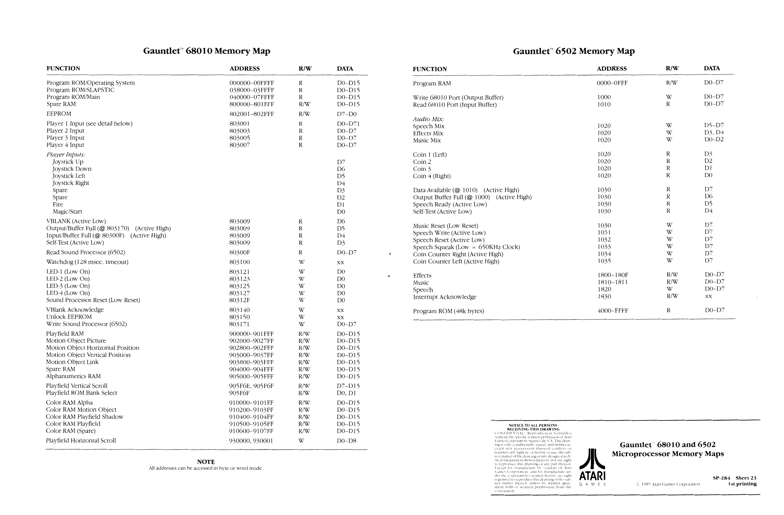
Gauntlet” 68010 Memory Map Gauntlet" 6502 Memory Map
| FUNCTION | ADDRESS | R/W | DATA | |
| Program ROM/Operating System | 000000-OOFFFF | R | DO-D15 | |
| Program ROM/SLAPSTIC | 038000 | FFF | R | DO-D15 |
| Program ROM/Main | 040000-07 | FFFF | R | DO-DI15 |
| Spare RAM | 800000-801FFF | RW | DO-DB15 | |
| EEPROM | 802001-802FFF | RW | D7-DO | |
| Player 1 Input (see detail below) | 803001 | R | DO-D71 | |
| Player 2 Input | 803003 | R | DO-D7 | |
| Player 3 Input | 803005 | R | DO-D7 | |
| Player | 4 Input | 803007 | R | DO-D7 |
Player inputs. Joystick Up D7 Joystick Down. D6 ick Left DS ick Right D4 D3 D2 DL Magic/Start DO
| VBLANK (Active Low) | 803009 | R | DO | |
| OutpuuBuffer Full (@ 803170) | (Active High) | 803009 | R | DS |
| Input/Buffer Full (@ 80300F) | (Active High) | 803009 | R | D4 |
| Self-Test (Active Low) | 803009 | R | D3 | |
| Read Sound Processor (6502) | 80300F | R | DO-D7 | |
| Watchdog (128 msec. timeout) | 803100 | w | XX | |
| LED-1 (Low On) | 803121 | w | Do | |
| LED-2 (Low On) | 803123 | w | DO | |
| LED-3 | (Low On) | 803125 | Ww | DO |
| LED-4 (Low On) | 803127 | Ww | DO | |
| Sound Processor Reset (Low Reset) | 80312F | Ww | DO | |
| VBlank Acknowledge | 803140 | Ww | XX | |
| Unlock EEPROM | 803150 | Ww | xx | |
| Write Sound Processor (6502) | 803171 | Ww | DO-D7 | |
| Playfield RAM | 900000-901 FFF | RW | DO-D15 | |
| Motion Object Picture | 902000-9027FF | RW | DO-D15 | |
| Motion Object Horizontal Position | 902800-902 FFF | RW | DO-D15 | |
| Motion Object Vertical Position, | 903000-9037FF | RW | DO-D15 | |
| Motion Object Link | 903800-903 FFF | RW | DO-D15 | |
| Spare RAM | 904000-904FFF | RW | DO-D15 | |
| Alphanumerics RAM. | 905000-905 FFF | RW | DO-DI5 | |
| Playfield Vertical Scroll | 905FGE, 905FOF | Rw | D7-D15 | |
| Playfield ROM Bank Select | 905F6F | RW | Do, D1 | |
| Color RAM Alpha | 910000-9101FF | RW | DO-DI5S | |
| Color RAM Motion Object | 910200-9103FF | RW | DO-D15 | |
| Color RAM Playfield Shadow | 910400-9104FF | RW | DO-D15 | |
| Color RAM Playfield | 910500-9105FF | RW | DO-D15 | |
| Color RAM (Spare) | 910600-9107FF | RAW | DO-Di5 | |
| Playfield Horizontal Scroll | 930000, 930001 | Ww | DO-D8 | |
| ADDRESS | RW | DATA | ||
| 0000-OFFF | RW | DO-D7 | ||
| Write 68010 Port (Output Buffer) | 1000 | Ww | DO-D7 | |
| Read 68010 Port (Input Buffer) | 1010 | R | DO-D7 | |
| 1020 | Ww | D5-D7 | ||
| 1020 | Ww | D3, D4 | ||
| 1020 | Ww | DO-D2 | ||
| 1020 | R | D3 | ||
| 1020 | R | D2 | ||
| 1020 | R | DI | ||
| 1020 | R | DO | ||
| Data Available (@ 1010) | (Active High) | 1030 | R | D7 |
| Output Buffer Full (@ 1000) | (Active High) | 1030 | R | D6 |
| Speech Ready (Active Low) | 1030 | R | DS | |
| Self-Test (Active Low) | 1030 | R | D4 | |
| Music Reset (Low Reset) | 1030 | Ww | D7 | |
| Speech Write (Active Low) | 1031 | Ww | D7 | |
| Speech Reset (Active Low) | 1032 | Ww | D7 | |
| Speech Squeak (Low = 650KHz Clock) | 1033, | w | D7 | |
| Coin Counter Right (Active High) | 1034 | Ww | D7 | |
| Coin Counter Left (Active High) | 1035 | WwW | D7 | |
| 1800-180F | RW | DO-D7 | ||
| 1810-1811 | RW | DO-D7 | ||
| 1820 | w | DO0-D7 | ||
| Interrupt Acknowledge | 1830 | RW | xx | |
| Program ROM (48k bytes) | 4000-FFFF | R | DO-D7 |
ment with « Corporatien NOTICE TO ALL PERSONS ® ING THIS DRAWING
GAMES € 1985 Atari Games Corporation Gauntlet” 68010 and 6502 Microprocessor Memory Maps
Ist printing
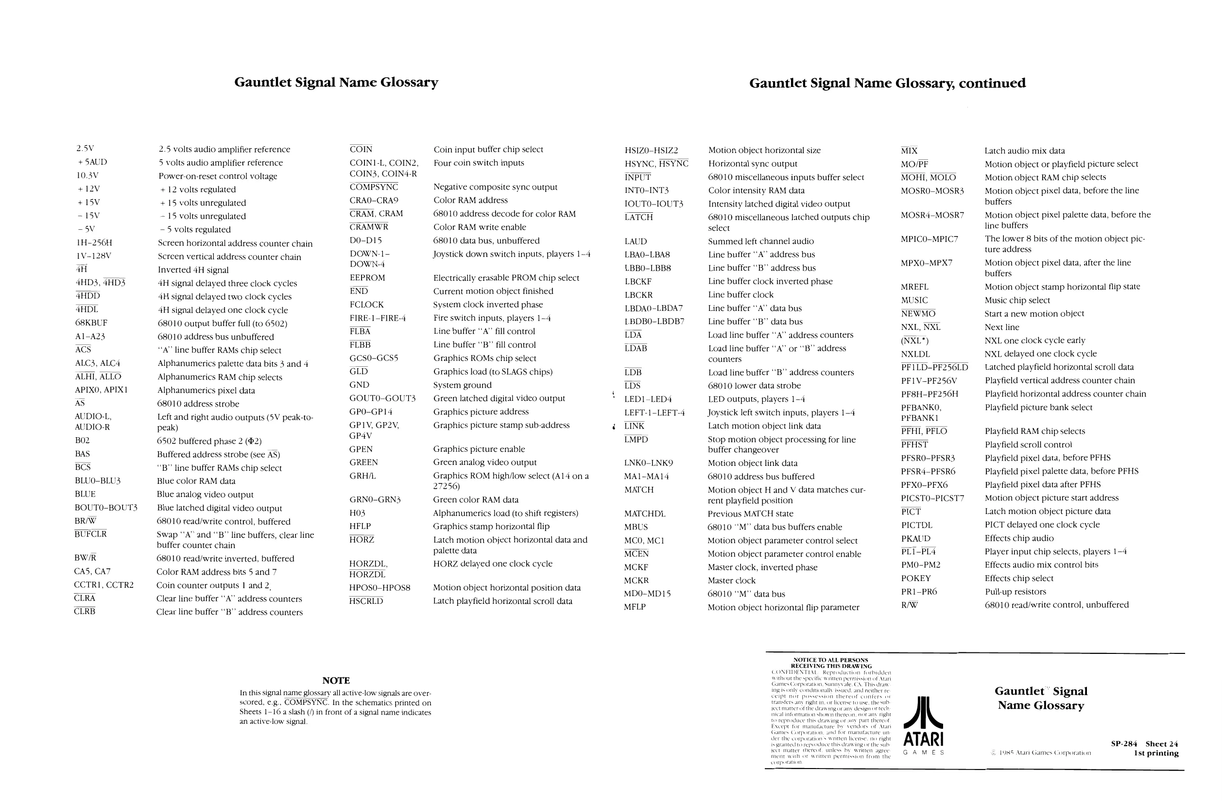
2.5V
+5AUD
10.3V
+12V
+15V
-15V
-5V
1H-256H
1V-128V 4H 4HD3, 4HD3 4HDD 4HDL 68KBUF
AI-A23 ACS
ALC3, ALC4 ALHI, ALLO APIXO, APIX1 AS
AUDIO-L, AUDIO-R
BO2
BAS
BCS
BLUO-BLU3 BLUE
BOUT
BRWW BUFCLR: -BOUT3
BWIR
CAS, CAT CCTRI, CCTR2 CLRA CLRB
Gauntlet Signal Name Glossary
2.5 volts audio amplifier reference 5 volts audio amplifier reference Power-on-reset control voltage + 12 volts regulated +15 volts unregulated ~ 15 volts unregulated ~5 volts regulated Screen horizontal address counter chain
Screen vertical address counter chain
Inverted 4H signal 4H signal delayed three clock cycles 4H signal delayed two clock les
4H signal delayed one clock cycle 68010 output buffer full (to 6502) 68010 address bus unbuffered “A” line buffer RAMs chip select Alphanumeric palette data bits 3 and 4 Alphanumerics RAM chip selects Alphanumerics pixel data 68010 address strobe
Left and right audio outputs (5V peak-topeak) 6502 buffered phase 2 (2) Buffered address strobe (see AS) “B" line buffer RAMs chip select Blue color RAM data
Blue analog video output Bive latched digital video output 68010 read/write control, buffered
Swap “A” and “‘B” line buffers, clear line buffer counter chain 68010 read/write inverted, buffered
Color RAM address bits 5 and 7
Coin counter outputs 1 and 2, Clear line buffer “A” address counters Clear line buffer ““B” address counters
In this signal name glossary all active-lo\ COIN
COINI-L, COIN2,
COMPSYNC,
CRAO-CRA9
CRAM, CRAM
EEPROM END
FCLOCK
FIRE-1-FIRE-4 FLBA FLBB
GCS0-GCSS GLD
GND
GOUT0-GOUT3
GPO-GP14
GP1V, GP2V, GP4
GREEN
GRH/L
GRNO-GRN3
HO3
HELP HORZ
HORZDL, HORZDL
HPOSO-HPOS8
HSCRLD
Negative composite sync output Color RAM address 68010 address decode for color RAM
Color RAM write enable
68010 data bus, unbuffered Joystick down switch inputs, players 1-4
Electrically erasable PROM chip select Current motion object finished System clock inverted phase Fire switch inputs, players 1-4 Line buffer “A” fill control
Line buffer ““B” fill control
Graphics ROMs chip select Graphics load (to SLAGS chips) System ground Green latched digital video output Graphics picture address Graphics picture stamp sub-address
Graphics picture enable Green analog video output Graphics ROM high/low select (A14 on a 27256) Green color RAM data
Alphanumerics load (to shift registers) Graphics stamp horizontal flip Latch motion object horizontal data and palette data HORZ delayed one clock cycle
Motion object horizontal position data Latch playfield horizontal scroll data HSIZO-HSIZ2
HSYNC, HSYNC INPUT
INTO-INT3
IOUTO-IOUT3 LATCH
LAUD.
LBAO-LBA8
LBBO-LBB8:
LBCKF
LBCKR
LBDAO-LBDA7
LBDBO-LBDB7 LDA LDAB
LDB TDS
LED1-LED4
LEFT-1-LEFT-4 LINK
LMPD
LNKO-LNK9
MAI-MAI14
MATCH.
MATCHDL
MBUS
MCO, MCL
MCE}
MCKF
MCKR
MDO-MD15
MFLP
Gauntlet Signal Name Glossary, continued
Motion object horizontal size Horizontal sync output 68010 miscellaneous inputs buffer select
Color intensity RAM data Intensity latched digital video output 68010 miscellaneous latched outputs chip select Summed left channel audio
Line buffer “A” address bus
Line buffer “B" address bus
Line buffer clock inverted phase Line buffer clock
Line buffer ‘‘A”’ data bus
Line buffer ‘“B” data bus
Load line buffer ‘A’ address counters
Load line buffer ‘A’ or “B” address. counters
Load line buffer ‘‘B’ address counters.
68010 lower data strobe LED outputs, players 1-4 Joystick left switch inputs, players 1-4 Latch motion object link data Stop motion object processing for line buffer changeover Motion object link data 68010 address bus buffered
Motion object H and V data matches current playfield position Previous MATCH state
68010 “‘M” data bus buffers enable Motion object parameter control select Motion object parameter control enable Master clock, inverted phase Master clock
68010 *M” data bus
Motion object horizontal flip parameter MIX MO/PF
MOHI, MOLO.
MOSRO-MOSR3
MOSR4—MOSR7
MPICO-MPIC7
MPXO-MPX7
MREFL.
MUSIC NEWMO
NXL, NXL (NXL*) NXLDL PFILD-PF256LD
PF1V-PF256V PF8H-PF256H
PFBANKO, PFBANK1 PFHI, PFLO PFHST.
PFSRO-PFSR3
PESR4—-PFSRO
PEX0-PFX6
PICSTO-PICST7
PICT
PICTDL
PKAUD PLI-PL4
PMO-PM2
POKEY PRI-PRO
RW Latch audio mix data Motion object or playfield picture select Motion object RAM chip selects Motion object pixel data, before the line buffers
Motion object pixel palette data, before the line buffers
The lower 8 bits of the motion object picture address
Motion object pixel data, after the line buffers
Motion object stamp horizontal flip state Music chip select Start a new motion object Next line NXL one clock cycle early NXL delayed one clock cycle Latched playfield horizontal scroll data Playfield vertical address counter chain Playfield horizontal address counter chain. Playfield picture bank select
Playfield RAM chip selects Playfield scroll control Playfield pixel data, before PFHS Playfield pixel palette data, before PFHS Playfield pixel data after PFHS Motion object picture start address Latch motion object picture data PICT delayed one clock cycle Effects chip audio Player input chip selects, players 1-4 Effects audio mix control bits
Effects chip select Pull-up resistors 68010 read/write control, unbuffered
NOTICE TO AUL PERSONS
RECEIVING THIS DRAWING
CONFIDENTIAL Reproduction forbidden, without the specific written pers wxtarh Games Corporation, Sunnyvale. CS. Thisdraw ing is only conditionally issued. hdl neither te CeipL nor possession thereol coanters er transfers any right mor license 19 use, the sub ect matter of the draw igor any clesgo oF tech fica information shown thereon. AbEaNy sight to reprodiice tl Except for manu drawing or ae part thereot ture by vendors of tari na! for MeanUactee s written license. ne right ue this drawing or the sub ject matter thereot. unless by waten agree ment with oF Weilten permission fron the corporation AL
ATARI
GAMES
Gauntlet” Signal Name Glossary
©. 19M5 Atari Games Corporation 1st printing
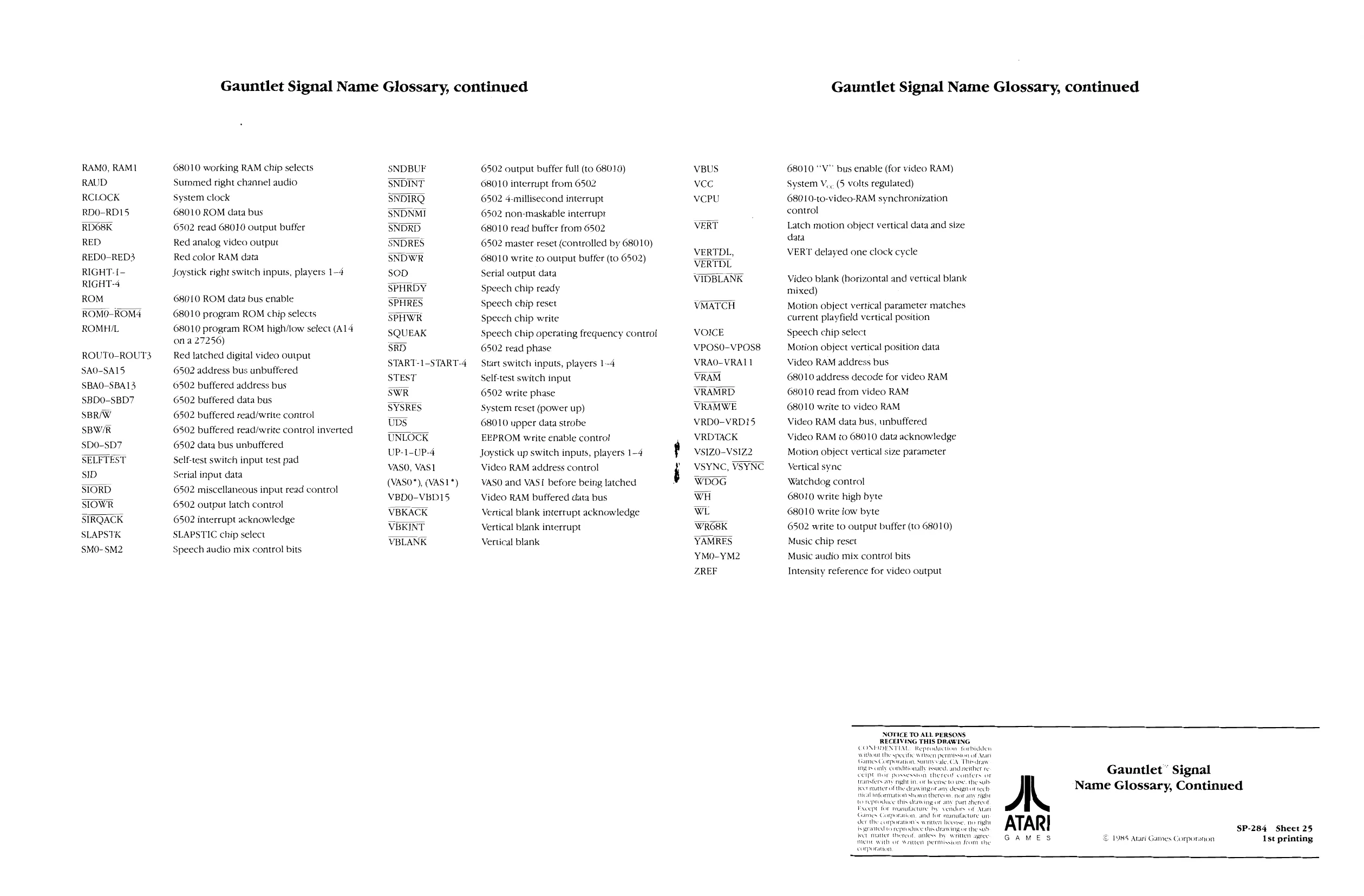
RAMO, RAM1 RAUD
RCLOCK RDO-RDI5 RDO8K
RED
REDO-RED3
ROMO-ROM4 ROMHIL
ROUTO-ROUT3 SAO-SA15 SBAO-SBA13,
SIRQACK SLAPSTK SMO-SM2
Gauntlet Signal Name Glossary, continued
68010 working RAM chip selects Summed right channel audio System clock 68010 ROM data bus 6502 read 68010 output buffer
Red analog video output Red color RAM data Joystick right switch inputs, players 1-4
68010 ROM data bus enable 68010 program ROM chip selects 68010 program ROM high/low select (A14 ona 27256) Red latched digital video output 6502 address bus unbuffered 0502 buffered address bus 6502 buffered data bus
6502 buffered read/write control 6502 buffered read/write control inverted 6502 data bus unbuffered Self-test switch input test pad Serial input data 6502 miscellaneous input read control 6502 output latch control 6502 interrupt acknowledge SLAPSTIC chip select Speech audio mix control bits SNDBUF INT DIRQ SNDNMI
SPHWR SQUEAK
START-1-START-4 STEST SWR
UNLOCK UP-1-UP-4
VASO, VASI (VASO*), (VAS1*) VBD0-VBD15 VBKACK VBKINT. 6502 output buffer full (to 68010) 68010 interrupt from 6502 6502 4-millisecond interrupt 6502 non-maskable interrupr 68010 read buffer from 6502 6502 master reset (controlled by 68010) 68010 write to output buffer (to 6502) Serial output data Speech chip ready Speech chip reset Speech chip write Speech chip operating frequency control 6502 read phase Start switch inputs, players 1-4 Self-test switch input 6502 write phase System reset (power up) 68010 upper data strobe EEPROM write enable contro! Joystick up switch inputs, players 1-4 Video RAM address control VASO and VASI before being latched Video RAM buffered data bus Vertical blank interrupt acknowledge Vertical blank interrupt Vertical blank VBUS vcc
VCPU
VERTDL, VERTDL VIDBLANK
VMATCH
VOICE VPOSO-VPOS8 VRAO-VRAI1 VRAM VRAMRD VRAMWE VRDO-VRDI5, VRDTACK VsIZ0-
WDOG WH WL WRO8K YAMRES YM0-YM2
ZREF
68010 “V" bus enable (for video RAM) stem V,, (5 volts regulated) 68010-to-video-RAM synchronization control Latch motion object vertical data and size data VERT delayed one clock cycle
Video blank (horizontal and vertical blank mixed) Motion object vertical parameter matches current playfield vertical position Speech chip select Motion object vertical position data Video RAM address bus 68010 address decode for video RAM 68010 read from video RAM 68010 write to video RAM Video RAM data bus, unbuffered Video RAM to 68010 data acknowledge Motion object vertical size parameter Vertical sync Watchdog control 68010 write high byte 68010 write iow byte 6502 write to output buffer (to 68010) Music chip reset Music audio mix contro! bits
Intensity reference for video output
NOTICE TO ALL PERSO
RECEIVING THIS DRA CONFIDENTIAL Reproduction forbidden without the specie Witten permission ot Mar Games Corporation, Sunny sale, CA."Thiveras ings only condtionally ssuled. and aeither re ceipt ter possesstan thereat canters OF transfers aay right in or ficense to se. the sub ject mater of the draveingor any design ar eecb tical formation shown thereon. nar any she to reprodce this deassing a anv part thercot Fxcept for musuficture by venders of Matt Games Corporation, and for manfactare an der the corporation's writhe License, ney Fight is granted eo reproduce diisdrawingor the sts iect matter thereof, ankess by written sere mene with oF Written permission Jeo the AN
ATARI
GAMES
Gauntlet” Signal Name Glossary, Continued
1985 Atari Games Corporition 1st printing