Popeye Operation Manual (TPP2-UP TPP2-UP-US)
Popeye (revision D) (Nintendo, 1982) · Manual · 42 pages · 18 sections · original scan
2P.C.BOARDS TYPE
© 1982 King Features Syndicate
OPERATION MANUAL
MODEL NO: TPP2-UP |
MODEL NO: TPP 2-UP-US
Nintendo’
This equipment generates, uses, and can radiate radio frequency energy, and if not installed and used in accordance with the instructions manual, may cause interference to radio communications. It has been tested and found to comply with the limits for a Class A computing device pursuant to Subpart J of Part 15 of FCC Rules, which are designed to provide reasonable protection against such interference when operated in a commercial environment. Operation of this equipment in a residential area is likely to cause interference in which case the user at his own expense will be required to take whatever measures may be required to correct the interference.
Use of non-Nintendo parts or modifications of your Nintendo game circuitry may adversely affect the safety of your game, and may cause injury to your players.
1 Contents [
- Maintenance and Repair -- . Location Setup A. Game Inspection ---- B. Game Installation ----
- Voltage Selection
- Power On/Off Switch ---
- Adjustment of VideO MONitor --.-eeeeeeeeeeeeeeeeeeee ee ee eens . Option Switch Settings A. Game Price Settings --- ween B. Game Option Settings ---.--eseceesseeeeeeeeseeee eset esse eeee neces « SOIF-TESt .----ccecceceeeene tec c sce ete eseeneceeeneneteeeeneeesseeseeennseseneeeneeees
A. Fuse Replacement °- B. Cleaning ---++-+-+++- Cc. Operation Panel ---- D. Video Monitor removal E. Game PCB removal
. Radio Frequency Interference --- » Wiring and Connection -----:rer:seereeeececer seers ener corer ennneseentrneee . Name of each part and Parts List ---++++-++--+1reereeeeeeteeeeee
- Location Setup
A. Game Inspection
POPEYE Display Panel
Game Serial Number Label POPEYE Front Screen
POPEYE
Operation Panel
Coin Door
Video Monitor
Game PCB ‘ Shield Cover: Shield Cage " Wie
Power Cord “Main Fuse Power Transformer
Power On/Off Switch:
Fig. | Game Overview
Check before plugging the game in !
The game “POPEYE” is shipped ready for operation, but a last visual check should be made to insure the final touch of quality control. Please check the following to help us insure that your new game was delivered to you in good condition.
- Check the exterior of the game for shipping damage, dents, chips, or broken parts.
- Remove the screws on the Rear Panel.
- Unlock and open the Rear Panel, as well as the Coin Door; inspect the interior of the game as follows:
- Check that Plug-in connectors are firmly connected.
- Check that Plug-in integrated circuits on the Game PCB are firmly connected in their sockets.
- Check that all major subassemblies such as the Power Supply, Operation Panel, and Video Monitor are properly mounted.
- Remove the tie-wrap that holds the coiled Power Cord on the inside cabinet wall. Check the cord for any cuts or dents in the insulation.
B. Game Installation
Fig. 2 Installation Requirements
Power : 101 watts Temperature : Oto 38deg.C (32 to 100 deg.F) Humidity : Not over 95% relative Space required: 60(W) < 85(D)cm (23 1/2 « 33 1/2 in.) Height : 170cm (67in.)
- Voltage Selection Before plugging in your game, make sure the Terminal Block of the Power Supply is correct for your location’s line voltage.
Power Supply Fuse
Terminal Block US. 90~120V Europe 200~240V
Outlet through Isolation Transformer AC 100V
Fig. 3 Power Supply and Voltage Selection
- Power On/Off Switch A Power On/Off Switch is located in the rear of the game at the bottom right side of the cabinet. See Fig. 1.
This game MUST be grounded. Failure to do so may result in destruction to electronic components.
If the results of the preceding steps are satisfactory, you are ready to plug the game in, and set the Power On/Off Switch to the “On” position.
- Adjustment of Video Monitor
From To Game PCB Green Gain Video Monitor 6P—600 Video Red Gain 4K Main PCB
Harness Blue Gain Signal PCB
INVERT OUT
In case of TPP—UP, Plug in here!
This Signal PCB is only attached to TPPU-20-00 :Video Monitor (32Type] 20-EZV(R-C),
SOUND VOLUME
—— H-HOLO ec
FUSE 4A, fo | Video Monitor
v Main PCB
FUSE 0.38
Fig. 4 Video Monitor
Do not touch the inside of the Video Monitor in which many parts are supplied with high voltage.
- Option Switch Settings
A pair of Option Toggle Switches are mounted on the Game PCB.
for Window
Toggle -switch
1 JK L MN OP
sw2
ABCD sw
Fig. 5 Option Toggle Switches
A. Game Price Settings You can set the game price multipliers with Toggles A thru D (SW1) on the Game PCB.
Fig. 6 Game Price Settings
Toggle Settings credit/coin
| A | B | Cc | D | |
| 1/3 | OFF | OFF | ON | ON |
| 1/2 | ON | OFF | OFF | OFF |
1/1 OFF | OFF | OFF | OFF
| 2/1 | OFF | ON | OFF | OFF |
| 3/1 | ON | OFF | ON | OFF | |
| 4 | OFF | ON | ON | OFF | |
| 5/1 | OFF | ON | OFF | ON |
| 6/1 | ON | ON | ON | OFF |
| Freeplay | ON | ON | ON | ON |
B. Game Option Settings
- Number of POPEYE per Game Set the number of POPEYE per game with Toggles | & J (SW2) on the Game PCB.
Fig. 7 Number of POPEYE per Game
Number of | Toggle Settings POPEYE
| per Game | | | J |
1 OFF | OFF
| 2 | ON | OFF | |
| $ | 3 | OFF | ON |
| 4 | ON | ON |
$: factory settings
- Game Difficulty Set the game difficul
Fig. 8 Game Difficulty
Game Toggle Settings
Difficulty K L
| Easy (0) | OFF | OFF |
| (1) | ON | OFF |
| (2) | OFF | ON |
| Hard (3) | ON | ON |
y with Toggles K & L (SW2) on the Game PCB.
- Bonus POPEYE Set the Points for bonus POPEYE with Toggles M&N (SW2) on the Game PCB.
Fig. 9 Bonus POPEYE
Bonus Toggle Settings POPEYE
| at | M | N |
| 40,000pts. (0) | OFF | OFF |
| 60,000pts. (1) | ON | OFF |
| 80,000pts. (2) | OFF | ON |
| No Bonus (3) | ON | ON |
- Attract Music It is a new feature to play the theme music “POPEYE” on the game Attract Mode. You can select “With music” or “Silent” with Toggle O (SW2) on the Game PCB.
Fig. 10 Attract Music
Attract Toggle Setting
Music O
Silent (0) Orr. $ | With music (1) ON $: factory setting
- Upright/Table Version Select
Fig. I1 Upright/Table
Toggle Setting Version P
Table (0) OFF $] Upright (1) ON $: factory setting
All the Option Switch Settings MUST be done with Power Off.
- Self-Test
A. Self-Test Menu
- Entry With pressing Service Switch, set the Power On/Off Switch to the “On” position.
- Audio Test You will hear a beep sound.
- RAM Test The result of RAM Test will be displayed on the Video Monitor as follows. Example
RAM location RAM TEST on the PCB | —— 7H NG ————_—_—_ Failed (CPU PCB)
- ROM Test The result of ROM Test will be displayed on the Video Monitor as follows. Example
ROM location ROM TEST on the PCB = ————®- 7A OK (CPU PCB) 7B OK ~#———-—_ Passed 7C OK 7E NG ~<—_—_—_—_ _ Failed
- Option Switch Test The Toggle Settings will be displayed on the Video Monitor as follows.
Example
OPTION SWITCH A B Cc D See Fig. 6 ——*™ COIN OFF OFF OFF OFF
POPEYE 3 —-—————— See Fig. 7 See Fig. 8 ——* DIFFICULTY 2 BONUS 1 ——_——_—_ See Fig. 9 See Fig. 10 ——* MUSIC 1 VERSION 1 | 4 Fig. 14
- Press any switch on the Operation Panel in order to step to next test !!
- Switch Test You will hear a beep sound for each press of the switches; 4 way Controller, Punch Switch, 1-Player Switch, 2-Player Switch, Service Switch, and Coin Switch.
- The end of Self-Test.
- Maintenance and Repair
A. Fuse Replacement This game contains 4 fuses. Replace fuses only with the same type as listed below.
Fig. 12 Specification of Fuses
- Main fuse U.S. : 4A 100V ( 90~120V) Europe : 2A 250V (200~ 240V) See Fig. 1
- Power Supply fuse 3A 100V See Fig. 3
- Video Monitor fuse 4A 100V | 0.3A 100V See Fig. 4
B. Cleaning The exterior of the game, all metal parts and all plastic parts can be cleaned with a nonabrasive cleanser. You have to be careful when cleaning the glass or plastic parts. A dry cloth may cause scratches and results in a foggy appearance.
C. Operation Panel
- Operation Panel removal Before repairing or replacing any switch or 4 way Controller on the Operation Panel, unplug the game. Then open the Coin Door. Reach through the Coin Door opening and unlock the Clamps, located at each end on the underside of the Operation Panel. See Fig. 16.
- Micro-switch Replacement Whenever you replace any micro-switch on the Operation Panel, a switch gap adjustment is needed as shown in Fig. 13, and
See Fig. 22.
Press
Switch Button Ass'y
Gap:0.2~0.5 mm (1/128 ~ 5/256 inch)
Fig. 13 Switch gap adjustment
- Lubrication for 4 way Controller To maintain the 4 way Controller in good condition, lubricate the pillow balls and 4 way Guide Plate approx. every 3 months. See Fig. 14.
Fig. 14 Lubrication points
D. Video Monitor removal
- Front Screen removal Unlock and open the rear panel, pull the Front Screen Clamp. Lift the Front Screen upward while pushing and then pull toward you. See Fig. 15 & Fig. 16.
Front Screen Clamp
Operation Panel
Clamp
Fig. 16 Front Screen and Coin Door Operation Panel removal
- Video Monitor removal lf you need to remove the Video Monitor, follow the instructions listed below. But the following procedure should only be performed by an experienced service technician.
It is recommended the game be left unplugged for at least one hour before removing the Video Monitor. This will probably discharge the CRT, but extreme caution is still necessary.
- Check the game is unplugged !!
- Open the rear panel and remove the Front Screen.
- Unplug all the harness and cables from the Video Monitor.
- Standing at the front opening of the game, remove the four mounting bolts and flat washers. See Fig. 17.
- From the rear opening, carefully lift the Video Monitor and pull toward you.
Use extreme causion and do not touch electrical parts of the yoke area with your hands or with any metal object in your hands.
Remove the four mounting bolts and flat washers
Fig. 17 Video Monitor removal
—E. Game PCB removal
- Check the game is unplugged !!
- Open the rear panel.
- Remove the 44-pin edge connector from the upper side of the 031-FCC PCB on the Shield Cover.
- Locate the 6 Phillips-head Screws on the Shield Cover. Remove and save these Screws.
- Remove the Game PCB from the Shield Cage by carefully sliding it straight out of the wooden PCB retainer.
A reversed connector will damage your PCB! If the connectors don’t slip on easily, don’t force them !
031-FCC PCB
6 Phillips-head Screws a ° stata Cage
Shield Cover
Fig. 18 Game PCB removal
5. Radio Frequency Interference (RFI)
In order to keep protecting against the RFI radiated from this equipment, please read the following attentions.
- Do not use non-Nintendo parts !
- Do not modify your game circuitry !
- Do not modify the wiring harness and connections !
- Connect this game only to a grounded 3-wire outlet.
- After servicing the Game PCB, shut the Shield Cover completely by the Screws. See Fig. 18.
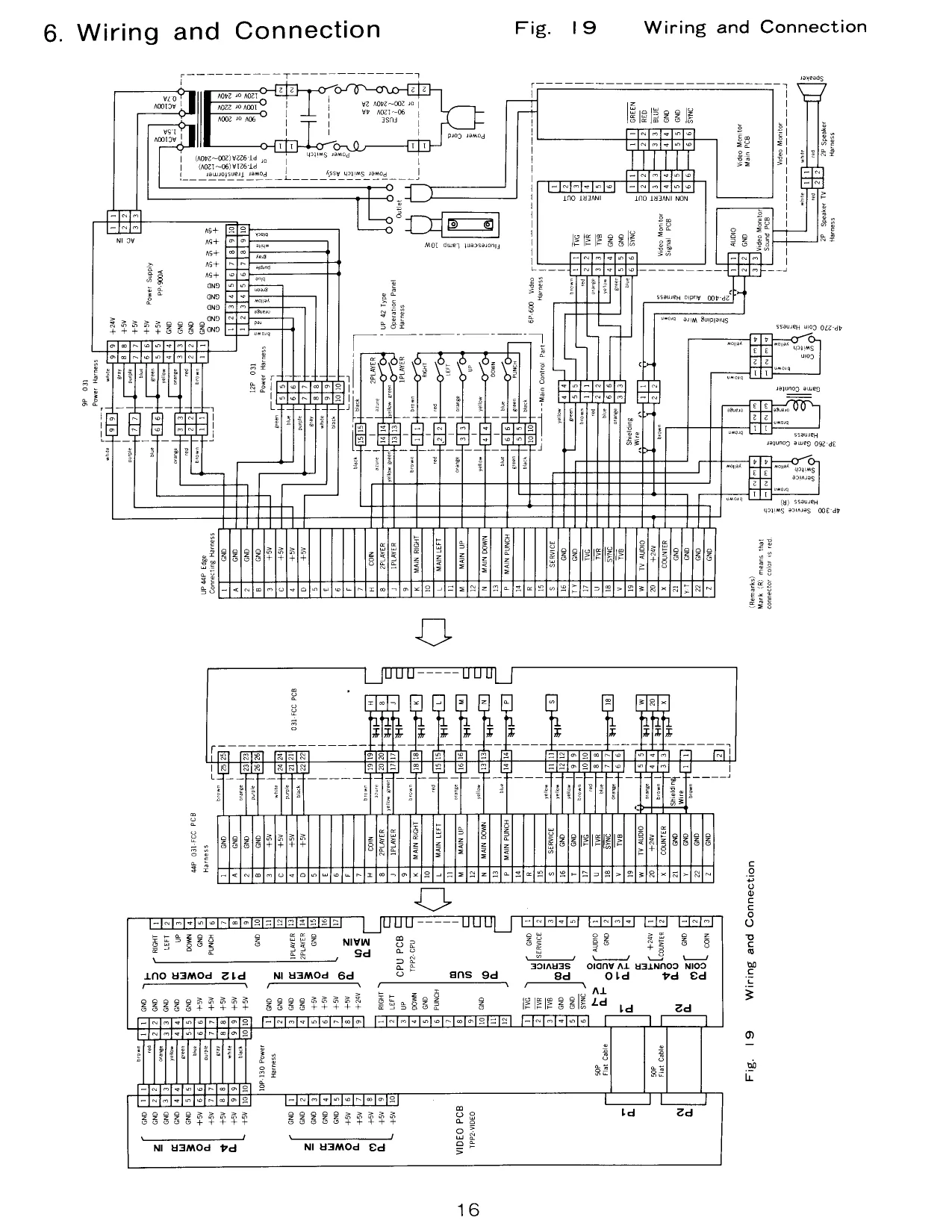
This page is a drawing, shown as the original scan.
- Name of each part and Parts List
Fig. 20 Front View of Game Cabinet
PARTS LIST: TPP2-UP Game Cabinet Assembly Continued
ITEM PART No. DESCRIPTION
| 1 | TPPU-01-01-01 | Body (Wooden Game Cabinet) |
| 2 | TPPU-01-24 | POPEYE Display Panel |
| 3 | TKGU-01-29 | Fluorescent Lamp Ass’y |
| 4 | TPPU- 01-23 | POPEYE Front Screen |
| 5 | TKGU-01-53 | Front Screen Frame (Lower Retainer) |
| 6 | TPPU-01-22 | Plastic POPEYE Operation Panel |
| 7 | TKGU-01-31 | Operation Panel Clamp A (2 Required) |
| 8 | TKGU-01-01-03 | Cash Box |
| 9 | TKGU-01-28 | Coin Door Ass'y |
| 10 | TKGU-01-04 | Coin Door Lock |
| 11 | TPPU-01-02 | Coin Selector: Order By Currency |
TPPU-01-02 Coin Selector 730A (For 25cent)
| 12 | TPPU-01-02-01 | Coin Switch: Order By Coin Selector |
TPPU-01-02-01 Coin Switch D2MC-01F1 (For 730A)
| 13 | TKGU-01-11 | Game Counter |
| 14 | TKGU-01-33 | Service Switch |
| 15 | TKGU-01-64 | Service Switch Bracket |
| 16 | TKGU-01-43 | Speaker |
This page carries no recoverable text. It is a drawing or a photograph. See the original scan.
PARTS LIST: TPP2-UP Game Cabinet Assembly Continued
ITEM PART No. DESCRIPTION
| 1 | TKGU-01-01-05 | Rear Panel |
| 2 | TKGU-01-03 | Rear Panel Lock |
| 3 | TPPU-01-68 | Blind Cardboard (Small) |
| 4 | TPPU-01-67 | Black Cardboard Bezel |
| 5 | TPPU-20-00 | Video Monitor [32 Type] 20-EZV (R-C) |
or TKGU-20-00 Video Monitor [31 Type] 20-EZV (R-B)
| 6 | TPP2-06-00 | TPP2-VIDEO Complete PCB Assembly |
| 7 | TPP2-07-00 | TPP2-CPU Complete PCB Assembly |
| 8 | TPP2-01-20 | Dual Locking-head PCB Spacer 10N(8 Req'd) |
| 9 | TPPU-01-01-10 | Shield Cage |
| 10 | TPPU-01-01-11 | Shield Cover |
| 11 | TPPU-01-01-12 | 031-FCC PCB |
| 12 | TKGU-01-65 | Strain Relief Bushing Plate |
| 13 | TKGU-01-10 | Strain Relief Bushing |
| 14 | TKGU-01-08 | Power Cord: Order By Voltage & Plug Type |
| 15 | TPPU-10-00 | Power On/Off Switch Ass'y (For 90~120V) |
| 15 | TPPU-11-00 | Power On/Off Switch Ass’y (For 200~240V) |
| 16 | TPP-08-00 | PP-900A Complete Power Supply Assembly |
| 17 | TPPU-09-01-01 | PT-921A Power Transformer (For 90~120V) |
| 17 | TPPU-19-01-01 | PT-922A Power Transformer (For 200~240V) |
| 18 | TKGU-01-01-02 | Transformer Base |
| 19 | TKGU-09-01-03 | Terminal Block 6-Position Type |
| 19 | TKGU-19-01-03 | Terminal Block 4-Position Type |
| 20 | TKGU-09-01-02 | Outlet Through Isolation Transformer |
| 21 | TKGU-01-30 | Caster (2 Required) |
Fig. 22 Operation Panel Assembly
PARTS LIST: TPP2-UP Operation Panel Assembly
ITEM PART No. DESCRIPTION
| 1 | TKGU-23-50 | Complete 4 way Controller Ass’y | |
| 2 | TKGU-23-21 | Switch Collar | |
| 3 | TKGU-23-51 | 4 way Guide Plate | |
| 4 | TKGU-23-17 | Switch Spacer (4 Required) | |
| 5 | TKGU-23-16 | Bearing Bracket | |
| 6 | TKGU-23-19 | Shaft | |
| 7 | TKGU-23-20 | Spring Stopper | |
| 8 | TKGU-23-22 | Lever Spring | |
| 9 | TKGU-23-23 | E Ring 4 | |
| 10 | TKGU-23-13 | Control Switch (4 Required) | |
| 1 | TKGU-01-01-04 | Wooden Operation Base | |
| 12 | TKGU-01-55 | Operation Panel Clamp B | |
| 13 | TPPU-01-22 | Plastic POPEYE Operation Panel | |
| 14 | TKGU-23-14 | Blind Plate | |
| 15 | TKGU-01-39 | Controller Ass’y Mounting Plate | |
| 16 | TKGU-01-70 | Controller Knob Plate | |
| 17 | TKGU-23-29 | Controller Knob Collar | |
| 18 | TKGU-01-41 | Controller Knob | |
| 19 | TKGU-23-12 | Switch Button Bracket (3 Required) | |
| 20 | TKGU-23-10 | Button Micro-switch VL105L2 (3 Required) | |
| 21 | TKGU-23-26 | Nut Plate (3 Required) | |
| 22 | TKGU-23-34 | Pal Nut (3 Required) | |
| 23 | TKGU-23-31 | Blue Button Ass’y | (For 1P, 2P) |
| 24 | TKGU-23-32 | Orange Button Ass’y (For Punch) |
PARTS LIST: TPP2-UP Wiring Harness
PART No. DESCRIPTION See Fig. 19 TPPU-93-01 UP 44P Edge Connecting Harness TPPU-93-31 44P 031-FCC PCB Harness TPPU-93-02 2P-400 Audio Harness (400mm) TPPU-93-07 6P-600 Video Harness (600mm) TPPU-93-03 3P-260 Game Counter Harness (260mm) TPPU-93-04 4P-300 Service Switch Harness (300mm) TPPU-93-05 4P-270 Coin Harness (270mm) TPPU-93-06 4P-270 Double Coin Harness (270mm) TKGU-13-06 2P Speaker TV Harness [2P-370] (370mm) TKGU-13-17 2P Speaker Harness [2P-860] (860mm) TPPU-93-08 9P 031 Power Harness (9P-9P Connector) TPPU-93-09 12P 031 Power Harness (10P-12P Connector) TPPU-93-10 UP 42 Type Operation Panel Harness DJRU-13-12 50P Flat Cable [50P-40] (2 Required) TPPU-93-11 10P-130 Power Harness (130mm) or DJR-89-11 10P Power Harness [10P-180] (180mm)
PARTS LIST: TPP2-CPU PCB Assembly Continued
No. DESCRIPTION (Reference Designations and Locations) TPP2-07-00 TPP2-CPU Complete PCB Assembly
| TPP2-07-01 | Z80A Microprocessor | (5J) | |
| TPP2-07-02 | AY-3-8910 Audio I/O MOS LSI with Heat Sink | (7L) | |
| TPP2-07-03 | 2764 8K byte EPROM 300 nsec. : TPP2-C-7Ab_ | (7A) | |
| TPP2-07-04 | 2764 8K byte EPROM 300 nsec. : TPP2-C-7Bb | (7B) | |
| TPP2-07-05 | 2764 8K byte EPROM 300 nsec. : TPP2-C-7Cb | (7C) | |
| TPP2-07-06 | 2764 8K byte EPROM 300 nsec. : TPP2-C-7Eb | (7E) | |
| TPP2-07-07 | MB7051 32x 8bit Bipolar ROM: TPP2-C-3A | (3A) | |
| TPP2-07-08 | MB7051 32x 8bit Bipolar ROM : TPP2-C-4A | (4A) | |
| TPP2-07-09 | MB7052 2564 bit Bipolar ROM : TPP2-C-5A | (5A) | |
| TPP2-07-10 | MB7052 2564 bit Bipolar ROM : TPP2-C-5B | (5B) | |
| TPP2-07-11 | Selected Decoder | : TPP2-C-7J | (7d) |
| TPP2-07-12 | PLA | : TPP2-C-3E | (3E) |
| TPP2-07-13 | PLA | : TPP2-C-4E | (4E) |
| TPP2-07-14 | PLA | : TPP2-C-6E | (6E) |
| TPP2-07-15 | PLA | : TPP2-C-6F | (6F) |
| TPP2-07-16 | PLA | : TPP2-C-6H | (6H) |
| TPP2-07-17 | TMM2016 2K byte RAM 200 nsec. | (7H) | |
| TPP2-07-18 | 28 Pin ALU Custom Chip | (7K) | |
| TPP2-07-19 | 75471 Dual 2-input NAND Driver | (1P) | |
| TPP2-07-20 | 7437 Quad 2-input NAND Buffer | (5H) | |
| TPP2-07-21 | 74123 Dual Retriggerable Monostable | (3M) | |
| TPP2-67-01 | 74LSO0 Quad 2-input NAND | (1B, 1D, 4L, 8D) | |
| TPP2-07-22 | 74LS02 Quad 2-input NOR | (2K, 3L, 5E, 6C, 8E) | |
| TPP2-67-02 | 74LS04_ Hex Inverter | (1A, 4H, 4K) | |
| TPP2-67-03 | 74LSO8 Quad 2-input AND | (3d) | |
| TPP2-07-23 | 74LS14 Hex Schmitt-Trigger Inverter | (3N) | |
| TPP2-67-04 | 74LS20 Dual 4-input NAND | (5D) | |
| TPP2-67-05 | 74LS74 Dual D Type Flip-Flop | (1C, 1L, 2D, 3K, 6D) | |
| TPP2-07-24 | 74LS109 Dual J-K Flip-Flop | (5F) | |
| TPP2-07-25 | 74LS138 Single 3 to 8 Line Decoder | (1E) | |
| TPP2-67-06 | 74LS139 Dual 2 to 4 Line Decoder | (8C, 8F) | |
| TPP2-07-26 | 74LS151 8 to 1 Line Data Selector | (5N) | |
| TPP2-67-07 | 74LS161 Synchronous 4 bit Counter | (1F, 2F, 2E, 2L) | |
| TPP2-07-27 | 74LS240 Octal Inverted Buffer | (2P, 3P, 4M) | |
| TPP2-07-28 | 74LS245 Octal Bus Transceiver | (6N) | |
| TPP2-67-08 | 74LS367 Hex Bus Driver | (2H, 3H) | |
| TPP2-07-29 | 2SC1815 Silicon NPN Transistor | (Q1, 2, 4, 6, 8) | |
| TPP2-07-30 | 2SA1015 Silicon PNP Transistor | ( | 7,9) |
| TPP2-67-09 | 181595 Diode | (D1, 2, 6) | |
| TPP2-07-31 | 1S2076 Diode | (D3, 4, 5, 13) | |
| TPP2-07-32 | 1S85277B Diode | (D7) |
TPP2-07-33 DAN401 Quad Cathode-common Diode Array (DA1~6)
No. DESCRIPTION (Reference Designations and Locations) TPP2-67-10 330pf 50V Ceramic-Disc Capacitor (C5, 6) TPP2-07-34 680pf 50V Ceramic-Disc Cap. (C40)
| TPP2-67-11 | 1000 pf 50V Ceramic-Disc Cap. | (C1) |
TPP2-07-35 .01uf 50V Ceramic-Disc Cap. (C14, 19) TPP2-67-12 .01uf 50V Ceramic-Disc Cap. (C50 ~ 113) TPP2-07-36 .047uf 25V +20% Ceramic-Disc Cap. (C4) TPP2-07-37 .068uf 25V Ceramic-Disc Cap. (C17, 20,21) TPP2-07-38 3.3uf 16V Al Electrolytic Radial Cap. (C7, 18)
| TPP2-07-39 33uf | 16V Al Electrolytic Axial Cap. | (C3, 15) |
| TPP2-07-40 47uf | 16V Al Electrolytic Axial Cap. | (C13) |
TPP2-67-13 220uf 16V Al Electrolytic Axial Cap. (C12)
| TPP2-07-41 | 10 uf | 10V Tantalum Radial Cap. | (C16) |
TPP2-07-42 0 Ohm Shunt Lead (R84, 85)
All discrete R are Carbon Resistors TPP2-07-43 51 Ohm 1/4W +5% Resistor (R35, 39,43, 47, 67) TPP2-07-44 1000Ohm 1/4W +5% Resistor (R36, 40, 44, 51, 63) TPP2-07-45 1100Ohm 1/4W +5% Resistor (R3) TPP2-07-46 220Ohm 1/4W +5% Resistor (R18, 21, 23, 26, 29,31) TPP2-67-14 330O0hm 1/4W +5% Resistor (R34, 38, 42, 46, 66, 82) TPP2-07-47 360Ohm 1/4W +5% Resistor (R37, 41, 45) TPP2-07-48 4700hm 1/4W +5% Resistor (R10, 13, 15, 17, 20, 22, 25, 28, 30, 49,50) TPP2-07-49 680 Ohm 1/4W +5% Resistor (R9, 12, 14,48) TPP2-07-50 8200Ohm 1/4W +5% Resistor (R1, 2) TPP2-67-15 1K Ohm 1/4W +5% Resistor (R16, 19, 24, 27,73, 74, R9O~98)
| TPP2-07-51 | 1.2K Ohm 1/4W +5% Resistor | (R8, 11) |
TPP2-07-52 2K Ohm 1/4W +5% Resistor (R32,52,53,55,56,58,59) TPP2-07-53 3.3K Ohm 1/4W +5% Resistor (R81) TPP2-07-54 5.1K Ohm 1/4W +5% Resistor (R4, 5, 6, 7, 65, 75) TPP2-07-55 7.5K Ohm 1/4W +5% Resistor (R33) TPP2-07-56 10K Ohm 1/4W +5% Resistor (R80) TPP2-07-57 20K Ohm 1/4W +5% Resistor (R54) TPP2-07-58 30K Ohm 1/4W +5% Resistor (R57, 60) TPP2-07-59 33K Ohm 1/4W +5% Resistor (R71,72) TPP2-07-60 120K Ohm 1/4W +5% Resistor (R61)
| TPP2-07-61 | 510KOhm 1/4W +5% Resistor | (R62, 64) |
TPP2-07-62 Hex 5.1K Ohm Series Resistor Array (RM11) TPP2-07-63 Octal 1K Ohm Series Resistor Array (RM7 ~ 10) TPP2-07-64 Quad 68 Ohm Parallel Resistor Array (RM1 ~6)
TPP2-07-65 8.00 MHz Crystal (X1) TPP2-07-66 4-Station, Single-Throw, DIP Bit Switch (SW1) TPP2-07-67 8-Station, Single-Throw, DIP Bit Switch (SW2) TPP2-67-16 16 Pin DIP IC Socket (3A, 4A, 5A, 5B) TPP2-67-17 28 Pin DIP IC Socket (7A, 7B, 7C, 7E) TPP2-07-68 40 Pin DIP IC Socket (5J, 7L)
| TPP2-67-18 | 10 Pin Connector Receptacle | (P12) |
TPP2-67-19 50 Pin Flat Cable Header (P1, 2)
PARTS LIST: TPP2-VIDEO PCB Assembly Continued
No. DESCRIPTION (Reference Designations and Locations) TPP2-06-00 TPP2-VIDEO Complete PCB Assembly
TPP2-06-01 2764 8K byte EPROM 450 nsec. : TPP2-V-1Eb (1E) TPP2-06-02 2764 8K byte EPROM 450 nsec. : TPP2-V-1Fb (1F) TPP2-06-03 2764 8K byte EPROM 450 nsec. : TPP2-V-1Jb (1J) TPP2-06-04 2764 8K byte EPROM 450 nsec. : TPP2-V-1Kb (1K) TPP2-06-05 2716 2K byte EPROM 450 nsec. or TPP2-06-06 2732 4K byte EPROM 450 nsec. : TPP2-V-5Nb (5N) TPP2-06-07 MB7052 2564 bit Bipolar ROM : TPP2-V-7J (7d) TPP2-06-08 PLA : TPP2-V-5U(5U) TPP2-06-09 PLA : TPP2-V-7H (7H) TPP2-06-10 TMM2016 2K byte RAM 120 nsec. (8P, 8S) TPP2-06-11 2114 1KX4 bit RAM 300 nsec. (5P, 5R, 5S) TPP2-06-12 Special Ordered 2564 bit RAM 300 nsec. : (1S, 2S, 1T, 2T, 2U) TPP2-06-13 Selected 5501 2564 bit CMOS RAM 350 nsec. (1R,2R,1U) TPP2-06-14 MB7063 649 bit Bipolar RAM (1M, 3M, 1P, 3P)
TPP2-06-15 TC40HO04 CMOS Hex Inverter (8L) TPP2-06-16 74S04 Schottky Hex Inverter (7D)
TPP2-67-01 74LSO00 Quad 2-input NAND (3A, 4D, 4S, 5B, 6L, 7L) (5A, 5L, 6A, 6T) TPP2-67-02 74LS04 _ Hex Inverter TPP2-67-03 74LSO8 Quad 2-input AND (2C, 2D) TPP2-06-17 74LS10 Triple 3-input NAND (3D) TPP2-06-18 74LS11_ Triple 3-input AND (4A, 7C) TPP2-67-04 74LS20 Dual 4-input NAND (7B) TPP2-06-19 74LS32 Quad 2-input OR (1D) TPP2-67-05 74LS74 Dual D Type Flip-Flop (4B,5C,6B,8B,8E,8M) TPP2-06-20 74LS86 Quad 2-input EXOR (2A,5D,6F,6H,6J,7K,8C) TPP2-67-06 74LS139 Dual 2 to 4 Line Decoder TPP2-06-21 74LS157 Quad 2 to 1 Line Data Selector (4M,4N, 4P, 5d, 6K, 6P, 6R, 6S, 6U, 7P, 7R, 7S, 8T) TPP2-67-07 74LS161 Synchronous 4 bit Counter (4R)
(5E, 6E, 7E, 7F,8F,8H, 7M, 7N) TPP2-06-22 74LS174 Hex D Type Flip-Flop — (1L,2L,3C,3L,5T,8U) (3U,4C) TPP2-06-23 74LS175 Quad D Type Flip-Flop TPP2-06-24 74LS194 4 bit Shift Register (4E, 4F, 4H, 4J, 4K, 4L, 5F,5K,6M,6N) TPP2-06-25 74LS257 Quad Data Selector (7T, 7U) TPP2-06-26 74LS273 Octal D Type Flip-Flop (8N) TPP2-06-27 74LS283 4 bit Full Adder (3R, 3S, 3T) TPP2-67-08 74LS367 Hex Bus Driver (4T, 4U, 6D) TPP2-06-28 74LS368 Hex Bus Driver (6C) TPP2-06-29 74LS377 Octal D Type Flip-Flop (3E, 3F, 3J, 3K)
(D1) TPP2-67-09 181595 Diode
No. DESCRIPTION (Reference Designations and Locations) TPP2-06-30 33 pf 50V Ceramic-Disc Capacitor (C8)
| TPP2-06-31 | 180 pf SOV Ceramic-Disc Cap. | (C1) |
TPP2-67-10 330 pf SOV Ceramic-Disc Cap. (C2, C3, C4, C6, C7, C10)
| TPP2-67-11 | 1000 pf 50V Ceramic-Disc Cap. | (C5) |
TPP2-67-12 .01 uf 50V Ceramic-Disc Cap. (C50~139) TPP2-67-13 220 uf 16V Al Electrolytic Axial Cap. (CQ)
All discrete R are Carbon Resistors TPP2-67-14 330 Ohm 1/4W +5% Resistor (R1, 2) TPP2-67-15 1K Ohm 1/4W +5% Resistor (R90 ~101) TPP2-06-32 1K Ohm X 9 Parallel Resistor Array (RM1, 2)
TPP2-06-33 20.160 MHz Crystal (X1) TPP2-67-16 16 Pin DIP IC Socket (7J) TPP2-06-34 24 Pin DIP IC Socket (5N) TPP2-06-35 22 Pin DIP IC Socket (AR, 2R, 1U) TPP2-67-17 28 Pin DIP IC Socket (1E, 1F, 1d, 1K, 1M, 1P, 3M, 3P) TPP2-67-18 10 Pin Connector Receptacle (P4) TPP2-67-19 50 Pin Flat Cable Header (P1, 2)
PARTS LIST: PP-900A Power Supply Assembly Continued
No. DESCRIPTION (Reference Designations) TPP-08-00 PP-9800A Complete Power Supply Assembly TPP-08-01 3D-0086 Complete Power Supply PCB Assembly
| TPP-08-02 | 3D-1001 Custom Hybrid IC | (IC1) |
| TPP-08-03 | 2SA817 Silicon PNP Switching Transistor | (TR2) |
| TPP-08-04 | 2SA1015 Silicon PNP Transistor | (TR3) |
| TPP-08-05 | 2SC2535 Silicon NPN Transistor | (TR1) |
| TPP-08-06 | SFOR1B41 or 03PO05M SCR | (SCR1) |
| TPP-08-07 | S4VB40 or 4G4B41 Diode Bridge | (BR1) |
| TPP-08-08 | 1B4B41 Diode Bridge | (BR2) |
| TPP-08-09 | CTB-33S or S10 Schottky Barrier Diode | (D6) |
| TPP-08-10 | 1S1835 Fast-Recovery Diode | (D1, 2, 3, 4) |
| TPP-08-11 | 1S$953 or 181588 Diode | (D5, 8) |
| TPP-08-12 | 18954 Diode | (D7) |
| TPP-08-13 | 05Z 5.6V Zener Diode | (ZD2) |
| TPP-08-14 | 470 pf 2KV Ceramic-Disc Capacitor | (C1, 2,17) |
| TPP-08-15 | 10 uf 16V Al Electrolytic Radial Cap. | (C6, 9, 12) |
| TPP-08-16 | 100 uf 35V Al Electrolytic Radial Cap. | (C8) |
| TPP-08-17 | 220 uf 25V Al Electrolytic Radial Cap. | (C16) |
TPP-08-18 330 uf 200V Al Electrolytic Switching Radial Cap. (C4)
| TPP-08-19 | 470 uf 25V Al Electrolytic Radial Cap. | (C5) |
| TPP-08-20 | 2200 uf 10V Al Electrolytic Radial Cap. | (C10, 11, 15) |
| TPP-08-21 | 1000 pf 50V Film Cap. | (C7) |
| TPP-08-22 | .047 uf 630V Film Cap. | (C3, 13, 14) |
No. DESCRIPTION (Reference Designations)
| TPP-08-23 | 22 Ohm 1/4W Carbon Resistor | (R2) | |
| TPP-08-24 | 51 | Ohm 1/4W Carbon Resistor | (R4, 10, 12) |
| TPP-08-25 | 470 Ohm 1/4W Carbon Resistor | (R5) | |
| TPP-08-26 | 1K Ohm 1/4W Carbon Resistor | (R14, 15) | |
| TPP-08-27 | 20K Ohm 1/4W Carbon Resistor | (R13) | |
| TPP-08-28 | 12 Ohm 1/2W Carbon Resistor | (R3, 9) | |
| TPP-08-29 | 100 Ohm 1/2W Carbon Resistor | (R16) | |
| TPP-08-30 | 1K Ohm 1/2W Carbon Resistor | (R6) | |
| TPP-08-31 | 2 | Ohm 5W Cement Resistor | (R1) |
| TPP-08-32 | 20 Ohm 5W Cement Resistor | (R11) | |
| TPP-08-33 | 1 | Ohm 1W +5% Metal Oxide Film Resistor | (R7) |
| TPP-08-34 | 1K Ohm 3W +5% Metal Oxide Film Resistor | (R8) | |
| TPP-08-35 | .01. Ohm Shunt Resistor | (SH1) | |
| TPP-08-36 | 2K Ohm 1/4W Vertical Cermet Trimpot | (VR1) | |
| TPP-08-37 | 50K Ohm 1/4W Vertical Cermet Trimpot | (VR2) | |
| TPP-08-38 | El-30 Type SD-0086T Switching Transformer | (11) | |
| TPP-08-39 | 28 Type | 3D-1000 Transformer | (T2) |
| TPP-08-40 | EE-16 Type 3D-1000 Oscillator Transformer | (T3) | |
| TPP-08-41 | $C02-100 | SC Coil | (L1) |
| TPP-08-42 | EI-30 Type SD-O086L 25 mH 0.5A Choke Coil | (L2) | |
| TPP-08-43 | SFT12-50 100 uH 5A SF Coil | (L3) | |
| TPP-08-44 | 9 Pin DC Output Connector Receptacle | (QP) | |
| TPP-08-45 | 10 Pin DC Output Connector Receptacle | (10P) |
TPP-08-46 3A SB FGMB NR Type Fuse TPP-08-47 F-6 Fuse Holder TPP-08-48 3D-0086 Type Heat Sink TPP-08-49 Heat Sink Clip (2 per assembly) TPP-08-50 Thermally Conductive Rubber (2 per assembly) TPP-08-51 Nylon PCB Retainer (2 per assembly)
TPP-08-52 3D-0086 Type Metal Frame TPP-08-53 3D-0086 Type Metal Cover : TPP-08-54 3 Pin AC Input Connector Receptacle on Metal Frame
©1982 Nintendo of America Inc. PRINTED IN JAPAN
AX TpP2-cPu ASSEMBLY
©1982 Nintendo of America Inc. u a a v sai ao oN, w 4 iy nog 3 ¢ 2 q M az sanisi io 0019, 62 62 62 $62 ved 62, 162 169 062
brea +=, br
4no_wamos cOS7 os or
eld bet Tr)
i} oF
qvb-9
OLB -E- AV
aei/our
" Praposag parse yan
aq
four LL -9-Zddb 4 9L-2-2ddl VOL ~eddi V9OLZ oF 03018 fig oF
vi
a or
33 Sid
tt = CI
mr vs = toa
Fy 9. Deda Lan
E E a
VS 2-2ddb
B oat g ou
jo Ss] af on ou atc] ol jo our
ists
ore
ooev min ee at e501 an Of +9
ie
®
°
TAS Wo
' Se 2: SOL 2ddl eu LJ
+8 "
Ndd—10—-edd = &
av-9-2ddi [sol dw q+
og
° BE-D-2ddt
&
=
x
OST
we ae
oD
oo ST os or
DoLOUYy jo Opuaju! ra9 ab % oot pr
2os7
vis
Ore S7
va]
wt, ree ia ELA a cry
L9E $7
80ST
vLST oF
as 030th Bq
vigil $7
Lye ST
IN z861©
" n
pLsS7 § a
ae
az
we
z
we
s+ Ope Sq & Eo
ad
“a3- 219 1e9
fm
WEZIK « a
vii ST
a
=x
:
loKexe)
Ge
LS7 00 $7 vO ST
a m9
a+ z
vu
a
NE u3Mod Ca | €d Sposengrr ng? TPP2-01-VIDEO MADE IN JAPAN | ve vamod ©1982 Nintendo of America Inc. or a _ a a a o n 7 va 7 ® ° 8 G3
ro S. a“ we Ea s w O3 @ 23 [os7 zs7¢ 48 bLSTe oos7§ 6 +2 [bes7e 2 a % . ws th sore Oa tee o 43 [essie (re7e 48 99ESTC bLETS #9 [Siis7 g 0 8 al 29 w 3 ots Pi ; . o 43 als FOr “ies T9ES7¢ 9ST 3 9
- as oe. as
ae a * ts nw y a cy e < i) a F Say Tu rey L-A-ddb Wists7g a8 [WIST¢ 2g «(erste 43 he ' a at a
no s8[vigis7¢ visi s7¢ +9 [9357 48
HL-A-Zddb ie « x 4g (ylor es? Wie ¢ a 48 x “ me "9 us Thfeedd 8 3 nr) "et, zo 48 [beste us [asisie PeISTe 48 ne c
x 4g 8" as Tsrsve +2 [oers7e 2 [deste 33 Zies7¢
Oos7e 2 (eos7@ [poste +2 [bers7e 38 [(burstt. =[RUTER (PUSR us 2 uu 1 = w 7 w i. [Sens By te Lys vist si¢ +g[veisi¢ 38 zsIS7¢ ga (esse ~ ne ~ 3} s90Law dq # S90LaU we ve ANS-A-2dd t ZeLz49 91L2 We ° ze €L2 $7 a8 VISTSTe a8[beisne #8 48 WEITERE Fe 7 ee ne me “eo “ “
2esuoor = £90L au UH 3858021 Estste Tsisve 8 [Tee e9oLan 48 | 290 9102 “ . _ 2 d co Led pesoce ES 4 055 mtg Lstsi¢ 48 vile ¢ ber ST ¢ [682572 parsatag JL +] | parzeies 4 432 we us » we g A = az mt ¢ 2g ot ° Wve ° nw ws? LSI ST * Cite? [oosa¢ [EBZS7 2 28 [pesapso persis} $8 [pasepuo yiads 28H s° se ” so. sz 3
ao g Wve ° Wve ° 448 3 LI STC LEST CBEST #8 |pasapig sods 48 para hy Bronds4 ag
vo NS-A-@ddl oc 4 +3 (ks@s7¢ ig [Ls 80 wad ¢ ISEST< 42 BC me me bah cs wo nw id s + , 2,9 cS 3 . 80,3
B tpp2-viDEO ASSEMBLY ©1982 Nintendo of America Inc.
This page reads as a drawing: its text was drawn rather than typeset, and comes out in fragments. See the original scan.
This page reads as a drawing: its text was drawn rather than typeset, and comes out in fragments. See the original scan.
This page reads as a drawing: its text was drawn rather than typeset, and comes out in fragments. See the original scan.
This page reads as a drawing: its text was drawn rather than typeset, and comes out in fragments. See the original scan.
This page reads as a drawing: its text was drawn rather than typeset, and comes out in fragments. See the original scan.
This page reads as a drawing: its text was drawn rather than typeset, and comes out in fragments. See the original scan.
{] irri
HEAT
SINK
INPUT
AC O | es BE 02 PP—900A ca
R201 3 less Op2 BRI
FUSE 3A
P100V cs OUTPUT
}00V 50/60 HE cB f2 100 pF 35¥ oa eno t——Wwy-—4 a &[ale[sfo]oJe fo) i] ol-
PP-900A POWER SUPPLY | SCHEMATIC AND ASSEMBLY ©1982 Nintendo of America Inc. BR2 1B4B41 alesse [=[o1=
VR1 2ka Yaw
+5y Voltage Adjust
77] TR3 2saiois
SCRI
SFOR1B41 ‘or 03PO5M, Over ~Voltage Protection RI4 1ka VvR2 5oKn Yaw Current Fold Back Adjust
CONTROL CIRCUIT BOARD U885493 ry - ‘R205 ~ TA207 187078, or ZSC945L (P.O) a3 = rome ven
| 1 | SUFFER | (Gaammey(ENTEW | Br] |
Vass vase
| (e} | Book | Shoe | tx |
saoum |e] Seeor fe. mao {|S Focus acorao | 18 voLuMe Ges 8% BRA, TO MAIN CHASSIS CIRCUIT BOARD.
e
wool eK ‘og i eo mint sas
a
| ; | ASE | su301 | (uEzs04t) | ar | |
| : | ‘tk | Eco | Be | ge | are |
rt = LU 7668 KGD Kae prow wan ois CINGUT BOARD At rs oe 1. TRANSISTOR BASE INFORMATION.
¢ © axon
| oo | ae | Ty | Baie |
eee 1 (RATS. cies ne nun
| co | Bods | ‘outage. AEQULATOR | a, |
| arg | a | res | |
| i | ¢ | at |
=
co =a
| - | ||| | Bae. | fee | zm |
ms S| || aaa sce 40K WIZ Acioor se
- RESISTOR, CAPACITOR: INFORMA © RESISTOR — INFORMATION. OM
| VTL | ase | rece |
AESISTOR VALUE IN. See AS. TO 1/4 PTVPE RESISTORS, eT vPe AraStons,nesist. ced les Keone ARES AE CAPACITOR — INFORMATION EXPRESSED IN P WHEN THE UNIT ISPE- OTHERWISE OMITTED. RATING VOLTAGE (THE UNIT AS 70 “soy, CTYPE" CAPACITORS VALU Sony ewen, ual
- THIS BEING A FUNDAMENTAL SCHEMATIC THERE WILL BE SOME CASES THAT THE REAL CIRCUIT DOES NGT COINCIDE WITH THIS, RESISTOR TP! F: INSULATED FIXED CARBON FILM RESISTON f
- NN: INSULATED METAL FILM FIXED RESISTOR. R; INSULATED FIXED METAL OXIDE FILM RESISTOR. INSULATED WIRE WOUND FIXED RESISTOR. €; FIXED CARBON COMPOSITION RESISTOR. RMLE or s180-02 wise swan Raat tox Yoox. . ir Rat J 9307
Wear LAtaee be
CAPACITOR TYPE
FIXED CERAMIC CAPACITOR,
RADIAL TRE ALUMINUM & F ; POLYESTER rit capaciTOR, = BE Sresbaai R! POLYPROPYCENE Fits CAPACITOR, (Pi: NON POLAR atusinu =
| MAIN CHASSIS CIRCUIT BOARD | _U 885486 | _ | A | EEN 88 | _ | =~ | ELECTROLYTIC CAPACITOR. |
rast ‘to Bez. Fsbae9, 2s0es8A.0s Mon, DRIVE mon. oureUT
20-EZV(R-C) SCHEMATIC J Sheet 1 of 2
©1982 Nintendo of America Inc.
FROM pat MAIN CIRCUIT BOARD AB AM, 4 oO > AS
| Ri0z | Rios rT” Orel | coq | C105 | D10F | ||
| ask | vk, | EGAC-06 «= G- BUFFER | e01 ere |e | E@aol-12 | 4 |
; Los
| A | G-GAIN | «re | 102 |
aint 536(R.&)
| + GREEN | rio | reese | asc | ac | |||
| ? pep RIO} | Sco | (yY | i wut | i | ||
| reo yay | €) | {K) ie | INVERT OUT | |||
| [ _|axouxo | 26 put | 104 | a | |||
| i | ne | ees | SK Mo | ap | Pak | tue |
cuz Rae Rat 227 2K Lk FROM Rie MAIN CIRCUIT BOARD
BAZ
NON INVERT OUT
SIGNAL CIRCUIT BOARD uyRo0z4
> WARNINGS ~~ | 1. Service work should only be performed by a qualified i} service technician. | 2. An isolation transformer must be used between the Ac | supply and the AC plug of the monitor before servicing | or testing is performed since the chassis and the heati} sink are directly connected to one side of the AC line i} which could present a shock hazard. i} Supply voltage of the video monitor : Ac 90Y - 1104 i] 50/60 Hz { 3. X-RAY RADIATION WARNING AND PRODUCT SAFETY NOTICE ! | This video monitor contains circuits and components | included specifically for safety purpose { For continued protection, no changes should be made to i} original design, and components identified by shading i] and by ¢ A > on schematic diagram should be replaced 1 with exact factory replacement parts. i] DO NOT degrade the safty of the set through improper | servicing. 20-EZV(R-C) SCHEMATIC K Sheet 2 of 2 ©1982 Nintendo of America Inc.