Crystal Castles SP-241 1st Printing
Crystal Castles (version 4) (Atari, 1983) · Schematic Package · 21 pages · 60 sections · original scan
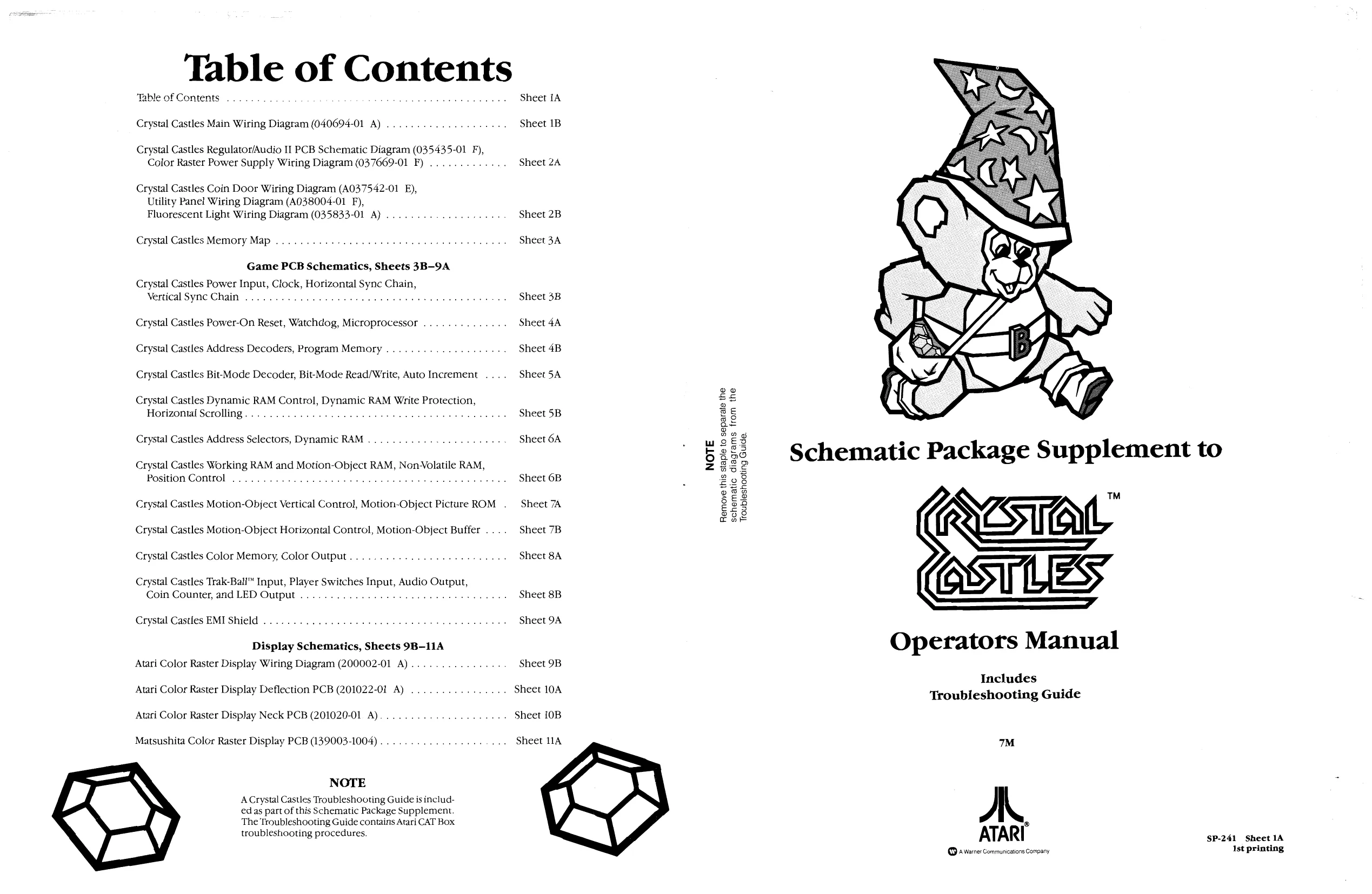
Table of Contents
Table of Contents
Crystal Castles Main Wiring Diagram (040694-01 A) .
Crystal Castles Regulator/Audio II PCB Schematic Diagram (035435-01 F), Color Raster Power Supply Wiring Diagram (037669-01 F) ..........0.
Crystal Castles Coin Door Wiring Diagram (A037542-01 E), Utility Panel Wiring Diagram (A038004-01 F), Fluorescent Light Wiring Diagram (035833-01 A) ........-...5-
Crystal Castles Memory Map
Game PCB Schematics, Sheets 3B-9A Crystal Castles Power Input, Clock, Horizontal Sync Chain, Vertical Sync Chain . .
Crystal Castles Power-On Reset, Watchdog, Microprocessor ........
Crystal Castles Address Decoders, Program Memory ....... « bans oeeeem &
Crystal Castles Bit-Mode Decoder, Bit-Mode Read/Write, Auto Increment ... .
Crystal Castles Dynamic RAM Control, Dynamic RAM Write Protection, Horizontal Scrolling..................
Crystal Castles Address Selectors, Dynamic RAM ........... +
Crystal Castles Working RAM and Motion-Object RAM, Non-Volatile RAM, Position Control . 2.0... 6.06... . eee serene os gee :
Crystal Castles Motion-Object Vertical Control, Motion-Object Picture ROM .
Crystal Castles Motion-Object Horizontal Control, Motion-Object Buffer .
Crystal Castles Color Memory, Color Output .
Crystal Castles Trak-Bali™ Input, Player Switches Input, Audio Output, Coin Counter, and LED Output ...... 2.00.00 0 202 eee ee eee
Crystal Castles EMI Shield ............. tae rages Gis 2
Display Schematics, Sheets 9B-11A Atari Color Raster Display Wiring Diagram (200002-01 A) .
Atari Color Raster Display Deflection PCB (201022-01 A) ..........-..
Atari Color Raster Display Neck PCB (201020-01 A).....
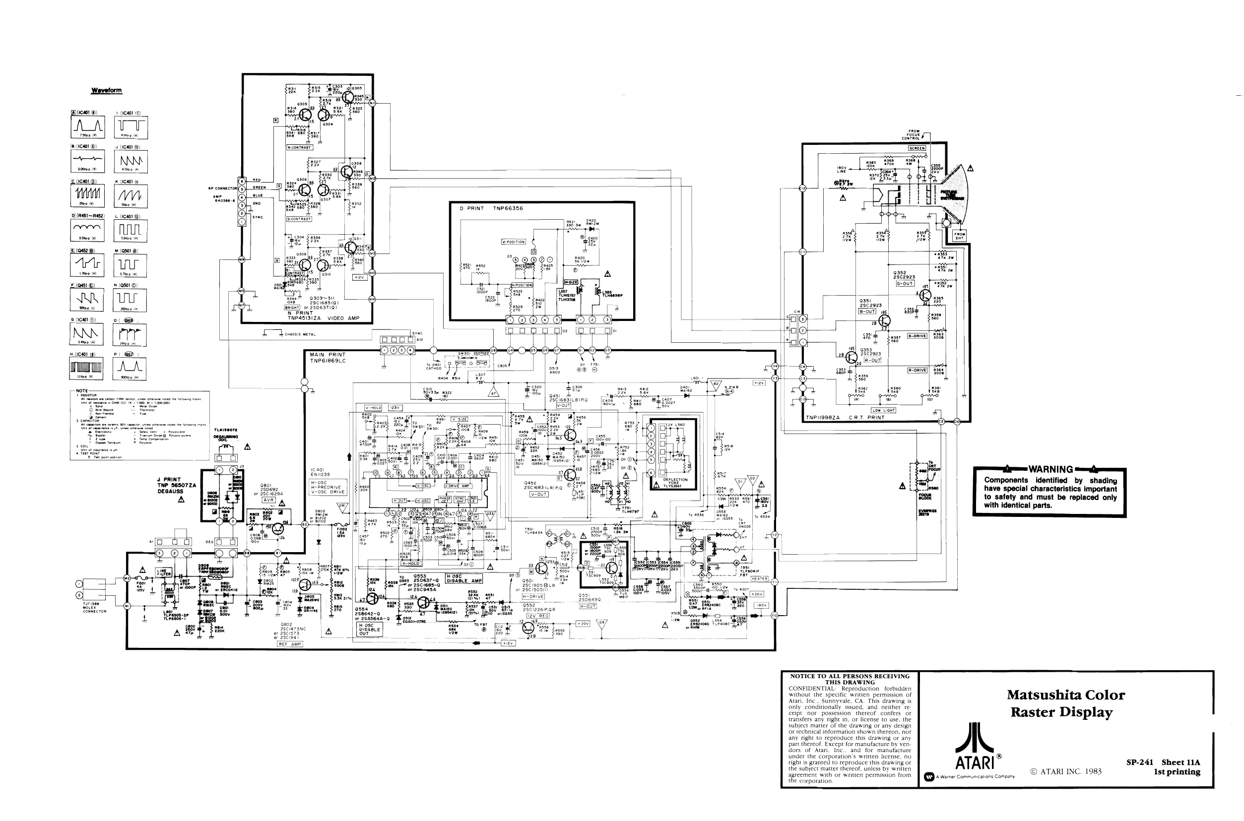
Matsushita Color Raster Display PCB (139003-1004)
Sheet 1B
Sheet 2A
Sheet 2B
Sheet 3A
Sheet 3B
Sheet 4A
Sheet 4B
Sheet 5A
Sheet 5B
Sheet 6A
Sheet 6B
Sheet 7A
Sheet 7B
Sheet 8A
Sheet 8B
Sheet 9A
Sheet 9B
. Sheet 10A
. Sheet 0B
Sheet 11A
™
Operators Manual
Includes Troubleshooting Guide
™
AL ‘2 ATARI SP-241 Sheet 1A © Aarne: Communications Company Ist printing
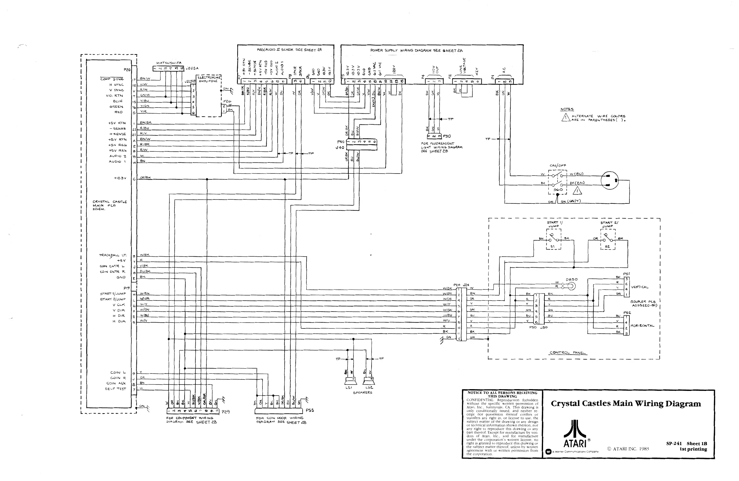
This page is a drawing, shown as the original scan.
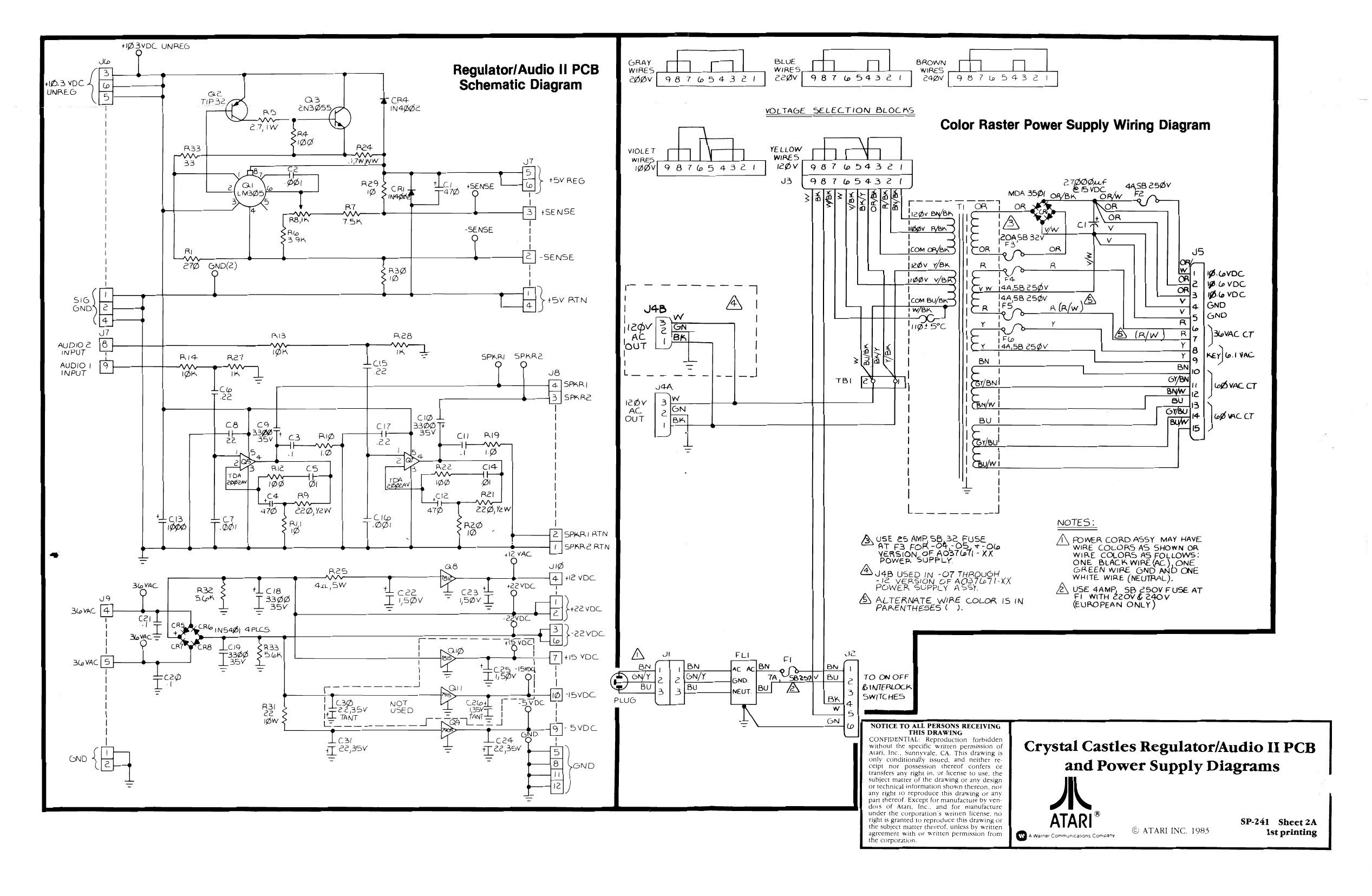
This page is a drawing, shown as the original scan.
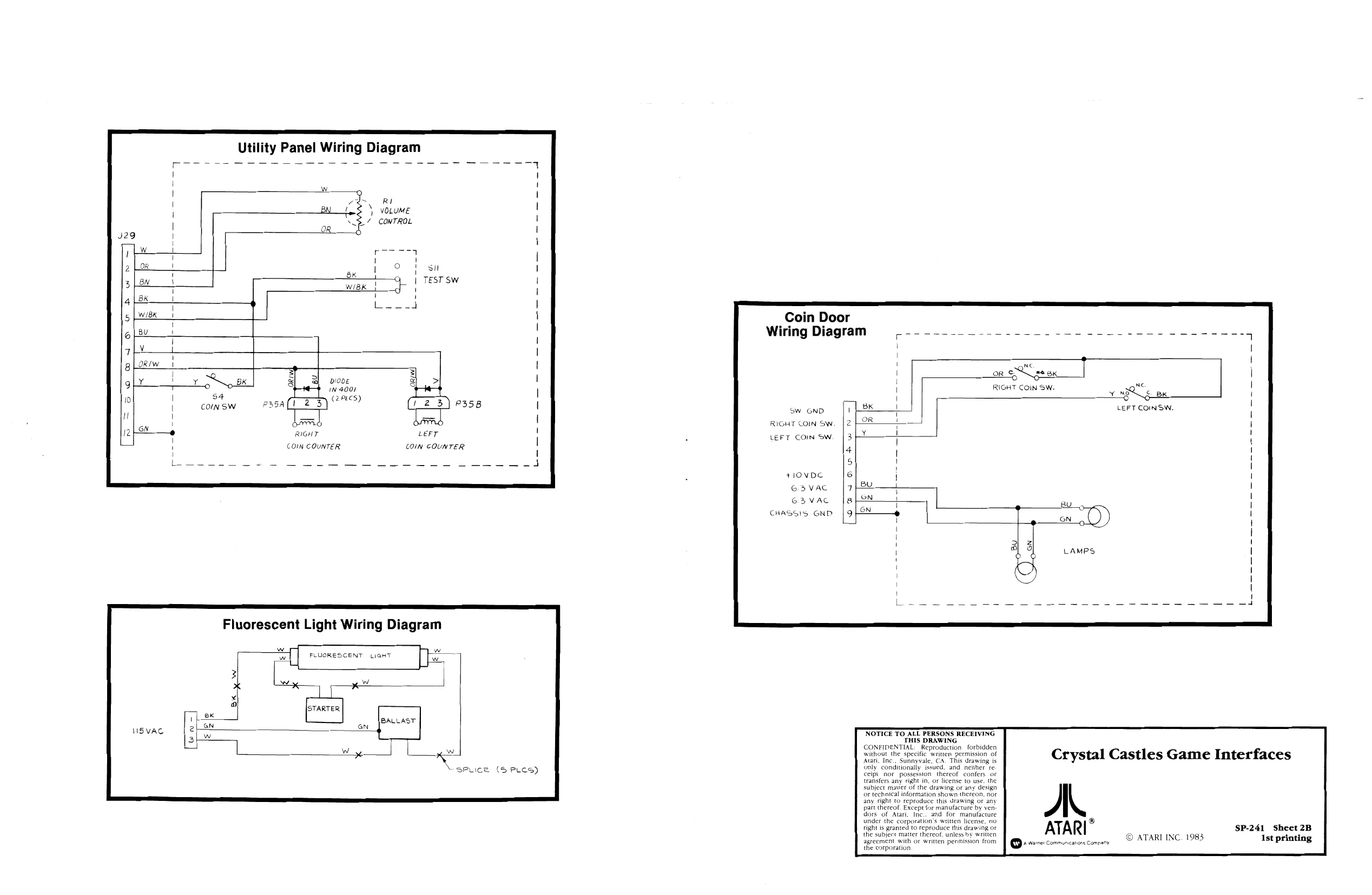
So aIdA GH
Utility Panel Wiring Diagram
y Sy 8K
COIN SW
RIGHT.
COIN COUNTER >|
- °358
LeFr
COIN COUNTER
Fluorescent Light Wiring Diagram
w.
OK FLUORESCENT
x uaHT
eranteR
on
wy — | | a “spiice (5 PLes)
Coin Door
Wiring Diagram
Sw GND.
RIGHT COIN SW
LEFT COIN SW.
+IOVDE
6.3 VAC
63 VAC
CHASSIS GND RIGHT COINSW. wns ox
NOTICE TO ALL PERSONS RECEIVING THIS DRAWING CONFIDENTIAL: Reproduction forbidden without the specific weitten permission of
Atari, Inc., Sunnyvale, CA. This drawing is
only conditionally issued, and nekher te ceipi_nor possession thereof confers or transfers any Fight in, or license to use, the subject mavier of the drawing or any design Or technical information shown thereon, nor any right to repraduce this drawing of any part thereof. Except for manufacture by ven dors of Atari, Inc... and for manufacture Under the corporation's written license, 110 right is granted to reproduce this drawing or
the subject matter thereof, unless by written
agreement with or written permission from the corporation LEFT COINSW.
Crystal Castles Game Interfaces
A ATARI” © ATARI INC. 1983 SP-241 Sheet 2B Ist printing
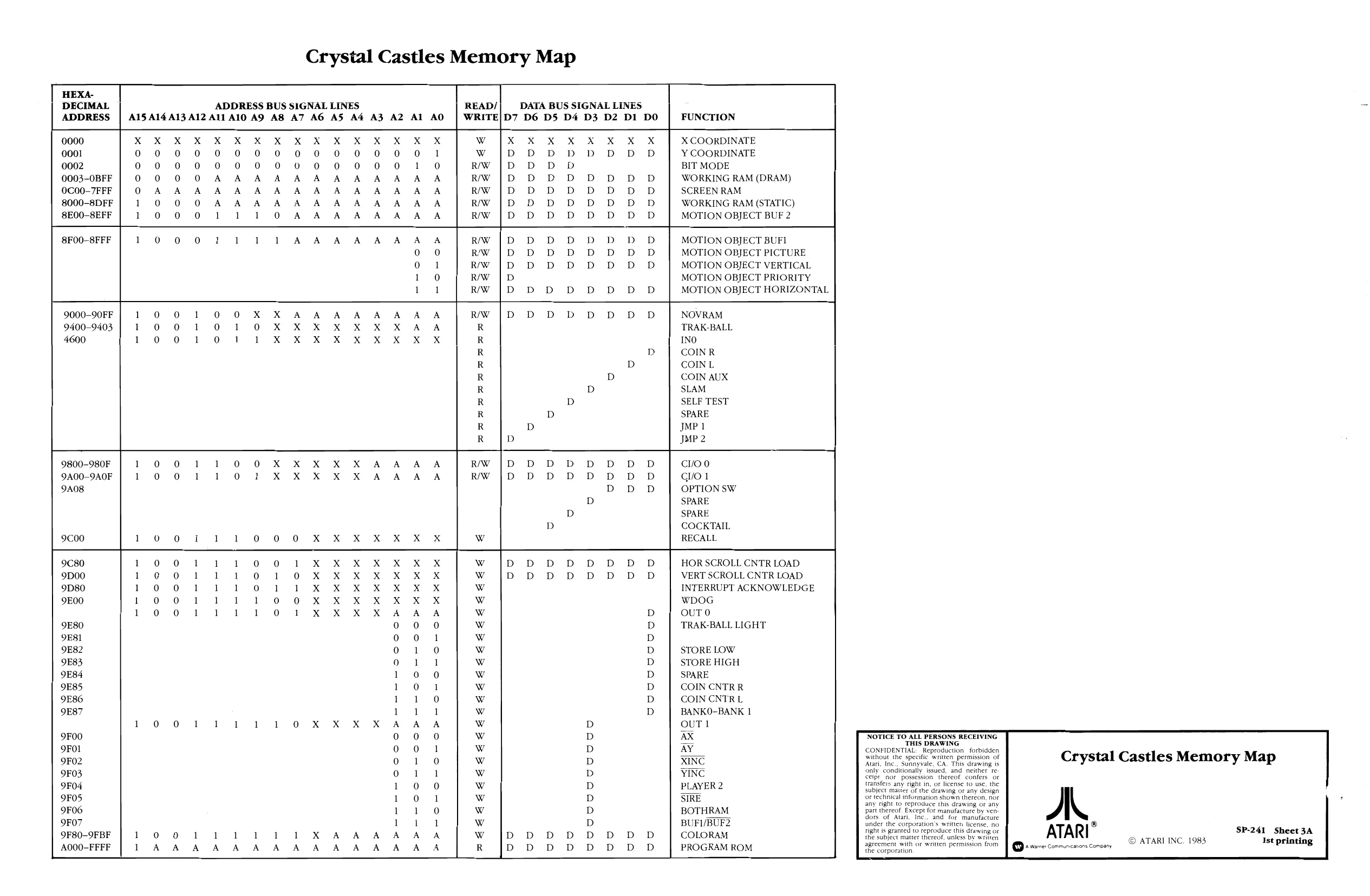
Crystal Castles Memory Map
7. DECIMAL ADDRESS BUS SIGNAL LINES READ/| DATA BUS SIGNAL LINE: ADDRESS A15.A14A13 Al2 All A10 AO A8 A7 AG AS A4 AZ A2 Al AO WRITE|D7 D6 D5 D4 D3 D2 D1 DO FUNCTION
0000 kX KX K KX X X KX X X X X X X X XK X Ww X X X X X X X X X COORDINATE
0001 0 0 0 0 00 00 00 0 0 0 0 0 1 Ww DDDObDD DOD OD Y COORDINATE
| 0002 | 0000 00 00000000 10 RW }]D DD D | BIT MODE |
0003-OBFF 0 0 0 0 A A A A A A A A A A A A RW DDODODODODOD OD WORKING RAM (DRAM) 0C00-7FFF oO A A A A A A A A A A A A A AA RW DDODODODODODOD SCREEN RAM 8000-8DFF 1 0 0 0 A A A A A A A A A A AA RW DDODODODODOD OD WORKING RAM (STATIC) 8E00-8EFF 1 0 0 0 1 1 1 o A A A A A A AA RW DD DOD DOD DOD MOTION OBJECT BUF 2
8FO0-8FFF 1 0 00 1 1 1 1 A A A A A A AA RW DDODODODD YD D MOTION OBJECT BUFI 0 0 RW DDoODoODODODOD D MOTION OBJECT PICTURE 01 Rw 1D D DD D D D D_ | MOTIONOBJECT VERTICAL 1 0 RW D MOTION OBJECT PRIORITY, 1 1 RW DDD DODD ODD MOTION OBJECT HORIZONTAL,
9000-90FF} 1 0 0 100 X X AAAAAAAA Rw }D DD bD DD D D | NovRAM 9400-9403 1 0 0 1 ool oO X X X KX X X X A A R TRAK-BALL
| 4600 | 1 0 0 1 ool 1X X KX X X X XK X X R | INO |
R dD COIN R
| R | D | COIN L |
| R | D | COIN AUX |
| R | D | SLAM |
| R | D | SELF TEST |
| R | D | SPARE |
| R | D | JMP 1 |
R dD JMP 2
9800-980F | 1 0 0 1 10 0X X X X X A AAA RIW D DD | coo 9ao0-9A0F | 1 0 0 1 1 0 1 X X X X X A AAA rw |D DD DD dD dD »D *'| qi 9A08 D D D | OprioNsw SPARE SPARE COCKTAIL
| 9C00 | 1 0 071 1 1 0 0 0 X X X KX KX XK X | RECALL | |
| 980 | 1001 1 100 1X X X X X X X | HOR SCKOLL CNTR LOAD | |
| 9D00 | 1001 1 101 0X X X X X X X | DDDODODOD | VERT SCROLL CNTR LOAD |
| 9D80 | 1001 1 101 1X X X X X xX x | INTERRUPT ACKNOWLEDGE | |
| 9E00 | 1 0 0 1 1 1 1 o o Xx X X X X X X | WDOG |
1 0 0 1 1 1 1 0 1 X X X X A A A D OUT O
| 9E80 | 0 0 0 | D TRAK-BALL LIGHT |
| 9E81 | 0 0 1 | D |
| 9E82 | 0 10 | Db | sTORELOW |
| 9E83, | 0 1 1 | D STORE HIGH |
| 9E84 | 10 0 | D | SPARE |
| 9E85 | 1 01 | D | COINCNTRR |
| E86 | 1 1 0 | D COIN CNTRL |
| 9E87 | 1101 | D_ | BANKO-BANK 1 |
| 100 1 1 1 1 10x X X X AAA | D | OUT 1 |
9FOO 0 0 0 D AX NOTICE TO ALL PERSONS RECEIVING
| 9FO1 | 001 | D | AY | CONFIDENTIAL. Reproduction forbidden | ||
| oFo2 | 0 1.0 | D | witout se spell een mc of | Crystal Castles Memory Map | ||
| 9F03 | o 11 | D | YINC | cant ‘aor pomesion thereor confers. or | ||
| 9F04 | 1 0 0 | D | PLAYER 2 | Subjeet nutter St tne drawing or any design | ||
| 9FO6 | 1 1 0 | D | BOTHRAM | Bin theror ixcepe tor manuactre by ver | ||
| 9FO7 | 1 iol | D | BUFI/BUF2 | ‘der the corporation’: writen eense, no | ® | |
| oF80-O8FBF | 1 0 0 1 1 1 1 1 1 X A AA AAA | DDDDODODD COLORAM | Te ipBer mater thereof unless by won | ATARI | . | cos | SP-241 Sheet 3A |
| A000-FFFF 1 A A A A A A A A A A A A A A A | DDoDODODODOD PROGRAM ROM | agreement with or writen permasion fom J @Yeaarerconmncrionscemoay © ATARI INC. 1983 | Mepentne |
the corporation
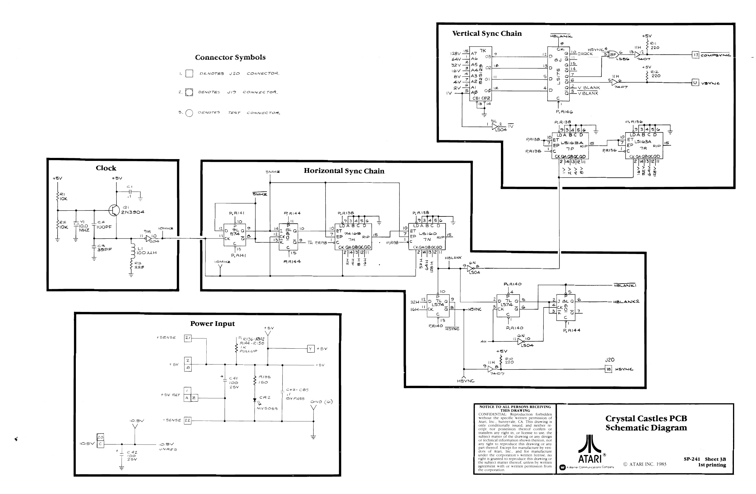
This page is a drawing, shown as the original scan.
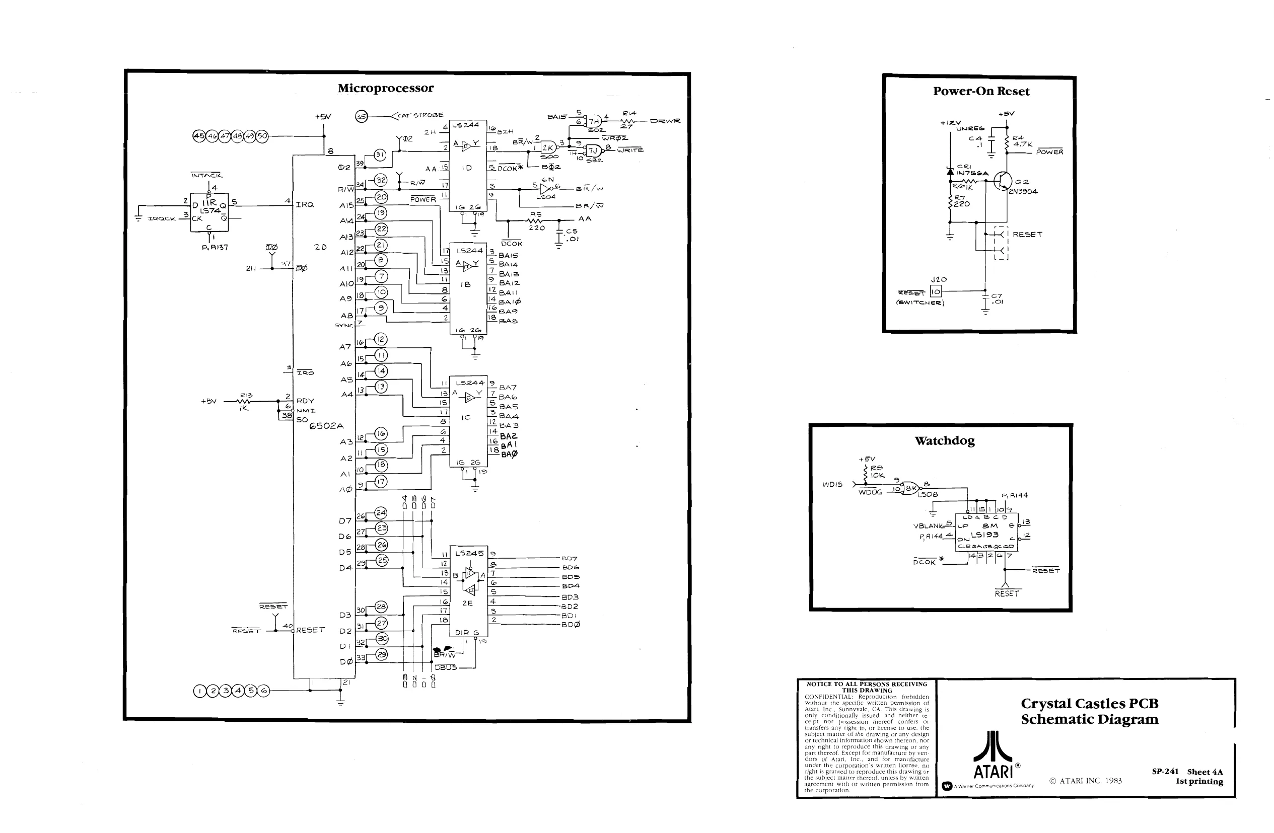
This page is a drawing, shown as the original scan.
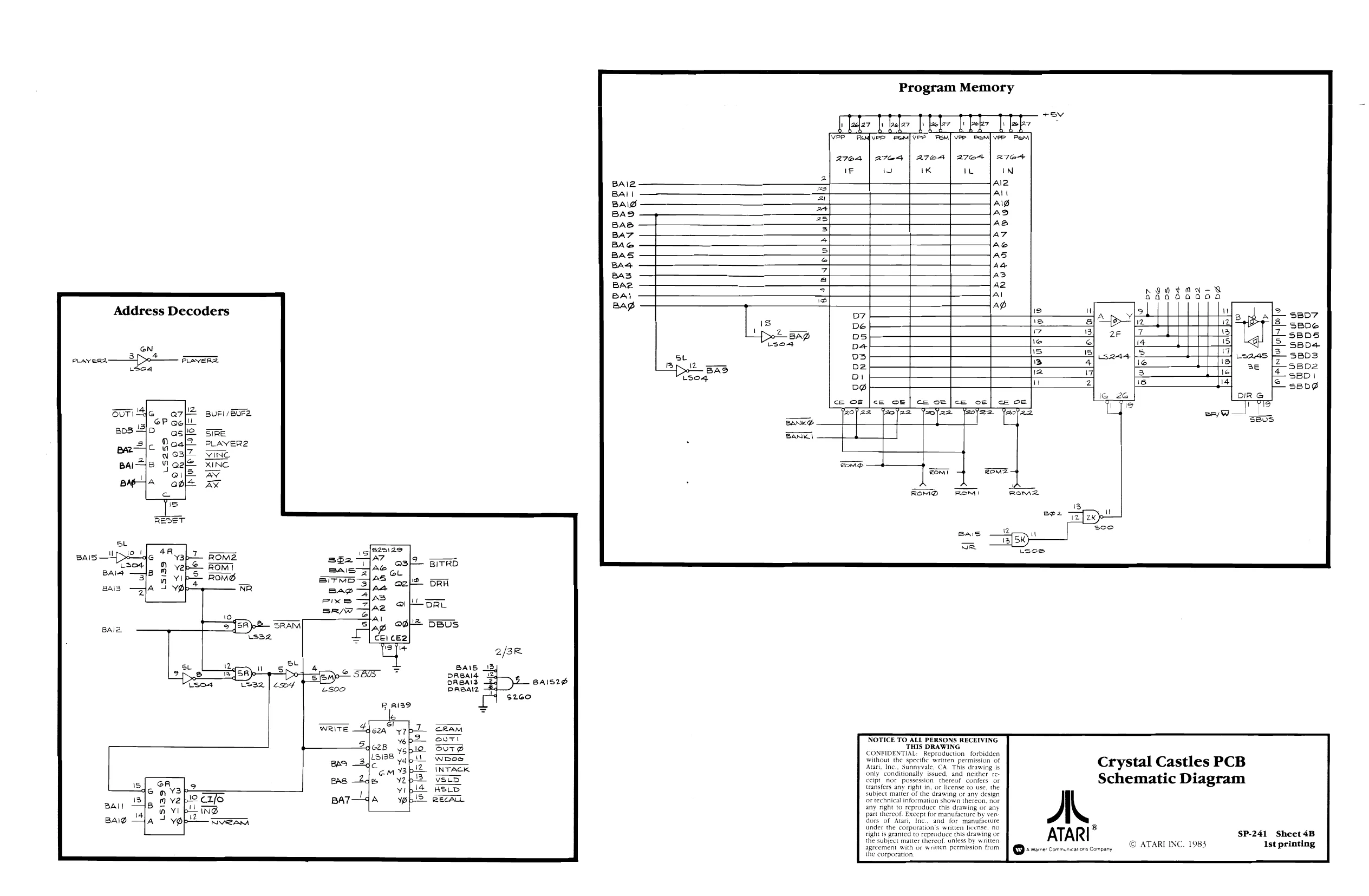
Address Decoders
PLAveR2:
a7}% avri B02 asl SRE eal? PLAYER2 w O32 Vine IS XING ae Ww ot AK
is[ezsi2e 862-47 i BITRD sass SITMB 5] oR sas ats exes SV aftoar
SBS BAIS 13. DRBAI4 Z ORBAIZ BAIS2¢d DRBAIZ
Program Memory
+ev Lee
84] o]sfo}o]a} uf ofS] 2] a]
NOTICE TO ALL PERSONS RECEIVING THIS DRAWING CONFIDENTIAL: Reproduction. forbidden without the specific written permission of Atari, Inc., Sunnyvale, CA. This drawing is only’ conditionally issued, and neither receipt_nor possession thereof confers oF transfers any right in, or license to use, the subject matter of the drawing or any design or technical information shown thereon, nor any right to reproduce this drawing or any
part thereof. Except for manufacture by ver
dors of Atari, Inc.. and for manufacture under the corporation's written license, 0 right is granted to reproduce this drawing or the subject matter thereof. unless by written agreement with or written permission from the corporation.
Crystal Castles PCB Schematic Diagram
A,
ATARI”
© ATARI INC. 1983 SP-241 Sheet 4B Ist printing
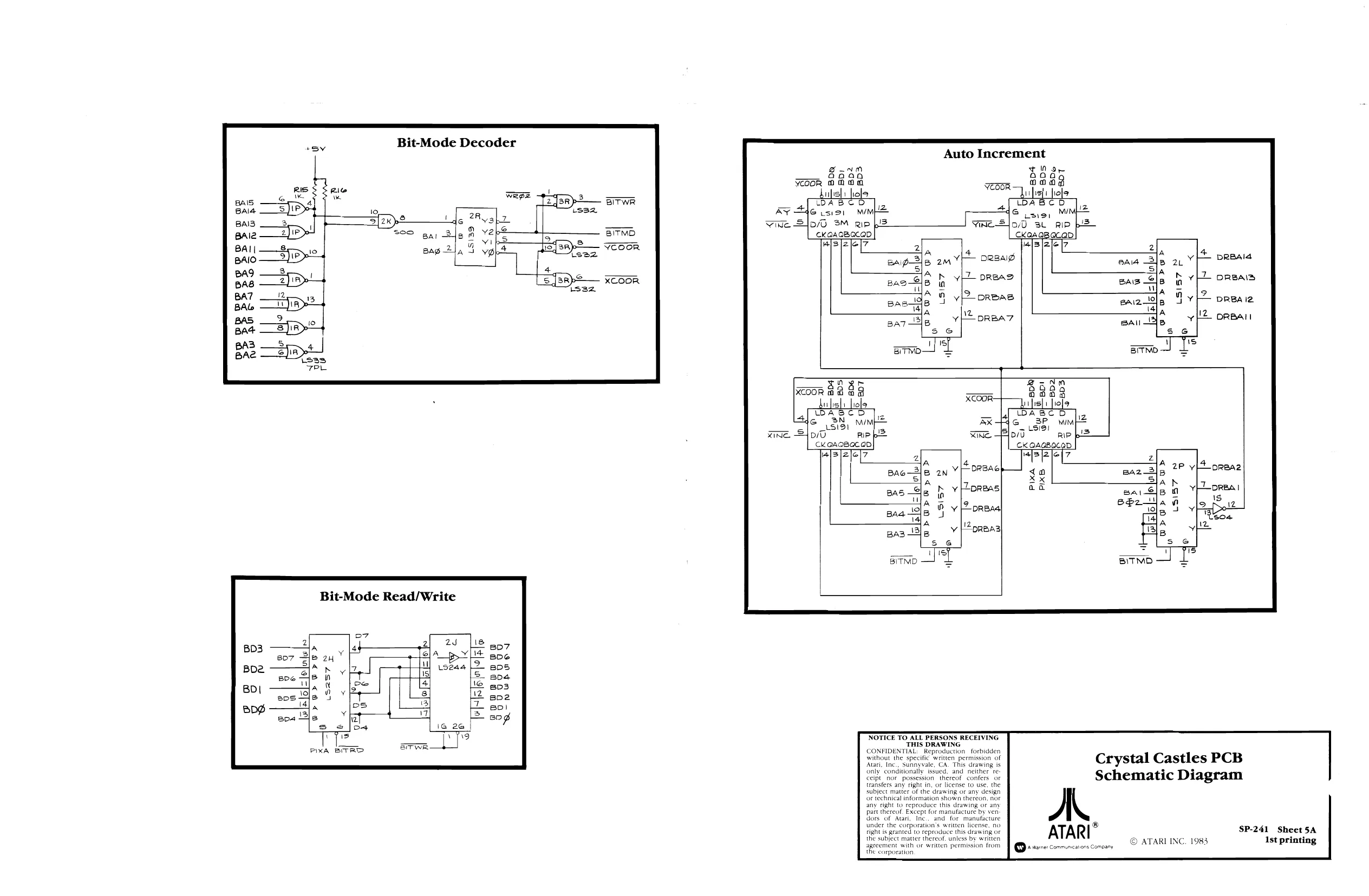
This page is a drawing, shown as the original scan.
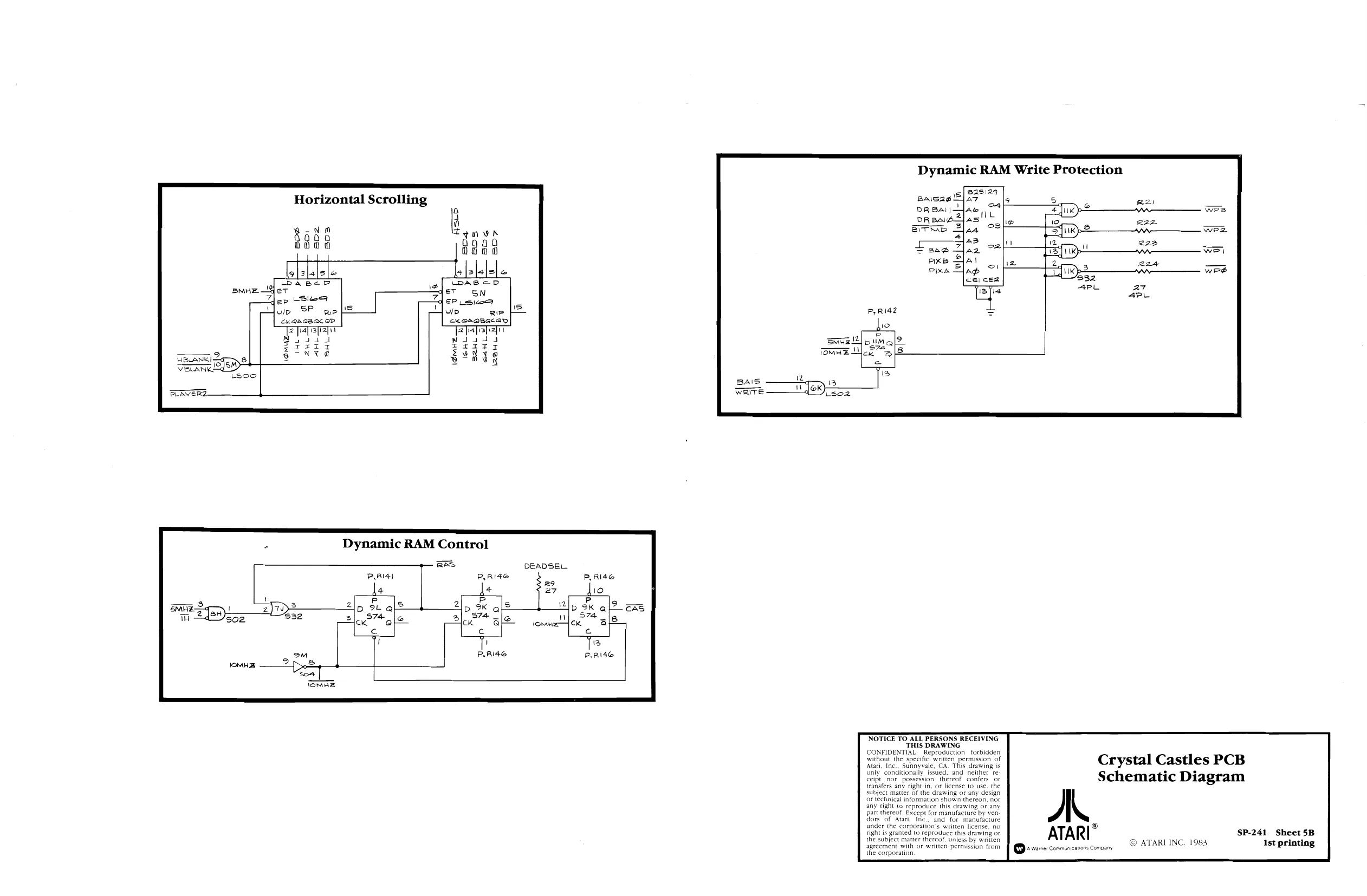
This page is a drawing, shown as the original scan.
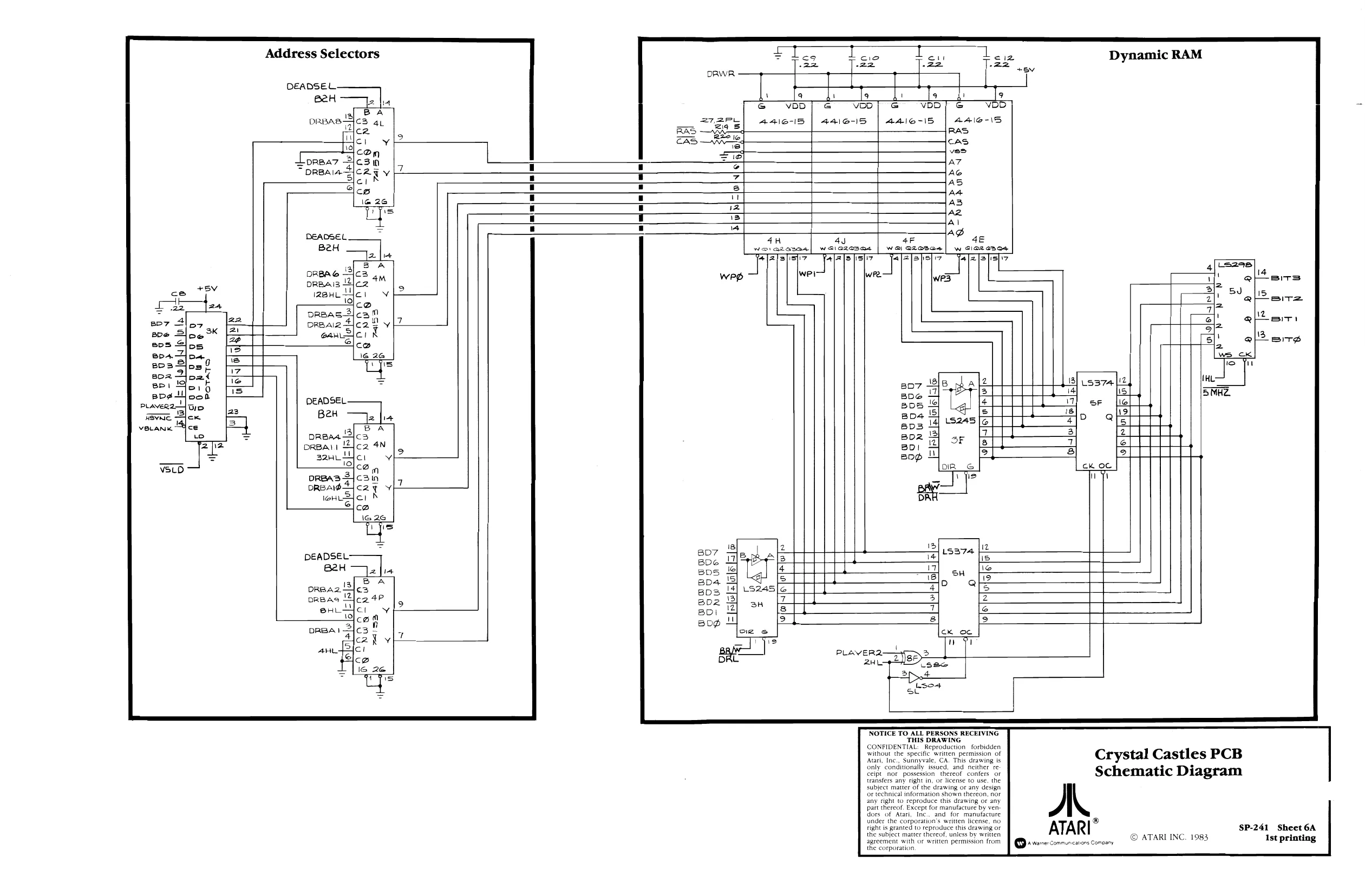
This page is a drawing, shown as the original scan.
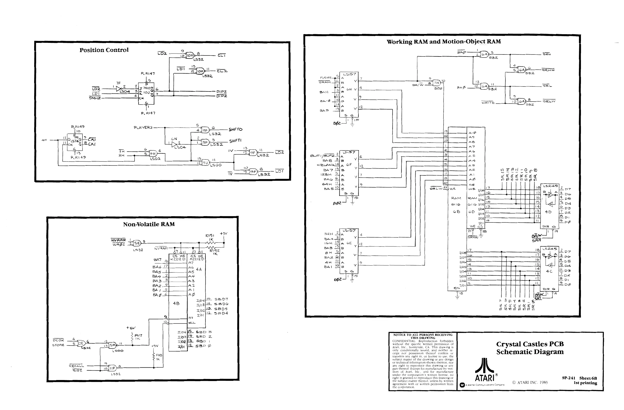
Non-Volatile RAM
NVRAM eis) +Y
1K
WaBZ =
HH tS WE] cS we *22i2D] K2212D Al Ab ne 4A
At ltd —4A2 Al Ag Rise wK
Working RAM and Motion-Object RAM
Grergprar Ae ag
ae
AT
Ae
AS
Aa
Az
Aa
Al Ae
TrU>T>R>Y
NOTICE TO ALL PERSONS RECEIVING ‘THIS DRAWING CONFIDENTIAL: Reproduction forbidden without the spectfic written permission of Atari, Inc., Sunnyvale, CA. This drawing is, only’ conditionally issued, and neither re ceipt nor possession thereof confers or transfers any right in, or license to use. the subject matier Of the drawing or any design nical information shown thereon, nor to reprowuce this drawing or any eof. Except for manufacture by ven. dors of Atari, Inc, and for manufacture under the corporation's writien license, no
right Is granted to reproduce this drawing OF
the subject matter thereof, unless by written agreement with or wittten permission from the corporation, WE veal
yor RAM og
elie wos}
A ATARI” + W217: Communications Comaae
Crystal Castles PCB Schematic Diagram
© ATARI INC. 1983 SP-241 Sheet 6B Ist printing
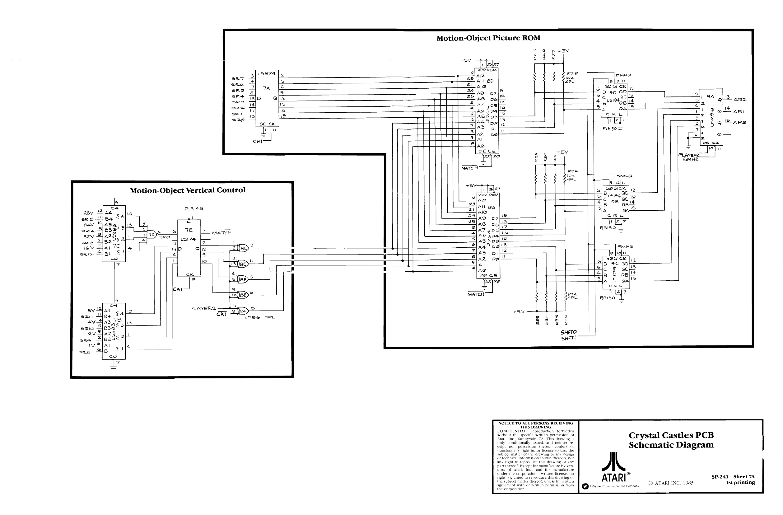
This page is a drawing, shown as the original scan.
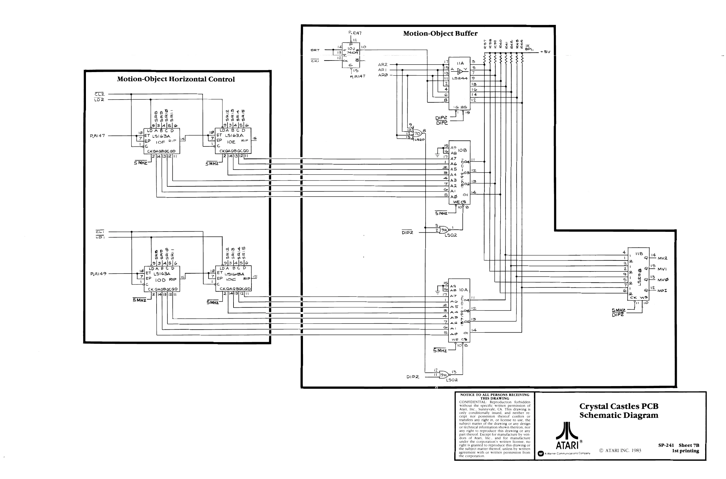
This page is a drawing, shown as the original scan.
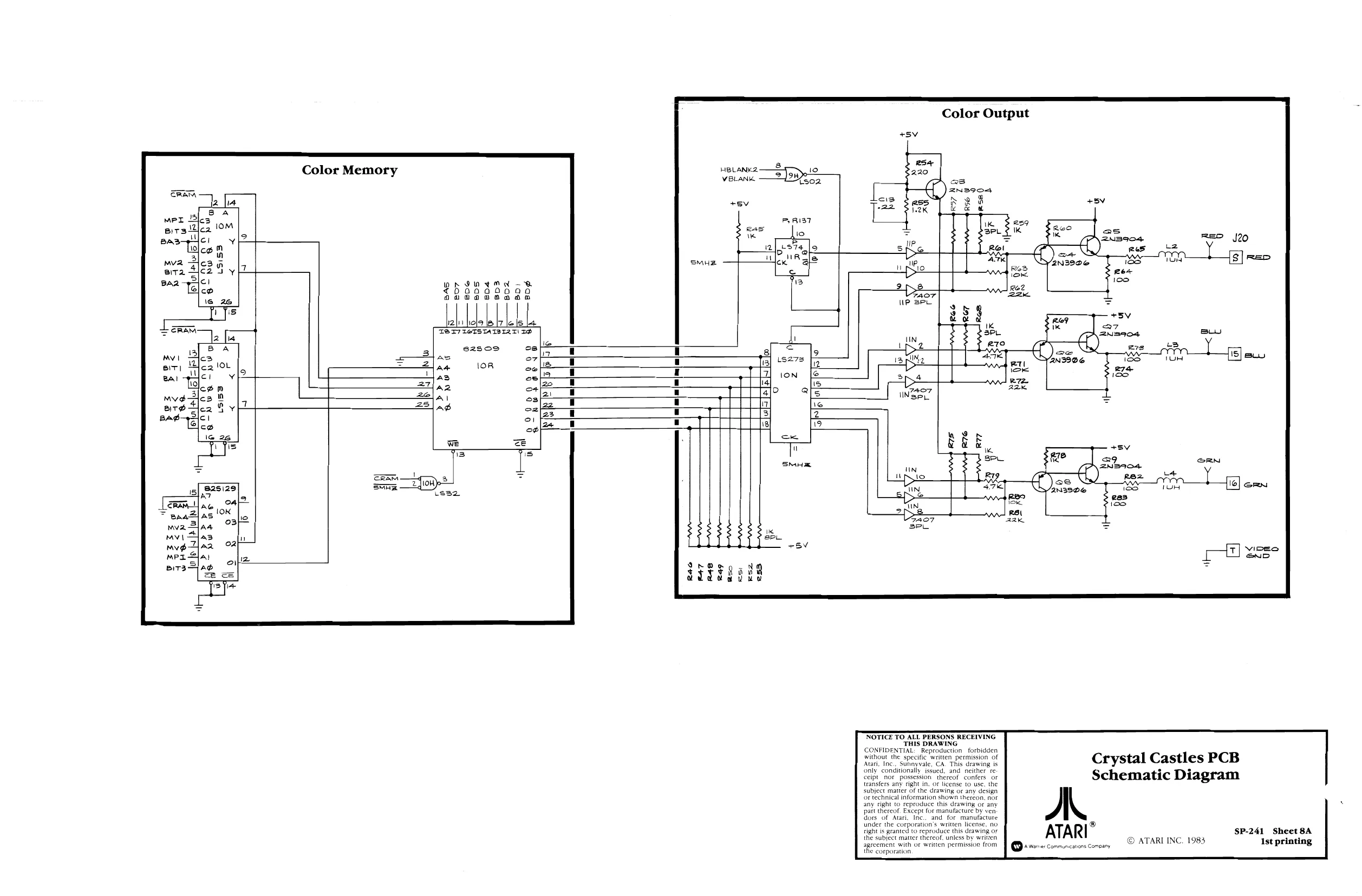
This page is a drawing, shown as the original scan.
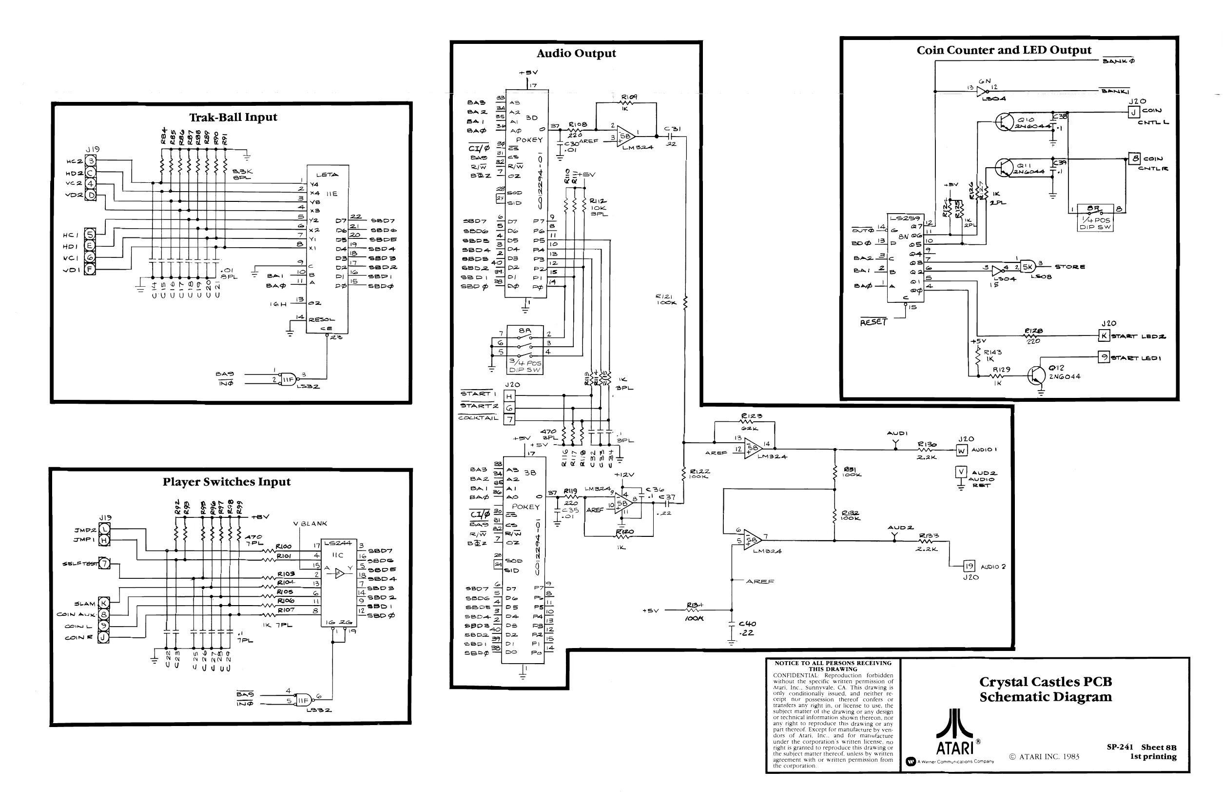
Trak-Ball Input
+ PREEIEEE:
Player Switches Input
Rico V BLANK
LSaae
zs uc
15]
S mn
Audio Output
START I
STARTZ
SSaeTAIL
Coin Counter and LED Output
GN BN 2 ara io JLO
J20
Ki|stamr Leo2
[SJerner vec O12 2NGO44
JLO Eizo Ww] Avi!
"NOTICE TO ALL PERSONS RECEIVING THIS DRAWING CONFIDEN’ Reproduction forbidden without the specific written permission of Atari, Inc., Sunnyvale, CA. This drawing is only conditionally issued, and neither re ceipt_ nor possession thereof confers or transfers any night in, or license to use, the subject matter of the drawing or any design or technical information shown thereon, nor any right t© reproduce this drawing or any
part thereof. Except for manufacture by ven right is granted to reproduce this drawing Or
dors of Atari, Inc. and for manufacture under the corporation's written license, no
the subject matter thereof, unless by written agreement with of written permission from the corporation, AyDio 2
J20
Crystal Castles PCB Schematic Diagram
A ATARI ® SP-241 Sheet 8B vere cummncnions conoany © ATARI INC, 1983 1st printing
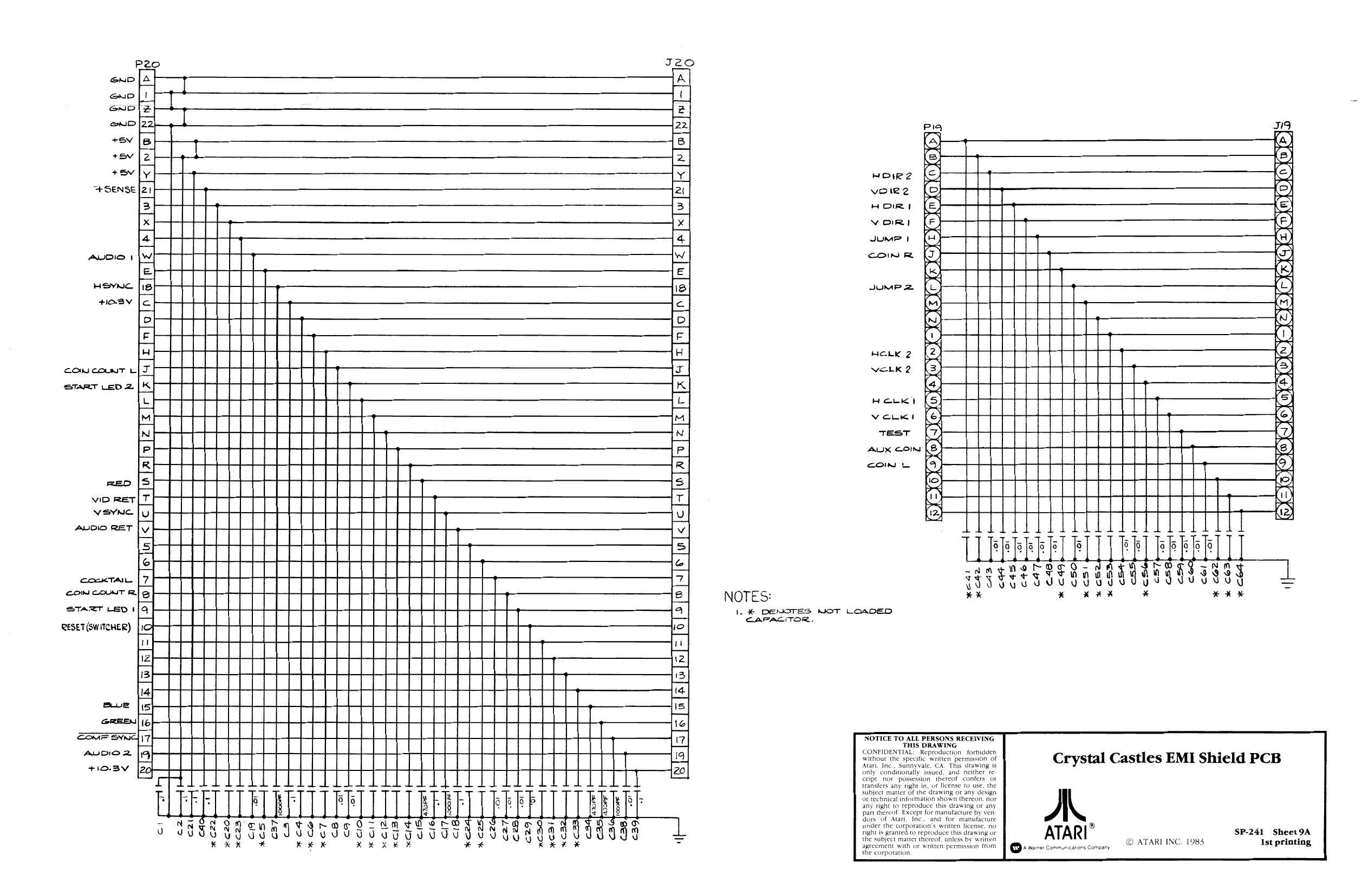
+eEvV
+ev
+ SENSE
AUDIO |
+1O3BV
CON COUNT L| START LEDZ
VID RET
VsYnc
AUDIO RET
CocKkTAIL.
CON COUNT R|
START LED!
RESET (SWITCHER)
cone ey AvoIC 2 +H1O.BV Gq N
PEEP PP BPEPEPEEDP ERS ~|> 2Jols Jejut<]e [a fu [alolz [zr [x jefe [nfole lele fe [e [= [eS ]< [eo
= [0 [2] jv feful< fe fa[v fal ]z |x
NOTES:
Tr iS
HOIRZ
voir2
HORI
vor)
JUMP 1 TN
r; AA
E}
CON R
14) Aa ie) SUMP 2 1G:
OS) LOS) HOLK 2
VELK 2 e) (
HoLK) Lory LD,
VvVouKs
Test
AUX COIN
con
- % DENOTES NOT LOADED CAPACITOR.
NOTICE TO ALL PERSONS RECEIVING THIS DRAWING CONFIDENTIAL: Reproduction forbidden without the specific written. permission of Atari, Inc, Sunnyvale, CA. This drawing is issued, and neither re ion thereof confers or transfers any right in, of license to use. the subject matter of the drawing or any design or technical information shown thereon, nor yy fight to reproduce this drawing or any part thereof. Except for manufacture by ven dors of Atari, Inc. and for manufacture under the corporation's written license, no
right is granted to reproduce this drawing oF
the subject matter thereof, unless by written agreement with oF written permission from the corporation
Crystal Castles EMI Shield PCB
A. ATARI” © ATARI INC. 1983 SP-241 Sheet9A Ist printing,
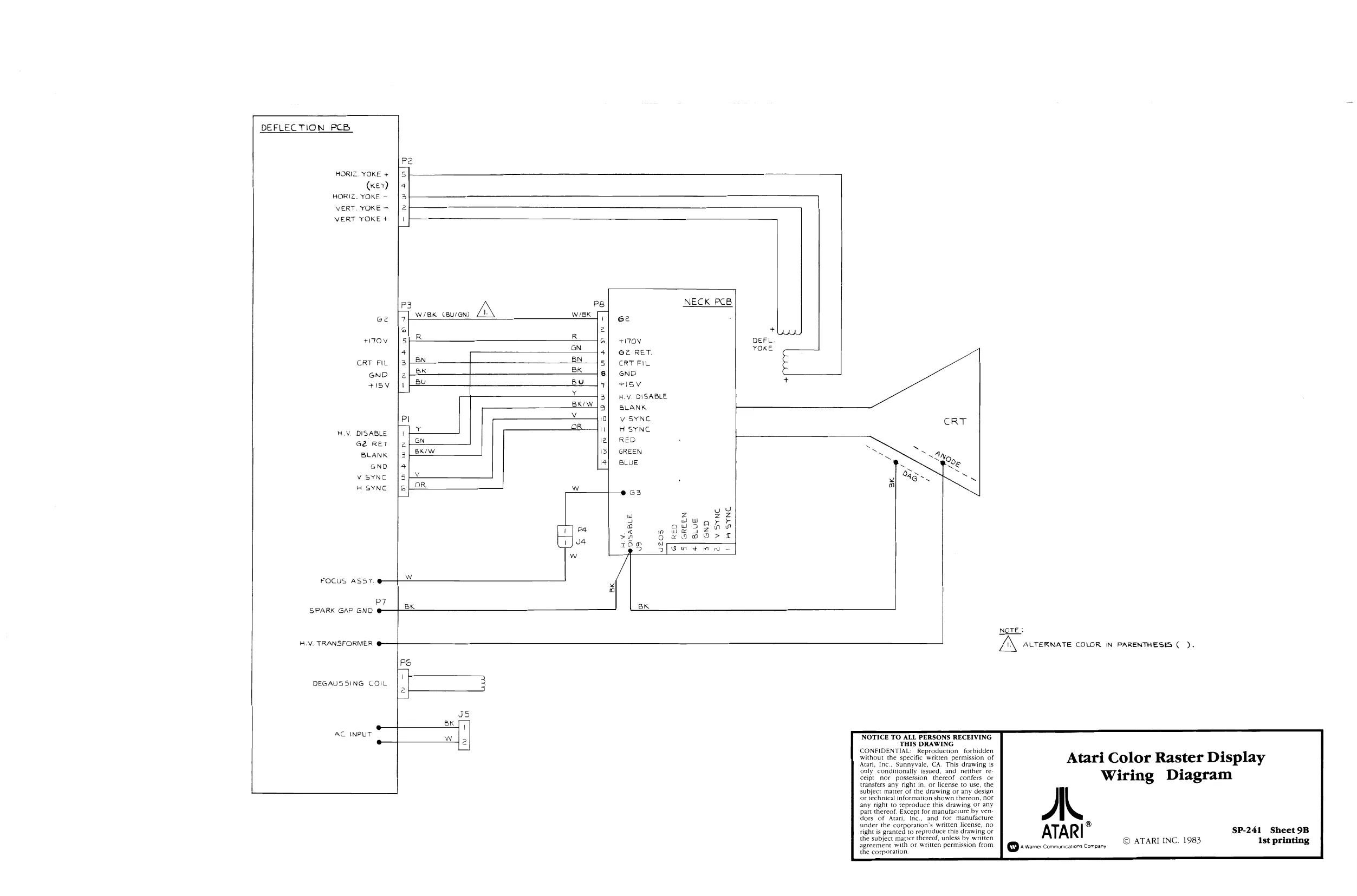
This page is a drawing, shown as the original scan.
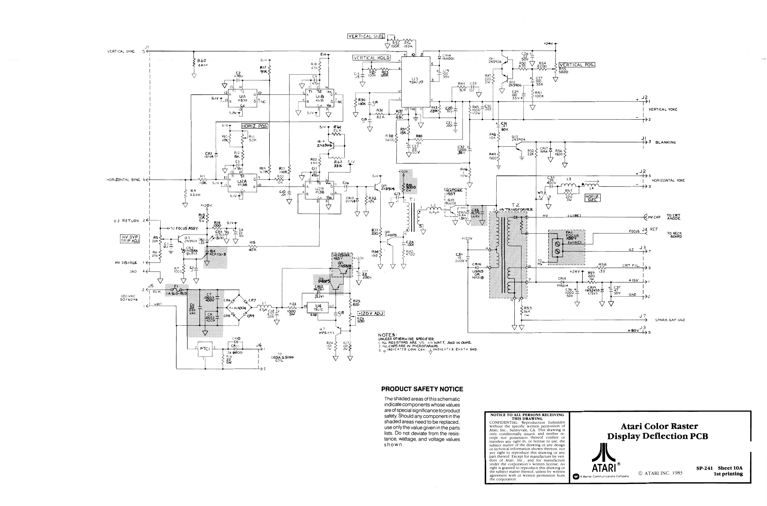
This page is a drawing, shown as the original scan.
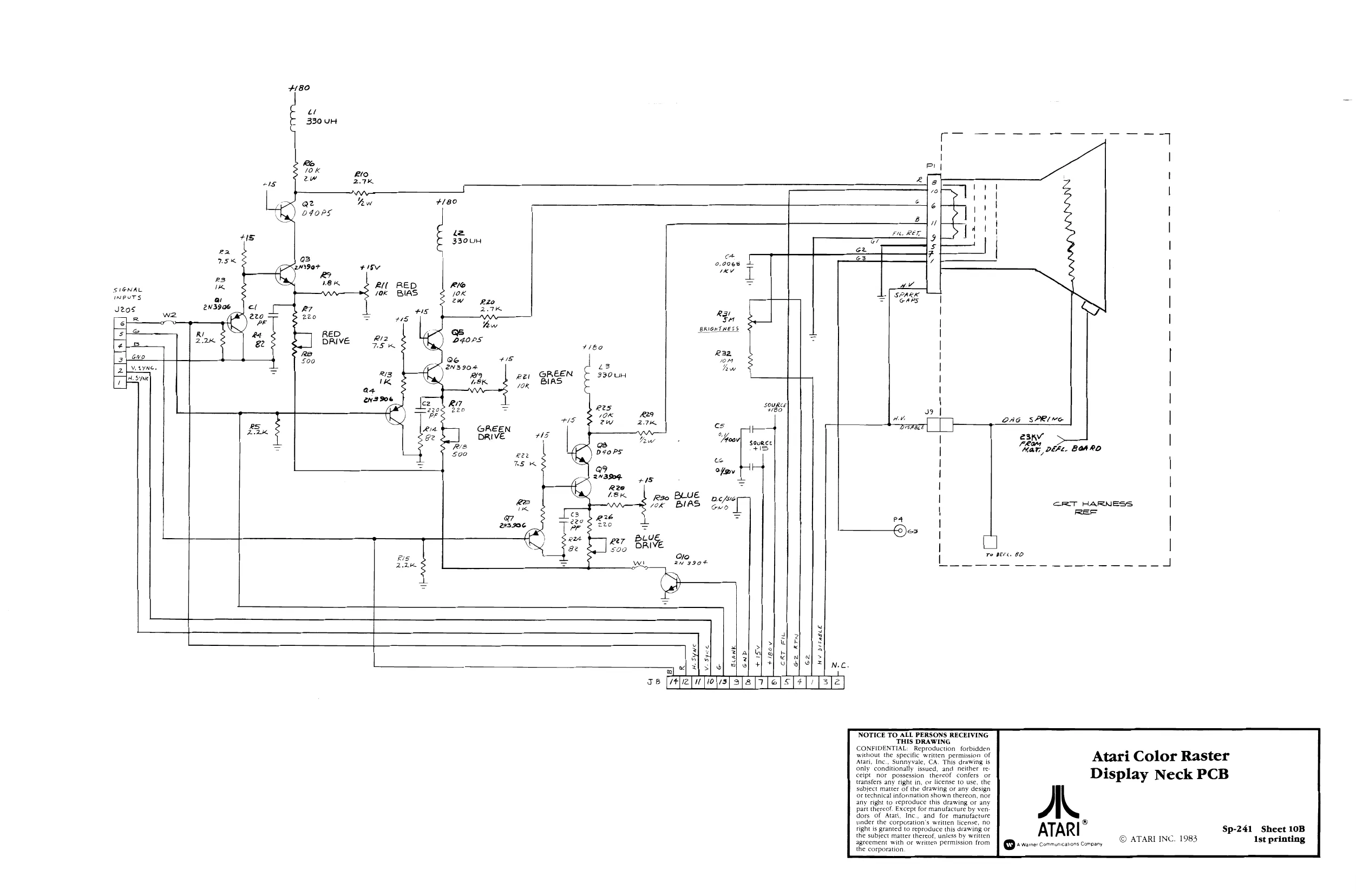
This page is a drawing, shown as the original scan.
This page is a drawing, shown as the original scan.