Lunar Lander DP-136-1st-02A
Lunar Lander (rev 2) (Atari, 1979) · Drawing Package · 1 pages · original scan
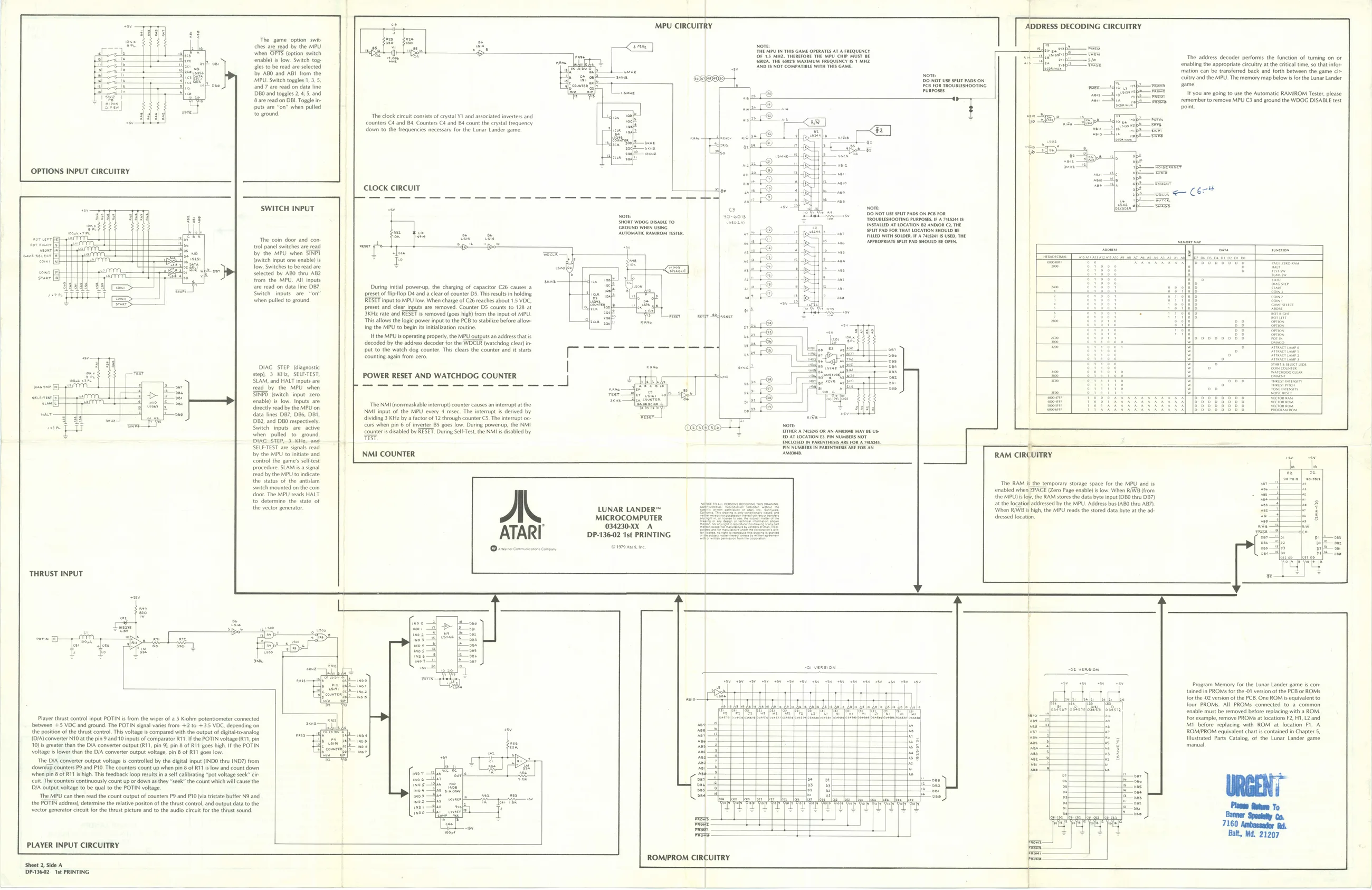
OPTIONS INPUT CIRCUITRY The game option swit ‘ches are read by the MPU when OPTS (option switch enable) is low. Switch togales to be read are selected by ABO and ABI from the
MPU. Switch toggles 1, 3.5,
dnd 7 ate read on data line DBO and toggles 2.4, 5, and 8 are read on DBI. Tose inputs are “on” when pulled to ground. MPU CIRCUITRY
mo [Eon pe
THRUST INPUT
Player thrust contol input POTIN is from the wiper of a5 K-ohm potentiometer connect
(DIA) converter N10 atthe pin 9 and 10 inputs of comparator RT. f the POTIN voltage (R11
- greater than the DIA converter output (R11, pin 9), pin 8 of RIT goes high. If the POTIN voltage is lower than the DIA converter output voltage, pin 8 of RTT goes low. ‘The D/A converter output voltage is controlled by the digital input (INDO thru IND7) from. ‘downiup counters P9 and P10, The counters count up when pin & of R11 i low and count down. ‘when pin 8 of R11 is high. This feedback loop results ina self cal
‘uit. The counters continuously count up or down as they “seek
DIA output voltage to be qual to the POTIN voltage rating “pot voltage seek
he count which wll cause
‘The MPU can then read the count output of counters P9 and P10 (via tristate buffer N9 and the POTIN address, determine the relative poston ofthe thrust contro, and output data to vector generator circuit forthe thrust picture and to the audio circuit forthe thrust sound
PLAYER INPUT CIRCUITRY between +5 VOC and ground. The POTIN signa varies from +2 to +35 VOC, depending on the position of the thrust control. This voltage is compared with the output of digita-to-analog SWITCH INPUT
The coin door and con: tuol panel switches are ead by the MPU when SINPI (switch input one enable) is low. Switches to be read are selected by ABO thru ABZ from the MPU. All inputs ate read on data line O87, Switch inputs are “on” ‘when pulled to ground.
DIAG STEP (diagnostic step). 3 KHz, SELFTEST, SLAM, and HALT inputs are fead_by the MPU. when SINPD (switch input zero tenable) is low. Inputs are
directly read by the MPU on
data lines D87, DB6, DBI, 1DB2, and DBO respectively Switch inputs are active ‘when pulled to. ground, DIAG: STEP, 3 KHe,-and SELF-TEST are signals read by the MPU to initiate and control the game's setest procedure. SLAM isa signal
read by the MPU to indicate
the status of the antslam
switch mounted on the coin
‘door. The MPU reads HALT to determine the state of the vector generator
ted The clock circuit consists of crystal YI and associated inverters and ‘counters C4 and B4. Counters C4 and 84 count the crystal frequency ‘down to the frequencies necessary forthe Lunar Lander game.
CLOCK CIRCUIT OF ts mine. THERE {THe MPU IN THIS GAME OPERATES AT A FREQUENCY THE MPO cle MUST BE \UMFREQUENCY 181 HZ ‘ADDRESS DECODING CIRCUITRY
DO Nor USE sru PADS Ow Peo YOR TROUBLESHOOTING
SHORT woos DIsAnLE TO GROUND WHEN USING
During inital powerup, the charging of capacitor C26 causes a preset of flip-flop D4 and a clear of counter DS. This results in holding RESET input to MPU low. When charge of C26 reaches about 15 VOC, preset and clear inputs are removed, Counter D5 counts to 128 at 3KHz rate and RESET is removed (goes high) from the input of MPU, ‘This allows the logic power input tothe PCB to stabilize before allow: Ing the MPU to begin is initialization routine. the MPU i operating properly, the MPU outputs an address that is decoded by the address decoder forthe WDCLR (watchdog cleat) input 0 the watch dog counter. This clears the counter and it starts ‘counting again from zero,
POWER RESET AND WATCHDOG COUNTER
‘The NMI (nonmaskable interrupt) counter causes an interrupt at the NMI input of the MPU every 4 msec. The interrupt is derived by dividing 3 KHz by a factor of 12 through counter C5. The interrupt oc ‘curs when pin 6 of inverter 85 goes low. During powerup, the NMI ‘counter is disabled by RESET. During Self-Test, the NMI is disabled by Test
NMI COUNTER ® TROUBLESHOOTING PURPOSES. FA 741824415. INSTALLED AT LOCATION 82 ANDVOR C2. THE SPLIT PAD FOR THAT LOCATION SHOULD BE
[APPROPRIATE SPLIT PAD SHOULD BE OFEN.
jaa
o\ale
LUNAR LANDER™ MICROCOMPUTER 034230-XX A DP-136-02 1st PRINTING
ia
the
the ED AT LOCATON €3 PIN NUMBERS NOT The address decoder performs the function of turning on or enabling the appropriate circuitry atthe critical time, so that infor mation can be transferred back and forth between the game ci culty and the MPU. The memory map below is forthe Lunar Lander same. IF you are going to use the Automatic RAMROM Tester, please remember to remove MPU C3 and ground the WOOG DISABLE test point
RAM CIRCUITRY
The RAM i the temporary storage space for the MPU. and is enabled when ZPAGE (Zero Page enable) slow. When RIWB (rom the MPU) s low, the RAM stores the data byte input (080 thru DB7) atthe location addressed by the MPU, Address bus (ABO theu AB7) When RIWE is high, the MPU reads the stored data byte atthe ad dressed locaton,
®
Sheet 2, Side A (DP:13602. 1st PRINTING Program Memory forthe Lunar Lander game is contained in PROMS forthe 01 version ofthe PCB oF ROMS for the 02 version ofthe PCB. One ROM is equivalent to four PROM. All PROMS connected to a common tenable must be removed before replacing with a ROM. For example, remove PROMSs at locations F2 H1, L2 and MI before replacing with ROM at location FI. A ROMIPROM equivalent charts contained in Chapter 5 IMustrated Parts Catalog, of the Lunar Lander game ‘manual