Meadows Lane
Meadows Lanes (Meadows Games, Inc., 1977) · Manual · 33 pages · 44 sections · original scan
This page carries no recoverable text. It is a drawing or a photograph. See the original scan.
MEADOWS LANES
MopeL ML-1
TABLE OF CORTENTS
t= INTRODUCTION
2- WARRANTY INFORMATION
3- SETUP AND CHECKOUT
4- GAME SEQUENCE
5- CABINET ENTRY
€- COIN ACCEPTOR
7~ ADJUSTHENTS /HAINTENANCE . COINS PER GAME
GAME TIMER
DISPLAY MONITOR
PCB REMOVAL
8- TROUBLE SHOOTING HINTS
TLLUSTRATIONS
FIGURE #2 COIN MECHANISM
FIGURE #2 LOGIC PCB
FIGURE #3 WIRE HARNESS
FIGURE #4 MONITOR MANUAL
ANTRODUCTION
MEADOWS LANES, a game of skill, Is a video bowling game. The
player must locate the "Bowler" tnside the gutters and then
bow! the ball either fast or slow, If the ball is not going
exactly where the player wants it to he can hook the bal}
either to the cight or to the left, but he can only hook the
ball one time. The instructions are printed on the video
screen and will provide the proper instructions for whatever
options that the operator has selected.
PRINTED CIRCUIT BOARDS: Contact the distributor from whom the game
was purchased for warranty repair and/or replacement information.
zuthorized service people, or any damage due to improper
handling or use shall void any existing warranty, Proper
procedures for removal and replacement, as outlined in
manual, must be adhered to.
DISPLAY MONITOR: Contact the distributor from whom the game was
purchesed for werranty repair and/or replacement information.
authorized people, or any damage due to improper handling
er use, shall void sny existing warranty.
‘ERT URNED TO THE FACTORY MUST HAVE RET ER AND TRAVEL FREIGHT PREPAID. PLEASE LIST SYMPTOMS PEDITE REPAIRS. ALL £te Rot TOE RIZATION R PROBLEMS
DOWS | RES SETUP AND Ct
When the game is received and unpacked, save 21] packing materials
in the event that it was damaged and must be returned. After reading
MCABINET ENTRY" section, proceed to inspect the interior of the cabinet
for loose or damaged connectors, wires, hardware, etc. If cverything
seems in satisfactory condition, plug the game in and play it as de-
scribed in the section ''GAME SEQUENCE". For cuestions about length
of play time, coins per geme, sound level, er anything relating to
picture image, see the section NADJUSTENTS/KAINTENANCE!.
co. NTROL_AND SWITCH FUNCTIONS
col Operator selectable:
\ coin, 25¢, per player
r player
selectable
time to bow) ball
to bowl ball
ructions enc starts the cane
layed on the left side
of the monitor aad the second player score is displayed on the right
side, When a two player game is finished the word "WIKNER" Ts written
under the player with the highest score. In case of a
“THE® Ts written across the how!
th, the monitor ts
scored,
Entry Into the MEADOWS LANES cabinet is at three points: the coin door,
the beck door, and the control panel.
COUN DOOR
The coin door is hinged to open from right to left giving access to
the following:
Coin Box Coin Mechanism Control Panel Wing Nuts
BACK DOOR
The back door tilts out from the top and lifts up for removal. This
allows access to the following:
Display Monitor Harness Logic PCB Sound PCB
CONTROL PANEL
To open the control pane) open the coin door first. Remove the two
wing nuts located up towards the control panel to the left and right
Finally, swing the control panel away from the cabinet. This will
give access to the following:
Cleaning Monitor/Inner Plexiglass Plexiglass Removal Speaker Start Switch Player Controls
COIN ACCEPTOR OPERATION, ADJUSTMENT AND MAUNTENANCE
SEE FIGURE 1
The detection and rejection of undesired or counterfeit coins are
determined by size (both thickness and diameter), weight and metallic
composition.
ic
The transfer cradie (#9) is used to test both the size end weight of
the coin. The coin must first pivot an 'undersize’ ‘ever (10) to
unlock the tran fer cradle and can be returned by actuating the wiper
operating tever (17). Oversize diameter coins will fail to pass
between the transfer cradle and the wiper and can be returned by
operating the wiper lever. Coins that are oversize in thickness will
fail to pass between the ma inet gate (11) end the main channel (5)
and will have to be dislod d by actuating the wiper eperati lever.
Underweight coins will fail to overcome the transfer credle counter-
weight and can be returned by operating the wiper lever. ° Q
A magnet is used to test the metallic composition of the coin. Highly
magnetic coins, such as steel or iron, will be retained by the magnet
and can be returned by actuating the wiper operating lever. Coins
having comparatively high magnetic properties will be slowed down by
the magnet and will drop off the rail short of the accept entrance and
will be returned. Coins having little or no magnetic properties, such
as brass or zinc, will pass through the magnetic field so fast they
will overshoot the accept entrance and will be returned.
ADJUSTMENT.
All coin acceptors Jeave the factory adjusted for maximum performance.
If, however, more critical adjustment is desired, or if the unit has
been disassembled for cleaning, the following adjustment procedure is
suggested.
KICKER AND SEPARATOR
a. Set the acceptor on a level surface with the back of the unit
facing you (the kicker and separator are on the back).
b. Loosen the screws holding the kicker (1) and the separator (3)
and move both the kicker (2) and the separator (4) as far to the right as they wid] go. Tighten the screws lightly.
c. Insert several test coins (both old and new) and note that
some are returned by striking the separator.
Loosen the separator screw and move the separator @ slight
amount to the left. Retighten the screw.
Insert the test coins again, and if some are still returned,
repeat Step d until ail coins are accepted.
Loosen the kicker screw and move the kicker @ slight amount to
the right.
Insert the test coins again and, if some of them are returned,
repeat Step Ff until all coins are accepted.
Be sure that both screws are tight efter the adjustments have
been made.
: SE OCH E TE eae
Set the acceptor with the front of the unit facing you in the
test position.
Turn the magnet gate adjuster (12) out (counter-clockwise)
until none of the coins will fit through.
With @ coin resting in the transfer cradle, turn the adjuster in
(clockwise) until the coin barely passes through the magnet gate.
Test this adjustment using several coins, and if any fail to pass
through the magnet gate, repeet Step ¢ until all coins are accepted.
Fix the gate acjustor in this position with a drop of glue or
Loctite, if necessary.
AAI NTEWANCE
on the environment in which the acceptor is used, periodic
preventative maintens nee should be performed.
The mainplate (5) may be cleaned with any liguid household clesner.
Thorough rinsing and drying are necessary to remove deposits and/or
film. Remove all metal particles from the net by guiding e screw-
driver along the edges of the magnet. Remove the transfer cradle and
nodersize lever and clean the bushings and pivot pins and re-aessemble.
Spray the entire unit lightly with WD-40, @ silicone lubricant.
The number of plays per coin is switch adjustable to either 1 coin per
or 2 coins per re} ame. See the i)lustration of the Logic PCB for
h details.
Length of time for pleyer ta bowl the ball can be-set for unlimited
time, 3 seconds or 5 seconds. See Logic PCB illustration for switch
details.
~ ”
a
pretence RK.
DISPLAY MONITOR, ADJUST
The displey monitor contains the following edjustments from left te
right:
Contrast: Adjustments for clear picture
tment te suit tocation
Adjustment if picture flips
ntal Hold: Adjustment if picture has disgonal Vines
or is distorted
For any maintenance see your ‘DISPLAY MONITOR MANUAL",
For access to display monitor see ‘Back Door'' section under "CABINET
ENTRY".
PCE_REKOVAL
Before removing PCB's, power cord should be disconnected. Note the
position of PCB to the connecter to ensure proper connection upon
replacement.
COMPONENTS OF GAME
BUTTONS | COIN SWITCH are normally closed. When pushed they are cpen.
The butions can be by-passed by pulling off one of the terminals.
Pace &
RNESS can be tasted by an ohm ter or continuity check
checked by visual Ten or continuity chec
OR can be checked by subst
a < # 2, = = CB, sound PCB & mon
RO PICTURE: Check if beck of picture tube is
fuses, power cord, end power outlet.
not Tit, air of monitor fs necessary.
If the tube is Vit, check scj ustments of brightness and c
Test continuity ef logic board pins #1 and #3
end pin £5 {video output). If all check out,
logic PCB or the monitor.
Check the edjusiment of the volume control on
Check the speaker, logic PCB, and TV monitor. er.
er.
itution of
itor should
is
ontrast.
the Sound PCB.
Lop Le a Zo) FUNCTION Lge | . an ne A i } NO Tine Limite 01.4 ed ee To Huwl Babe | { i 3B Séa. Trine Lime 4
|__| Bowe Pan 5 SEQ, Ti writ |} ! i
t vs j i | [Oba tl af re Bow ae |
i
COMPONENT SIDE
ena “4
, | |_— | | ~_orr | aS¢ / PLaver | | ~ Low | 50¢ /Peiyen | 7 | MEADOWS LANES [ | OPERATOR OPTIONS
ro j
COIN ACCEPTOR — EXPLODED
COIN FACE PLATE
FIGURE 4
MODEL XM501-10
CHASSIS 19VP111 XM701-10
23VP111
FILE vP12
MANUAL 68P65130A70-1 MOTOROLA
service manual
GENERAL INFORMATION
These models are transistorized monitors designed for the video game market. They are identical except for the CRT size. See V1 in Replacement Parts List.
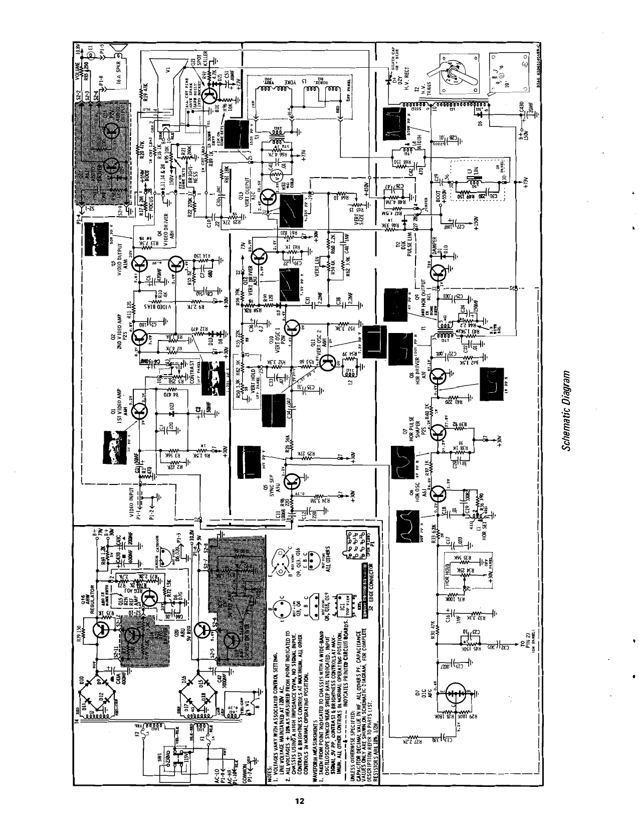
Circuitry includes four stages of video amplification, a two stage audio amplifier, sync and deflection circuits and a regulated power supply. An additional 5 volt 3 amp supply is included to power external logic systems. The picture tube is a 114 degree deflection CRT with implosion protection. Composite video is fed to the monitor through a connector mounted on the rear of the chassis.
Rear Horizontal panel controls include Hold, Vertical Hold, Contrast, Brightness, Volume and width controls. Additional service controls are mounted on the plated circuit panel, and are accessible from the rear of the chassis.
MOTOROLA INC.
PART NO. 68P65130A70-1 3-75 The chassis utilizes plug-in etched panel construction with components mounted on the top side and plated wiring on the bottom. Component reference numbers and circuit legend are printed on the board to aid in servicing. Horizontal, vertical output and regulator transistors are mounted ‘on the chassis base which also serves as a heat sink and CRT support.
ELECTRICAL SPECIFICATIONS
Power Rating: 110 watts nominal. 50 watts without 5 volt supply.
Source: 120/240V AC at 50/60Hz Switch selected.
Video Input: 0.5 to 2.5 volts composite PP (sync negative).
Audio Output: 5 watts peak
Display Products
PRICE 80 CENTS COPYRIGHT 1974 BY MOTOROLA INC. FILE VP12
DISPLAY PRODUCTS
CHASSIS
19VP111 23VP111
MODELS
XM501-10 XM701-10
NO WORK SHOULD BE ATTEMPTED ON ANY EXPOSED MONITOR CHASSIS BY ANYONE NOT FAMILIAR WITH SERVICING PROCEDURES AND PRECAUTIONS.
TABLE OF CONTENTS
CHASSIS PARTS LOCATION CHASSIS SCHEMATIC DIAGRAM REPLACEMENT PARTS LIST 2... eee ee ee SAFETY WARNING SERVICE NOTES THEORY OF OPERATION
CAROL STREAM, ILLINOSS 60187
PRINTED IN US.A.
SAFETY WARNING
- SAFETY PROCEDURES should be developed by habit so that when the technician is rushed with repair work, he automatically takes precautions.
- A GOOD PRACTICE, when working on any unit, is to first ground the chassis and to use only one hand when testing circuitry. This will avoid the possibility of carelessly putting one hand on chassis or ground and the other on an electrical connection which could cause a severe electrical shock.
- Extreme care should be used in HANDLING THE PICTURE TUBE as rough handling may cause it to implode due to atmospheric pressure (14.7 Ibs. per sq. in). Do not nick or scratch glass or subject it to any undue pressure in removal or installation. When handling, safety goggles and heavy gloves should be worn for protection. Discharge picture tube by shorting the anode connection to chassis ground (not cabinet or other mounting parts). When discharging, go from ground to anode or use a well insulated piece of wire. When servicing or repairing the monitor, if the cathode ray tube is replaced by a type of tube other than that specified under the Motorola Part Number as original equipment in this Service Manual, then avoid prolonged exposure at close range to unshielded areas of the cathode ray tube. Possible danger of personal injury from unnecessary exposure to X-ray radiation may result.
4, An ISOLATION TRANSFORMER should always be used during the servicing of a unit whose chassis is connected to one side of the power line. Use a transformer of adequate power rating as this protects the serviceman from accidents resulting in personal injury from electrical shocks. It will also protect the chassis and its components from being damaged by accidental shorts of the circuitry that may be inadvertently introduced during the service operation.
- Always REPLACE PROTECTIVE DEVICES, such as fishpaper, isolation resistors and capacitors and shields after working on the unit.
- If the HIGH VOLTAGE is adjustable, it should always be ADJUSTED to the level recommended by the manufacturer. If the voltage is increased above the normal setting, exposure to unnecessary X-ray radiation could result. High voltage can accurately be measured with a high voltage meter connected from the anode lead to chassis.
- BEFORE RETURNING A SERVICED UNIT, the service technician must thoroughly test the unit to be certain that it is completely safe to operate without danger of electrical shock. DO NOT USE A LINE ISOLATION TRANSFORMER WHEN MAKING THIS TEST.
In addition to practicing the basic and fundamental electrical safety rules, the following test, which is related to the minimum safety requirements of the Underwriters Laboratories should be performed by the service technician before any unit which has been serviced is returned.
ar 1000 OHM/VOLT (OR HIGHER) AC VOLTMETER NOTES. 1 REPEAT EACH CHECK WITH THE LINE CORD REVERSED 1N THE POWER OUTLET. 2 METER READING MUST NOT EXCEED 7-1/2 VOLTS AC. "MOT" LEAD OF METER TO EACH EXPOSED PART OF CABINET... (AS WELL AS THE CABINET. |] GROUND LEAD OF METER TO ANY CARTH ‘GROUND SUCH AS COLD WATER PIPE a.
1500 OHM 10 WATT RESISTOR INSULATOR
Voltmeter Hook-up for Safety Check
A 1000 ohm per volt AC voltmeter is prepared by shunting it with a 1500 ohm, 10 watt resistor. The safety test is made by contacting one meter probe to any portion of the unit exposed to the operator such as the cabinet trim, hardware, controls, knobs, etc., whiie the other probe is held in contact with a good “earth” ground such as a cold water pipe.
The AC voltage indicated by the meter may not exceed 7% volts. A reading exceeding 7% volts indicates that a potentially dangerous leakage path exists between the exposed portion of the unit and “earth” ground, Such a unit represents a potentially serious shock hazard to the operator.
The above test should be repeated with the power plug reversed, when applicable.
NEVER RETURN A MONITOR which does not pass the safety test until the fault has been located and corrected.
THEORY OF OPERATION CRT DISPLAY MOOULE - COMPOSITE VIDEO SYSTEM VP12
COMPOSITE BRIGHTNESS
VIDEO VIOEO AMP INPUT —+]
VERTICAL HIGH osc VOLTAGE
a SUPPLY
VERTICAL OUTPUT SYNC SEPARATOR
HORIZONTAL OSCILLATOR HORIZONTAL OUTPUT HORIZONTAL AFC
15,500 - 16,000Hz
Block Diagram
POWER SUPPLY
The power supply is a transformer operated, full wave, regulated supply which maintains constant output voltage with input variations of +15%. A switch (SW1) is provided to allow operation from 115/230 volts, 50/60Hz. The regulator is a series Pass circuit. Q16 is the series pass transistor, Q.15 the reference amplifier and Q14 the output driver.
The output voltage of the regulator appears at the emitter of Q16. This voltage is divided between R71, R74 and R73. The voltage appearing on the arm of potentiometer R74 is a reference input to the base of Q15.
A temperature conpensated zener diode (D6) is used to establish a fixed reference voltage at the emitter of Q15. R72 provides a bias current for D6, establishing its operating point.
An increase in output voltage will result in an increase of voltage at the base of 15. Since the emitter of Q15 is held at a fixed reference voltage, the change in base voltage will turn Q15 on harder, reducing its collector voltage. This reduces forward bias for Q14 resulting in less emitter current and less base current for Q16. Q16 will conduct less, lowering the output voltage.
R79 provides a shunt current path for.Q.16 allowing it to run coolet, improving reliability. C44 is.an RF noise filter.
A fixed, regulated 5V DC supply is used to power circuits external from the monitor. Its operation is similar to the 73V regulator except for the reference amplifier which is contained in the IC package.
a a 3 1ST VIDEO AMP. MME VIDEO OUTPUT ViDeo INPUT
| Priges= | Cy’ | . | x |
“pra =P in xs
| pie. | Ez) | wy | FF | ICR LAE yy 2 |
= 0g Ro 4 4 R18 IK, pa — « VIDEO DRIVER ‘aa } ES ax
VIDEO AMPLIFIER
The video amplifier has four stages incorporating devices Q1, Q2, Q3 and Q4. The first stage, Q1, functions as an emitter follower. The low output impedance of the first stage permits use of a low resistance contrast control which furnishes flat video response over its entire range without the need for compensation. The collector output of Q1 is used to drive the sync separator. C3 provides high frequency roll off to limit the collector output to the bandwidth required to pass synchronization signals. Q2 is a common emitter stage and is directly coupled to Q4. Q3 and Q4 are connected in a cascode configuration, This common emitter-common base connection greatly reduces the effect of Miller capacity compared with a conventional single transistor video output stage. C6 provides a ground for video at the base of Q3, the grounded base transistor of the video output cascode pair. Diodes D13 and D8 provide temperature compensation for the video output stages, and diode D23. Protects Q1 from transients.
The video bias control R10, is used to set the quiescent collector voltage of Q3. C5, C7, C8 and R15 are used for high frequency compensation. The video amplifier output is direct coupled to the control grid of the CRT through R18 which is used to isolate Q3 from transients that may occur as a result of CRT arcing.
PAR SYNC SEP Liev
| SYNC SEPARATOR | FROM | Cllyy, | R98 220 |
The sync separator employs a single stage, Q5, to recover sync a woe!
from the composite video signal. A single stage sync separator is adequate due to the high impedance of the following stages. The video input to the sync separator is black positive. C11 is charged by the peak base current that flows when the positive peak of the input takes Q5 to saturation. This charge depends ‘on the peak to peak input to QS and thus makes the bias for Q5 track the amplitude of the input signal. As a result Q5 amplifies only the positive peaks of the input signa{. The initial bias current through R24 sets the clipping level. R98 is used for transient protection, REFERENCE HORIZ. SYNC PHASE DETECTOR A
The Phase Detector consists of two diodes in a keyed clamp circuit. Two inputs are required to generate the required BO output, one from the sync separator and one from the horizontal deflection system. The required output must be of OSC ON FREQ NO CORRECTION VOLTAGE DEVELOPED
the correct polarity and amplitude to correct phase differences c OSC SLOW,POS
| between the input sync and the horizontal time base. The | 0 | CORRECTION VOLTAGE |
horizontal collector pulse is integrated into a sawtooth by R45.
| and C15. During syne time both diodes in D7 conduct, | 0 | OSC FAST,NEG |
shorting C15 to ground. o ~~ CORRECTION VOLTAGE
The sawtooth on C15 is thus clamped to ground at sync time. If the horizontal time base is in phase with the syne, the sync pulse will occur when the sawtooth is passing through its AC axis and the net charge on C15 will be zero. (Figure B). If the horizontal time base is lagging the sync, the sawtooth on C15 will be clamped to ground at a point negative from the AC axis, This will result in a positive DC charge on C15. (Figure C). This is the correct polarity to cause the horizontal oscillator to speed up to correct the phase lag.
Likewise, if the horizontal time base is leading the sync, the sawtooth on C15 will be clamped at a point positive from its AC axis, resulting in a net negative charge on C15 which is the required polarity to slow the horizontal oscillator (Figure D). R30, C17, C16 and R32 comprise the phase detector filter. The bandpass of this filter is chosen to provide correction of horizontal oscillator phase without ringing or hunting. Capacitor C23 times the phase detector for correct centering of the picture on the raster.
vP12 sync Input HORIZONTAL OSCILLATOR R27 22K D7 PHASE Q6 is employed in a modified type of recto Hartley oscillator. The operating frequency of this oscillator is sensitive to its base input voltage. This permits control by the output of the phase detector and also by the setting of the horizontal hoid control, R34. The horizontal hold range is set by adjustment of the core of L1.
PULSE SHAPER & HORIZONTAL DRIVER
Q7 is used as a buffer stage between the horizontal oscillator and horizontal driver. It provides isolation for the horizontal oscillator as well as a low impedance drive for the horizontal driver. R38 and C20 form a time constant which shapes the oscillator output to the required duty cycle (approximately 50%), to drive the horizontal output circuitry, The horizontal driver stage, Q8 operates as a switch to drive the horizontal output transistor through T1. Because of the low impedance drive and fast switching times furnished by Q7, very little power is dissipated in Q8. C21 and R42 provide damping to suppress ringing of the primary of T2 when Q8 goes into cutoff.
Tocet Nt HORIZONTAL OUTPUT ANODE suv ReC The secondary of T1 provides the required low drive @ . impedance for Q9. R44 and C24 form a time constant HOR OUTPUT for fast turn-off of the base of Q9, QQ operates as a switch which, once each horizontal period, connects the supply voltage across the parallel combination of the v horizontal deflection yoke and the primary of T2. The required sawtooth of deflection current through the horizontal yoke is formed by the L-R time constant of the yoke and output transformer primary. The horizontal retrace pulse charges C27 through D2 to provide operating voltage for G2 of the CRT. Momentary transients at the collector of Q9, should +o
they occur, are limited to the voltage on C27 since D2 ay ball Teo
will conduct if the collector voltage exceeds this value. = The damper diode, D1, conducts during the period between retrace and turn on of Q9, C28 is the retrace tuning capacitor. C29 blocks DC from the deflection yoke. L3 is a magnetically biased linearity coil which shapes deflection current for optimum trace linearity. L4 is a series width control. C31 and R49, C42 and R68 are damping network components for the linearity and width controls. C43D is charged through D5 developing the video supply voltage. f VERT BLANKING
oan
Syne from the collector of Q5 is integrated by R26 and C35, Q10 and Q11 are connected as a regenerative switch. The series combination of C37 and C38 charges through R58, R56 and D3 until Q10 turns on. This occurs when the emitter of Q10 exceeds its base voltage and causes current to flow into the base of Q11, turning that device on. When Q10 and Q11 conduct,
C37 and C38 are discharged to nearly zero. Q10 and Q11 then shut off and the cycle repeats. The setting of R82 determines the repetition rate of the charge and discharge of C37 and C38. The waveform generated is a positive going ramp or sawtooth with a fast retrace to zero. D3 provides a small incremental voltage above ground to overcome the forward sawtooth to alow impedance drive for Q13,
T3 matches the collector of Q13 to the vertical yoke. When Q13 is cut off during vertical-retrace, a high voltage pulse is develaped across the primary of T3. To limit this pulse to a safe value a varistor, R81, is connected across the primary. R66 and C41 provide damping to shape the collector pulse so it may be used for retrace blanking. Since ‘the primary impedance of T3 decreases with current, the degree to which the primary shunts the reflected.load impedance varies with collector current. This would result in severe vertical non-linearity unless some compensation is employed.
Resistors R59 and R6O couple the emitter voltage of NAY Irunerian pre-distortion of the drive sawtooth as shown in I VERTIEAL'DRIVE
Q13 to the junction of C37 and C38. Since this path As
| is resistive, the waveform coupled, back will be | : | C37, C38 |
integrated into a parabola by C38, This results in a
Figure C. This is done to compensate for the non 8;
| linear charging of C37 and C38 and the changing | \ | | VERT PARABOLA ADDED | |
| impedance of the primary. of T3. An additional | : | : | ! PARABOLA PULSE AND |
| feedback path through R62 and C40. serves to | i | VERTICAL SAWTOOTH ADDED |
optimize the drive waveshape for best linearity. c 1 TOGETHER, HENCE PRODUCING RETRACE BLANKING THE REQUIRED VERT DRIVING SIGNAL
Both vertical and horizontal retrace blanking are +15N Provided by positive pulses applied to the CRT 3 cathode. The collector pulse from the horizontal Raze output transistor is placed across R23 through R46. KF S The vertical collector voltage is differentiated by C30 +e to remove the sawtooth portion of the waveform, The remaining pulse appears across R23. The mixed vertical and horizontal pulses on R23 are coupled to Rl
the CRT cathode by C10. RO7 18K J
VERT AUDIO AMPLIFIER WN Q17 and Q18 form a DC coupled “switching tone burst amplifier’. An input signal biases Q17 on, in turn driving Q18 into conduction. When the signal is Pid removed both stages return to a quiescent mode. AuDiO
Coupling capacitor C50, diode D19 and resistor R88 INPUT
establish a bias voltage which is signal dependent. Volume control R85 sets the peak to peak level for the output stage. Lamp E1 serves to protect the speaker if the audio output transistor fails, it also protects the transistor should the speaker leads be shorted. Diode D22(on early models}polarizes the speaker insuring proper installation, if it is installed wrong, c50|+ AUDIO DRIVER
little or no audio will be developed. Q2i R95 10K SPOT SPOT KILLER +150V KILLER
Normally Q21 is not conducting and capacitor C51 is BRIGHTNESS
charged to the supply voltage. When the monitor is turned off, C51 discharges through R96 turning the TO transistor on. It in turn removes the positive potential CRT from the brightness contro! connecting the CRT CATHODE 200K cathode to ground, causing the tube to conduct hard, = SS +7 discharging the high voltage.
PANEL REMOVAL/INSTALLATION
To prevent damage to the board or foil when removing the circuit panel it may be necessary to pry up slowly, IN STAGES. araund the edges as.shown, Start at one corner and move all around the board keeping the screw driver tip against the chassis. When installing, apply pressure at the edges near the pins. Do not force down on the components.
CIRCUIT TRACING Component reference numbers are printed on top and bottom of the plug-in circuit board to facilitate circuit tracing. In addition, control names and board terminal numbers are also shown and are referenced on the chassis schematic diagram -in this manual. Transistor elements are identified as follows: E — emitter, B — base, and C — collector. COMPONENT REMOVAL Removing components from the etched board is facilitated by the fact that the circuitry (plating) appears on one side of the board only and the component leads are inserted straight through the holes and are not bent or crimped. It is recommended that a solder extracting gun be used to aid in component removal. An iron with a temperature controlled heating element would be desirable since it would reduce the possibility of damaging the board ‘due to over-heating. The nozzle of the soldering gun is inserted directly over the component lead and when sufficiently heated, the solder is drawn away leaving the lead free from the copper plating. This method is particularly suitable in removing multi-termina! components.
REGULATOR ADJUSTMENT
- Apply test signal to proper input. Signal should be of same amplitude and sync rate as when monitor is in service.
- Adjust vertical and horizontal oscillator controls until display is synced.
- Connect a DC digital voltmeter or other precision accuracy voltmeter to the emitter of the regulator output transistor, (or any 73 volt test point).
- Adjust the regulator control R74, on circuit board for an output of 73 volts. Do not “run” the regulator control through its range or damage to the monitor may result.
- When adjustment is complete, the AC line supply can be varied between 105 and 130 volts to check for proper regulator operation. With regulator operating properly, changes in display size should be negligible. HORIZONTAL OSCILLATOR ADJUSTMENT
| 1. Set | the | horizontal | hold |
potentiometer to mid-range (R34).
- Adjust core of horizontal hold coil L1 until the horizontal blanking lines are vertical.
| 3. Rotate | potentiometer | R34 |
through its full range: Display should go out of sync in each direction and hold in sync at the center of its range. Retouch L1 as necessary to center the hold range.
| VIDEO | AMPLIFIER | BIAS |
ADJUSTMENT Adjust video bias control R10 for 30 volts DC on collector of video output transistor Q3 with no signal input. Disconnect cable from video input jack if necessary to eliminate noise.
POWER TRANSISTOR REPLACEMENT When replacing any “plug-in” transistor, i.e., the horizontal or vertical output, please observe the following precautions: 1, The transistor sockets are not “Captive”, that is, the transistor mounting screws also secure the socket, When installing the transistor, the socket must be held in its proper location. This location is indicated by flanges on the socket which fit into the heat sink,
- When replacing the output transistors, silicone grease (Motorola Part No. 11M490487) should be applied evenly to both sides of the mica insulator.
- All transistor mounting screws must be tight before applying power to the receiver. This insures proper cooling and electrical connections. NON-COMPLIANCE WITH THESE INSTRUCTIONS CAN RESULT IN FAILURE OF THE TRANSISTOR AND/OR tTS RELATED COMPONENTS.
- Discharge CRT by shorting 2nd anode to ground. Remove CRT socket, yoke and 2nd anode lead.
- Remove CRT from chassis by removing four screws at corners, PANEL CONNECTOR CONTACT REMOVAL Contacts can be removed from the mulitpin panel connector by using extractor tool, Part No. 66P65173A47. Insert the tool over contact and seat fully. Tool will release contact. Pull contact out from wired side,
PIN 5 TO UNCODED SPEAKER TERMINAL
PIN 8 TO SPEAKER TERMINAL WITH PAINT DOT
Recommended Speaker Connection
CROSS SECTION OF CONNECTOR YELLOW PAINT DOT
CONTACT EXTRACTOR
Edge Connector Contact Removal vP12
oO” aa AUDID DRIVER CENTERING RINGS
VERT OUT
115/230. LINE SWITCH
VERT HORIZ Pt cont «BRITE, = HOLD. MOLD = VOLUME
Chassis Component Location Rear View
a8 aig 402518 pave tagr @ Pay ASG aupio ost 5V AEG DRIVER
were
Top View Circuit Side
Power, Audio Panel Component Location
vP12
| azo | a6 | PLUGIN | a13 | 13 |
R74 ag
| SV REG | T3VREG = 73V REG ADJ | MONITOR PANEL | ss | VERT OUT | ven our | HORIZ OUT |
TRA
D4 HV. RECT
‘T2 cK. TRANS:
| PLUG IN POWER | RIO | RES | it) | ut | RI7 | |
| AUDIO PANEL | swt | VIDEO BIAS | VERT SIZE | VERT LIN | HORIZ SET | Focus |
Chassis Component Location Top View
F200 FA RS R82 R34 R85 VE R21 CONTRAST BRIGHTNESS RT HOLD HORIZHOLD VOLUME
D10
D16 hc; IS 015 017 D18 012 D11 G20 O16 C51 D21 021 R66 Q13 C41 R81
Chassis Component Location Bottom View
D7 a7
AFC a6 HORIZ a8 11
PHASE HORIZ. PULSE HORIZ HORIZ
DET 03 OSC SHAPER ORIVE ORIVER
R74 73V
REG ADJ
TO CRT PIN3
G2
TO CRT PIN 2
a1 L3
HORIZ LIN
VIDEO oUuT ul HORIZ pa SET
D13 VIDEO i \ i ; i 7 PULSE DRIVE LIMITER CRT , | , : \2 # ‘ i R17 FIL PINS : < FOCUS
R10 VIDEO BIAS To 4] CRT PING ST AN SAEES AN : oa Focus
o. : +. GND i az a5 O10 TOCRT Q11 R65 RSG 1ST 2ND SYNC. -VERT PIN7 CATHODE VERT VERT VERT VIDEO SEP OSC-1 OSC-2 SIZE LIN
‘AMP ‘AMP Monitor Panel — Component Side
P12
Monitor Panel — Circuit Side
This page is a drawing, shown as the original scan.
REPLACEMENT PARTS LIST vera
PART NUMBER
| ‘REF.NO.| | PARTNUMBER | ‘DESCRIPTION | REF. NO. | | DESCRIPTION |
COILS & CHOKES
| ELECTRICAL PARTS | La | 24D68822A08 | HORIZ SET | |
| L2 | 24D68801A67 | COMPENSATING: 2000 uh | ||
| Ls | eee eats | HORIZ LINEARITY | ||
| a | 24V26000A74 | HOR IZ WIDTH: incls C42 & REB | ||
| MASO7AO | eG eee | us | 24D68523A15 | DEF LECTION YOKE |
| 1¥25017A02 | POWER, Audio Panel: complete: | TRANSISTORS | ||
| KTS65LM | a4 | 488137171 | 1st VIDEO: AGH | |
| a2 | 488137127 | 2nd VIDEO: P28 | ||
| a3 | 488134919 | VIDEO OUTPUT: AIM | ||
| a4 | 488137317 | VIDEO DRIVER: ABH |
CAPACITORS as 488137115 SYNC SEPERATOR: ASU
| a6 | 485137172 | HORIZ OSCILLATOR: A6J | ||||
| C1 | 23C65282A41 | 50 mf 5OV Lytic | a7 | 4885137127 | HORIZ PULSE SHAPER: P2S | |
| C2 | 23C65282A41 | 50 mf 50V Lytic | as | 488137093 | HORIZ DRIVER: ASF | |
| C3 | 218180010 | 220 pf 20% 100V XSF (Use 218132503) | 2-9 | 488137570 | HORIZ OUTPUT: B2L | ||
| ca | 23065282441 | 50 mf 50V Lytic | 10 | 488137173 | VERT OSCILLATOR (1): P2W | |
| cs | 218180898 | 180 pf 10% 500V X5F | Q-11 | 488137171 | VERT OSCILLATOR (2): A6H | |
| cs | 23810255478 | 470 mf 16V Lytic | 12 | 488137115 | VERT DRIVER: | ASU |
| C7 | 21S180C01 | 680 pf 10% S00V X5F | a13 | 488134900 | VERT OUTPUT: AIC | |
| cs | 218180885 | 560 pt 10% 500V X5F | at | 485134952 | REGULATOR ORIVER; A2Js | |
| C-10 | 8810191867 | .22 mf 10% 260V Polyester | O15 | 488137574 | REFERENCE AMP: B2N | |
| cn | 8S10191A54 — {0068 mt 10% 160V Polyester | Q-16 | 485137368 | REGULATOR: ASW | ||
| C12 | 218180D10 | 220 pf 20% 100V X5F (Use 21R 132503) | O-17 | 488137172 | AUDIO DRIVER: | AGS | |
| C13 | 218131625 | 330 pf 10% X5F | a-18 | 485137168 | AUDIO OUTPUT: P2V | |
| C15 | (218180041 | .0027 mf 10% 500V 25F (Use | Q-19 | 488137169 | 5V REGULATOR, Dri | |
| 21K 121699) | Q-20 | 488137344 | 5V REGULATOR: ABU | |||
| 1s | 2381022907 | 1.0 mf +40-20% 15V Lytic | 21 | 488137476 | SPOT KILLER: BIE |
(Use 23043280417)
| C17 | 8810191890 | 033 mf 10% 160V Polyester | CONTROLS | ||||
| C18 | 881029973 | 01 mi 10% 100V Poly carb | |||||
| 19 | 8S10299A74 | 0082 mf 10% 160V Poly carb | R | 18068222434 | CONTRAST: 250 Ohm | ||
| C20 | 8S10191B98 | —.01 mf 10% 250V Polyester | R-10 | 18066401444 = VIDEO BIAS: 4K | |||
| C21 | 218180851 | .001 mf 10% 500V XSF | R-17 | 18067858A12 | FOCUS: 2 meg | ||
| C22 | 8810191898 | 01 mf 10% 160V Polyester | R21 | 18D68222A35 | BRIGHTNESS: 200k | ||
| 23 | 2181800210 pf 10% N150 | R34 | 18D68222A37 | HORIZ HOLD: 25K | |||
| C24 | 23D85282A40 | 150 mf 10V Lytic | R-59 | 18D66401A44 | VERT LINEARITY: 4K | ||
| 6-25 | 218180851 | .091 mf 10% 500V XSF | ‘ | R65, | 18067671A18 | VERT SIZE: 15 Ohm | |
| c-26 | 8S10212853 | .47 mf 10% 630V Mtiz Poly | R74 | 17D65820A37 | REGULATOR ADJUST: 2K | ||
| C27 | 8810212411 | 1.0 mf 10% 630V Mtlz Poly | R82 | 18D68222A36 = VERT HOLD: 3K | |||
| C28 | 8S10571A06 = 01 mf $% 1200V Poly Prop Foil | RBS | 18068222434 = VOLUME: 250 Ohm | ||||
| 29 | 881057123 | 56 mf 10% 250V Prop Foil | RESISTORS | ||||
| ¢-30 | 8810191432 | 1047 mf 10% 250V Polyester | |||||
| c-31 | 21S180B87 | 220 pf 10% 500V XSF | R-1 | 68127633 | 470 10% 1/2W | ||
| C32 | 218180034 | 005 mf 20% 1KV Z5F (Use 218180031) J R-2 | 68125568 | 22K 10% 1/2W | |||
| c-33 | 8S10212A69 | -47 mf 10% 100V Mtiz Poly | R-3 | 68127541 | S6K 10% 1/2W | ||
| 34 | 8S10191A32 | —_.047 10% 250V Polyester | R-4 | 68127633 | 470 10% 1/2W | ||
| C35 | 8810191898 | _01 mf 10% 250V Polyester | R6 | 68128955 | 1500 10% 1W | ||
| c-36 | 23S10255A69 | 4.7 mf 100V Lytic | RA? | 68121847 | 4700 10% 1/2W | ||
| 37 | 8510212420 | 2.2 mf 10% 100V MtzI Poly | RS | 68122445 | 1800 10% 1/2W | ||
| C-38 | 8S10212A20 | 2.2 mf 10% 100V Mtiz Poly | Rg | 68119926 | 2700 10% 1/2W | ||
| ¢39 | 8S10191B67 | —.22 mf 10% 250V Polyester | R11 | 68128226 | 120 10% 1/2W | ||
| C40 | 8810212A10 | 1.0 mf 10% 100v Mtlz Poly (Use | R-12 | 68127633 | 470 10% 1/2W | ||
| 8S10191A46 | R-13, | 17810731A02 | 7500 5% Sw WW | ||||
| cal | 8510064A06 | .01 mf 10% 600V Mylar | R-14 | 68124797 | 150 10% 1/2W | ||
| ¢-42 | 213180471 _ 470 pf 10% S00V XSF | R-5 | 68127516 | 82 10% 1/2W | |||
| cag | 23C85807A47 | 400 mf/125V; 600 mf/SOV; | R-18 | a | Part of CRT socket assembly | ||
| 20 mf/200V Lytic | R19 | — | Part of CRT socket assembly | ||||
| C-44 | 218180E60 | .01 mf +80—20% 50V Z5V | R-20 | -—— | Part of CRT socket assembly | ||
| C47 | — *23C65807A52 | 5000 mf 20V Lytic | R22 | 68129296 | 270K 10% 1/2W | ||
| 50 | 23D65282A41 | 50 mi SOV Lytic | A-23 | 6810053C67 | 27K 5% 1/2W | ||
| 23810255843 © 40 mf 100V Lytic | R24 | 68127538 | 3.3 meg 10% 1/2W | ||||
| R25 | 6121300 | 27K 10% 1/2W | |||||
| DIODES & RECTIFIERS | R-26 | 68127541 | 56K 10% 1/2W | ||||
| Bae | Papi | (2200 10% 1/2W | |||||
| ba | 488134921 | it | 2 | 1 | 180k 10% 1/2W | ||
| 488134978 | DIODE, Silicon: D1K; Pulse Limiter | [R29 | 68125831 | 380k 10% 1/2W | |||
| 48D67120A11 | DIODE, Low Power | 8-30 | 6S125892 | 47K 10% 1/2W | |||
| 488137114 | RECTIFIER, H. V.: | Silicon; D2Y | B31 | 6S 125534 | 100K 10% 1/2w | ||
| D- | 488191 A05 | RECTIFIER, Silicon: 91A05 (Use | R32 | 68124506 | 9300 10% 1/2W | ||
| 48819107) | R-33 | 6810053c53 | 6800 5% 1/2W | ||||
| D6 | 488137469 | DIODE, Silicon: zener; D7G | 35 | 68127541 | 56K 10% 1/2W | ||
| D7 | 488134917 | DIODE, Dual: D1C; Detector | 8-36 | 68126545 | 390 10% 1/2W_ | ||
| Ds | 48867120411 | DIODE, Low Power | R-37 | 68121301 | 1000 10% 1/2W | ||
| D9 | "48519107 | RECTIFIER, Silicon: 91A07 | e+ | es1ounaes3 | ovale 1/20 | ||
| D-10 | 488191A07 | RECTIFIER, Silicon: 91A07 | ard | eel areae | eae a | ||
| D4 | 48819107 | RECTIFIER, Silicon: 91A07 | Rat | s127099 | ee | ||
| B12 | 488191407 | RECTIFIER, Silicon: 91407 | 2 | 7 | me | ||
| " | R-42 | 68127513 | 1800 10% 1/2w | ||||
| 0-13 | 48067120A11 | DIODE, Low Power | A-43 | 178101301 | 1500 10: | * | 1 fit |
| D415 | 48S191A10 | RECTIFIER, Silicon: 91410 | Led | ogee | aie | ||
| B46 | 488191 A10 | RECTIFIER, Silicon: 9110 | nas | g12018 | aii | ||
| 0-17 | 485191A10 | RECTIFIER, Silicon: 91410 | B46 | Pe | aan ioe iW | ||
| D8 | 488191410 | RECTIFIER, Silicon: 9110 | aay | 68129417 | Tem | ||
| D419 | 48D67120A11 | DIODE, Low Power | Lepr | Ceeeaba1, | ae Meche nea | ||
| D-20 | *48S10641D43 | DIODE, Silicon, 04,3 | A-49 | 68124797 | 160 10% 1/2W | ||
| D-21 | 48D67120A11 | DIODE, Low Power | R-5O | 6810053045 | 3300 5% 1/2W | ||
| 0-23 | 485191405 | RECTIFIER, Silicon: | R52 | 68124506 | 3300 10% 1/2W. |
{Use 488191407)
| R-S3 | 65129874 | 68 10% 1/2W | |||
| R54 | 6$131972 | 39 10% 1/2W | |||
| R85 | 681005365 | 22K 5% 1/2W | |||
| F-4 | 658139424 | FUSE: 1A-250V | R-S6 | 68125535, | 39K 10% 1/2W |
| 658139424 | FUSE: 1A-250V | R-57 | 68124506 | 3300 10% 1/2W | |
| R-58 | 68129793 | 82K 5% 1/2W | |||
| INTEGRATED CIRCUITS | Hen | on | 2200 10% 1/2W | ||
| . | 4: | Re | 820 10% 1W | ||
| tot | 61S10732A01 | INTEGRATED CIRCUIT: T3F | R62 | 68127515 | 3900 10% 1/2W |
l a
REPLACEMENT PARTS LIST [ner wi-[—pantwumacn —[vestnevion [AFG pantwomeen[oesenerow
| 6S$121301 | 1000 10% 1/2W | 50D68164A27 | SPEAKER: 4” PM | |||
| 17S10130C91 | 10 10% 1/2W (special) | Et | 658139451 | 2 | No. | 1431 |
| 65129064 | 4700 10% 1W | ad | rane Nee |
65122848 18K 10% 1/2W 68124797 160 10% 1/2W
| 178647132 | 1200 10% SW Ww | MECHANICAL PARTS |
(Use 178136197) 68119926 2700 10% 1/2W
| 68124551 | 15K 10% 1/2W | 9D66133A28 | CAP, SS Rect (HV Transformer — | |
| 68129875 | 2200 10% 1/2W | PRI/SEC lead} | ||
| 68121301 | 1000 10% 1/2W | 42826158401 | CLAMP, Metal : Def! Yoke Mto | |
| 68124506 | 3300 10% 1/2W | 31070080804 | GONNECTOR, PC panei: 9 contact; | |
| 6S129221 | 100 10% 1/2W | on chassis | ||
| 65127005 | 5600 10% 1/2W | *18S10390A06 | CONNECTOR, PC panel: | 12 contact; |
| 178135589 | 150 10% 10W WW | less key and contacts (power-audio | panel) | |
| 6C6E263A08 | —- VARISTOR (Use 686626316) | - | *15810183A68 | CONNECTOR, Plug: 12 contact: |
| 68121301 | 1000 10% 1/2W | contacts (power) |
= Part of CRT Socket
| 88131412 | 56 10% 1/2W | +29810184463 | CONTACT, Plug: for power connector |
| 6810053039 | 1800 5% 1/2W | 15S10183A69 | |
| 6S10053C57 | 10K 5% 1/2W | 39510184422 | CONTACT: for $2 connector |
| 68119932 | 10K 10% 1/2W | 15S10630A01 | COVER, nylon: slide switch; SW1 |
| 68119932 | 10K 10% 1/2W | *7$10609A03 | GROMMET, Plastic: PC panel mtg |
| 68121847 | 4700 10% 1/2W | 26C66745A05 | HEAT SINK: Q3 |
| 68127099 | 220 10% 1/2W | *26C25198401 | HEAT SINK: Q20 |
| 68128226 | 120 10% 1/2W | 9C66238A02 | HOLDER, Fuse: F1 & F2 |
| 68129221 | 100 10% 1/4wW | 144562353 | INSULATOR, Mica: Transistor socket; |
Q9, Q13, 016 & 20 (Use 144543810)
| ‘SWITCHES | 28810733401 | KEY, Plug: for S2 connector |
. 287051 NUT, hex: 3/8-32; control mtg
| swt | 40810624401 | SWITCH, Slide: DPDT (115V--230V) | 6810281403 | RIVET. drive pin: | nylon; HV trang mtg |
47C66082A03 ROD, Adjustment: width coil; L4
| TRANSFORMERS | 38136050 | SCREW, tpg: 6-20 x 1/2 clu pan hd; | |
| TA | 250674404 | VE! | Q9, 13,16 &# Q20 |
2 HAV TRANSFOF SOCKET, lamp: E1
| 2 | 24D25240A04 ~—- HV. TRANSFORMER: complete | 9810143041 | |||
| T3 | 25025221407 | = VERT OUTPUT | 9D67555V27_—- | SOCKET, CAT: incls leads & resistors | |
| T-4 | *25D68164431 | POWER | *9D25201A01 | SOCKET. HV Recti | (4): complete; |
incls 2nd anode lead & cup.
| MISCELLANEOUS ELECTRICAL PARTS | 9C63825A01 | SOCKET, transistor: Q9, Q13, Q16 |
9C63825A02 SOCKET, transistor: Q20
| va | 2owPs | CRT (XMS01-10 19VP111) | 41D65987A01 — SPRING, ‘special: CRT aquadag orn |
| 23JEP4 | CRT (XM701-10 23VP111) | 66P65173A47 | TOOL, contact removel {SZ connector) |
- DENOTES NEW ITEM APPEARING ON ANY LIST FOR FIRST TIME.
MOTOROLA
service manual
@° © pyosigta03 @ ay
FILE VP12-S1
SUPPLEMENT TO PART NO. 68P65130A70
DISPLAY PRODUCTS
CHASSIS
19VP111
22 q 23VP111 S68 2c upto weer MODELS x b4 ‘TO AB2. VOLUME (HI SIDE}- . a XM501-10 rt ee XM701-10 Qa ‘Ta azo coLtecran. g roar BV SENSING.
CHASSIS:
ec EE arene GENERAL INFORMATION s $ To G16 COLLECTOR: 2 9 TO O16 BASE This supplement updates service information for wo chassis 19 & 23VP111 (Models XM501-10/XM701a 10). Changes are applicable to the 84C25078B06
g circuit card, which are reflected in the revised
xz diagrams and parts list. The “A” suffix models ino ee a eT clude a 6A fuse (F3). For all other service information on these models, oo. refer to the original VP12 manual, part number Power Supply/Audio Circuit Card 68P65130A70. (Circuit Foil Side)
REPLACEMENT PARTS LIST
N = q_ | etsctacatrarrs mat serene = MONITOR CIRCUIT CARD: complete; Ziseocez, ioprioxntes ORDER BY MODEL NUMBER POWER SUPPLY/AUDIG CIRCUIT CARD compiete: ‘ORDER BY MODEL NUMBER
CAPACITORS
23510255851 23810285851 218180010 23810255851 218180889 2381025578 218180601 218180885 8810191867 8810191054 21818010 218131625 213180C41
23810229A07
8810191890 8510299473 8510299074 50 mf SOV Lytic 50 mf SOV Lytic 220 pf 20% 100V XSF (Use 21132503) 50 mf SOV Lytic 180pf 10% 500V XSF 470 mmf 16V Lytic 680 pf 10% 500V XEF 560 pf 10% 500V XBF 22 mf 10% 250V Polyester .0068 mf 10% 160V Polyester 220 pf 20% 100V XSF (Use 21132503) 330 pf 10% XSF .0027 mt 10% 500V Z5F (Use 21K 121699) 1,0 mf +40-20% 15V Lytie (Use 23643280417) .033 mf 10% 160V Polyester 01 mf 10% 100V Poly carb 0082 mf 10% 160V Poly carb MANUAL 68P25253A 16 23810255850 218180851 8810212863 g810212a11 8S10571A06 8810571423 8810191432 218180887 215180034 881021269 8810191432 gs10191898 23810255A69 881021 2A20 8810212820 8510191867 g510212A10 150 mf 10V Lytic .001 mf 10% 500V X5F -47 mt 10% 630V Mtiz Poly 1.0 mt 10% 630V Mtiz Poly 1 mf 5% 1200V Poly Prop Foil 58 mf 10% 400V Poly Prop Foil .047 mf 10% 250V Polyester 220 pt 10% 500V XSF .005 mf 20% 1KV Z6F (Use 21S180031) .47 mf 10% 100V Mtlz Poly .047 10% 250V Polyester 01 mt 10% 250V Polyester 4.7 mt 100V Lytic 2.2 mf 10% 100V Mtz! Poly 2.2 mf 10% 100V Mtlz Poly .22 mt 10% 250V Polyester 1,0 mf 10% 100V Mtlz Poly (Use 851019146) .01 mf 10% 600V Mylar 470 pf 10% S00V XBF 400 mi/125V; 600 mt/50V; 20 mf/200V Lytic 01 mf +80-20% 50V 25V 5000 mf 20V Lytic 50 mf BOV Lytic 40 mf 100V Lytic 8510064406 218180471 23C65807A47
218180860 23510255846 22810265851 23810258843
MOTOROLA INC.
PART NO. 68P25253A16 40-75 PRICE 20 CENTS Display Products CAROL STREAM, ILLINOIS 60187
COPYRIGHT 1975 BY MOTOROLA INC. PRINTED IN U.S.A.
(OPIS [Ox 44ND4D) p4eg NaI JoyUoN
wesbeig IneweayIS Wo wos "wyenva 2 SRNode nist] “sawn LINDO INI “ va ox,
DIODES & RECTIFIERS
495134921 485134978 A8D67120A11 485137114 48819105 488137469 485134917 48867120011 485191410 48S191A10 488191410 488191810 48067120411 488191005 485191805 488191405 48819105 48067120411 4851964143 485191405, 488191005
688139424 655139424 655139551
INTEGRATED CIRCUITS
ier 81810732A01
COILS & CHOKES
ut 24068822408 L2 24066801867 us 2ADES1ESAIB us ‘24V 25000074 L6 24025261403 24025261004
TRANSISTORS
488131171 488137127 495134019 485137317 485137115 488137172 488137127 488137093 488137570 488137173 488137171 488137115 488137596 488134952 485137574 488137368 485137172 4gs137168 483137169 483137348 488137476
CONTROLS:
RS 18025212A09 R10 18025245004 RAT 18625218410 R21 18025212010 R34 18D25212A12 a59 18025245004 R65 18D25245A19 R74 18025218A13 R82 19025212A11 Re 18025212409 REPLACEMENT PARTS LIST
DIODE, Silicon: D1D; Damper DIODE, Low Power DIODE, Siticon: zener; D7G DIODE, Low Power:
DIODE, Silicon: D1K; Pulse Limiter
DIODE, Low Power
RECTIFIER, H.V.: Silicon; D2Y RECTIFIER, Silicon: 91A05 DIODE, Siticon: zener; D7G. DIODE, Dual: D1C; Detector
RECTIFIER, Silicon: 91A10 RECTIFIER, Silicon: 91410 RECTIFIER, Silicon: 91410 RECTIFIER, Silicon: 81410
RECTIFIER, Silicon: 91405 RECTIFIER, Silicon: 91408 RECTIFIER, Silicon: 91405 RECTIFIER, Silicon: 91005
DIODE, Silicon Zener, D4,3
RECTIFIER, Silicon: 91A05 RECTIFIER, Silicon: 91A05
FUSE: 1A-250V FUSE: 1A-250V FUSE: 6A-250V
INTEGRATED CIRCUIT: T3F
HORIZSET
COMPENSATING: 2000 un
HORIZ LINEARITY HORIZ WIDTH: inclsC42 & R68 DEFLECTION YOKE XM701-10 DEFLECTION YOKE XM501-10
‘4st VIDEO: AGH ‘2nd VIDEO: P28 VIDEO OUTPUT: AIM VIDEO DRIVER: ASH
SYNC SEPARATOR: ABU
HORIZ OSCILLATOR: A6J HORIZ PULSE SHAPER: P2S HORIZ DRIVER: ASF HORIZ OUTPUT: B2L VERT OSCILLATOR (1): P2W VERT OSCILLATOR (2): AGH VERT DRIVER: A5U VERT OUTPUT: B2V REGULATOR DRIVER: A2J REFERENCE AMP: B2N REGULATOR: ASW AUDIO DRIVER: AB) AUDIO OUTPUT: P2V 5V REGULATOR, Driver: AGG 5V REGULATOR: ASU SPOT KILLER: BIE
CONTRAST: 250 0hm VIDEO BIAS: 4K FOCUS: 2meg BRIGHTNESS: 200K HORIZ HOLD: 25K VERT LINEARITY: 4K VERT SIZE: 100K Ohm REGULATOR ADJUST: 2K VERT HOLO: 3K VOLUME: 2500hm RESISTORS
17810130807 178744356 17810130691 178647132
178135589 @S10201A04
SWITCHES
swt 40510624007
TRANSFORMERS
Ta 25025221A05 12 24025240007 13 25D25221A07 T4 2502523907 Part of CRT socket assembly Part of CRT socket assembly Part of CRT socket assembly 1500 10% 3Wtxd mt! film 2.2 10% 2W WW 10 10% 1/2W (special) 1200 10% BWV WW (Use 175136197) 150 10% 10W WW VARISTOR Part of CRT Socket
SWITCH, Slide: DPDT (118V — 230V)
HORIZ DRIVER H.V. TRANSFORME! VERT OUTPUT POWER
MISCELLANEOUS ELECTRICAL PARTS
ve 19VARP4 22VATP4 s0D68284A02 Ba 688139451
MECHANICAL PARTS
9066133028
42825158801 31D70080804
15810390006
16S10183A69
g9s10184A63
39810184422 15S10630A02 7S10609A03 2606674505 26025198A01 9S10783A01 144562353
28S10733A01 287051 5510281403 476608203 38136050
9810143041 9025282008 9025201A01
9063825403 9C63825a02 41065987001 66P65173A47 CRT (XM501-10 19VP111) CRT (XM701-10 23VP111) SPEAKER: 4" PM LAMP: No, 1436
CAP, SS Rect (HV Transformer — PRV/SEC lead) CLANP, Metal: Defl Yoke Mtg CONNECTOR, PC panel: 9 contact; ‘on chassis CONNECTOR, PC panel: 12 contact; Jess key and contacts (power-audio panel) CONNECTOR, Plug: 12 contact; less contacts (power) CONTACT, Plug: for power connector 18510183469 CONTACT: for S2 connector ‘COVER, nylon: slide switch; SW1 GROMMET, Plastic: PC panel mtg HEAT SINK: 03 HEAT SINK: 020 HOLDER, Fuse: F1 & F2 INSULATOR, Mics: Transistor socket; Q9, 013, G16 & G20 (Use 144543810) KEY, Plug: For S2 cannector NUT, hex: 3/832; control mtg nylon; HV transf mtg ROD, Adjustment: width coil; L4 SCREW, tpg: 6-20 x 1/2 clu van hd; Q9, 213, Q16 8 G20 SOCKET, lamp: E1 SOCKET, CRT: incts loads & resistors SOCKET, HV Rectifier: complete; inels 2nd anode fead & cup SOCKET, transistor: Q8, 013, 016 SOCKET, transistor: Q20 SPRING, special: CRT squadag grad ‘TOOL, contact removal (S2 connector)
BALL AOOA THR OL BLRIER MME
> ra opt 5 Es poe
= i | oa tof rl \ tei 7
al 1 (3! i ch
q Pgh: { i
> mh
je BALL
ad Mi : wy =| ~ = = Bi > 1 ca) —— 2M -6S 4 S ae
g Moth
Wipe hk