Jungle King (72-00024-101)
Jungle King (Japan) (Taito Corporation, 1982) · Manual · 54 pages · 16 sections · original scan
Warro/ ©1982 Trade Marks of Taito America Corporation 72-00024-001
“JUNGLE KING” UPRIGHT
TABLE OF CONTENTS
“JUNGLE KING’ UPRIGHT GAME SET-UP........ Page 2 ILLUSTRATIONS AND PART LISTS (Cont.)
A. Introduction... 00.0... eee eee 2 Figure 11 Door Assembly ............----0222 eee sees 10 B. Game Inspection .......... 00... ccc cee cece eee 2 Figure 12 Coin Door... 2.2... eee eee eee ee 12 C. Game Installation ..... 2.22.22. 2-2... eee 2 Figure 13 Coin Door .....- 22... 0... ceeee eee teense 14
D. Dip Switch and Volume Control Settings -.............. 2 Figure 14 Cabinet Assembly Upright Front View ........... 16
E. Test Mode .. 3 Figure 15 Cabinet Assembly Upright Rear View ........... 18
Figure 16 Filter Board 00.20... 20 MAINTENANCE .... Figure 17 Power Supply ........ 0.00. : ee eee cece eee eee 21
AL Cleaning! 222i: oe esse cee ere erg creer eeareeesetene 3 Figure 18 ROM Board
B. Fuse Replacement .. 3 Figure 19 CPU Board
C. Video Monitor Removal ..........0..... ec cee eee ee eee 3 Figure 20 Video Board D. Video Monitor Adjustments (Separate Manual) .......... 4 Figure 21 Game Board ........ 00... cee cece eed 30 E. Cover Glass Removal... ........0....0 0.002. c eee 4 Figure 22 Power Supply Schematic 1 of 1 ................ 33 F. Printed Circuit Board Replacement ..............-.---+ 4 Figure 23 ROM PC Board Schematic 1 of 1 .............. 34
G. Power Supply Adjustments .....................0000% 4 Figure 24 CPU PC Board Schematic 1 of 3............... 35
Figure 25 CPU PC Board Schematic 2 of 3... POWER SUPPLY ......... 22... eee ee ceeeeeeeeeeeeeeees 5 Figure 26 CPU PC Board Schematic 3 of 3............... 37
ne 5 Figure 27 Video PC Board Schematic 1of5.............. 38
B. —5VDC and —12VDC Regulators ................6.5 5 Figure 28 Video PC Board Schematic 2 of 5.............. 39
C. +5VDC Regulator 2... eee eee 5 Figure 29 Video PC Board Schematic 3 of 5.............. 40
D. +12VDC Regulator......0. 00.000 cece cece ee ee eee 5 Figure 30 Video PC Board Schematic 4 of 5.............. 41 E. Reset Circuit... 6.000. ee eee 5 Figure 31 Video PC Board Schematic 5 of 5 .. Figure 32 Game PC Board Schematic 1 of 7.............. 43
ILLUSTRATIONS AND PART LISTS Figure 33 Game PC Board Schematic 2 of 7.............. 44
Figure 1 Option Switches ........ccecseeres ne) Figure 34 Game PC Board Schematic 3 of 7.............. 45
Figure 2 Volume Control Locations ..... severe ee 8 Figure’da: Game,6G Boatd Sonemalio'# Of 75 -2s-s ae? al
Figure 3 Fuse Replacement ...................0200005 3 Figure:36 Gams PC, Board Schemiatie’S of/7 «.
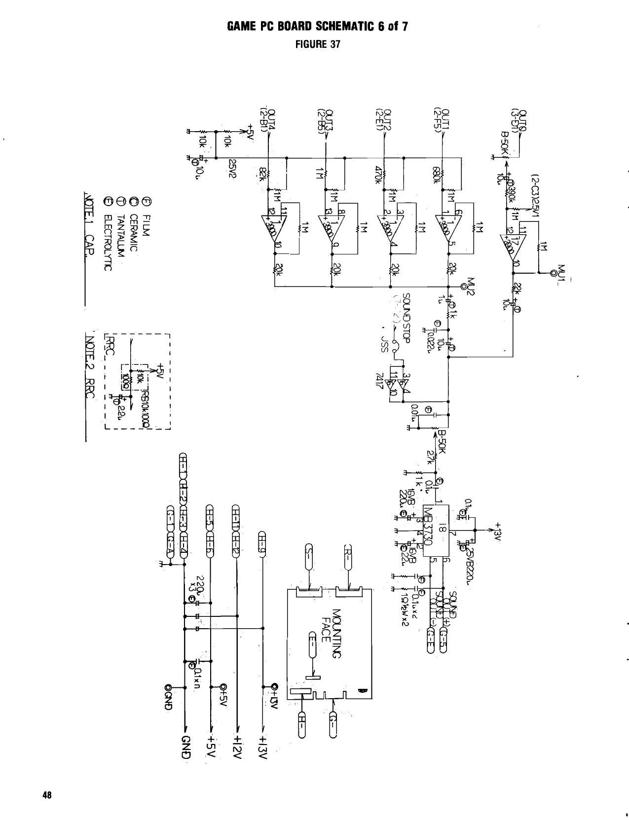
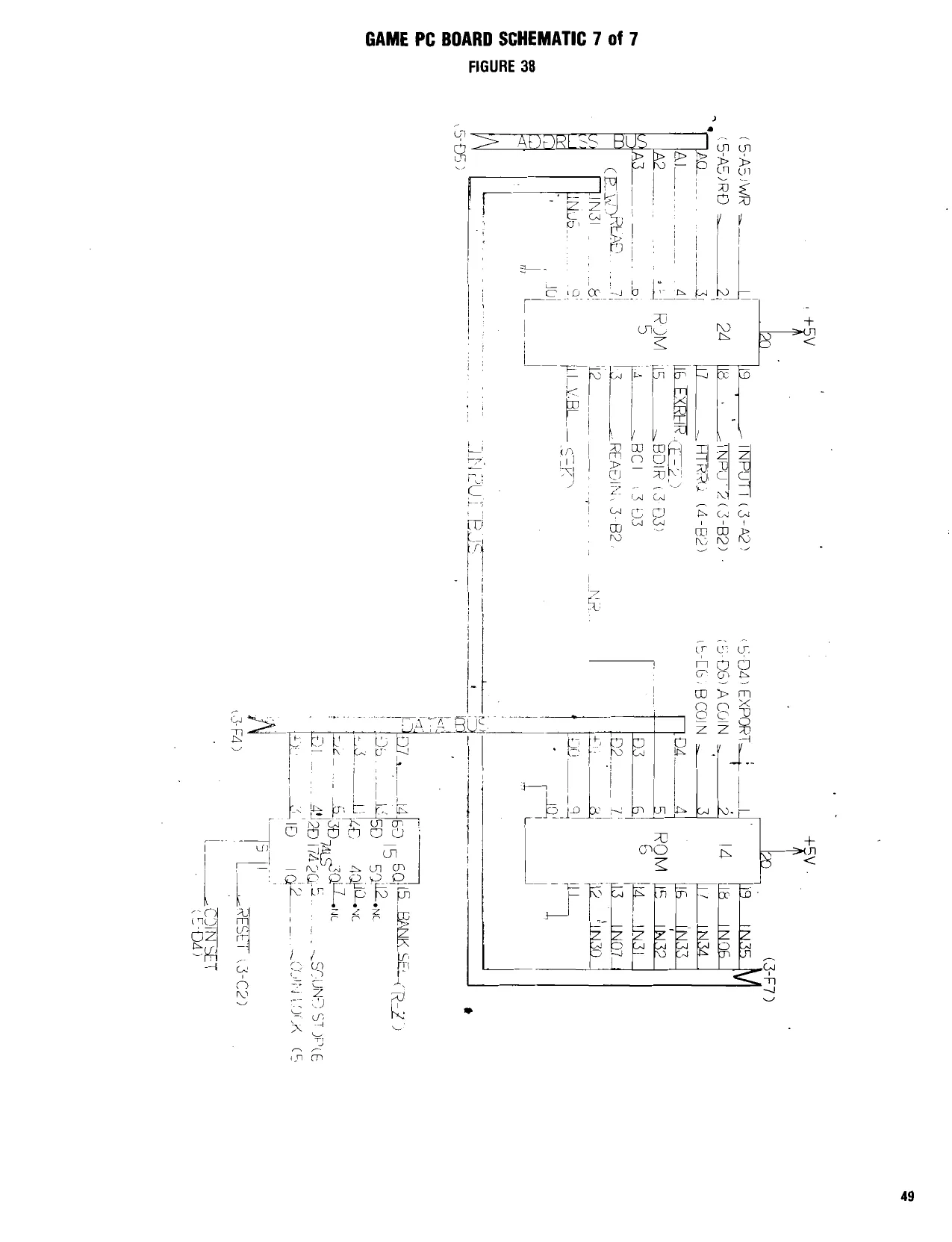
Figure 4 Video Monitor Removal . .. . 3 Figure 37 Game PC Board Schematic 6 of 7.............. 48 Figure 5 Cover Glass Removal ..........ceccsceeecseeead Figure 38 Game PC Board Schematic 7 of 7.............. 49
Figure 6 Printed Circuit Board Replacement ..............4 Figure’39 Wiring Diagram ...2ee-s+cvessoesseeeeereaes ”
Figure 7 Current Limit Adjustment........... nr)
Figure 8 Incandescent Panel................0.0000 eee 7 Figure 9 8-Way Joystick...... 0.0.0.2... cece eee eee 8 Figure 10 Control Panel 9
“JUNGLE KING” UPRIGHT
- GAME SET-UP A. INTRODUCTION
“JUNGLE KING"™ TAITO AMERICA CORPORATION’S ‘JUNGLE KING” game takes you deep into the jungle as ‘JUNGLE KING’ leaps from vine to vine, swims through a crocodile infested river, dodges falling boulders to save a beautiful girl who has been captured by barbarians. As the vines swing from left to right. time the swinging movements and push the Button to jump from vine to vine. Be careful of the monkeys that try to hamper your progress. Swing from the last vine and dive into the crocodile infested river. Push the Button to destroy the crocodiles with your knife and earn bonus points. Watch your air supply or your Jungle King will drown when the meter reaches “‘0"” Make it through the river safely - now run up the hill and jump over or duck under the failing boulders and find the beautiful Jungle Princess who is guarded by hostile barbarians. Use the Joystick Control and Button to jump over the barbarians and save the beautiful girl from her dangerous captors. An extra Jungle King will be awarded when scoring 10,000 (adjustable) points. The game ends when all Jungle King’s are lost or the game timer reaches “0”
B. GAME INSPECTION TAITO AMERICA’S CORPORATION'S “JUNGLE KING''™ upright game is ready to play when received. However, careful inspection is necessary to insure your game is in perfect condition. Please verify the following before turning the game on.
Examine external parts for chips, dents, or broken parts.
- Open the service door and examine the following:
- Plug-in connectors to make sure they are firmly seated.
- Speaker
- Player Controls
- Printed Circuit Boards making sure there is no damage to the components.
- Check for loose foreign objects, especially metal objects which may cause electrical problems.
- Fuses, making sure they are firmly in the holders.
- Coin Mechanisms
The Video Monitor is properly adjusted before shipping. !f there are any adjustments necessary refer to our Video Monitor Manual (72-00025- 001). If problems occur or technical assistance is required, contact our Customer Service Department HOT LINE Toll Free 800-323-0666 (except Illinois). Wlinois phone 312 981-1000 X215.
POWER REQUIREMENTS
TAITO AMERICA CORPORATION'S “JUNGLE KING’’™ upright game is shipped ready for operation at 120VAC, 60Hz with a power consumption of approximately 250 Watts.
For safe operation it is recommended the cabinet be grounded. This game is equipped with a three conductor power cable. The third conductor is the ground conductor and when the cable is plugged into an appropriate receptable, the game is grounded. The offset pin on the power cable's three-prong connector is the ground connection. LOCATION SPACE REQUIREMENTS
Depth - 35” (87.5cm) Width - 24” (61cm) Height - 68” (171cm) Weight - 300 Ibs. (Packaged Weight)
C. GAME INSTALLATION
The following precautions should be followed when installing the game
- Avoid rough handling of the game, the picture tube is fragile.
- Install the game on a level surface.
- Avoid installing the game where it may receive excessive sunlight or heat, to prevent the game from rising internal temperature.
- Do not install in a damp or dusty location.
- For a short time after connecting the power to the game, the picture may be temporarily distorted
D. DIP SWITCH AND VOLUME CONTROL SETTINGS
DIP SWITCHES TAITO AMERICA CORPORATION'S “JUNGLE KING’’™ upright game provides the following option switches. See Figure 1. These option switches can be found on the CPU Board (99KNN00004).
DIP SWITCH A
Position No Bonus Timer Remaining Fig x 1 Clearing| Timer Remaining Fig x 2 Bonus | Timer Remaining Fig x 3 Number of Jungle Kings
Test Mode Normal OFF
Test ON Screen 2P lorr |__| laversion 1-P ON Game 7 ‘OFF Style Upright ON
DIP SWITCH B
Setting Position 1 Coin - 1 Play 1 Coin - 2 Plays 1 Coin - 3 Plays 2 Coins - 1 Play 3 Coins - 1 Play 4 Coins - 1 Play
DIP SWITCH C
Position
(Not Added) |__ 10,000 Pts. on | oF | OFF Setting Bonus Points For Additional Jungle King 30,000 Pts. ON
1982" Not Display No Hit Of Player Coinage
OPTION SWITCHES B. FUSE REPLACEMENT
This game contains 8 fuses. Seven of these fuses can be found on the Power Supply Assembly, five (5) are on the PCB and two (2) are on the Power Supply Bracket. One (1) is located at the bracket where the AC line cord comes into the cabinet. See Figure (4) for location of these fuses.
FUSE REPLACEMENT < FIGURE 3 .
C. VIDEO MONITOR REMOVAL
If you need to remove the Video Monitor, follow the Instructions listed below.
It is recommended the game be left disconnected for at least one hour before removing the Video Monitor. This will probably discharge the Video Tube but EXTREME
rr) VOLUME CONTROL LOCATIONS
VA MAN 4 FIGURE 2 i u
VOLUME CONTROL SETTING The Volume increases by turning the potentiometer as indicated in Figure 2.
E. TEST MODE The following will be seen on the CRT screen while testing.
Normal Blue Background “RAM TEST White Letters NO RAM FAILURE’
No Letters 1C14, 56 on bottom Blue Background of CPU board
Letters On 1104 thru 109 Background will be Center of Video Board strange colors
2, MAINTENANCE All games require a certain amount of maintenance to keep them in good condition. A periodic check of mechanical controls would be beneficial to guarantee your game will be profitable.
A. CLEANING The exterior of the game, all metal parts and all plastic parts can be cleaned with an non-abrasive cleanser. Caution should be used when cleaning the plastic, a dry cloth can cause scratches and result in a foggy appearance. Disconnect power from the line voltage. Disconnect the Monitor cable connector. Remove the wire cable clamp. Take out the two side bolts, one on each side of the cabinet in order to lower the monitor. Remove the four mounting bolts and disconnect the green ground wire. Slide the Monitor out by pulling the Monitor toward you.
Use extreme caution and do not touch electrical parts of the Monitor Yoke area with your hands or with any metal object in your hands! High voltages may exist in any Monitor, even with power disconnected.
MONITOR REMOVAL
- VIDEO MONITOR ADJUSTMENTS TAITO AMERICA CORPORATION presently uses either a Wells-Gardner or an Electrohome 19” color monitor in the “JUNGLE KING’™ game. Refer to Monitor Manual (72-00025-001) tor your specific Video Monitor. Be sure to heed all the WARNINGS AND CAUTION INSTRUCTIONS provided before repairing or replacing your Video Monitor.
E. COVER GLASS REMOVAL To remove the Cover Glass follow the Instructions listed below:
- Remove the contro! Panel.
- Loosen three (3) screws on the Cover Glass, front bracket.
- Open Service Door and remove the (Rear\ Cover Glass Bracket.
- Slide glass up and out through the Service Door.
COVER GLASS REMOVAL
F. PRINTED CIRCUIT BOARD REPLACEMENT You may wish to remove the ‘JUNGLE KING'’™ Printed Circuit Boards for servicing. Refer to Figure 6. The “JUNGLE KING” Printed Circuit Boards are located on the inside of the Rear Service Door for easy access. To remove the boards the following steps should be followed:
- Open the rear service door, the power will automatically be removed by the Interlock Switch located on the inside of the door frame
- Disconnect the connector G, H, and T from the boards.
- Loosen and turn the Stop Bracket and pull the boards toward you out of the board guides.
PRINTED CIRCUIT BOARD REPLACEMENT G. POWER SUPPLY ADJUSTMENTS VOLTAGE Adjust voltages on +5V and +12V for +5.00V to +5.05V and +12.00V to +12.05V. CURRENT LIMIT Adjust control (Land 121) counterclockwise until voltage just changes, then turn control clockwise until voltage goes back to original value with pointer, mark position of arrow on Potentiometer then turn control until beginning of 1st notch is aligned with the pointer. On the controls with the Blue Disk turn approximately 30°.
CURRENT LIMIT ADJUSTMENT
- POWER SUPPLY The Power Supply produces all the necessary game voltage requirements.
A. AC INPUT The AC Input Voltage is applied to the main Power Supply via the AC Line Cords, Line Filter, Line Fuse, Power Switch and Interlock Switch. Different Line Cords are used for 120V and for 240V. The Line Fuse is located on the cine Cord Assembly near the Strain Relief. A Voltage Programming Block is located on the primary side ofthe Transformer to compensate for high/low voltage conditions The following line voltages may be inserting the appropriate Programming Plug.
Line Voltage Line Fuse
| 100 VAC + 10% | 50/60Hz | 3 AMP |
| 120 VAC + 10% | 50/60Hz | 3 AMP |
| 200 VAC + 10% | 50/60Hz | 1.5 AMP |
| 220 VAC + 10% | 50/60Hz | 1.5 AMP |
| 240 VAC + 10% | 50/60Hz | 1.5 AMP |
TABLE 3-1 LINE VOLTAGE
For continous protection against fire hazard, replace only with a fuse of the same type having the same electrical rating.
There are five secondary sources. Three go to the Regulator PCB providing +5VDC, +12VDC, —12VDC, and —5VDC. The other two are fused 6.3VAC used for the incandescent lighting and fused 120VAC used for the monitor, and in certain models for a fluorescent lamp and fan. These secondary fuses are located on the bracket adjacent to the Power Transformer. Secondary Fuse _| Circuit 120VAC 2.0AMP SLO-BLO 6.3VAC 2.5AMP
TABLE 3-2 SECONDARY FUSES B. —5VDC AND —12VDC REGULATORS The AC Input for the negative voltages comes into the Regulator PCB on J1-5 and J1-6 from the transformer. Fuse F3 protects against short circuits. The AC voltage is then full wave rectified by BR3 and filtered by C16. The raw DC is then applied to Reg 1, a three terminal —12V Regulator. The output of this Regualtor is the —12VDC output for the system and is also the input voltage for Reg 2, a —5V Regulator. The output of this Regulator is the —5VDC for the system. Capacitors C17, C18, C19 are to improve the transient response and stability of the minus voltage regulator. Diodes D8 and D9 provide protection against C18 and C19 being shorted through the Regulator. Resistors R34 and R35 provide current limiting for LED’S 3 and 4 which will light when there is voltage present at the regulation outputs. C. +5VDC REGULATOR The AC Input for the +5VDC Regulator circuit comes in on J1-4 and Ji-2, via F1 into BR1. BR1 full wave rectifies the AC Input. This raw DC is applied to the collectors of (2) series pass transistors, mounted on the Heat Sink Assembly. The regulation is done by U3, which is a voltage regulator whose output controis the gain of 5, which in turn controls the gain of the series pass transistors. The emitter of the series pass transistor return to the Regulators PCB and through R11 and R12, which serve to force current sharing between the series pass devices. The voltage at the output of R11 and R12 are the + SVDC for the system. R11 and R12 are voltage set and current foldback adjustments respectively. These are factory adjusted to 5V +.25V. at 7AMPS. Q8, D3 and R20 comprise a SCR-Type Crowbar Circuit which will trigger when the DC output voltages rise above 5.8V. Once the SCR fires , the Power Supply has to be turned off to reset the device. R19 is a current limiter for the voltage indicator LED 1. R16 is used to Set the output voltage of the Regulator. C8, D2, R13 and Q4 delay the start-up of the 5V Regulator to allow the —5VDC Regulator to stabilize first. D. +12V0C REGULATOR This circuit is essentially the same as the 5V Regulator described above. The AC current comes in on J1-3 and J1-4, via fuse F2 into BR2. The AC is rectified by BR2 and filtered by C9. The raw DC is fed to a single series pass transistor on the Heat Sink Assembly and also powers the +12V and +5V Regulator. R28 and R25 are voltage set and current foldback and factory adjusted to 12 Volts +.25V at 4 AMPS. D7, Q9, and R31 are SCR Crowbar Circuits which trigger at 13VDC output which causes supply to go inte Current foldback. There is an RC delay as in the SV circuit to delay the +12V rise time.
E, RESET CIRCUIT The reset circuit will output 2 2sec active low MRST pulse at J3-14 J4-14 when the power is first turned ON and whenever power fails for more than 35ms. The reset circuitry is comprised of a Dual Timer (556) and a fullwave type optical coupler across an AC secondary. The output of Ut is the input to one half of the 556 which is configured as a missing pulse detector. C1 and R3 determine the time before the output goes active. This is set for about 35ms. When two or more cycles are missing, the output of the first timer triggers the second timer which drives the MRST ow for about 2 seconds. The timer constant for the second timer is set by R4 and C6. Power on reset is generated by C4, and R39 and D12 on the trigger input of the second timer. Q3 inverts the signal out of the 556 so it is active low. R7 insures MRST is ow while the power is rising.
NOTES
INCANDESCENT PANEL
TAITO PART NO. DESCRIPTION 27-00006-001 | LAMP #47 26B00009-001 | BAYONET BASE SOCKET w]rm]a 61000112-001 | MARQUEE LIGHTING PLATE
8-WAY JOYSTICK
TAITO ITEM PART NO. DESCRIPTION 63B00031-001 | BALL & SHAFT 63A00033-001 | MASK 63C00027-001 | MOUNTING PLATE Blelm|a 62A00002-001 | SHOCK MOUNT PAD 63A00028-001 | SWITCH PLATE 62A00030-001 | ACTUATOR 61A00078-001 | "'L” BRACKET 63A00026-001 | SWITCH SPACER wclo/rlala 29800016-002| LEAF SWITCH r 10 63A00029-001 | SPACER 1 59B00020-017 | “E” RING
CONTROL PANEL
TAITO PART NO. DESCRIPTION 63B00031-001 BALL & SHAFT 63B00024-001 PUSH BUTTON, WHITE 42B00108-001 CLEAT, WOOD 63D00032-006 8-WAY CONTROL 61A00015-001 STRIKE HOOK 42D00017-001 CONTROL PANEL, WOOD 61D00251-001 CONTROL PANEL, METAL 63D00096-001 LEXAN DECAL 63-00025-001 SWITCH SUPPORT 54A07001-008 NUT, STAMPED 4-11 29B00016-001 LEAF SWITCH
DOOR ASSEMBLY
TEM TAITO PART NO. DESCRIPTION 61A00111-001 BRACKET, LOCK ROD 99KNNO0003 GAME P.C.B. 99KNNOOGO4 CPU P.C.B. sgwwoo002 VIDEO P.C.B 99KNNOOOOS ROM P.C.B. 08-00017-001 FILTER P.C.B. 07-00131-001 P.C, GUIDE ASSEMBLY 61A00014-001 “L" BRACKET Clo! |/ aaj alwjrmla 61-00142-001 LOCK ROD ASSEMBLY 08-00053-001 BOARD SET CONTAINS ITEMS 2,3,4,5
“Item not shown on drawing
DOOR ASSEMBLY
TAITO |. Tem | PARTNO. —_| DESCRIPTION 1 07-00027-001 | INNER PANEL WITH LEVERS SUB ASSEMBLY 2 54-03013-001 | NUT #8-32 ° 09-00017-001 | CUSTOM HARNESS ASSEMBLY (SHL) 08-00017-002 | CUSTOM HARNESS ASSEMBLY (DUAL) 3 | 61b00113-001 | SERVICE SWITCH BRACKET 4 29-00022-001 | SERVICE SWITCH 5 54-03011-001 | NUT #4-40 6 63-00014-001 | SWITCH COVER 7 51-02052-001 | SCREW #6-32 x 3/16 SS PH 8 23-00001-001 | C.R.E.M. COIL ASSEMBLY 9 51-02052-001 | SCREW #6-32 X 3/16 SS PH _ 10 59-00019-001 | RETAINER - 11 | 28-00029-001 | SILVER SWITCH WIRE FOR US. 25 12 29-00007-001 | SWITCH 13 61-00044-001 | COIN CHUTE 14 61-00045-001 | COIN RETURN BOX 15 | 61-00025-001 | SWITCH & C.R.E.M. COIL BRACKET 16 59-00018-001 | 25 ACCEPTOR - 7 51-02051-006 | SCREW 4-40 X 3/8 SS PH 18 27-00003-001 | MINATURE BAYONET BASE LAMP 19 27-00008-001 | #815 LAMP 20 61-0048-001 | COIN INLET CHUTE a1 61-00047-001 | RIGHT HALF OF COIN INLET CHUTE 2 54-00001-001 | “U" TYPE FASTENER 23 51-02051-006 | SCREW 4-40 X 1/2 SS PH 24 29-00006-001 | SLAM SWITCH ASSEMBLY 25 998325 COIN METER
“Iter not shown on drawing.
This page carries no recoverable text. It is a drawing or a photograph. See the original scan.
COIN DOOR
TAITO TEM PART NO. DESCRIPTION 1 61-00042-001 | COIN DOOR ONLY (2 COIN) c 2 07-00023-001 | COIN RETURN BUTTON ASSEMBLY FOR U.S. .25 COIN 3 63-00015-001 | COIN RETURN BUTTON [a 79-50004-001 | U.S. .25 PRICE DECAL 5 63-00016-001 | COIN RETURN BUTTON COVER FOR U.S. .25 COIN 6 07-00025-001 [LOCK ASSEMBLY [6A 07-00025-001 | LOK ASSEMBLY 7 51-01051-003 | SCREW #4 X 5/16 SL PH TYPE B 7A 51-01051-003 | SCREW #4 X 5/16 SL PH TYPE B 8 63-00011-001 | COIN BUTTON HOUSING 9 51-02051-002 | SCREW #4-40 X 1/4 SL PH 10 63-00012-001 | COIN RETURN BEZEL ni 63-00013-001 | COIN RETURN COVER 12 61-00040-001 | COIN RETURN FRAME 11 5/8 X 13 3/8 MOUNTS IN A 10 3/8 X 12 3/16 OPENING 13 54-01005-001 | HEX NUT 1/4 - 20 14 5103003-113 | CARRIAGE BOLT 15 07-00026-001 | LOCK ARM ASSEMBLY
COIN DOOR
CABINET ASSEMBLY FRONT VIEW
TAITO
| ITEM | PART NQ. | DESCRIPTION |
07M00055-002 |INCANDESCENT PANEl. ['63800006-003 |"U~ CHANNEL BRACKET 47-00012-012 |MARQUEE 61000115-001 {| MARQUEE RETAINING BRACKET
07-00217-001 |CONTROL PANEL ASSEMBLY 07-00114-001 | COIN DOOR 5 61D00012-003 [LOWER COVERGLASS BRACKET
61B00113-001 | SWITCH BRACKET
| [3 | ['07-00118-001 | SERVICE SWITCH ASSEMBLY | 7 | _ | - | |
| 10 | 29-00022.001 |SLIDE, CENTER RETURN SWITCH | 7 | : | _ | |
| " | 29800015-001 |INTERLOCK SwITCH | _ | — | _ | |
| 12 | 61800114-001 |INTERLOCK SWITCH | ; | _ | ||
| 13 | 59-00008-001 | |LATCHING CLAMP | _ | _ | _ |
| (14 | 63800002-004 | |"T MOLDING | —_ | _ | |
| 15 | 29A00023-001 | POWER ON OFF SWITCH | _ | |||
| : | 09-00227-001 | NAN HARHESS CABLE | - |
: 09-00043-001 | SPEAKER CABLE _ : 59-00046-001 [SWITCH BARRIER
“Item not shown on drawing.
CABINET ASSEMBLY FRONT VIEW
CABINET ASSEMBLY REAR VIEW
[Taito INEM —|PARTNO. _ [DESCRIPTION 1 07-00083-001_|SPEAKER 2 61800038-001 [SPEAKER GRILL 3 41-00015-007 [FINISHED CABINET 4 63C00005-004 |""L" MOLDING 5 07M00042-001 [A/C LINE CORD ASSEMBLY 5A ___| 22-00001-001 [LINE FILTER 8 83C00005-002 |"L" MOLDING 7 61800030-002 [INTERLOCK BRACKET 8 29B00015-001 |INTERLOCK SWITCH 9 07M00039-001 [POWER SUPPLY *9A 18-00003-001 | TRANSFORMER *9B 08-00007-001 [BOARD “90 07-00041-001 [HEAT SINK ASSEMBLY 10 61600054-001 [CASH BOX LID 1 61000060-001 [CASH BOX 12 07M00054-001 CASH TRAY ASSEMBLY 13 63R00010-001 [CASH TRAY (ONLY) 14 63-00019-001 [CASH TRAY SEPARATOR 15 61B00039-001 [CASH TRAY HANDLE 16 42C00013-001 [MONITC SUPPORT CLEAT 17 61D00208-001 [CRT SUPPORT FRAME 18 31-00013-001 |19” COLOR MONITOR [19 26B00008-001 | SOCKET LAMP 20 27-00006-001 | #47 BULB 21 47-00016-004 | COVERGLASS 22 63D00053-001 | MONITOR SHROUD 23 61C00006-001 | UPPER COVERGLASS BRACKET 24 61-00142-001 | LOCK ROD ASSEMBLY
25 04-00037-002 [LOCK ASSEMBLY 26 44C00001-001 | WHEELS
- 59-00045-001 | SWITCH BARRIER
“Item not shown on drawing
CABINET ASSEMBLY REAR VIEW
FILTER BOARD
TANTO ITEM | PARTNO. —_| DESCRIPTION QUANITY
| 1 | 12-10003-471 | Cap, 470pf + 10% Axial Lead | 74 | |
| 2 | 17-00001-001 | Ferrite Bead Assembly | 42 | |
| 3 | 25-00002-014 | Connector 14P | q | |
| 4 | 25-00002-005 | Connector SP | 2 | |
| 5 | 14-23904-001 | Transistor NPN 2N3904 | 1 | |
| 6 | 11-00001-102 | Resistor 1K ohm %4W. | 1 | |
| 7 | 11-00001-332 | Resistor 3.3F ohm %W | 2 | |
| 8 | 63B00068-001 | Stand Off | 8 | |
| OT] | 2 | Lf | LS conn, 5 pw |
é 8 Si rPatjs
| [| | 4 | P| o> |
ot ! BFe 48 y :
| cD | os | O38 |
| ella | lis | 4 |
- FERRITE BEADS
| | | i | 3 |
er ii
| eS | i> = | 2) | S |
lola 4b
| = (ye | Ee | ® | TRANSISTOR |
{ ep-——RESISTOR
| = | jj} | or | LoS | PL—-nesiston |
TUE so aoe
| SS | | | | its | ||
| a | i | ii | | | cD |
| \ | <| | |« | = | |
| =| | |< | cS |
| -S-cown 4p i CJ
- | APACITOR fou RESISTOR
- ry] se
| = | ES | o |
g eS gg s| | <2 eg S32 8 = i UJ
POWER SUPPLY
TAITO TAITO SYM | PART NO. DESCRIPTION SYM | PART NO. DESCRIPTION
| )Rt | 11-00001-102 Resistor 1.0K 5% YaW 5% | C5 | | 12-10001-102 | Capacitor, .0O1uf |
R2 | 11-00001-512 | Resistor 5.1K YW 5% C6 | 12-30001-106 | Capacitor, Tantalum 10uf
| R3__| | 11-00001-183 | Resistor 18K %W 5% | C7 | 12-20003-509 | Capacitor, Electrolytic 50,000uf |
R4 | 11-00001-224 | Resistor 220K vsW 5% C8 =| 12-30001-105 | Capacitor, Tantalum 1.uf 35V R5 | 11-00001-472 | Resistor 4.7K YW 5% C9 | 12-20003-209 | Capacitor, Electrolytic 20,000uf RG | 11-00001-222 | Resistor 2.2K %4W 5% C10 | 12-10001-332 | Capacitor, Ceramic .0033uf
| R7_| | 11-10001-101 | Resistor 100 “MW 5% | C11_| | 12-30001-476 | Capacitor, Tantalum 47uf |
R8 | 11-00001-102 | Resistor 10K %W 5% C12 | 12-30001-105 | Capacitor, Tantalum 1.uf 35V RQ | 11-00001-472 | Resistor 4.7K YW 5% C13 | 12-10004-103 | Capacitor, Ceramic .O1uf R10 | 11-10001-101 | Resistor 100 YeW 5% C14 | 12-10001-102 | Capacitor, .001uf R11 | 11-30001-015 | Resistor .15 4W 5% [cis | 12-30001-476 Capacitor, Tantalum 47uf R12 | 11-30001-015 | Resistor .15 4W 5% C16 | 12-20002-108 | Capacitor, Electrolytic 1,000uf
| R13 | 11-00001-472 | Resistor 4.7K YW 5% | C17_| | 12-30001-225 | Capacitor, Tantalum 2.2uf 25V |
R14 | 11-00001-222 | Resistor 2.2K %W 5% C18 | 12-30001-225 | Capacitor, Tantalum 2.2uf 25V R15 | 11-00001-222 | Resistor 2.2K Y¥4W 5% C19 | 12-30001-105 | Capacitor, Tantalum 1.uf 35V R16 | 11-60001-252 | Pot 2.5K YaW 20% F1 | 24-00003-010 | 10A Fuse R17 | 11-00001-222 | Resistor 2.2K YW 5% F2 | 24-00003-010 | 10A Fuse
| R18 | 11-60001-102 | Pot 1.0K %W 20% | F3__ | | 24-00003-003 | Fuse, 2A |
R19 | 11-00001-511 | Resistor 510 4%4W 5% F4 | 24-00003-004 | Fuse, 4A R20 | 11-10001-470 | Resistor 47 YW 5% F5 | 24-00003-004 | Fuse, 4A R21 | 11-00001-162 | Resistor 1.6K YW 5% BR1 | 13-00100-025 | Diode Bridge 254, 100V R22 | 11-00001-103 | Resistor 10K %W 5% BR2 | 13-00100-012 | Diode Bridge 12A, 100V R23 | 11-00001-472 | Resistor 4.7K %W 34 BR3 | 13-00100-002 | Diode Bridge 2A, 100V R24 | 11-00001-222 | Resistor 2.2K ¥sW 5% 7 D1 | 13-14002-001 | Diode IN4002 R25 | 11-60001-102 | Pot 1.0K %4W 5% D2 | 13-14002-001 | Diode IN4002 R26 | 11-00001-472 | Resistor 407K YaW 5% D3 | 13-10752-001 | Diode, Zener IN752 R27 | 11-00001-222 | Resistor 2.2K YW 5% D4 | 13-14002-001 | Diode IN4002 R28 | 11-60001-252 | Pot 2.5K YW 20% D5 | 13-14002-001 | Diode IN4002 R29 | 11-00001-472 | Resistor 4.7K %W 5% D6 | 13-14002-001 | Diode IN4002 R30 | 11-00001-122 | Resistor 1.2K %4W 5% 07 __| 13-10964-001 | Diode, Zener IN964 R31 | 11-10001-470 | Resistor 47 %4W 5% D8 | 13-14002-001 | Diode IN4002 R32 | 11-30001-015 | Resistor .15 4W 5% D9 | 13-14002-001 | Diode IN4002
| R33_| | 11-00001-222 | Resistor 2.2K Y4W 5% | 010 | 13-14002-001 | Diode IN4002 |
R34 | 11-00001-122 | Resistor 1.2K %W 5% 011 | 13-14002-001 | Diode IN4002 R35 | 11-00001-511 | Resistor 510 %W 5% 012 | 13-14002-001 | Diode IN4002 R36 | 11-00001-222 | Resistor 2.2K YaW 5% LED1| 13-00001-001 | LED (Red) R37 | 11-00001-104 | Resistor 100K LED2| 13-00001-001 | LED (Red) R38 | 11-00001-103 | Resistor 10K %4W 5% LED3} 13-00001-001 | LED (Red) J R39_ | 11-00001-224 | Resistor 220L YW 5% LEO4| 13-00001-001 | LED (Red)
| C1 | 12-30001-225 | Capacitor, Tantalum 2.2uf 25V | U1__| | 15-62500-001 | Opto Coupler H11AA2 |
C2 | 12-10004-103 | Capacitor, Ceramic .Otut U2 | 15-50556-001 | Timer (Dual) 556 C3 | 12-10004-103 | Capacitor, Ceramic .Otuf U3 | 15-50723-001 | Voltage Regulator 723 C4 | 12-30001-105 | Capacitor, Tantalum 1.uf 35V U4 | 15-50723-001 | Voltage Regulator 723
POWER SUPPLY
TAITO [ SYM | PART NO. | DESCRIPTION REG1| 15-57912-001 | Voltage Regulator 7912 REG2| 15-57905-001 Voltage Regulator 79L05 Qt | 14-22905-001 | Transistor 2N2905 02 | 44-22905-001 | Transistor 2N2905 Q3 | 14-22905-001 | Transistor 2N2905 Q4 | 14-22905-001 | Transistor 2N2905 Q5 | 14-23055-001 | Transistor 2N3055 Q6 | 14-22905-001 | Transistor 2N2905 Q7 | 14-20030-001 | Transistor TIP-30A | Q8 | 14-26401-001 | SCR 2N6401 Q9 | 14-26401-001 | SCR 2N6401 _| ti 25-00022-008 | Connector, 1-380999-0 6Pin 32 | 25-00022-008 | Connector, 350212-1 8Pin 3 25-00002-014 | Connector, 09-60-1141 14Pin J4 | 25-00002-014 | Connector, 09-60-1140 14Pin 24-10001-001 | Fuse Clips 30-00220-002 | Heat Sink Dual To-220 [30-00003-007 | Heat Sink Single To-3
vs
vs » a POWER SUPPLY COMPONENT LAYOUT
+
i371) 23:3} a sand : | ue ws wi ZaWW 100-20000-80
oe, Te s+ nWOO
Azit O© gBRE
en
()aBREC) BE Ear Abbe g OO Ri B OO
oN Ww
a esvs
vs!
This page reads as a drawing: its text was drawn rather than typeset, and comes out in fragments. See the original scan.
ROM BOARD COMPONENT LAYOUT
This page reads as a drawing: its text was drawn rather than typeset, and comes out in fragments. See the original scan.
CPU BOARD COMPONENT LAYOUT
240) t [ | a. | Fe ar eee p at /. a a gang @ ao, Lc op O Nai) ER 3 P C ASD
@ On @ 6 s\enge ae wae oa _
“Pee CZ _ oes BER, ee haa rota cas) me renee . Race: —ea, as
“et § i
00! 02.10 OINVHRO ‘d¥9| SIElPLYV-66 ee) 98STrZ 91-S7 290881 VV-66 StOl] be ZOOOONMM Y3NDILS GUVOS 9 d|20Z0Z0MM-66 is €8S1rZ 91-7 6SOLELVY-66 vol] €@ SLNIW313 8 WHO 4b 49018 YOLSISIY| 9E0SS1VV-66 au plSTrd OI-S1 LSOeeLVV-66 %S Mp/k WHO | NOBYVO ‘S3u| S9ZLS1VV-66 ed eeSipd O-S1 L208 LWV-66 e101 zz ziai| 12 %G Mb/t WHO OZp NOGYWO ‘S3u| ZSZ1SIVV-66 tu oesirZ JI-S7 9Z0EELVY-66 LLoW} Oz AL-SEISS WNTWINVL ‘dVO] 9ePLyLWy-66 2) 2@S1bd OI-S1 veoce.wv66 | d08}-602-L0 DINVYSO 'd¥O| Peel PLVW-66 £9 O@STrZ OI-S1 6LOgelLVV-66
Olol; 6b 601 [- POI-HI-AGL W1Id ‘d¥O| prep lvy-66 OLSTrZ OI-S1 bLOeeLVV-66
al 891 ri OZZAA9! ILAIOYLOITA ‘dvO}] €2OLPLVW-66 4o 80STrZ II-S1 600EELVV-66 Zot] 9k Gasn LON vOSTrZ 9I-S7 SOOEELVY-66 901} St ZIMM (282S¢2) WOH er WOU 20S Ir OS1 £008ELVY-66 Sol] bb é9ESThL II-S1| 660ZELVY-66 8291 O0STPrZ O1-S7 LOO LWY-66 val] eb pleSTrZ MIST] 6OCEELWY-66 2291 eepes WH Og LZeivv-66 eo] 2b L£9€STrZ IST] COCEELVY-66 9291 d9LOZWWL WY OILVLS BL IZELVV-66 el} otk €L2S 1rd II-S1| OLLEELW¥-66 Szol e-7b be NVY JLLWLS e9bzelvv-66 Lol] ob €S2SbZ II-S1| E9beeivv-66 veo! LuOddNs dYvO LINDYID SNINIOT 68S690VV-66 EM) SZISTbZ DIST] 82IEELVV-66 £291 diHO LNIOd LS3L LSS9SOVV-66 dl PLiSThL DI-S1| LZLEELWV-66 2291 d2z 1390S 91 666SS0VV-66 vSi 99LSThZ DIST] IZLeelvv-66 1291 dre Lay008 91 2£82SS0VV-66 esl POLSTPZ OI-ST| GLLEELWY-66 0291 dg} 1390S 91 98ZSSOVV-66 €9lSTrZ DIST] SLLECLVV-66 6LO1 d8t L3¥00S Ot eG LSSOWV-66 AS1SThZ II-S1| ZLLEELW¥-66 8Lol d0S ASSY SSANHVH 9Y4 29200SV¥-66 €SLSTbZ IST] BOleeivy-66 210! gasn LON alol+}w]oln|ola 6ELSTrZ DI-S1| Z60ee1VV-66 gtr GYVvO8 Id OAGIA 200020MM-66 t NOLLdIY9S3C “ON Lud OLIVL WAS WAL NOMd1¥9S30 “ON LuVd OLIVE WAS | WALI 02 3uNDId quvod O3CIA
8, | F Sanne “BaRGaRa, | aaasag s3.Bballae 6 Sanpall|.ashaaaa canst FEEL
TAITO TaITO
| tem| sym | PARTNO. | OESCRIPTION | rem|sYM | [PART NO. | | DESCRIPTION | ||||
| 1 | 99-KNNOOO03 [ GAME PCB | 47__[ic24__ | | 99-AAT36105 | [CMOS MB14584 | |||
| 2 | [185 | | 99-AA055103 | IC SOCKET 18P | 48 | [i265 | _|99-AATS2003 [TTL-I¢ 7404 | ||
| 3 | [Ds | | 99-Aa0s2s66 | DIP SWITCH | 49_ | [1026 | [99-AAT32099 [TTL 1C 74367 | ||
| 4 | |12P _ [99-Aa056115 | SL56 POST HEADER 12P | 50 | [ic | _[99-AAT32019 [TTL IC 7404 | |||
| 5 | _|30P | 99-AA055160 | CONNECTOR PLUG HKP-30M | 51 | [1028 | __[99-AATs2011 | [TTL IC 7474 | ||
| 6 | [181 | | 99-AA055169 | 1C SOCKET 26P | 52 | [1029 | 99-AATS2161 | [TTL IC 74273 | ||
| 7_[50P | 99-AA055910 | ANGLE PIN HEADER PS-S0PA | 53 | NOT USED | |||||
| 8 | |1s2__| | 89-AA055787 | 1C SOCKET 24P | 54 | [C1 | [9%-AAT41019 | [CAP, ELECTROLYTIC 16VB220 MF | |
| 9 | [183 | 99-aA055817 | 1C SOCKET 40P | 55 | [C2 | |99-AAT41023 | CAP, ELECTROLYTIC 16vB220 | ||
| 10 | _[is4 | | 99-AA05s815 | [IC SOCKET 20P | 96 | [C3 | [99-AAT41298 | [CAP, FILM TDY-1M-103 |
| 11_[TP | | 99-Aa0s6551 | TEST POINT | 57__[04 | | 99-AAT¢1740_ | CAP, FILM TOY-1H-223 | |||
| 12 | [CB | | 99-AA060557 | LOCKING CIRCUIT BOARD | 58 | [C5 | [99-AAT41244 |CAP, FILM TOY-1H-104 | ||
| SUPPORT | 59 | [C6 | __[99-AAT41310_[CAP, CERAMIC 47PF 50V | ||||
| 13_[TR1__ | | 99-AAT11040 | TRANSISTOR 250423 | @0 | ler | |oa-aaTat242 TAP. FILM | |||
| Li | PAN HD SCREW MSX6 | 61 | [C8 | |99-AAT41322_|CAP, CERAMIC 150PF 50V | |||
| 15 | es | 62 | [co | | 99-AAT41374 | |CAP, CERAMIC 180PF 50V | ||
| E | TRG __ | 99-AAT110701 | THANSISTOR 250635 | 63 | [C10 | [99-AAT41302 | [CAP CERAMIC 22pf SOV | ||
| ud | PAN HD:SGREW MAX6 | 64 | [C11 _ [99-AAT41334 | [CAP, CERAMIC 470PF 50V | |||
| 18 | ore | 65 | [C12 | |99-AAT41430_ | |CAP, TANTALUM SSG25-10F | ||
| 19_[OP1__|99-AAT31011_| | OP AMPLIFIER 1M3000 | 66 | [C13 | _[99-AAT41431_|CAP, TANTALUM SSG35-OR1F | |||
| 20_|0P2__| | 99-AATS1050_| | OP AMPLIFIER MR3230 | 67 | [C14 | _|99-AAT41436_|CAP, TANTALUM SSG35-1F | ||
| a | PAN HD SCREW MaXé | 68 | [C15 | _[99-AAT41432_[CAP, TANTALUM SSG35 7R2F | |||
| 2 | NUT M3 | 69 | [R1 | __[99-AATS1741 | [RES, CARBON 100 OHM 1/2W 5% | ||
| 23 | {IGA | | @9-AATS2089 | TTL: IC 7416 | 70 | [R2___ | |99-AATS1749 | [RES, CARBON 220 OHM 1/4W 5% | |
| 24 | [1G2_| | 99-AATS2040 | TTLIG 7417 | 71 | _[R3___|99-AATS1751_|RES, CARBON 270 OHM 1/4W 5% | |||
| 25_|1G3_| | 99-AATS2163_| STATIC RAM 2114.2 | 72__[R4 | __[99-AATS1753_[RES, CARBON 330 OHM 1/4W 5% | ||||
| 26 | _|1G4_| | 99-AATS2165 | SOUND IC AY38910 | 73 | [RS | __|99-AATS1759 | |RES, CARBON 560 OHM 1/4W 5% | |
| 27_|1C5_| | 99-AATS2179 | TTL - RAM 95410 | 74__[R6 | __|99-AATS1757_[RES, CARBON 470 OHM 1/4W 5% | ||||
| 28 | |1C6__| | 99-AAT33001 | LS-IC 74L800 | 75 | _[R7 _ [99-AATS1765_[RES, CARBON 1K | |||
| 29 | [1c7__{ | 99-AATS3003 | LS-IC 74LS02 | 76 | _[R8 | _|99-AATS1779 | |RES, CARBON 3.9K 1/4W 5% | |
| 30_|1€8_| | 99-AAT33005_| | LS-1C 74.804 | 77 | [RO | |99-AATS1781 | [RES, CARBON 4.7K OHM |
31_fico | 99-AAT33008 | LS-Ic 741808 AW 5%
| 32 | [ict _| 99-AAT33027 | TI (ONLY) 74.837 | 78 | [R10 | [99-AATS1789 | [RES, CARBON 10K 1/4W 5% | ||
| 33_[ictt | 99-AaT33051 | [LS-IC 741874 | 79_[Ri1 _ [99-AATS1796_[RES, CARBON 20K OHM 1/4W 5% | |||||
| 34 | fice | 99-aar3a020 | [LS-IC 74.896 | 80 | [R12 | [99-AATS1797 | [RES, CARBON 22K OHM 1/4W 5% | |
| 35 | _[ict3 | 99-aaT3a096 | LS-IC 7418138 | 81 | [R13 | __[99-AATS1603 | [RES, CARBON 39K OHM 1/4W 5% | ||
| 36 | NOT USED | 82 | [R14 __ |99-AATS1775 | [RES, CARBON 82K OHM 1/4W 5% | |||
| 37 | ficts _ | 99-AaT33108 | [LS-IC 7418153 | a3 | [R15 | _[99-AATO1811 | [RES, CARBON 82K OHM 1/4W 5% | |
| 38 | [ic16 | _[99-aaT33t10 | [1S-IC 7aLS185 | a4 | [R16 | _[99-AATO1812 | [RES, CARBON 100K 1/4 W 5% |
| 39 | [ict7 | 99-AATS3163 | LS-IC 7418253 | a5 | _[Ri7 _ [99-AATS1823 | [RES, CARBON 270K 1/4W 5% | |||
| 40 | [icts | 99-aArs9164 | [LS-IC 7418257 | a6 | [R18 | _[99-AATS1825 | [RES, CARBON 330K 1/4W 5% | |
| ai_[ici9 | _[99-AaTsat66 | s-1c 7418259 | 87 | [R19 | _[99-AATS1627_[RES, CARBON 390K 1/4W 5% | |||
| 42_[c20__ | | 99-aATast27 Tisac TALS174 | 88 | [R20 | |99-AATS1629 | [RES, CARBON 470K 1/4W 5% | | ||
| 43 | [ict | [99-aar33203 | Ls-IC 7418367 | a9 | [R21 | _[99-AATS1833_[RES, CARBON 680K 1/4W 5% | ||
| 44 | [ic | [99-aata3z09 | LS-IC 7418374 | @0 | [R22 | _|99-AATS1037 | [RES, CARBON 1M OHM 1/4W 5% | |
| 45 | [ices _ | 99-AaT33220 | LS-IC 7418393 | 91 | [R23 | |99-AATS1733._[RES, CARBON 47 OHM 1/4W 5% | |||
| 46_[cPU | 99-AAT34008 | CPU Z-80A | 92 [R24 | [99-AATS1771_[RES, CARBON 47 OHM 1/2W 5% |
GAME BOARD
TAITO
| ITEM | SYM | PART NO. | DESCRIPTION | |
| 93 | | R25 | 99-AAT51845 | |RES, CARBON 22M OHM 1/4W 5% |
94 | R26 99-AAT51847 _|RES, CARBON 22M OHM 1/2W 5%
| 95 | [R27 | 99-AAT51772_|RES, CARBON 2K OHM 1/4W 5% |
| 96 | R28 | 99-AAT51068 | |RES, CARBON 15 OHM 1/4W 5% |
| g7 | [R29 | 99-AATS1969_|RES, CARBON 30K OHM 1/4W 5% |
| 98 | R30 | 99-AATS1971 | _|RES, CARBON 1M OHM 1/4W 5% |
99 | R31 99-AAT51982 |RES, CARBON 1 OHM 1/4W 5%
| 100 | |VR | 99-AAT53041_)RES, VARIABLE RESISTOR B-SOK |
| 101 | RB1 | 99-AAT55036 | |RESISTOR BLOCK 1K OHM |
8 ELEMENTS
| 102 | |RB2 | 99-AATS55061 | RESISTOR BLOCK 10K+100 |
OHM 108 109 | R32 99-AAT55033 / WINDING RESISTOR 6 OHM 2W 10% 104 NOT USED
| 105 | 4202 | 99-AAT13042_|FENNER DIODE RD2 7FBF |
| 106 | |203 | 99-AAT13028_|FENNER DIODE RDQA-M |
107 | ST 99-£€070004 | HARNESS STICKER
| 108 | |ST2 | '99-KNO70203 | PCB STICKER KNOO003 |
| 110 | |ROM1 | |99-KN090437 | PROM (2732) KN37 |
111_|ROM 2 |99-KN090438_| PROM (2732) KN38 112 |ROM3 |99-KNO90439 | PROM (2732) KN39 113 NOT USED 114 NOT USED
| 115 | |X-TAL | {99-AA069593_| | X-TAL 6MHz |
116 99-AA062644_ | JUMPER WIRE |
GAME BOARD COMPONENT LAYOUT
@ (a) @ @Qq @ @® ie CS EEG ne) HEIR Sa ems mic or ee, = eer 8 Ss se) ars Ba ica ao a D
- b y . ©)
{| OD0000000x00 II
POWER SUPPLY SCHEMATIC 1 of 1
TSS Ta wim © wis! @ [Sy F1ve olop vir 89 ly 80 is,
AGt ROM PC BOARD SCHEMATIC 1 of 1
CPU PC BOARD SCHEMATIC 1 of 3
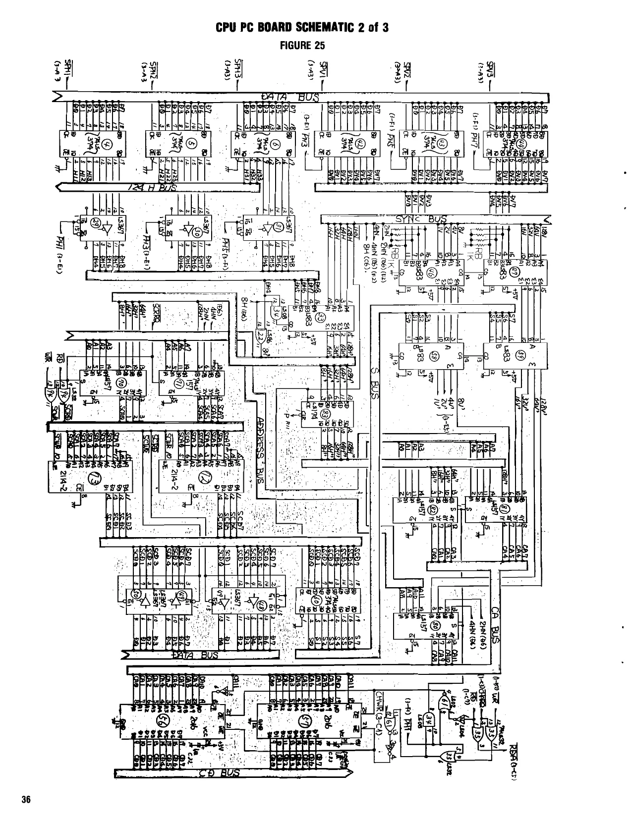
This page is a drawing, shown as the original scan.
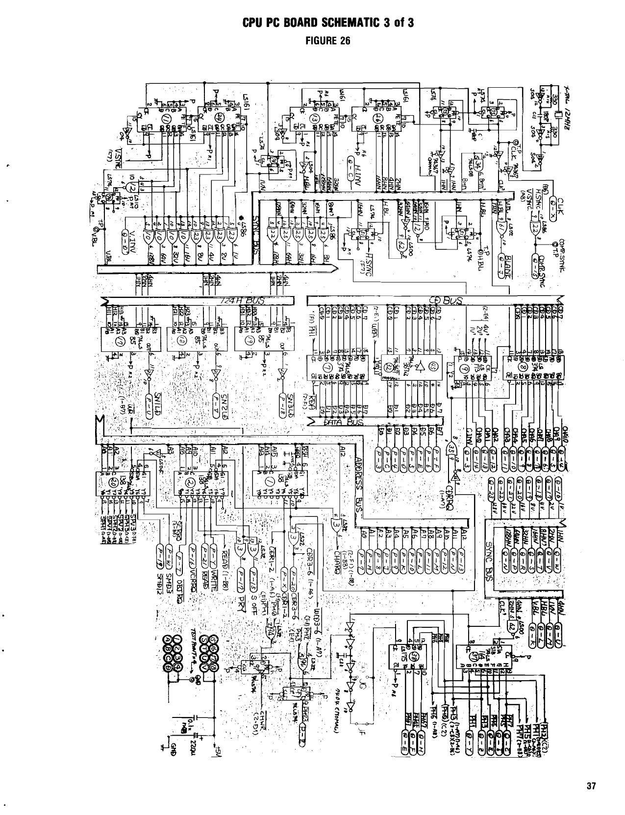
This page is a drawing, shown as the original scan.
VIDEO PC BOARD SCHEMATIC 1 of 5
ary an
ONG. cong al BeoSeEsa) A 1G Aw IN <<<x
“7+3-A7)CLK1—_, 1 81 64 SHIGE 558 -C) re a A
|, —SN2OFF arf (4-CA)
SNSOF ff aC) (246)
On, 7?
VIDEO PC BOARD SCHEMATIC 2 of 5
~ rag <o MA
(4-Day
(CL KHG-A) a a la a REED DTTOODD) ap &E ° Qtr
fel a ts} lo%p blelelabs TOTMoEOOD]
e i ne
SoOsOoG | 8 pa are! (2-—-SNIOF OM) ,
VIDEO PC BOARD SCHEMATIC 3 of 5
LCLK (A7) ~ OMA: GB) ris ik +
aD (9; PANIT Pi Z3-) | evastw. Al e8 ay “t F acler ike g T ce] raxq vi 22 53 SOY) v a een ”
- 2YCEO" VIDEO PC BOARD SCHEMATIC 4 of 5
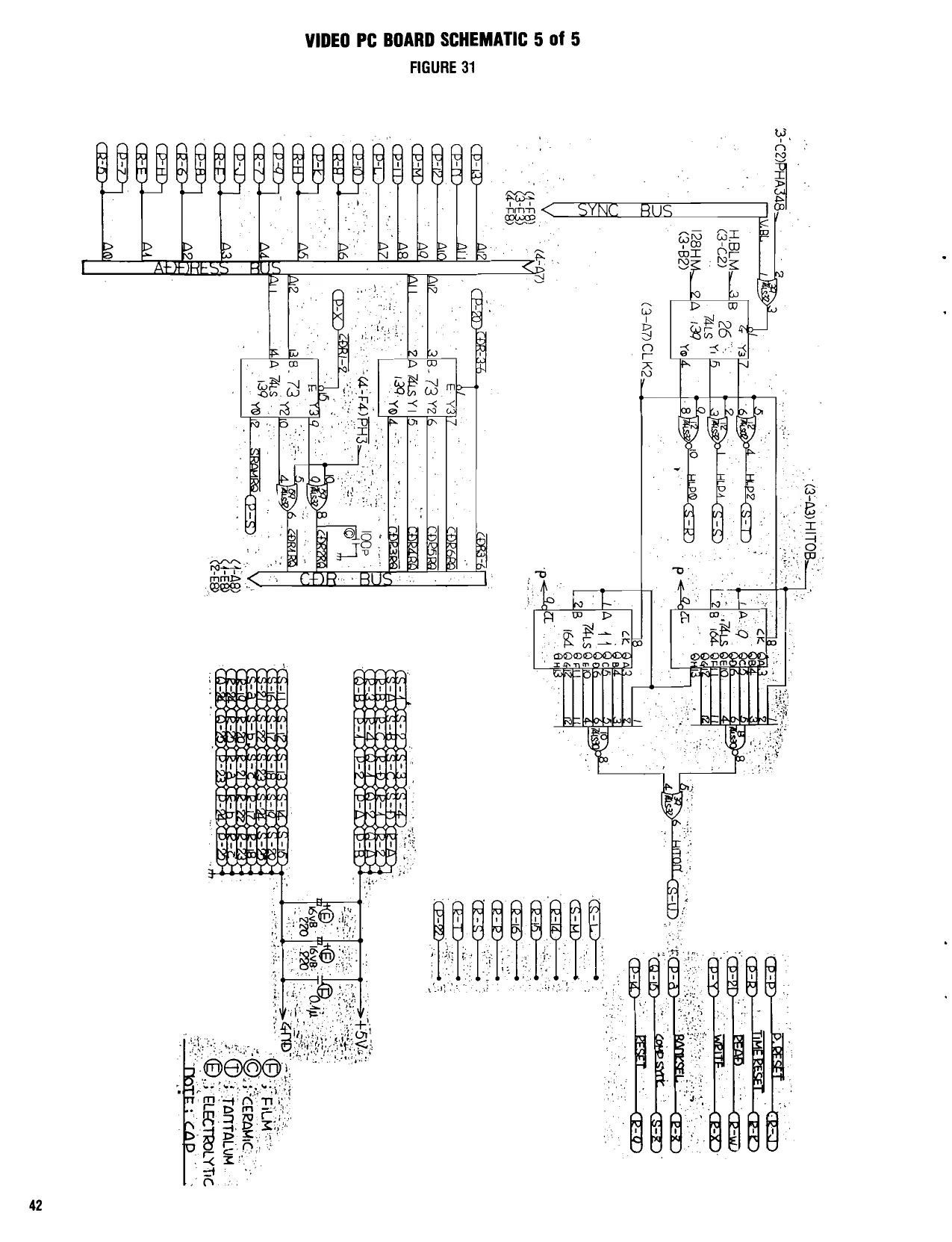
This page is a drawing, shown as the original scan.
GAME PC BOARD SCHEMATIC 1 of 7
GAME PC BOARD SCHEMATIC 2 of 7
GAME PC BOARD SCHEMATIC 3 of 7
(2-B5) ee eee 7
AWAY OR 2WAY
(5-D8)
(9-S)
- (93-1) Tro? 7 q DSL 96512 a1 es le uw OL GAME PC BOARD SCHEMATIC 4 of 7
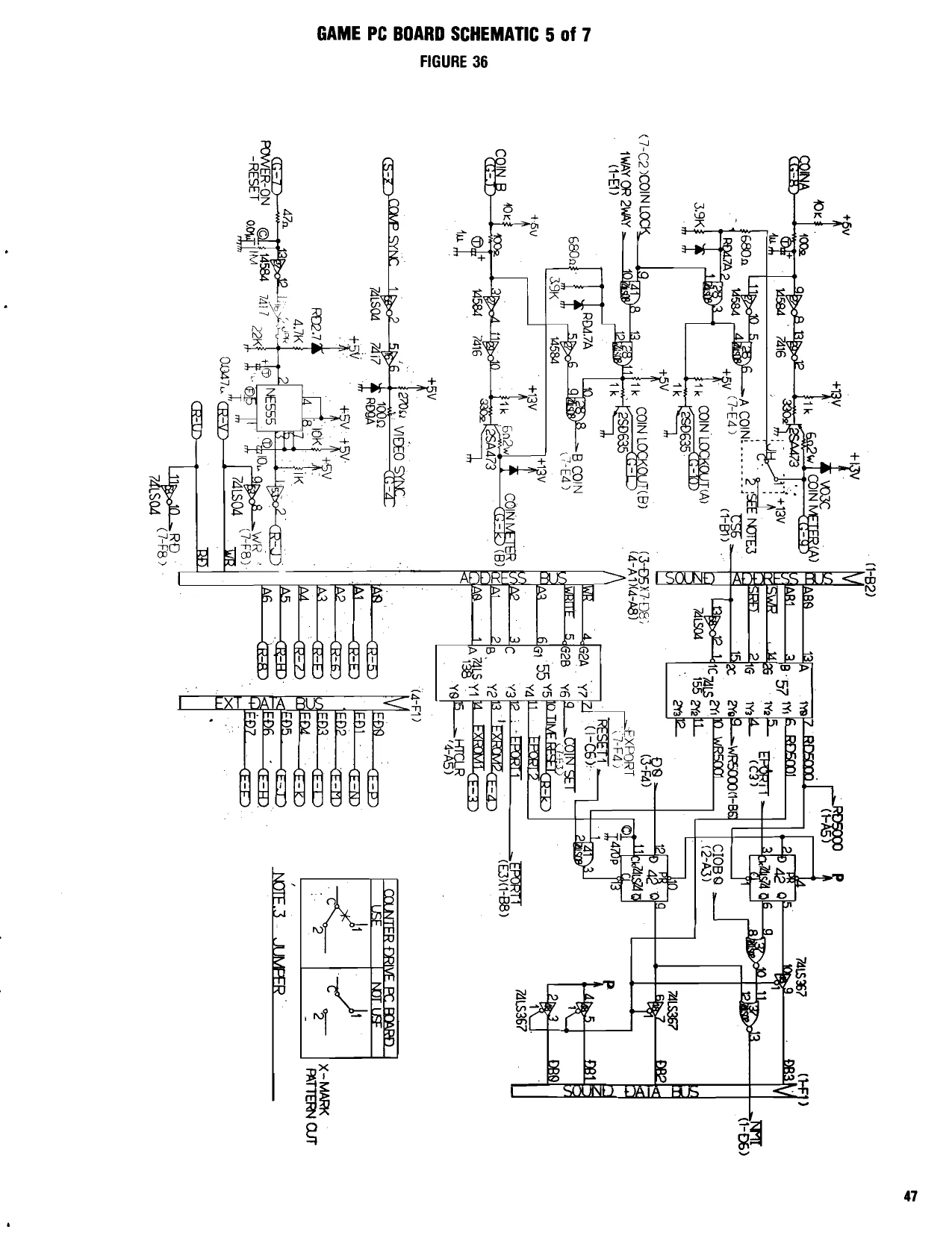
This page is a drawing, shown as the original scan.
This page is a drawing, shown as the original scan.
This page is a drawing, shown as the original scan.
WIRING DIAGRAM
CONTROL, PANEL
¥ || Monon ly PANEL "LIGHTING THSTRUCTION,
RANSFORMER 33 ay_ stereo 7H
=i. | 2n2055 5 a |
- HEAT Sink
ASSEMBLY
3anp St0-8L0 ae ID “458 ore 7"
T PRIMARY
NOTES
NOTES
\rarro/ ® TAITO AMERICA CORPORATION 1256 Estes Avenue, Elk Grove Village,,|L 60007 _ Telephone (312) 981-1000 Telex 25-3290