Pole Position SP-218 1st Printing
Pole Position (World) (Namco, 1982) · Schematic Package · 32 pages · 78 sections · original scan
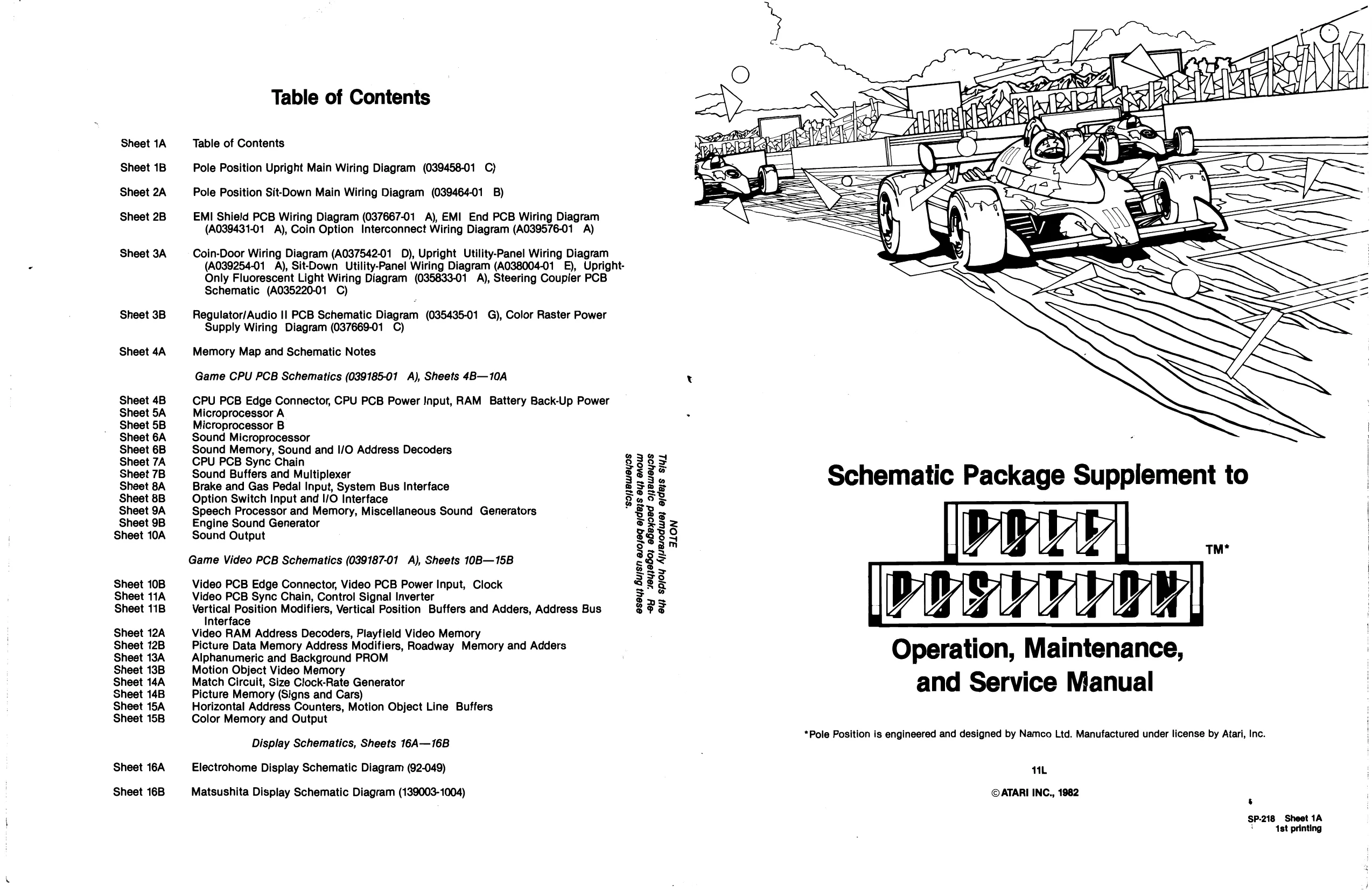
Sheet 1A
Sheet 1B
Sheet 2A
Sheet 2B
Sheet 3A
Sheet 3B
Sheet 4A
Sheet 4B Sheet 5A Sheet 5B Sheet 6A Sheet 6B Sheet 7A Sheet 7B Sheet 8A Sheet 8B Sheet 9A Sheet 9B Sheet 10A
Sheet 10B Sheet 11A Sheet 11B
Sheet 12A Sheet 12B Sheet 13A Sheet 13B Sheet 14A Sheet 14B Sheet 15A Sheet 15B
Sheet 16A
Sheet 16B Table of Contents ay NS
pan Table of Contents
Pole Position Upright Main Wiring Diagram (039458-01 C)
Pole Position Sit-Down Main Wiring Diagram (039464-01 B)
EMI Shield PCB Wiring Diagram (037667-01 A), EMI End PCB Wiring Diagram (A039431-01 A), Coin Option Interconnect Wiring Diagram (A039576-01 A)
Coin-Door Wiring Diagram (A037542-01 0), Upright Utility-Panel Wiring Diagram (A039254-01 A), Sit-Down Utility-Panel Wiring Diagram (A038004-01 E), Upright: Only Fluorescent Light Wiring Diagram (035833-01 A), Steering Coupler PCB Schematic (A035220-01 C)
Regulator/Audio || PCB Schematic Diagram (035435-01 G), Color Raster Power Supply Wiring Diagram (037669-01 C)
Memory Map and Schematic Notes
Game CPU PCB Schematics (039185-01 A), Sheets 4B—10A x
CPU PCB Edge Connector, CPU PCB Power Input, RAM Battery Back-Up Power Microprocessor A . Microprocessor B Sound Microprocessor Sound Memory, Sound and I/O Address Decoders CPU PCB Sync Chain Sound Buffers and Multiplexer Brake and Gas Pedal Input, System Bus Interface Option Switch Input and I/O Interface Speech Processor and Memory, Miscellaneous Sound Generators Engine Sound Generator Sound Output “sojeWeYyoS esey) Bujsn asojaq afd} ay} eAOW
Game Video PCB Schematics (039187-01 A), Sheets 10B—15B
Video PCB Edge Connector, Video PCB Power Input, Clock Video PCB Sync Chain, Control Signal Inverter Vertical Position Modifiers, Vertical Position Buffers and Adders, Address Bus Interface Video RAM Address Decoders, Playfield Video Memory . 7 Picture Data Memory Address Modifiers, Roadway Memory and Adders Aiphanumeric and Background PROM Operation, Maintenance, lotion Object Video Memory . Match Circuit, Size Clock-Rate Generator Se Picture Memory (Signs and Cars) and rvice Manual Horizontal Address Counters, Motion Object Line Buffers Color Memory and Output -ey 1943060; eGeyoed ojeweyos ey) spjoy Ajesoduie) ejdes sjyt
310N
. 5 “Pole Position is engineered and designed by Namco Ltd. Manufactured under license by Atari, Inc. Display Schematics, Sheets 16A—16B
Electrohome Display Schematic Diagram (92-049) 11L
Matsushita Display Schematic Diagram (139003-1004) ©ATARI INC., 1982 ‘
SP-218 Sheet 1A
- "48t printing
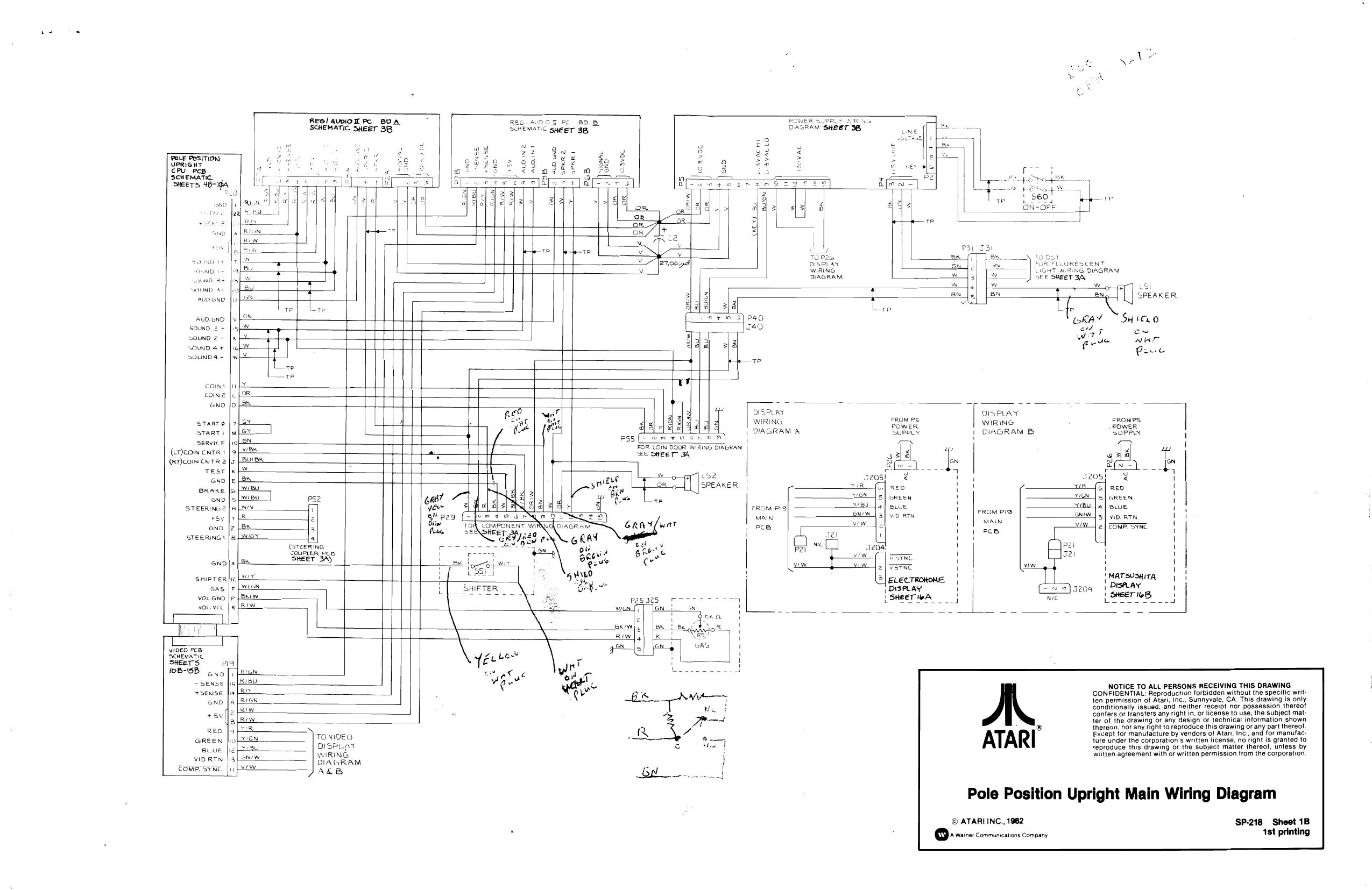
This page is a drawing, shown as the original scan.
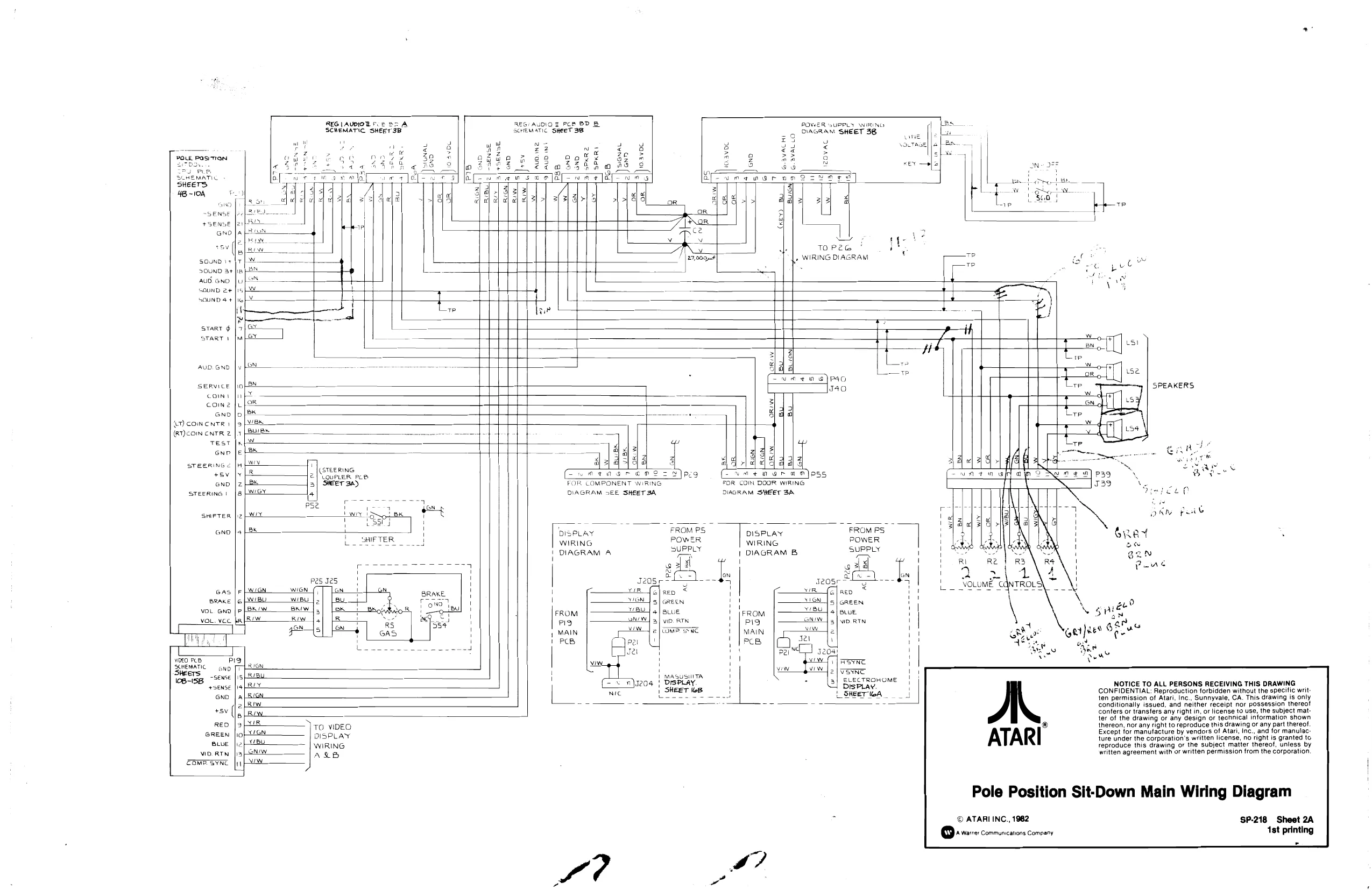
This page is a drawing, shown as the original scan.
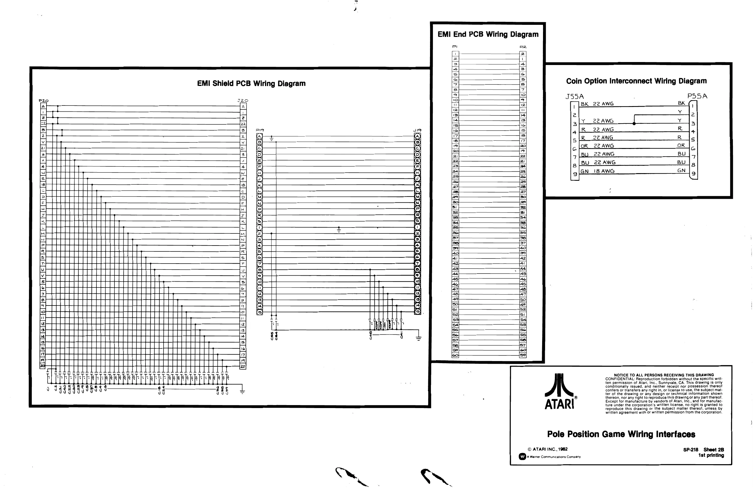
This page is a drawing, shown as the original scan.
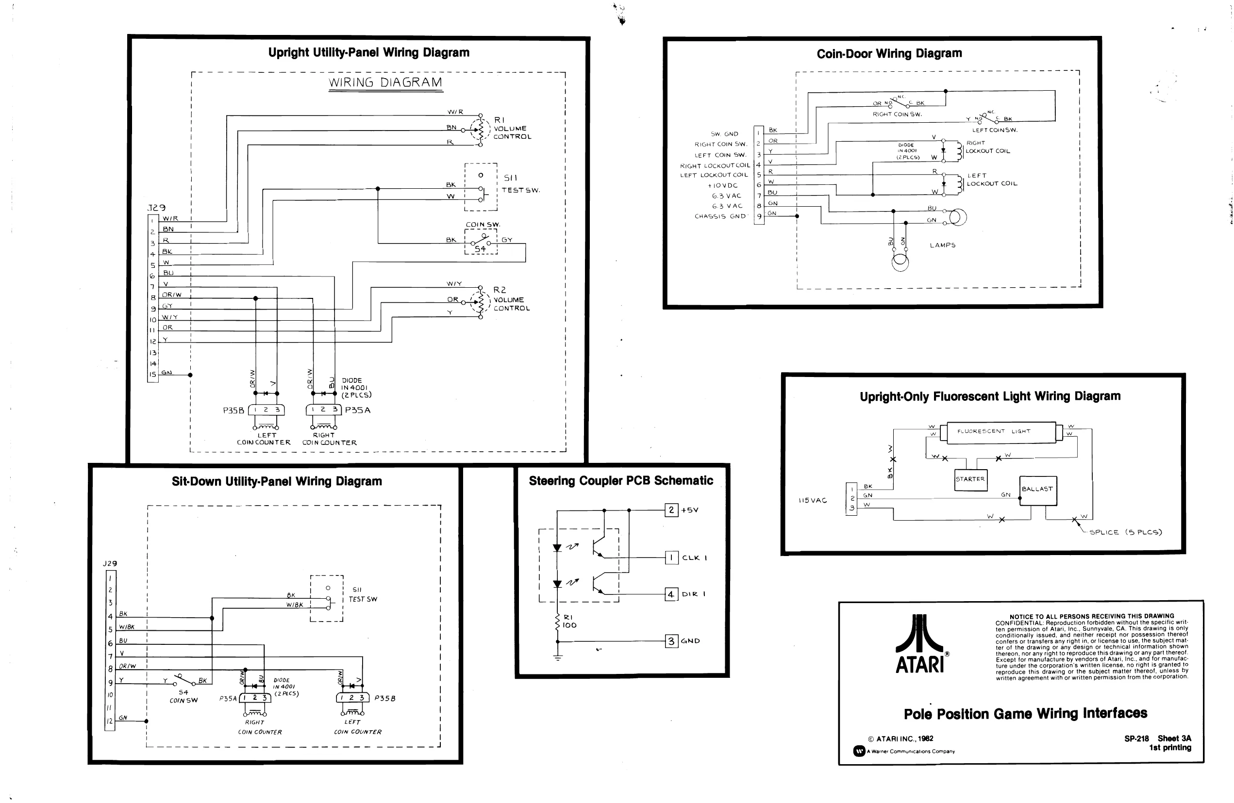
Upright Utility-Panel Wiring Diagram
WIRING DIAGRAM
poo c cc tcc o-oo 225 2-2-2 2-3-2 5-5-5 +55 ----
su TEST SW.
2 3
‘OO! rt (2PLcs) P35B(! 2 3) (2 3)Pa5a
bamd LEFT RIGHT COINCOUNTER COIN COUNTER,
RIGHT
COIN COUNTER 7 CONTROL ‘\ VOLUME ‘9W. GND.
RIGHT COIN SW
LEFT COIN SW,
RIGHT LOCKOUT COIL
LEFT LOCKOUT COIL,
+1OVDC
6.3 VAC
6.3 VAC
CHASSIS GND.
+5V
Coin-Door Wiring Diagram
RIGHT COIN Sw. ne oa ear
Bee RIGHT
wpcs)_W.
Lert LEFT COINSW.
inaoor [tocxour co”
| Lockour cone
Upright-Only Fluorescent Light Wiring Diagram
STARTER
MIS VAC
Ww FLUORESCENT LIGHT
Ce
BALLAST on
ATARI
- x SPLICE (5 PLCS)
NOTICE TO ALL PERSONS RECEIVING THIS DRAWING CONFIDENTIAL: Reproduction forbidden without the specific writ ten permission of Atari, Inc., Sunnyvale, CA. This drawing is only conditionally issued, and neither receipt nor possession thereot confers or transfers any right in, or license to use, the subject matter of the drawing or any design or technical information shown thereon, nor any right to reproduce this drawing or any part thereof. Except for manufacture by vendors of Atari, Inc., and for manufac: ture under the corporation's written license, no right is granted to reproduce this drawing or the subject matter thereof, unless by waitten agreement with or written permission from the corporation.
Pole Position Game Wiring Interfaces
© ATARI INC., 1982 SP-218 Sheet 3A ‘eccitatalad.
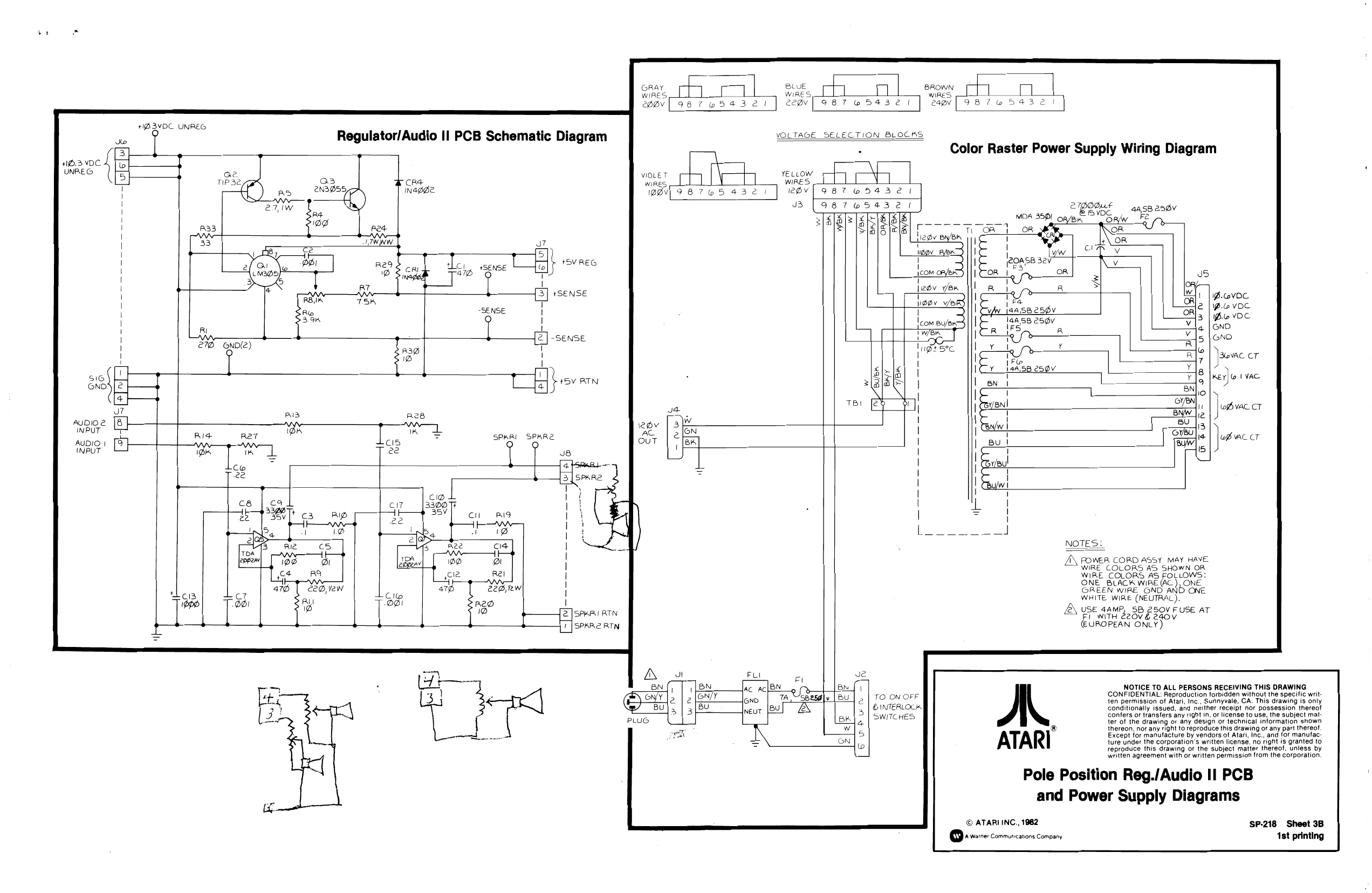
This page is a drawing, shown as the original scan.
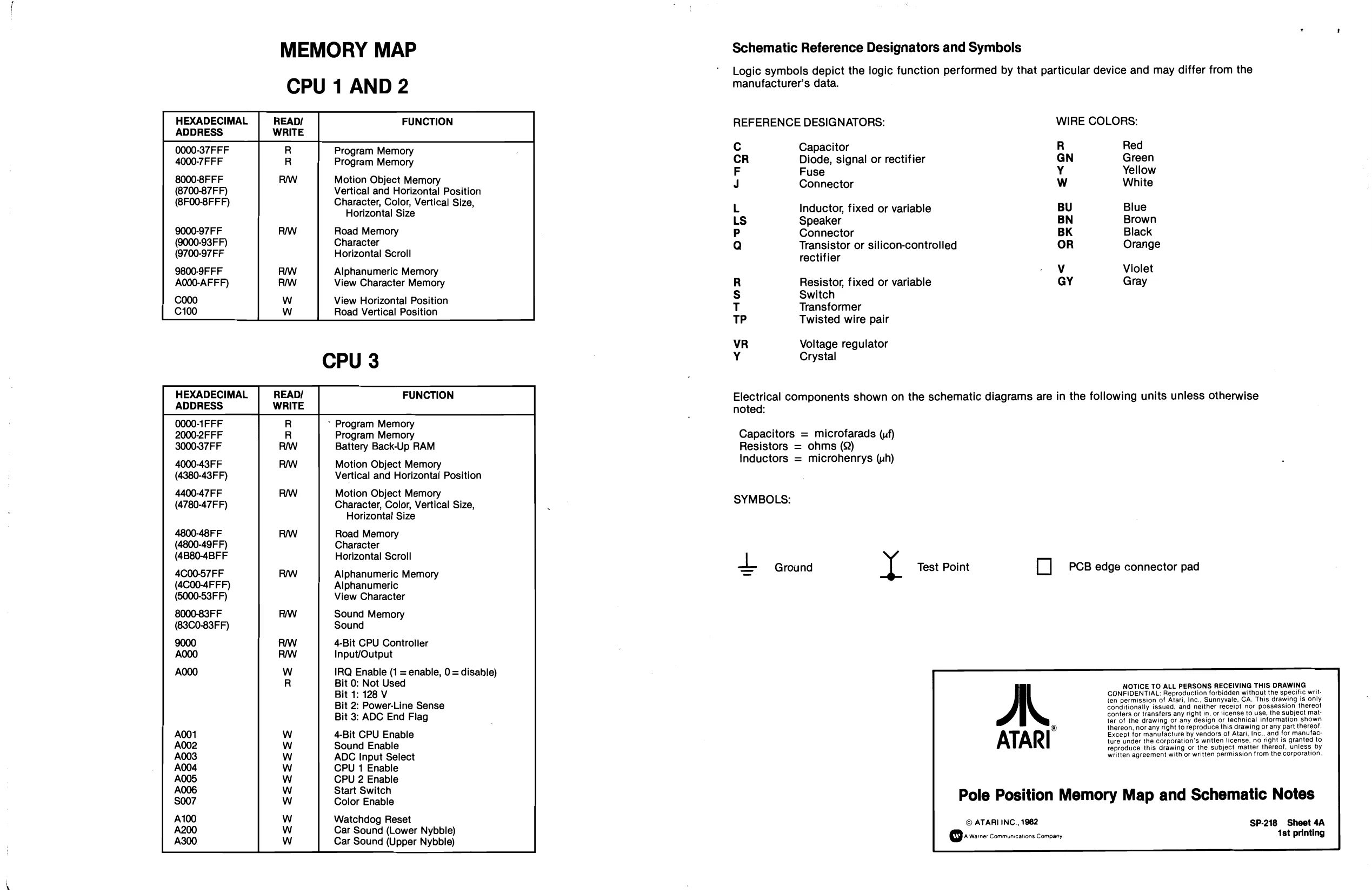
HEXADECIMAL ADDRESS
(0000-37FFF 4000-7 FFF 8000-8FFF (8700-87FF) (8F00-8F FF)
9000-97 FF (9000-93FF) (9700-97FF 9800-9FFF A000-AFFF) co0o C100
MEMORY MAP
CPU 1 AND 2
READ/ FUNCTION WRITE
Program Memory Battery Back-Up RAM Motion Object Memory
Vertical and Horizontal Position
Character, Color, Vertical Size,
Horizontal Size
Road Memory
Character Horizontal Scroll
Alphanumeric Memory View Character Memory
View Horizontal Position Road Vertical Position
0000-1FFF 2000-2FFF 3000-37FF
4000-43FF (4380-43FF) 4400-47 FF (4780-47FF)
4800-48FF (4800-49F F) (4880-4BFF 4C00-57FF (4C00-4FFF) (6000-53FF) 8000-83FF (83C0-83FF) 9000 A000 CPU 3
- Program Memory
Vertical and Horizontal Position
Horizontal Size
Character Horizontal Scroll
Alphanumeric View Character
Sound Memory Sound
4-Bit CPU Controller Input/Output IRQ Enable (1 = enable, 0 = disable) Bit 0: Not Used Bit 1: 128 V Bit 2: Power-Line Sense Bit 3: ADC End Flag 4-Bit CPU Enable Sound Enable ADC Input Select CPU 1 Enable CPU 2 Enable Start Switch Color Enable
Watchdog Reset Car Sound (Lower Nybble) Car Sound (Upper Nybble) Sse SSSSSS= Schematic Reference Designators and Symbols
Logic symbols depict the logic function performed by that particular device and may differ from the manufacturer's data.
REFERENCE DESIGNATORS: WIRE COLORS:
| c | Capacitor | R | Red |
| CR | Diode, signal or rectifier | GN | Green |
| F | Fuse | Y | Yellow |
| J | Connector | Ww | White |
| L | Inductor, fixed or variable | BU | Blue |
| Ls | Speaker | BN | Brown |
| P | Connector | BK | Black |
| Qa | Transistor or silicon-controlled | OR | Orange |
rectifier ov Violet
| R | Resistor, fixed or variable | GY | Gray |
Ss Switch T Transformer TP Twisted wire pair
Voltage regulator Crystal << az
Electrical components shown on the schematic diagrams are in the following units unless otherwise noted:
Capacitors = microfarads (uf) Resistors = ohms (Q) Inductors = microhenrys (uh)
SYMBOLS:
Lt Ground Test Point Oo PCB edge connector pad
NOTICE TO ALL PERSONS RECEIVING THIS DRAWING CONFIDENTIAL: Reproduction forbidden without the specific writ fen permission of Atari, Inc., Sunnyvale, CA. This drawing is only conditionally issued, and neither receipt nor possession thereof Confers or transfers any right in, or license to use, the subject matter of the drawing or any design or technical information shown ® thereon, nor any right to reproduce this drawing or any part thereof. Except for manufacture by vendors of Atari, Inc., and for manufac: ture under the corporation's written license, no right is granted to reproduce this drawing or the subject matter thereof, unless by written agreement with or written permission from the corporation.
Pole Position Memory Map and Schematic Notes
© ATARI INC., 1962 SP-218 Sheet 4A Q dwarves communcarions Company 1st printing
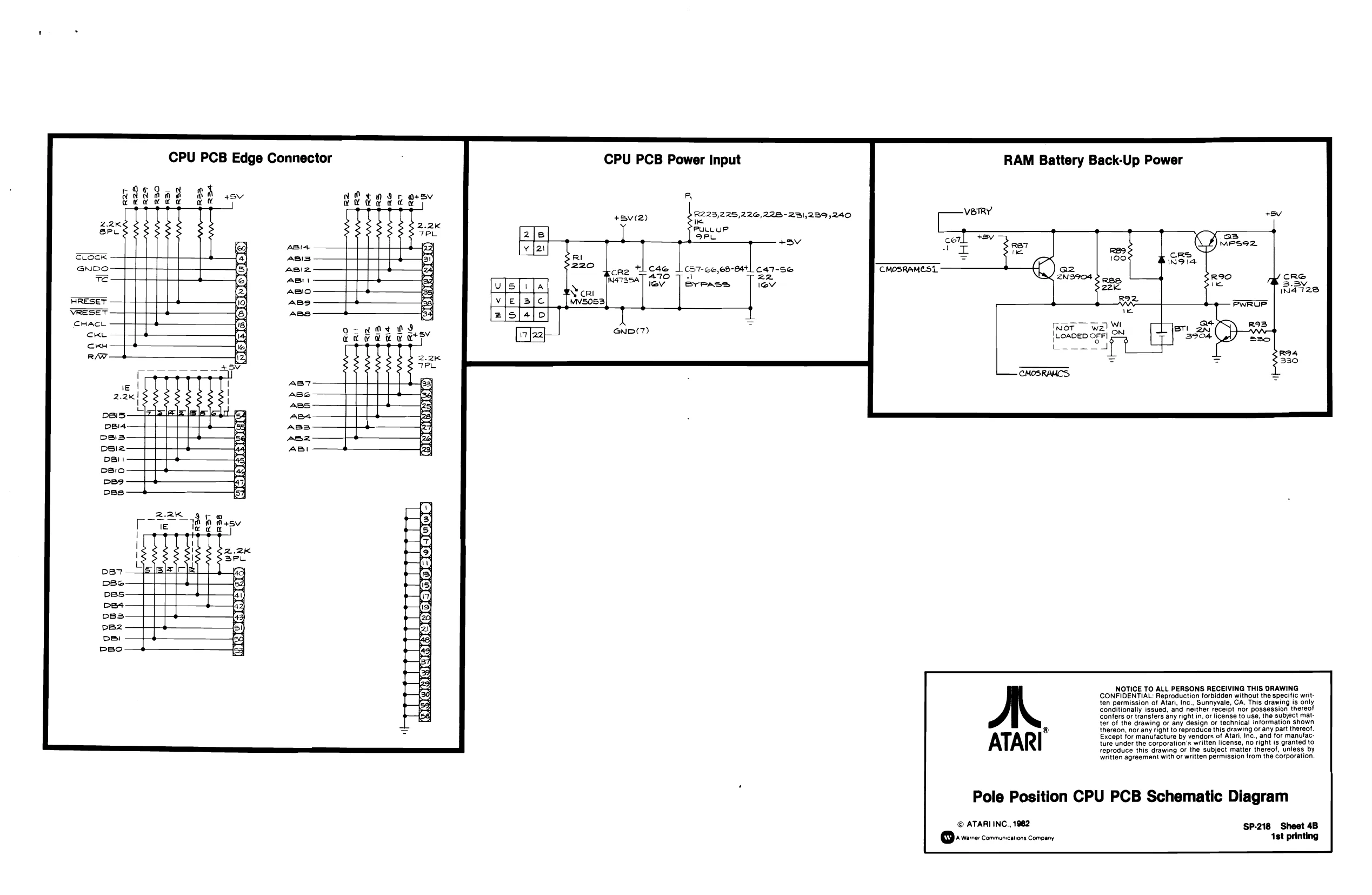
This page is a drawing, shown as the original scan.
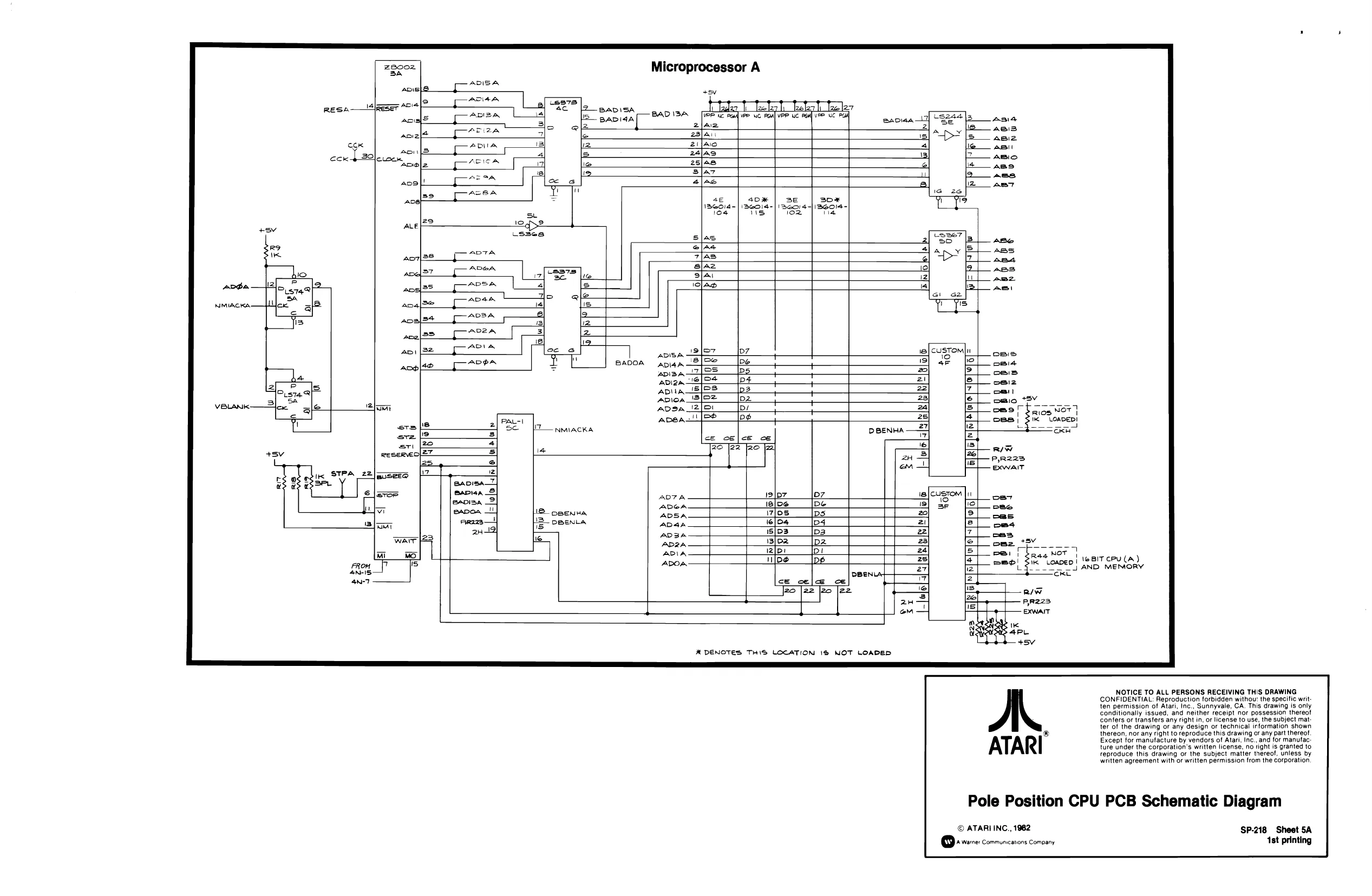
Microprocessor A
+5v
fi 7h laele7 [aa7|
S55 4] “DY
in
ez aun
CUSTOM 10) ae
[2— nmiacka DBENHA REP SA TETO ToT o7 0
a
HE oBeNHa
[3 DeeNLA 13 bee
ie +sv HF--<5-7 per uot Snag NOT | ! | Weert ceula) RRP, FIR LOADED | AND MEMORY 7c
Rw RyR2z3 exwart
ne 4PL +5v
- DENOTES THIS LOCATION 1S NOT LOADED
NOTICE TO ALL PERSONS RECEIVING THIS DRAWING
CONFIDENTIAL: Reproduction forbidden without the specific writ,
ten permission of Atari, Inc., Sunnyvale, CA. This drawing is only conditionally issued, and neither receipt nor possession thereof confers or transters any right in, or license to use, the subject mat. ter of the drawing or any design or technical irformation shown ® thereon, nor any right to reproduce this drawing or any part thereof. Except for manufacture by vendors of Atari, Inc., and for manutac: ture under the corporation's written license, no right is granted to reproduce this drawing or the subject matter thereof, unless by written agreement with or written permission from the corporation,
Pole Position CPU PCB Schematic Diagram
ATARI INC., 1982 SP-218 Sheet 5A Qo verre: Commune ons Company 1st printing
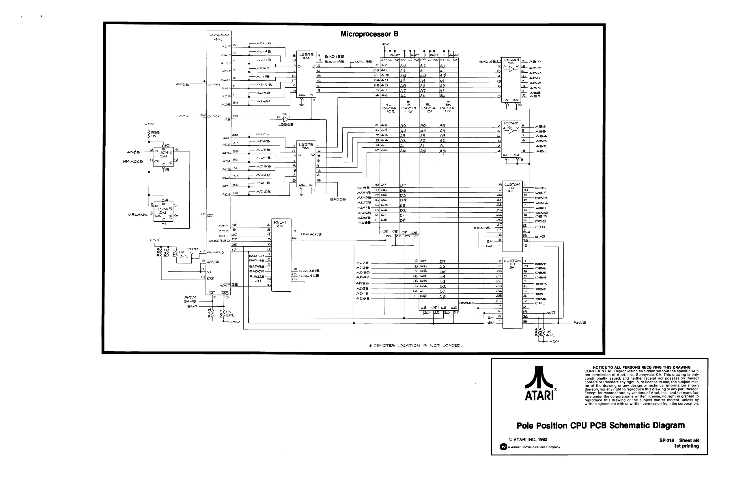
Microprocessor B
2 BaDisSB 12 2B 2 BADGE ee 2 le A f ig Ad 1B AT o VP ue Pau]
aL \Beoiato
As Aa
apes
NMIACKB
CUSTOM i) 4H
custom ite} 3H LS DBENHS: 13 OBENLE
% DENOTES LOCATION 1S NOT LOADED
NOTICE TO ALL PERSONS RECEIVING THIS DRAWING CONFIDENTIAL: Reproduction forbidden without the specific writ. ten permission of Atari, Inc., Sunnyvale, CA. This drawing is only conditionally issued, and neither receipt nor possession thereof confers or transfers any right in, or license to use, the subject matter of the drawing or any design or technical information shown ® thereon, nor any right to reproduce this drawing or any part thereof. Except for manufacture by vendors of Atari, Inc., and for manutacture under the corporation's written license, no right is granted to reproduce this drawing or the subject matier thereof, unless by written agreement with or written permission from the corporation,
Pole Position CPU PCB Schematic Diagram
© ATARI INC., 1962 ‘SP-218 Sheet 5B > Warre: Communicators Company 1st printing
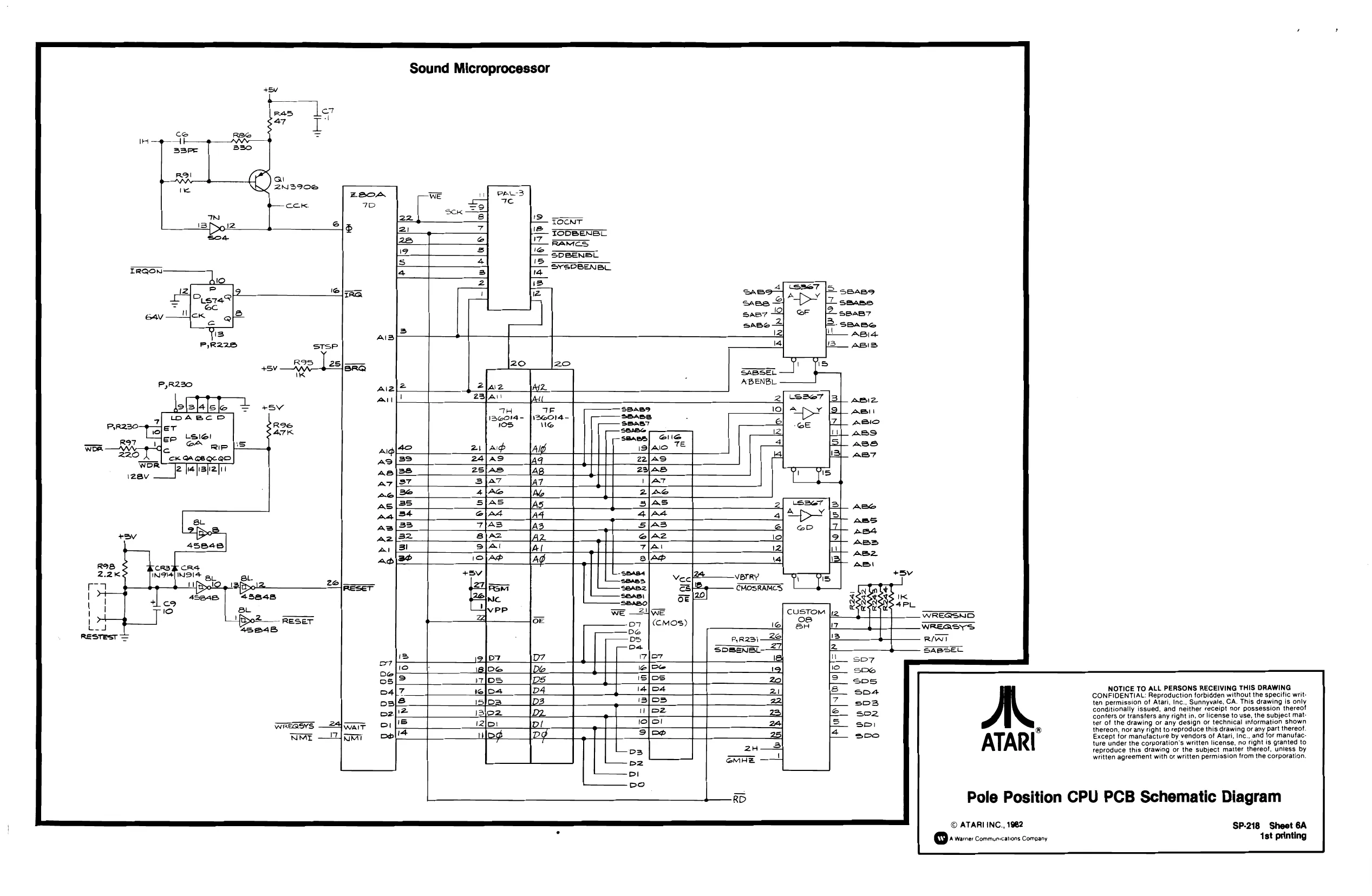
This page is a drawing, shown as the original scan.
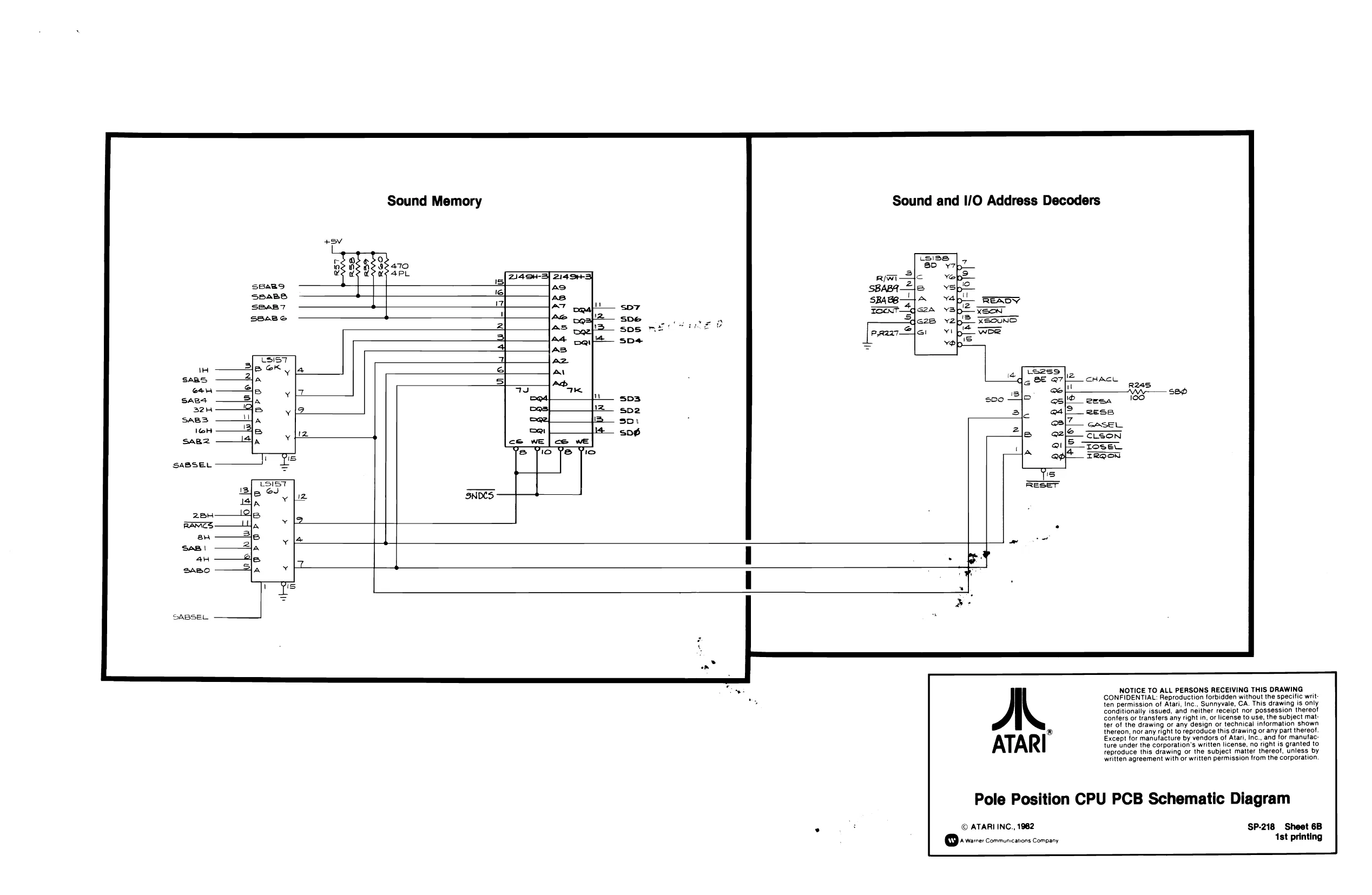
This page is a drawing, shown as the original scan.
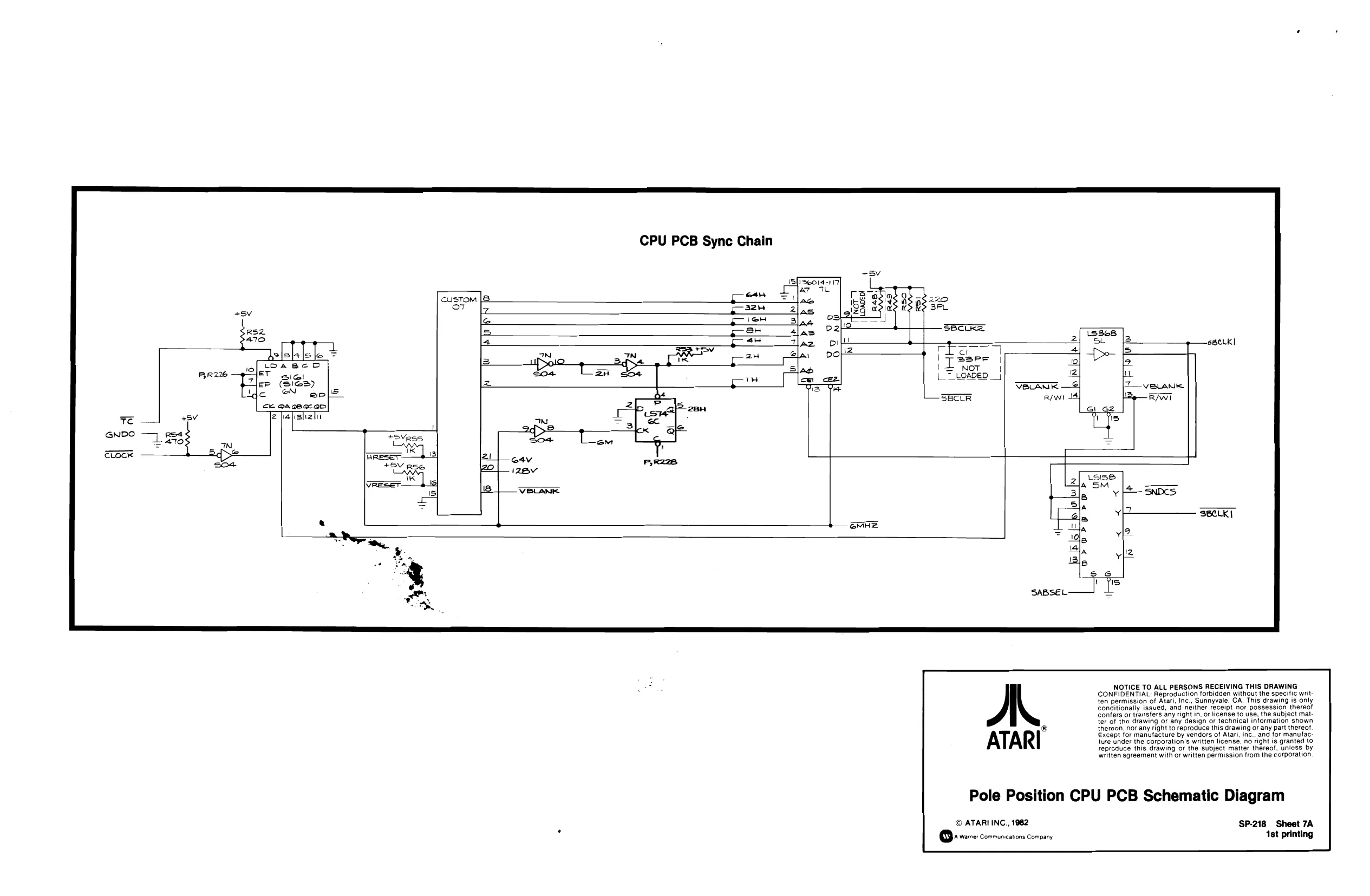
This page is a drawing, shown as the original scan.
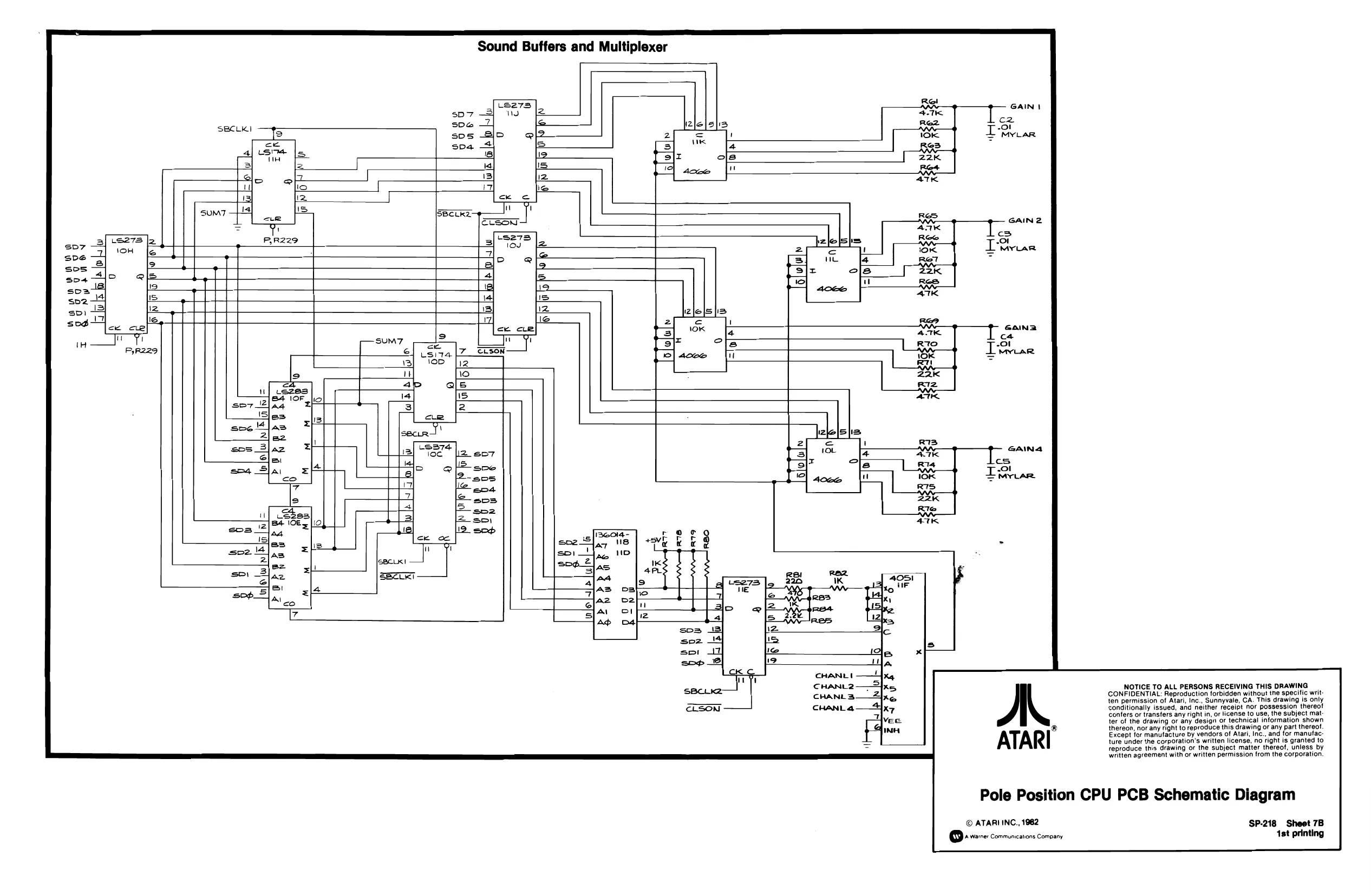
This page is a drawing, shown as the original scan.
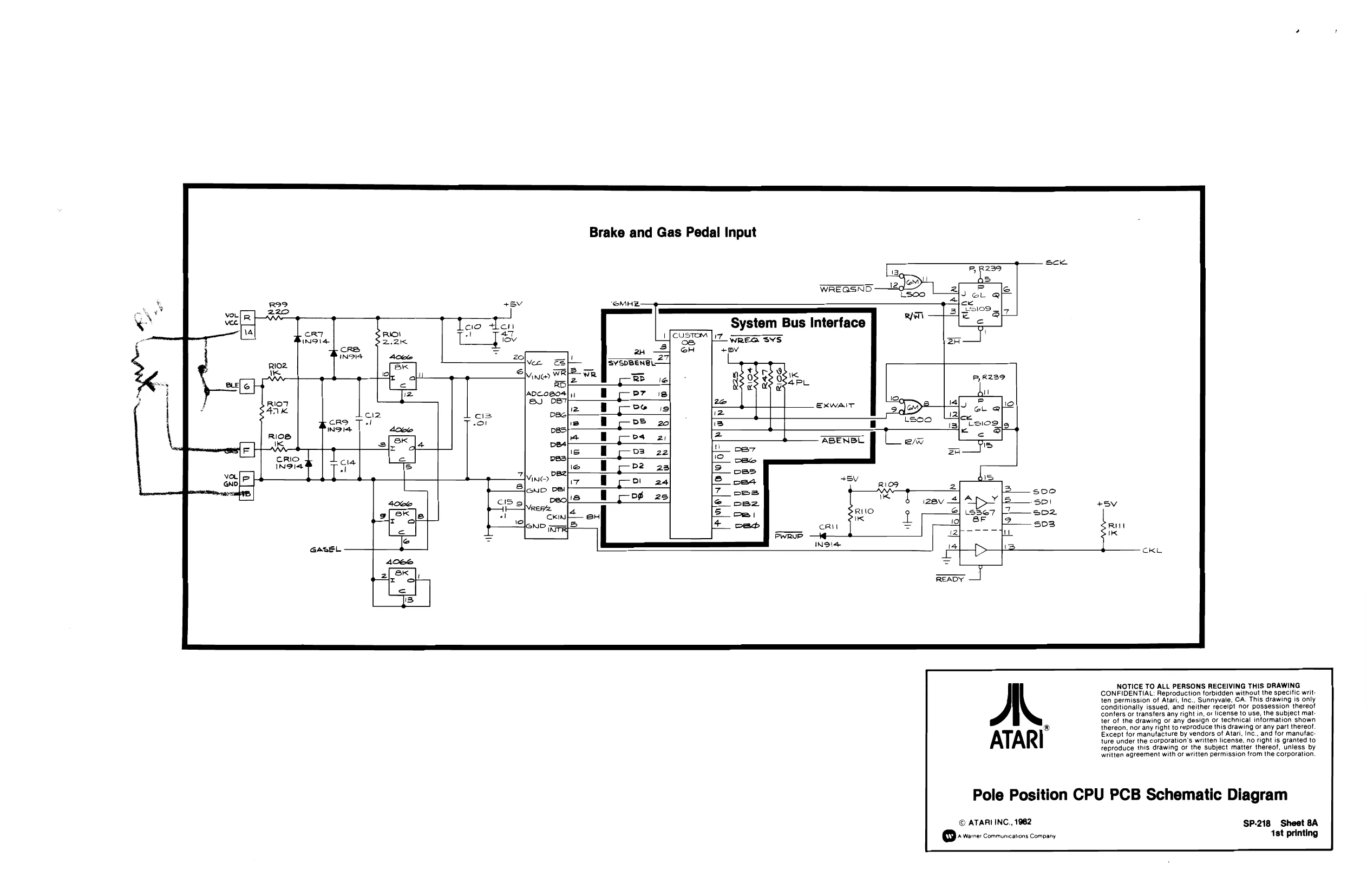
This page is a drawing, shown as the original scan.
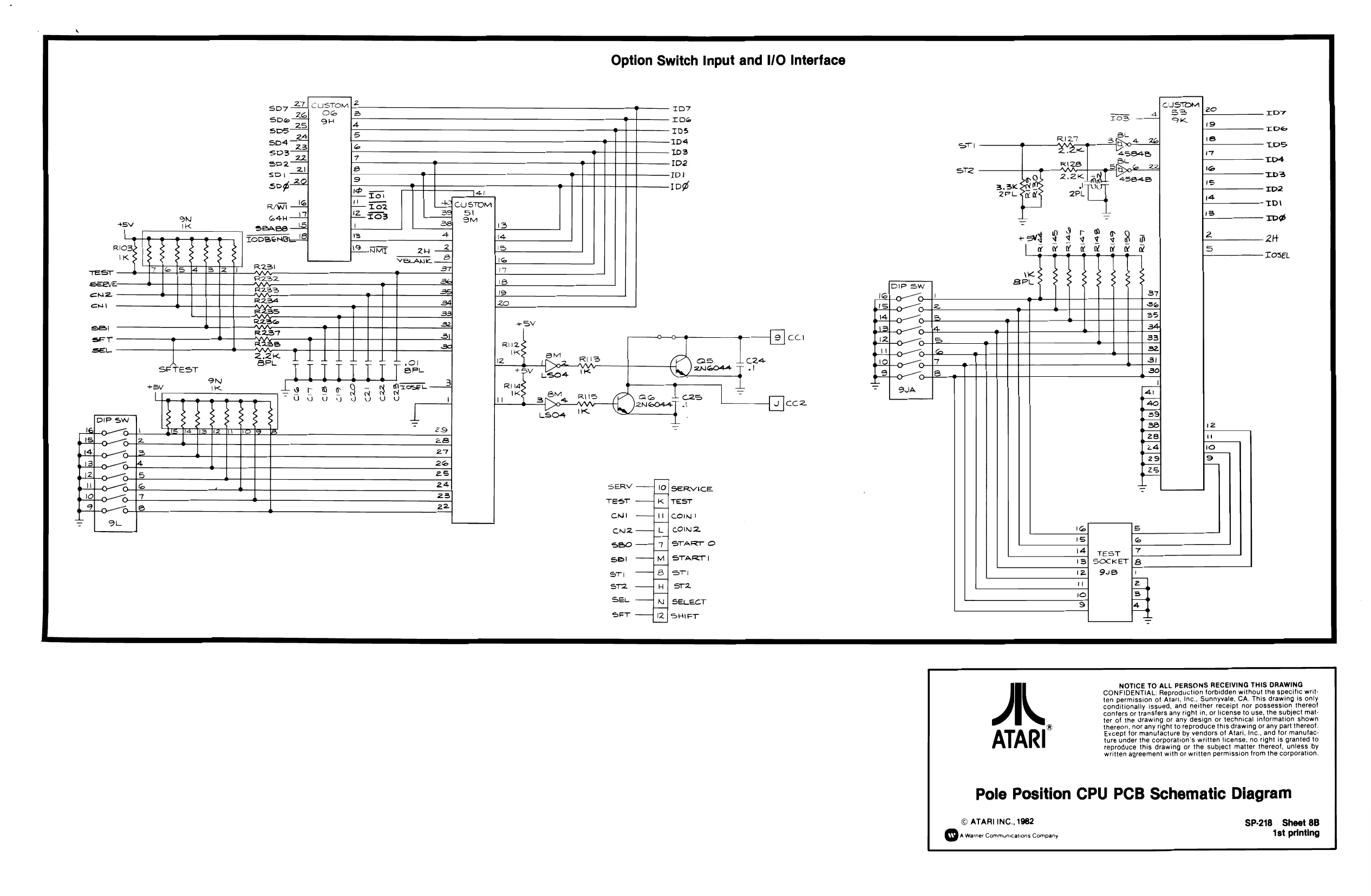
Option Switch Input and 1/O Interface
ROPERS
oan dy sence Topeensi Oo g
L__J R231
Rese
RSS
Rasa
Ss Rese
R257
S
2.2K yf ee fb Ue Uk A IY Joo bo 8
SERVICE
Test
CON!
COINZ
START O
START!
st
sr2
SeLecT
confers or transfers any right in, or license to use, the subject mat- NOTICE TO ALL PERSONS RECEIVING THIS DRAWING CONFIDENTIAL: Reproduction forbidden without the specific writ. ten permission of Atari, Inc., Sunnyvale, CA. This drawing is only conditionally issued, and neither receipt nor possession thereo!
ter of the drawing or any design or technical information shown ® thereon, nor any right to reproduce this drawing or any part thereof, Except for manufacture by vendors of Atari, Inc., and for manufac: ture under the corporation's written license, no right is granted to reproduce this drawing or the subject matter thereof, unless by written agreement with or written permission from the corporation.
Pole Position CPU PCB Schematic Diagram
© ATARI INC., 1982 SP-218 Sheet 8B > varre: Conmumeatons Company ‘1st printing
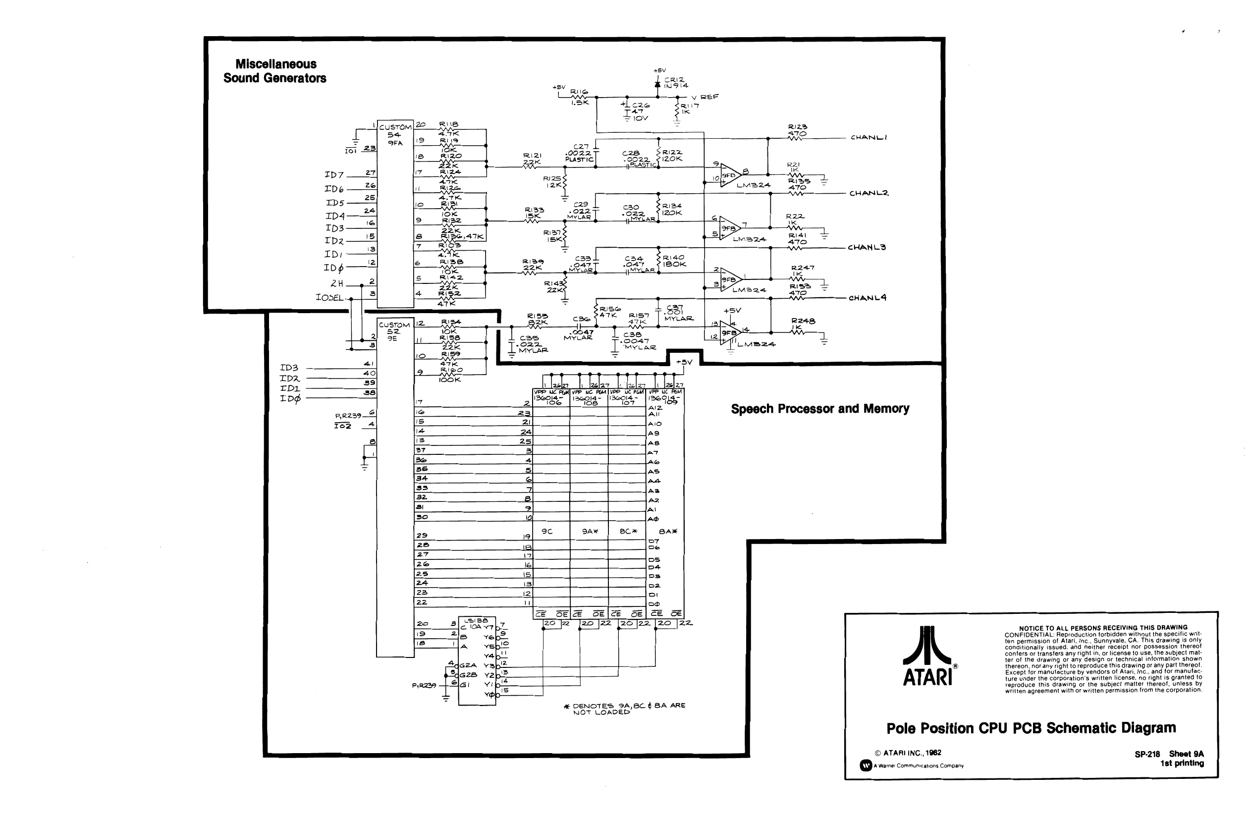
This page is a drawing, shown as the original scan.
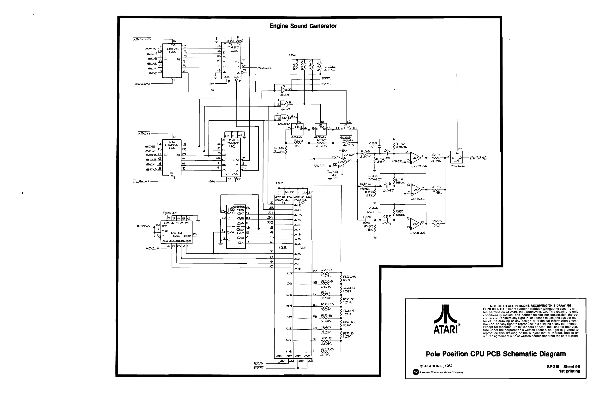
This page is a drawing, shown as the original scan.
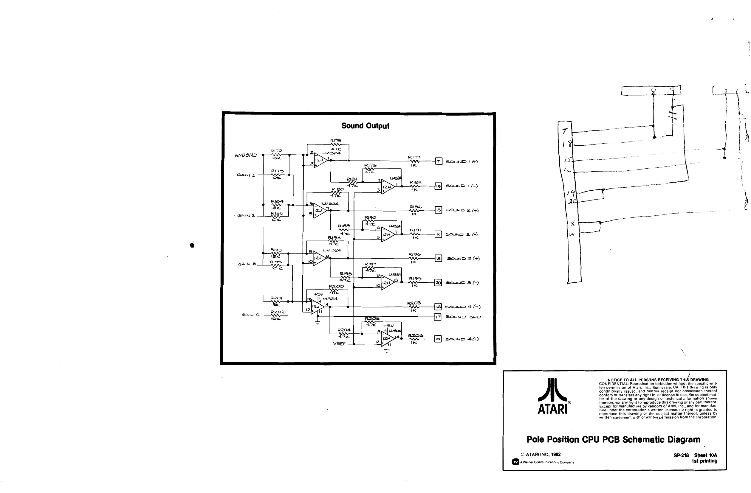
This page is a drawing, shown as the original scan.
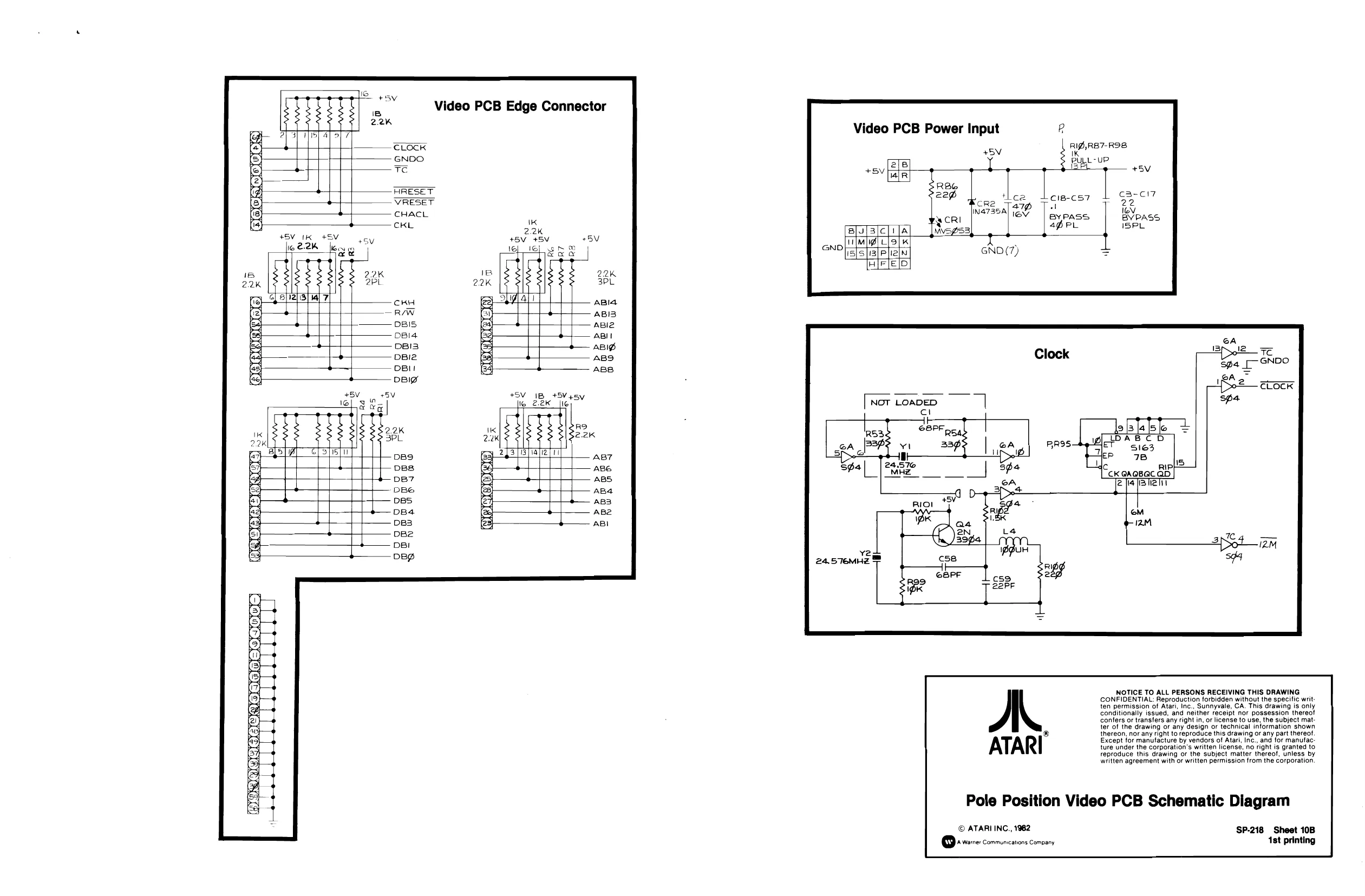
Video PCB Edge Connector
Video PCB Power Input R
RIP,RB7-ROB CLOCK 45V iD, GNDO TC IK PULL-UP Be
HRESET \ece7 VRESET nia
- CHACE BYPASS es ee apr +5V IK +SV
lows re a
NOT LOADED cl fk R53. C8PF Rs, Bags y, ag F 24.570 MHz
confers or transfers any right in, or license to use, the subject matter of the drawing or any design or technical information shown NOTICE TO ALL PERSONS RECEIVING THIS DRAWING CONFIDENTIAL: Reproduction forbidden without the specific writ: ten permission of Atari, Inc., Sunnyvale, CA. This drawing is only conditionally issued, and neither receipt nor possession thereot
® thereon, nor any right to reproduce this drawing or any part thereof. Except for manufacture by vendors of Atari, Inc., and for manufac: ture under the corporation's written license, no right is granted to reproduce this drawing or the subject matter thereof, unless by written agreement with or written permission from the corporation.
Pole Position Video PCB Schematic Diagram
© ATARI INC., 1962 SP-218 Sheet 10B + Wi2r26: Communications Company ‘1st printing
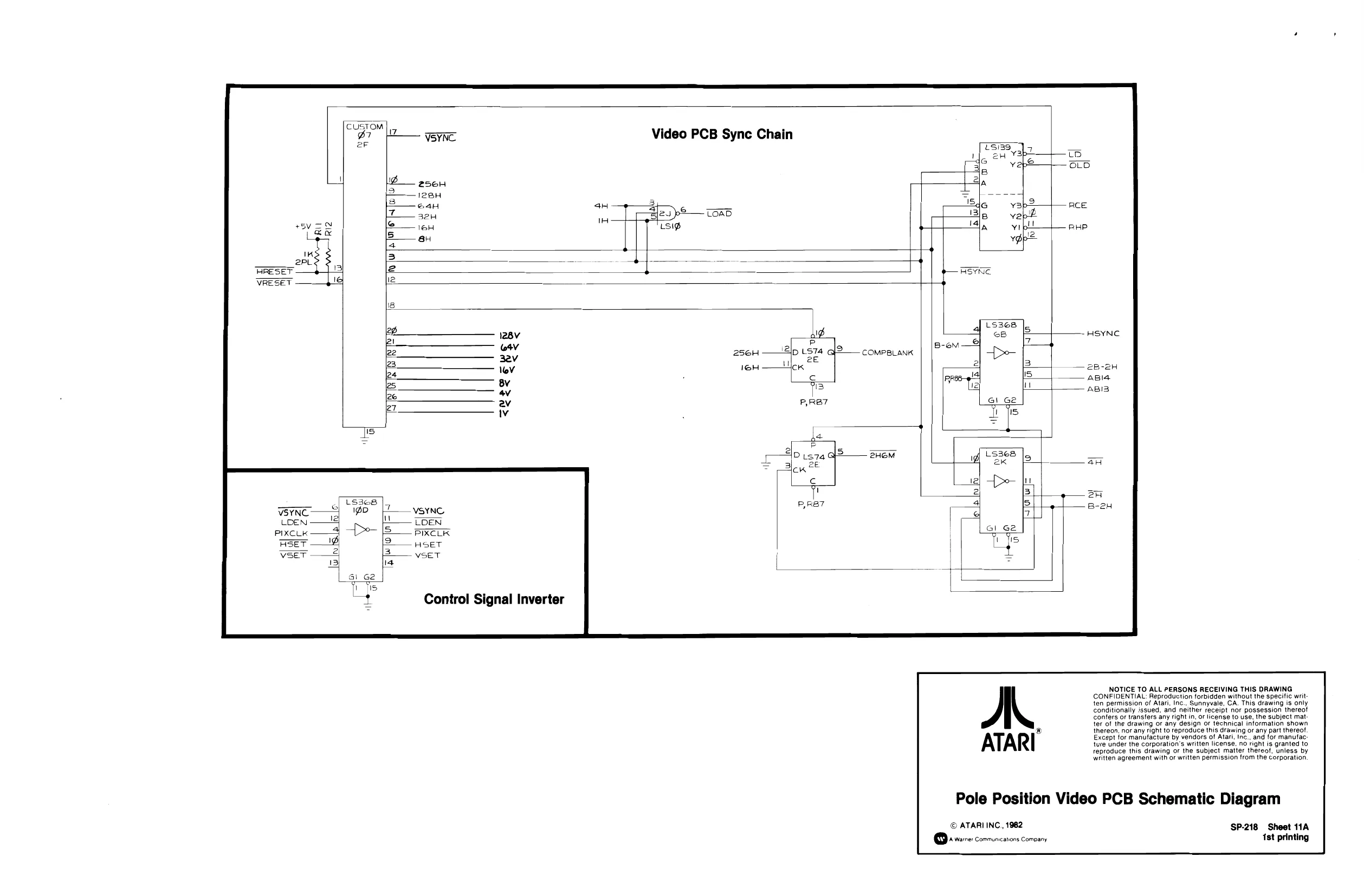
This page is a drawing, shown as the original scan.
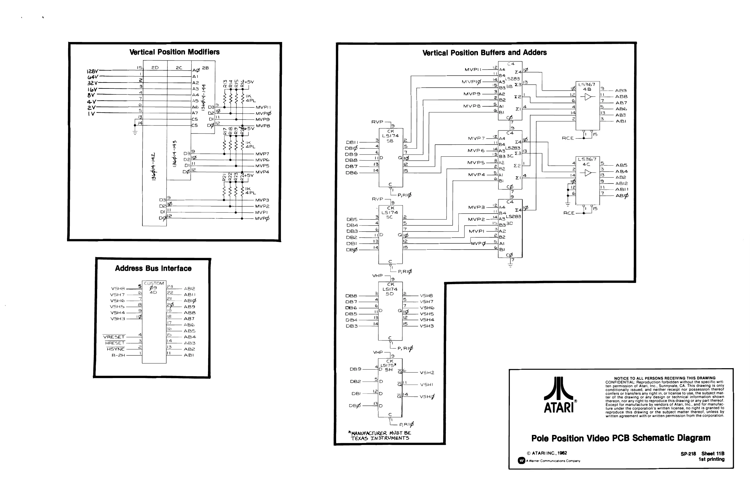
Vertical Position Modifiers
Vertical Position Buffers and Adders
a 15] 2D ac ~
| ag 28 | MvPit | 12} aa | Ip |
| 1 | tf | za |
3 AL PS 263
| Az | VPI | iat | ||||||
| 3 | rans | MVP | Ip | i5|*? =, =3/2 | 1s367 | |||
| 3 | at | Sea | BCS" | |e | ane | |||
| + | Dat | MvP2 | ae | lt | a] | pS | fu | pm |
| 2 | 5 | 2\pa | A | 7 | i | |||
| = | Ae a | MVP6 | Slay | xil4 | 4| | Is | i | |
| E | a7 | ele, | val | BT | ABS |
, cs. “ 7
120614 -1943,
Address Bus Interface
CUSTOM po 4D
VRESET HRESET HSYNC B-2H
NOTICE TO ALL PERSONS RECEIVING THIS DRAWING CONFIDENTIAL: Reproduction forbidden without the specific writ: ten permission of Atari, Inc., Sunnyvale, CA. This drawing is only Conditionally issued, and neither receipt nor possession thereof confers or transfers any right in, or license to use, the subject mat: ter of the drawing or any design or technical information shown thereon, nor any right to reproduce this drawing or any part thereo!. Except for manufacture by vendors of Atari, Inc., and for manufacture under the corporation's written license, no right is granted to reproduce this drawing or the subject matter thereof, unless by written agreement with or written permission from the corporation. A.
ATARI
i Lrg XMANUFACTURER MUST BE TEXAS INSTRUMENTS
Pole Position Video PCB Schematic Diagram
SP-218 Sheet 11B © ATARI INC., 1962
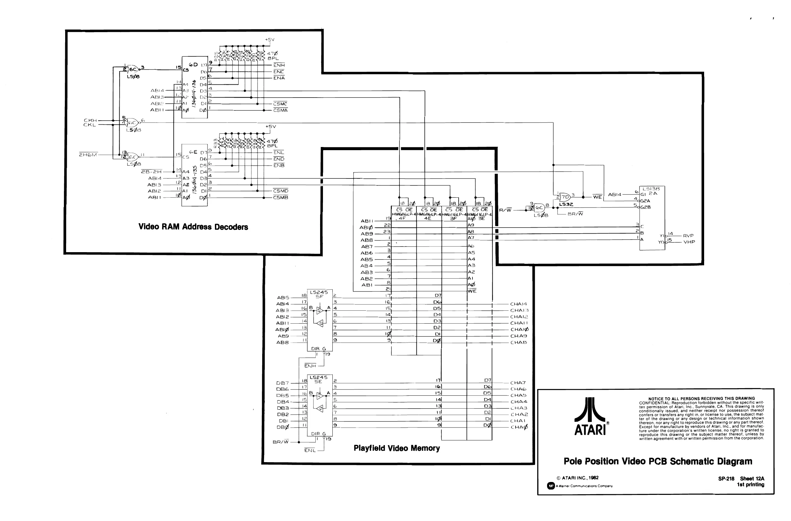
This page is a drawing, shown as the original scan.
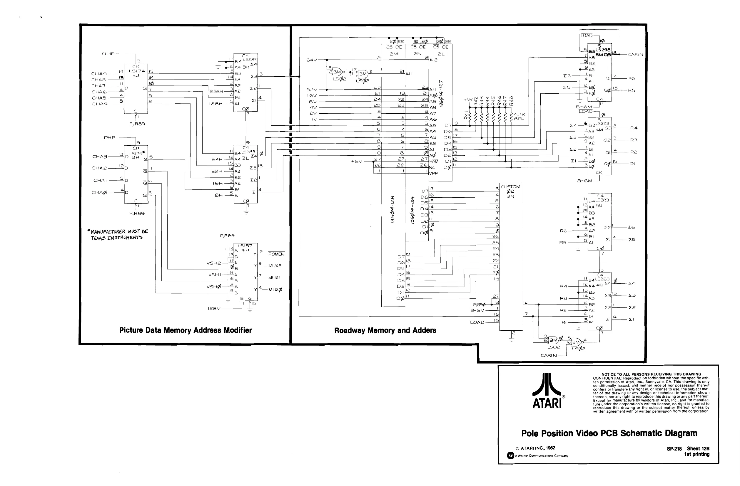
This page is a drawing, shown as the original scan.
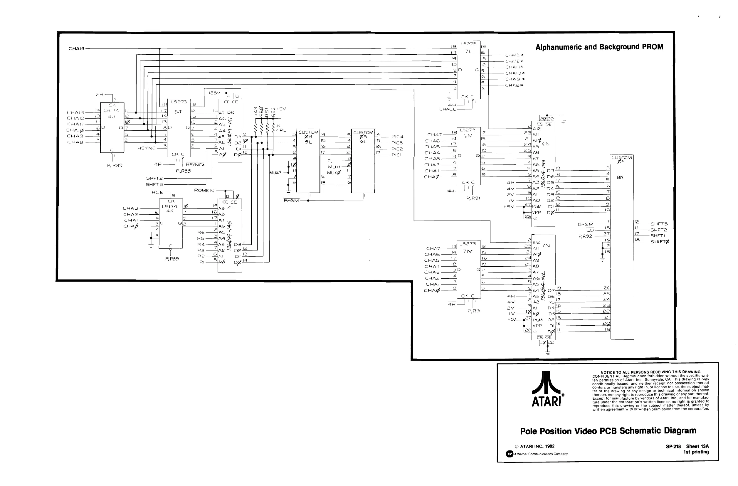
This page is a drawing, shown as the original scan.
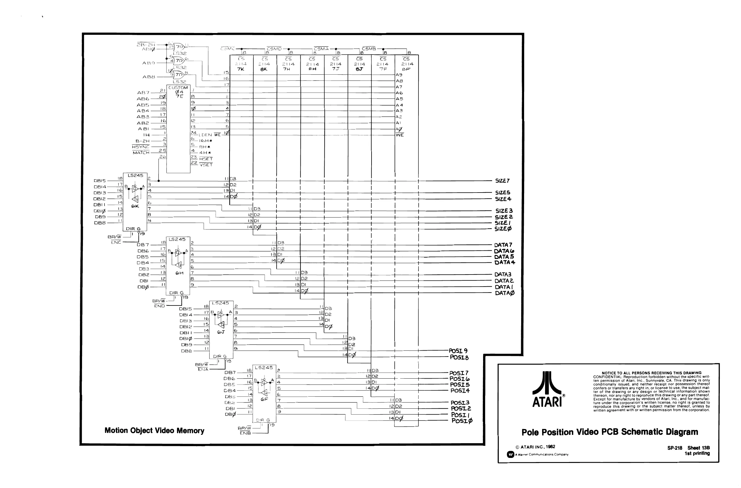
This page is a drawing, shown as the original scan.
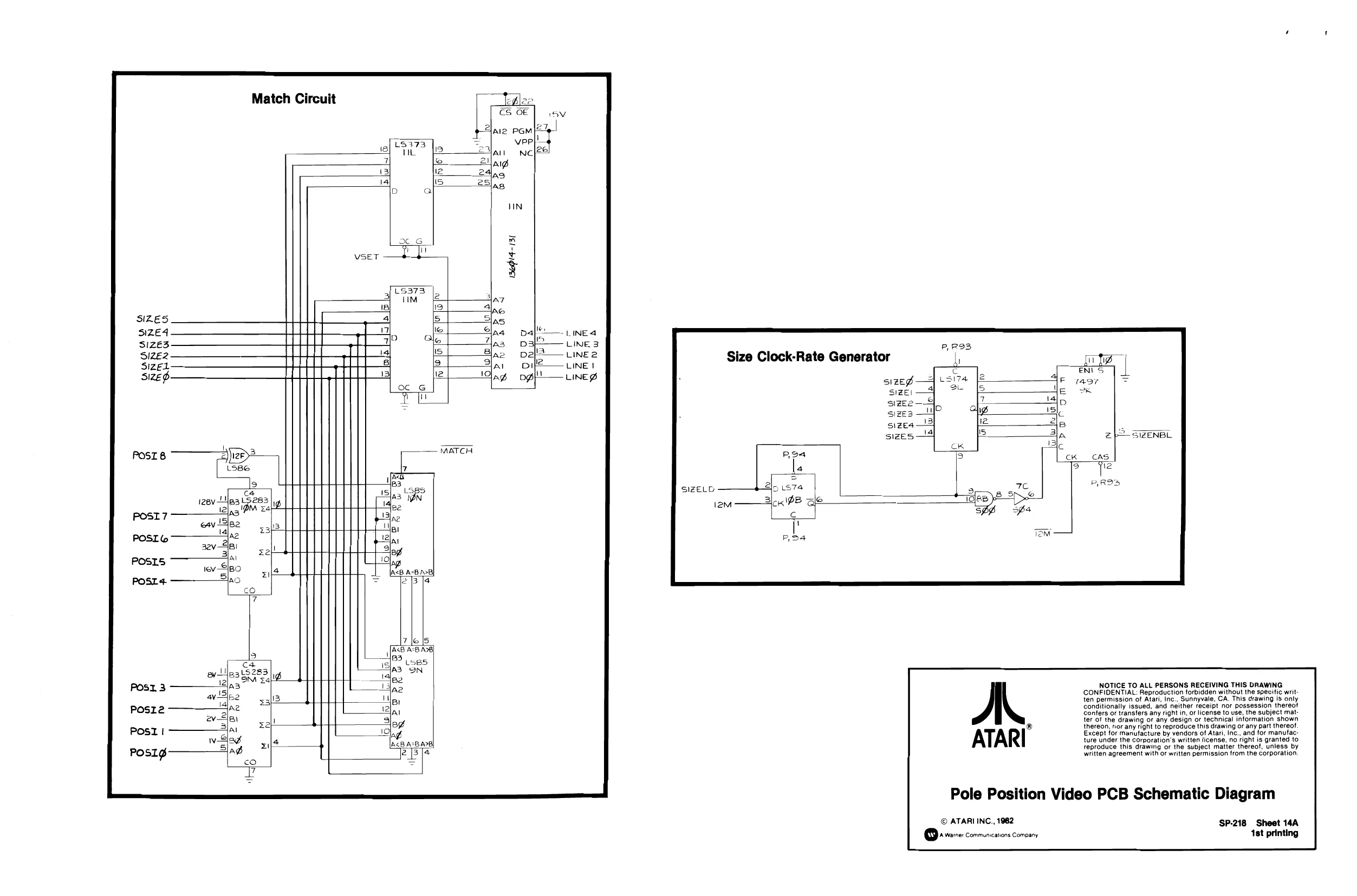
Match Circuit
Al Aig Aa AB Ale PGM vpp|!
NC
3 fo Joo LW Jo Jr fs [a
cB A-B Ara] 3 Ja
7 |e |5
BS
a3,
B2 a2 | ARBAB AB)
L585 QN
Size Clock-Rate Generator
sized SIZEI
size
SIZE4
SIZES
SIZELD oy
G
i
a SIZENBL I ] {il b
12M
Confers or transfers any right in, or license to use, the subject mat: NOTICE TO ALL PERSONS RECEIVING THIS DRAWING CONFIDENTIAL: Reproduction forbidden without the specific writ ten permission of Atari, Inc., Sunnyvale, CA. This drawing is only conditionally issued, and neither receipt nor possession thereot
ter of the drawing or any design or technical intormation shown
® thereon, nor any right to reproduce this drawing or any part thereot,
Except for manutacture by vendors of Atari, Inc., and for manufac: ture under the corporation's written {icense, no Tight is granted to reproduce this drawing or the subject matter thereof, unless by watten agreement with or written permission from the Corporation
Pole Position Video PCB Schematic Diagram
@:ATARI ING; 1982 SP-218 Sheet 14A Qi ware: communcanons Comoany 1st printing
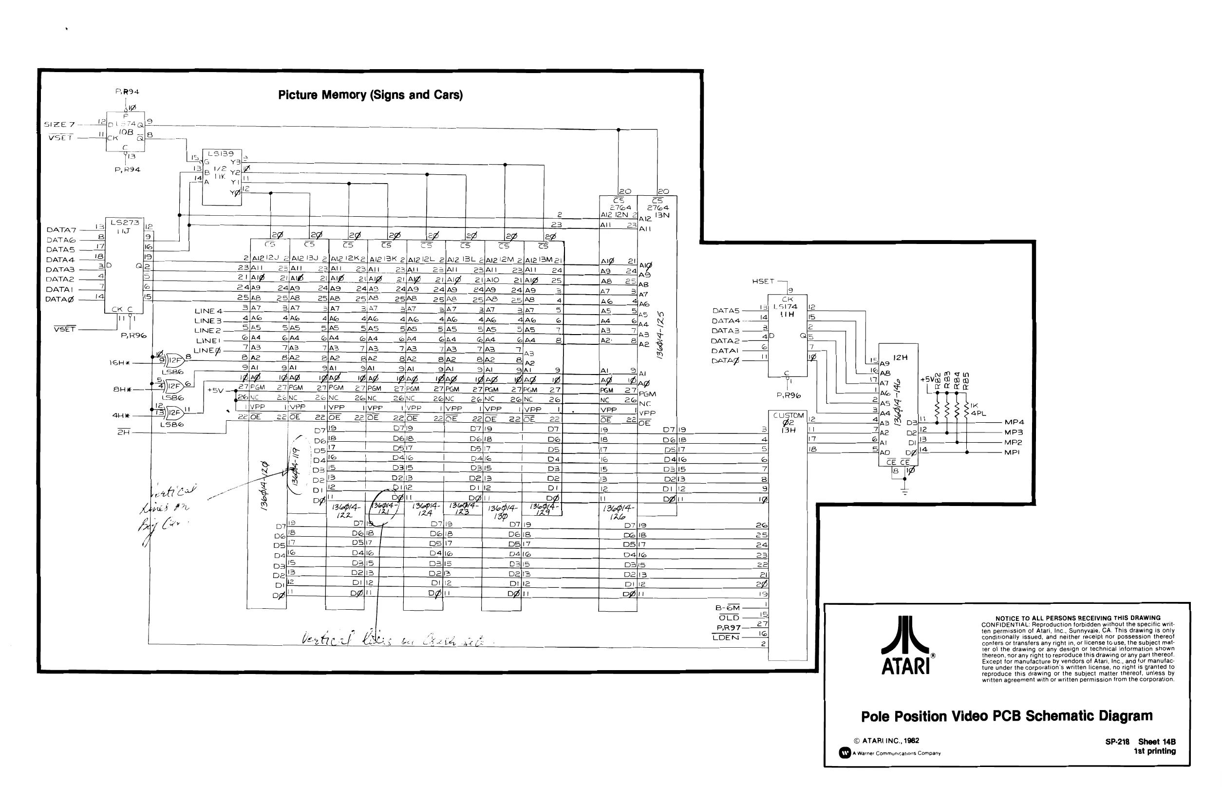
DATAS,
DaTaa DATAS DaATA2
DATAI DATAS
Picture Memory (Signs and Cars)
Jatt rats
o fx Ike
A212 Al2 [Bd 2 Iny Ap 2s/an Aa 13M ei} re Ap 2ilag 2 AS ny 24|a9 AZ. B [1s |w [o
25/48 ar AG
Veer LINE 4 LINE 3 LINE2
LINE!
LINED
BlA7. AS 4.AG aa S/S D3 Gad lon J for fur fin Jw
Aa: oo fs fo fox fo fw fin [3 |
Ta3 BiA2 glar Bidid (30bI4-/Z5 NP fos fo Jw lo fur fan fw
D719 pata —&| HSET
cK
- Loi7a [ie tal MH lis
3 2 aj a5
D
Delis
ps7 Dalic
Dslis bai
pi fiz $8 |v Joo [I Jura |
NOTICE TO ALL PERSONS RECEIVING THIS DRAWING CONFIDENTIAL: Reproduction forbidden without the specitic writ, ten permission of Atari, Inc., Sunnyvale, CA. This drawing is only Conditionally issued, and neither receipt nor possession thereof
confers or transfers any right in, or license touse, the subject mat
fer ol the drawing or any design or technical iniormation shown ® thereon, nor any right to reproduce this drawing or any part thereot Except for manufacture by vendors of Atari, Inc., and for manufac: ture Under the corporation's written license, no right is granted to reproduce this crawing or the subject matter thereof, uniess by wntten agreement with or written permission from the Corporation.
Pole Position Video PCB Schematic Diagram
© ATARI INC., 1982 ‘SP-218 Sheet 14B Qe ware: communcations Comoany 4st printing
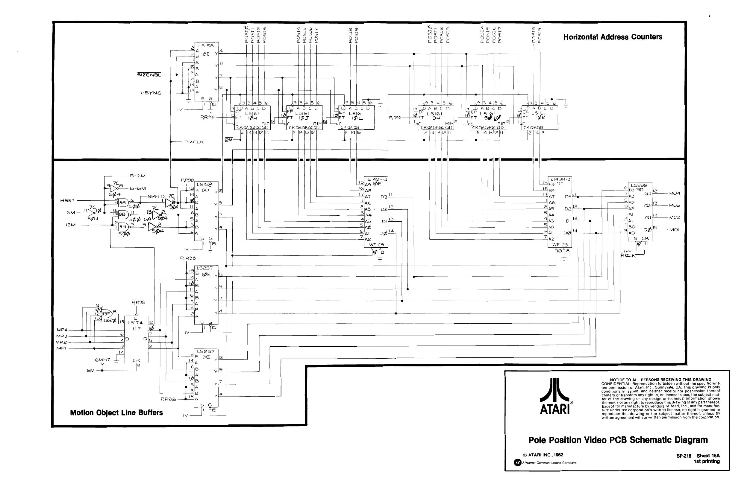
This page is a drawing, shown as the original scan.
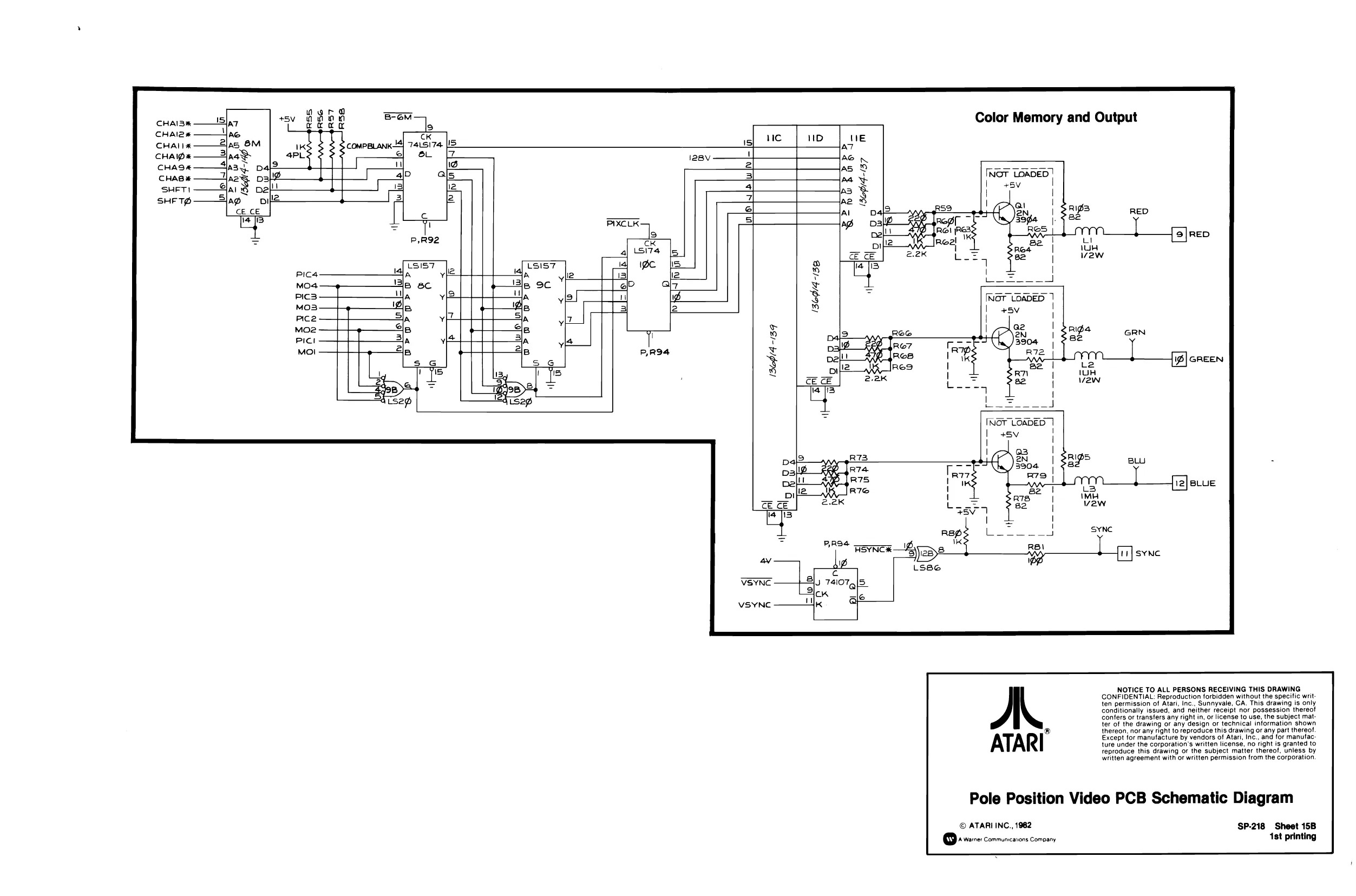
This page is a drawing, shown as the original scan.
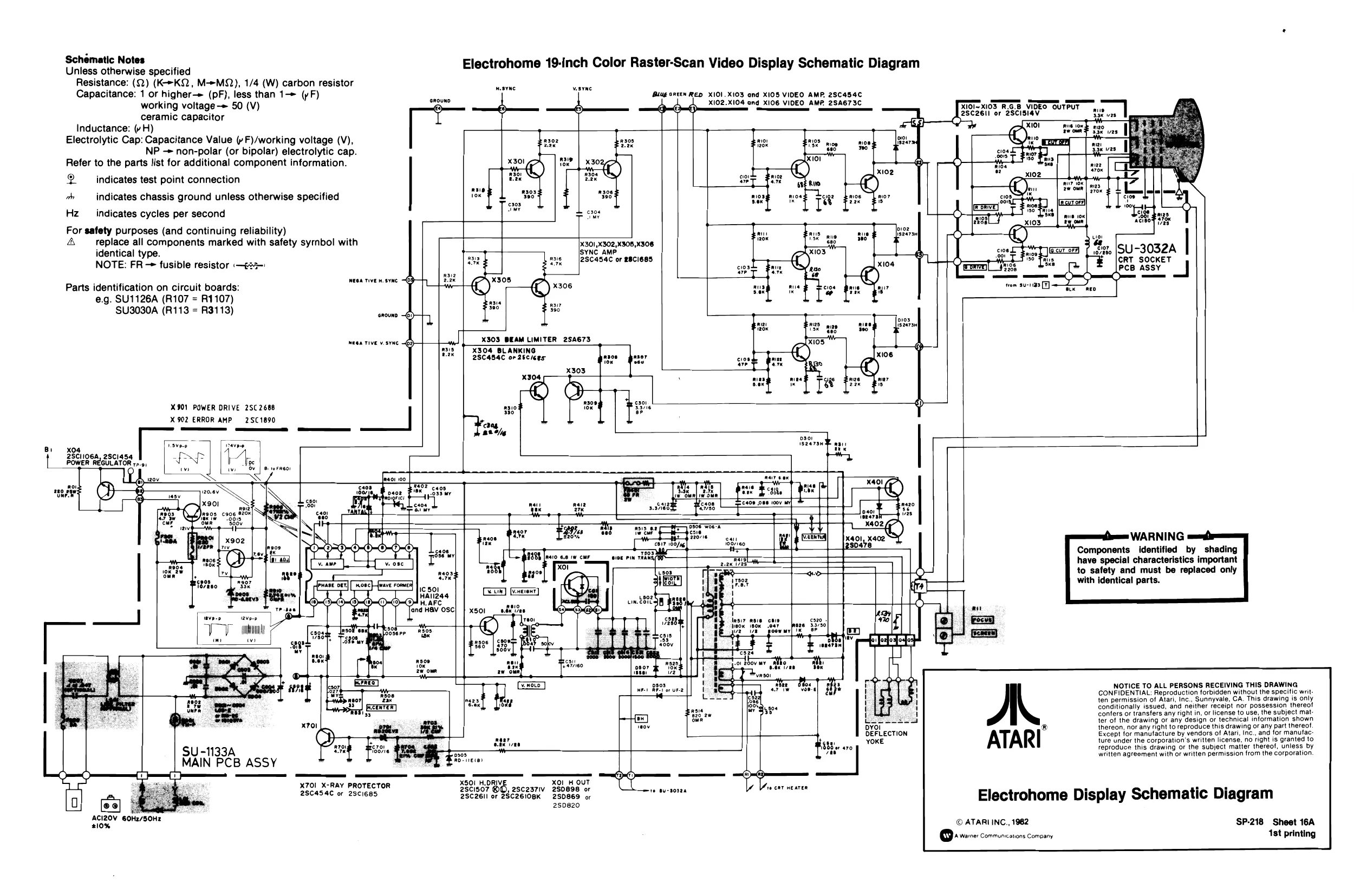
Schématic Notes
Unless otherwise specified Resistance: (22) (K->KQ, MM), 1/4 (W) carbon resistor Capacitance: 1 or higher—> (pF), less than 1 (yF) working voltage -> 50 (V) ceramic capacitor Inductance: (vH) Electrolytic Cap: Capacitance Value ( F)/working voltage (V), NP - non-polar (or bipolar) electrolytic cap. Refer to the parts list for additional component information. 2 indicates test point connection
ah indicates chassis ground unless otherwise specified
Hz _ indicates cycles per second For safety purposes (and continuing reliability) 4 replace all components marked with safety syrnbol with identical type.
NOTE: FR — fusible resistor ——es-'
Parts identification on circuit boards: e.g. SU1126A (R107 = R1107) $U3030A (R113 = R3113)
X901 POWER DRIVE 2SC 2668 X902 ERROR AMP — 2SC1890
Electrohome 19-inch Color Raster-Scan Video Display Schematic Diagram
Blug onten RED XIO1.X103 and X105 VIDEO AMP. 2SC454C XI02.X104 and X106 VIDEO AMP 2SA673C
301 ,X302,X308,x308
2SC454C or e8ci6es
X303 BEAM LIMITER 2SA673 X304 BLANKING 23C4B4C oF 26c/ces XIOl~X103 R.G.B VIDEO OUTPUT 2SC26Il or 2SCI514V
-3032A | RT SOCKET PcB ASSY |
VV eel mn wi
SU -1133A
MAIN PCB ASSY
& ACIZ0V 6OH2/50Hz 210% ‘WARNING Components identified by shading have special characteristics important to safety and must be replaced only with identical parts.
re:
X701_ X-RAY PROTECTOR 2SC454C or 2sci68s XO! HO ascas7iv 280898 NOTICE TO ALL PERSONS RECEIVING THIS DRAWING CONFIDENTIAL: Reproduction forbidden without the specific weit ten permission of Atari, Inc., Sunnyvale, CA. This drawing is only conditionally issued, and neither receipt nor possession thereo! confers or transfers any right in. or license to use, the subject mat: ter of the drawing or any design or technical information shown ® thereon, nor any right to reproduce this drawing or any part thereo!, Except for manufacture by vendors of Atari, Inc., and for manufac: ture under the corporation's written license, no right is granted to reproduce this drawing or the subject matter thereof, unless by written agreement with or written permission from the Corporation.
Electrohome Display Schematic Diagram
SP-218 Sheet 16A © ATARI INC., 1962
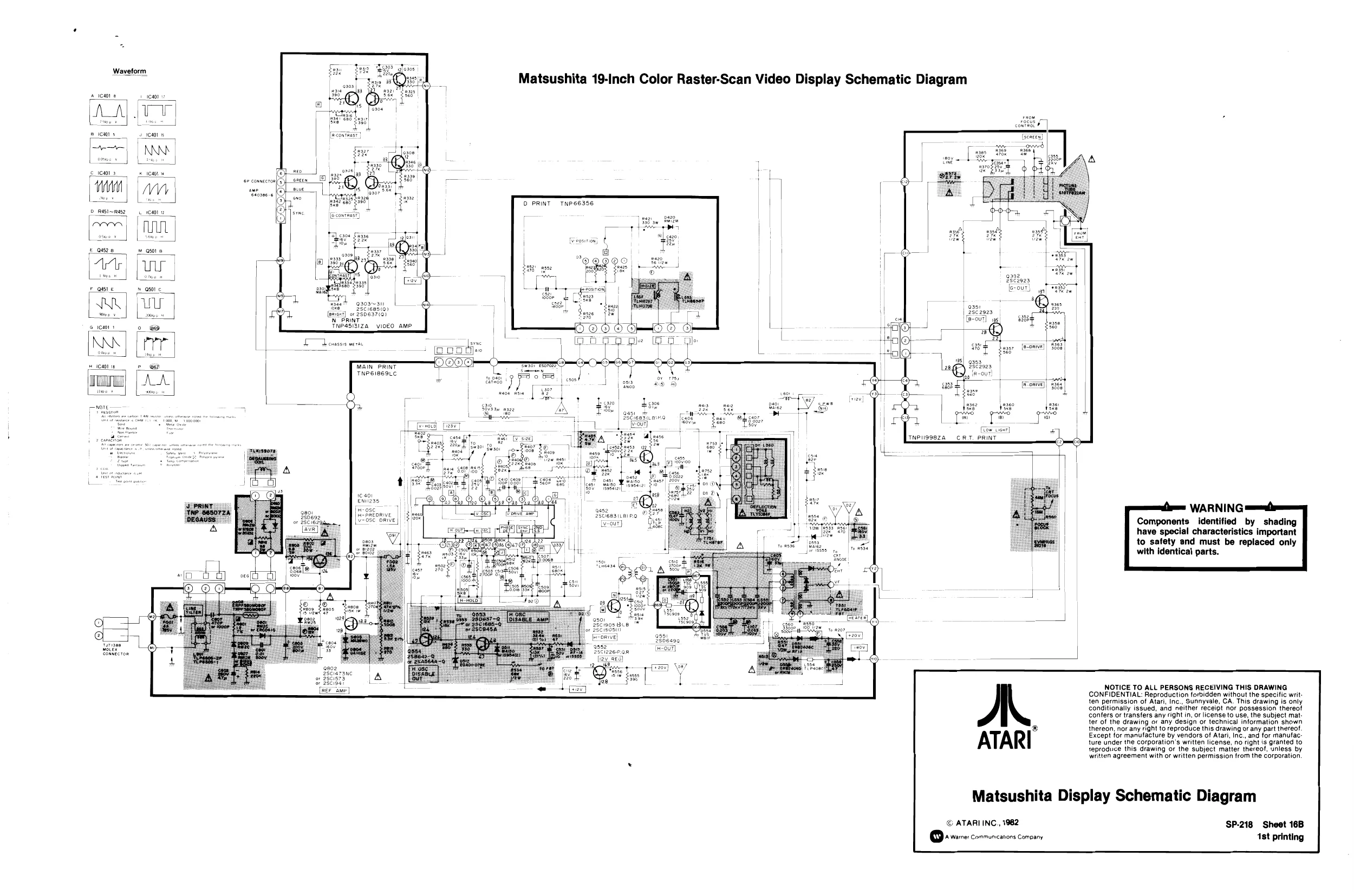
Waveform
ica w
een (vi ger ene a oRt | SEssNiza vioeo ame Te thewassis mere
TWAIN PRINT TNPSIB6SLC
- (ooo
Matsushita 19-Inch Color Raster-Scan Video Display Schematic Diagram
O PRINT TNPS6356
fooseon} t @
i 7 GOR oe Er wee Tae iron 2) | > ee Comte) 9 oo 2502923 . o Fe LA ov 175) j BR vl I J 8b B
[oot F wsag A EE alies Tweiggeza CRT PRINT fe at 9 BE FB -
28b5a90 HOUT]
NOTICE TO ALL PERSONS RECEIVING THIS DRAWING CONFIDENTIAL: Reproduction forbidden without the specific written permission of Atari, Inc., Sunnyvale, CA. This drawing is only conditionally issued, and neither receipt nor possession thereof confers or transfers any right in, or license to use, the subject matter of the drawing or any design or technical information shown thereon, nor any right to reproduce this drawing or any part thereof. Except for manufacture by vendors of Atari, Inc,, and for manufac: ture under the corporation's written license, no right is granted to seproduce this drawing or the subject matier thereof, unless by written agreement with or written permission from the corporation
Matsushita Display Schematic Diagram
© ATARI INC., 1982 SP-218 Sheet 16B